EP4411468A1 - Pixel unit of display panel, lower substrate of display panel, and display panel - Google Patents
Pixel unit of display panel, lower substrate of display panel, and display panel Download PDFInfo
- Publication number
- EP4411468A1 EP4411468A1 EP21810516.1A EP21810516A EP4411468A1 EP 4411468 A1 EP4411468 A1 EP 4411468A1 EP 21810516 A EP21810516 A EP 21810516A EP 4411468 A1 EP4411468 A1 EP 4411468A1
- Authority
- EP
- European Patent Office
- Prior art keywords
- signal line
- shielding
- common signal
- transparent
- display panel
- Prior art date
- Legal status (The legal status is an assumption and is not a legal conclusion. Google has not performed a legal analysis and makes no representation as to the accuracy of the status listed.)
- Pending
Links
Images




Classifications
-
- G—PHYSICS
- G09—EDUCATION; CRYPTOGRAPHY; DISPLAY; ADVERTISING; SEALS
- G09G—ARRANGEMENTS OR CIRCUITS FOR CONTROL OF INDICATING DEVICES USING STATIC MEANS TO PRESENT VARIABLE INFORMATION
- G09G3/00—Control arrangements or circuits, of interest only in connection with visual indicators other than cathode-ray tubes
- G09G3/20—Control arrangements or circuits, of interest only in connection with visual indicators other than cathode-ray tubes for presentation of an assembly of a number of characters, e.g. a page, by composing the assembly by combination of individual elements arranged in a matrix no fixed position being assigned to or needed to be assigned to the individual characters or partial characters
- G09G3/34—Control arrangements or circuits, of interest only in connection with visual indicators other than cathode-ray tubes for presentation of an assembly of a number of characters, e.g. a page, by composing the assembly by combination of individual elements arranged in a matrix no fixed position being assigned to or needed to be assigned to the individual characters or partial characters by control of light from an independent source
- G09G3/36—Control arrangements or circuits, of interest only in connection with visual indicators other than cathode-ray tubes for presentation of an assembly of a number of characters, e.g. a page, by composing the assembly by combination of individual elements arranged in a matrix no fixed position being assigned to or needed to be assigned to the individual characters or partial characters by control of light from an independent source using liquid crystals
- G09G3/3611—Control of matrices with row and column drivers
-
- G—PHYSICS
- G02—OPTICS
- G02F—OPTICAL DEVICES OR ARRANGEMENTS FOR THE CONTROL OF LIGHT BY MODIFICATION OF THE OPTICAL PROPERTIES OF THE MEDIA OF THE ELEMENTS INVOLVED THEREIN; NON-LINEAR OPTICS; FREQUENCY-CHANGING OF LIGHT; OPTICAL LOGIC ELEMENTS; OPTICAL ANALOGUE/DIGITAL CONVERTERS
- G02F1/00—Devices or arrangements for the control of the intensity, colour, phase, polarisation or direction of light arriving from an independent light source, e.g. switching, gating or modulating; Non-linear optics
- G02F1/01—Devices or arrangements for the control of the intensity, colour, phase, polarisation or direction of light arriving from an independent light source, e.g. switching, gating or modulating; Non-linear optics for the control of the intensity, phase, polarisation or colour
- G02F1/13—Devices or arrangements for the control of the intensity, colour, phase, polarisation or direction of light arriving from an independent light source, e.g. switching, gating or modulating; Non-linear optics for the control of the intensity, phase, polarisation or colour based on liquid crystals, e.g. single liquid crystal display cells
- G02F1/133—Constructional arrangements; Operation of liquid crystal cells; Circuit arrangements
- G02F1/136—Liquid crystal cells structurally associated with a semi-conducting layer or substrate, e.g. cells forming part of an integrated circuit
- G02F1/1362—Active matrix addressed cells
- G02F1/136218—Shield electrodes
-
- G—PHYSICS
- G02—OPTICS
- G02F—OPTICAL DEVICES OR ARRANGEMENTS FOR THE CONTROL OF LIGHT BY MODIFICATION OF THE OPTICAL PROPERTIES OF THE MEDIA OF THE ELEMENTS INVOLVED THEREIN; NON-LINEAR OPTICS; FREQUENCY-CHANGING OF LIGHT; OPTICAL LOGIC ELEMENTS; OPTICAL ANALOGUE/DIGITAL CONVERTERS
- G02F1/00—Devices or arrangements for the control of the intensity, colour, phase, polarisation or direction of light arriving from an independent light source, e.g. switching, gating or modulating; Non-linear optics
- G02F1/01—Devices or arrangements for the control of the intensity, colour, phase, polarisation or direction of light arriving from an independent light source, e.g. switching, gating or modulating; Non-linear optics for the control of the intensity, phase, polarisation or colour
- G02F1/13—Devices or arrangements for the control of the intensity, colour, phase, polarisation or direction of light arriving from an independent light source, e.g. switching, gating or modulating; Non-linear optics for the control of the intensity, phase, polarisation or colour based on liquid crystals, e.g. single liquid crystal display cells
- G02F1/133—Constructional arrangements; Operation of liquid crystal cells; Circuit arrangements
- G02F1/1333—Constructional arrangements; Manufacturing methods
-
- G—PHYSICS
- G02—OPTICS
- G02F—OPTICAL DEVICES OR ARRANGEMENTS FOR THE CONTROL OF LIGHT BY MODIFICATION OF THE OPTICAL PROPERTIES OF THE MEDIA OF THE ELEMENTS INVOLVED THEREIN; NON-LINEAR OPTICS; FREQUENCY-CHANGING OF LIGHT; OPTICAL LOGIC ELEMENTS; OPTICAL ANALOGUE/DIGITAL CONVERTERS
- G02F1/00—Devices or arrangements for the control of the intensity, colour, phase, polarisation or direction of light arriving from an independent light source, e.g. switching, gating or modulating; Non-linear optics
- G02F1/01—Devices or arrangements for the control of the intensity, colour, phase, polarisation or direction of light arriving from an independent light source, e.g. switching, gating or modulating; Non-linear optics for the control of the intensity, phase, polarisation or colour
- G02F1/13—Devices or arrangements for the control of the intensity, colour, phase, polarisation or direction of light arriving from an independent light source, e.g. switching, gating or modulating; Non-linear optics for the control of the intensity, phase, polarisation or colour based on liquid crystals, e.g. single liquid crystal display cells
- G02F1/133—Constructional arrangements; Operation of liquid crystal cells; Circuit arrangements
- G02F1/1333—Constructional arrangements; Manufacturing methods
- G02F1/1343—Electrodes
- G02F1/134309—Electrodes characterised by their geometrical arrangement
-
- G—PHYSICS
- G02—OPTICS
- G02F—OPTICAL DEVICES OR ARRANGEMENTS FOR THE CONTROL OF LIGHT BY MODIFICATION OF THE OPTICAL PROPERTIES OF THE MEDIA OF THE ELEMENTS INVOLVED THEREIN; NON-LINEAR OPTICS; FREQUENCY-CHANGING OF LIGHT; OPTICAL LOGIC ELEMENTS; OPTICAL ANALOGUE/DIGITAL CONVERTERS
- G02F1/00—Devices or arrangements for the control of the intensity, colour, phase, polarisation or direction of light arriving from an independent light source, e.g. switching, gating or modulating; Non-linear optics
- G02F1/01—Devices or arrangements for the control of the intensity, colour, phase, polarisation or direction of light arriving from an independent light source, e.g. switching, gating or modulating; Non-linear optics for the control of the intensity, phase, polarisation or colour
- G02F1/13—Devices or arrangements for the control of the intensity, colour, phase, polarisation or direction of light arriving from an independent light source, e.g. switching, gating or modulating; Non-linear optics for the control of the intensity, phase, polarisation or colour based on liquid crystals, e.g. single liquid crystal display cells
- G02F1/133—Constructional arrangements; Operation of liquid crystal cells; Circuit arrangements
- G02F1/136—Liquid crystal cells structurally associated with a semi-conducting layer or substrate, e.g. cells forming part of an integrated circuit
- G02F1/1362—Active matrix addressed cells
- G02F1/136286—Wiring, e.g. gate line, drain line
-
- G—PHYSICS
- G02—OPTICS
- G02F—OPTICAL DEVICES OR ARRANGEMENTS FOR THE CONTROL OF LIGHT BY MODIFICATION OF THE OPTICAL PROPERTIES OF THE MEDIA OF THE ELEMENTS INVOLVED THEREIN; NON-LINEAR OPTICS; FREQUENCY-CHANGING OF LIGHT; OPTICAL LOGIC ELEMENTS; OPTICAL ANALOGUE/DIGITAL CONVERTERS
- G02F1/00—Devices or arrangements for the control of the intensity, colour, phase, polarisation or direction of light arriving from an independent light source, e.g. switching, gating or modulating; Non-linear optics
- G02F1/01—Devices or arrangements for the control of the intensity, colour, phase, polarisation or direction of light arriving from an independent light source, e.g. switching, gating or modulating; Non-linear optics for the control of the intensity, phase, polarisation or colour
- G02F1/13—Devices or arrangements for the control of the intensity, colour, phase, polarisation or direction of light arriving from an independent light source, e.g. switching, gating or modulating; Non-linear optics for the control of the intensity, phase, polarisation or colour based on liquid crystals, e.g. single liquid crystal display cells
- G02F1/133—Constructional arrangements; Operation of liquid crystal cells; Circuit arrangements
- G02F1/136—Liquid crystal cells structurally associated with a semi-conducting layer or substrate, e.g. cells forming part of an integrated circuit
- G02F1/13606—Liquid crystal cells structurally associated with a semi-conducting layer or substrate, e.g. cells forming part of an integrated circuit having means for reducing parasitic capacitance
-
- G—PHYSICS
- G02—OPTICS
- G02F—OPTICAL DEVICES OR ARRANGEMENTS FOR THE CONTROL OF LIGHT BY MODIFICATION OF THE OPTICAL PROPERTIES OF THE MEDIA OF THE ELEMENTS INVOLVED THEREIN; NON-LINEAR OPTICS; FREQUENCY-CHANGING OF LIGHT; OPTICAL LOGIC ELEMENTS; OPTICAL ANALOGUE/DIGITAL CONVERTERS
- G02F2201/00—Constructional arrangements not provided for in groups G02F1/00 - G02F7/00
- G02F2201/40—Arrangements for improving the aperture ratio
-
- G—PHYSICS
- G09—EDUCATION; CRYPTOGRAPHY; DISPLAY; ADVERTISING; SEALS
- G09G—ARRANGEMENTS OR CIRCUITS FOR CONTROL OF INDICATING DEVICES USING STATIC MEANS TO PRESENT VARIABLE INFORMATION
- G09G2300/00—Aspects of the constitution of display devices
- G09G2300/04—Structural and physical details of display devices
- G09G2300/0421—Structural details of the set of electrodes
- G09G2300/0426—Layout of electrodes and connections
-
- G—PHYSICS
- G09—EDUCATION; CRYPTOGRAPHY; DISPLAY; ADVERTISING; SEALS
- G09G—ARRANGEMENTS OR CIRCUITS FOR CONTROL OF INDICATING DEVICES USING STATIC MEANS TO PRESENT VARIABLE INFORMATION
- G09G2310/00—Command of the display device
- G09G2310/02—Addressing, scanning or driving the display screen or processing steps related thereto
-
- G—PHYSICS
- G09—EDUCATION; CRYPTOGRAPHY; DISPLAY; ADVERTISING; SEALS
- G09G—ARRANGEMENTS OR CIRCUITS FOR CONTROL OF INDICATING DEVICES USING STATIC MEANS TO PRESENT VARIABLE INFORMATION
- G09G2320/00—Control of display operating conditions
- G09G2320/02—Improving the quality of display appearance
- G09G2320/0209—Crosstalk reduction, i.e. to reduce direct or indirect influences of signals directed to a certain pixel of the displayed image on other pixels of said image, inclusive of influences affecting pixels in different frames or fields or sub-images which constitute a same image, e.g. left and right images of a stereoscopic display
Definitions
- the present application relates to a field of display technologies, especially to a pixel unit of a display panel, a lower substrate of a display panel, and a display panel.
- FIG. 1 is a partial plan view of a pixel unit of a conventional liquid crystal display panel.
- the pixel unit comprises a data line DL' and a scan line SL' that perpendicularly intersect each other, and a pixel electrode element P' located at an intersection location of the data line DL' and the scan line SL'.
- the pixel electrode element P' comprises a main pixel electrode M' and a sub-pixel electrode S'.
- the pixel unit skips black matrix (Data Black Matrix Less, DBL) on the data line DL', and skips a design of using a common electrode C' as a shielding metal, but uses a wiring of the sub-pixel electrode S' as a shielding element to lower a parasitic capacitor between the main pixel electrode M' and the data line DL'.
- DBL Data Black Matrix Less
- the embodiment of the present application provides a pixel unit of a display panel, a lower substrate of a display panel, and a display panel to solve a technical issue of a excessive parasitic capacitor between a main pixel electrode of a pixel unit and a data signal line in a conventional display panel further causing serious color crosstalk and vertical crosstalk.
- an embodiment of the present application a pixel unit of a display panel, comprising:
- the transparent shielding electrode element is U-shaped, and comprises a first shielding section and two second shielding sections, the two second shielding sections extend from the common signal line into the aperture region, an end of each of the second shielding sections is connected to the common signal line, another end of each of the second shielding sections is connected to an end of the first shielding section, and an orthogonal projection of each of the second shielding sections on the plane where the common signal line is located at least partially overlaps the common signal line.
- the transparent shielding electrode element comprises two shielding bars, the two shielding bars are individual and spaced from each other, and extend from the common signal line into the aperture region, an end of each of the shielding bars is connected to the common signal line, and an orthogonal projection of each of the shielding bars on the plane where the common signal line is located at least partially overlaps the common signal line. Furthermore, the two shielding bars can be parallel.
- the transparent shielding electrode element and the common signal line are individually independent elements, and contact and are connected to each other.
- a material of the transparent shielding electrode element is indium tin oxide.
- the embodiment of the present application provides a lower substrate of the display panel, comprising a glass substrate, and a first metal layer, a second metal layer, and a first transparent conductive layer sequentially stacked on the glass substrate, wherein the lower substrate further comprises:
- the transparent shielding electrode element comprises a first shielding section and two second shielding sections extending from the first shielding section and spaced from each other, each of the second shielding sections is connected to the common signal line by contact or integral formation, and an orthogonal projection of each of the second shielding sections on the plane where the common signal line is located overlaps the common signal line for providing a shielding effect and lowering a parasitic capacitor between the pixel electrode and the data signal line.
- the transparent shielding electrode element comprises two shielding bars being individual and spaced from each other, and each of the shielding bars is connected to the common signal line by contact or integral formation, and an orthogonal projection of each of the shielding bars on the plane where the common signal line is located overlaps the common signal line. Furthermore, the two shielding bars can be parallel.
- the lower substrate further comprises a second transparent conductive layer, wherein the second transparent conductive layer is disposed between the glass substrate and the first metal layer, and the transparent shielding electrode element is formed by patterning the second transparent conductive layer.
- the transparent shielding electrode element and the common signal line are individually independent elements, and contact and are connected to each other; and a material of the transparent shielding electrode element is indium tin oxide.
- the transparent shielding electrode element comprises a first shielding section and two second shielding sections extending from the first shielding section and spaced from each other, each of the second shielding sections is connected to the common signal line by contact or integral formation, and an orthogonal projection of each of the second shielding sections on the plane where the common signal line is located overlaps the common signal line.
- the transparent shielding electrode element comprises two shielding bars being individual and spaced from each other, and each of the shielding bars is connected to the common signal line by contact or integral formation, and an orthogonal projection of each of the shielding bars on the plane where the common signal line is located overlaps the common signal line.
- the lower substrate further comprises a second transparent conductive layer, and the second transparent conductive layer is disposed between the glass substrate and the first metal layer, and the transparent shielding electrode element is formed by patterning the second transparent conductive layer.
- the embodiment of the present application provides a display panel, comprising: a lower substrate, an upper substrate disposed opposite to the lower substrate, and a liquid crystal layer disposed between the upper substrate and the lower substrate, wherein the lower substrate comprises:
- the transparent shielding electrode element comprises a first shielding section and two second shielding sections extending from the first shielding section and spaced from each other, each of the second shielding sections is connected to the common signal line by contact or integral formation, and an orthogonal projection of each of the second shielding sections on the plane where the common signal line is located overlaps the common signal line.
- the transparent shielding electrode element comprises two shielding bars being individual and spaced from each other, and each of the shielding bars is connected to the common signal line by contact or integral formation, and an orthogonal projection of each of the shielding bars on the plane where the common signal line is located overlaps the common signal line.
- the display panel further comprises a second transparent conductive layer, the second transparent conductive layer is disposed between the glass substrate and the first metal layer, and the transparent shielding electrode element is formed by patterning the second transparent conductive layer.
- the transparent shielding electrode element comprises a first shielding section and two second shielding sections extending from the first shielding section and spaced from each other, each of the second shielding sections is connected to the common signal line by contact or integral formation, and an orthogonal projection of each of the second shielding sections on the plane where the common signal line is located overlaps the common signal line;
- the transparent shielding electrode element comprises two shielding bars being individual and spaced from each other, and each of the shielding bars is connected to the common signal line by contact or integral formation, and an orthogonal projection of each of the shielding bars on the plane where the common signal line is located overlaps the common signal line; and the display panel further comprises a second transparent conductive layer, the second transparent conductive layer is disposed between the glass substrate and the first metal
- the transparent shielding electrode element and the common signal line are individually independent elements, and contact and are connected to each other.
- a material of the transparent shielding electrode element is indium tin oxide.
- the present application at least comprises advantages as follows:
- the pixel unit of the display panel, the lower substrate of the display panel, and the display panel provided by the present application by disposing a transparent shielding electrode element connected to a common signal line and extending into the aperture region and making an orthogonal projection of the transparent shielding electrode element on a plane where the common signal line is located at least partially overlap the common signal line, extends a shielding effect provided by the common signal line such that a parasitic capacitor between the pixel electrode and the data line is lowered to solve the technical issue of a excessive parasitic capacitor between a main pixel electrode portion of a pixel unit and a data signal line in a conventional display panel further causing serious color crosstalk and vertical crosstalk.
- the transparent shielding electrode element and the pixel electrode of the present application are transparent conductive electrodes, therefore the transparent shielding electrode element extending into the aperture region would not reduce an aperture rate and a transmittance of the pixel unit to prevent reduction of the aperture rate and the transmittance of a shielding metal of the conventional pixel unit located in the aperture region.
- the embodiment of the present application provides a pixel unit of a display panel, a lower substrate of a display panel, and a display panel to solve a technical issue of a excessive parasitic capacitor between a main pixel electrode of a pixel unit and a data signal line in a conventional display panel further causing serious color crosstalk and vertical crosstalk.
- the pixel unit 3 of the display panel provided by the embodiment of the present application comprises: a scan signal line SL, a data signal line DL, a common signal line CL, a pixel electrode P, and a transparent shielding electrode element 20.
- a gate electrode G is formed on the scan signal line SL.
- the data signal line DL perpendicularly intersects the scan signal line SL.
- An aperture region OA is formed in an intersection location between the scan signal line SL and the data signal line DL, as shown in FIG. 3b .
- the common signal line CL is disposed to be parallel to the scan signal line SL, and a common electrode C is formed on the common signal line CL.
- the pixel electrode P is disposed in the aperture region OA and can comprise a main pixel electrode portion M and a sub-pixel electrode portion S.
- the transparent shielding electrode element 20 is connected to the common signal line CL and extends from the common signal line CL into the aperture region OA, and an orthogonal projection of the transparent shielding electrode element 20 on a plane where the common signal line CL is located at least partially overlaps the common signal line CL.
- a part of the common signal line CL covers a part of the transparent shielding electrode element 20, or a part of the transparent shielding electrode element 20 covers a part of the common signal line CL.
- the transparent shielding electrode element 20 serves as an electrode for extending a shielding effect of the common signal line CL to further lower the parasitic capacitor between the main pixel electrode portion M and the data signal line DL to further prevent the issues of color crosstalk and vertical crosstalk.
- a material of the transparent shielding electrode element 20 can be indium tin oxide (ITO).
- the transparent shielding electrode element 20 is U-shaped, comprises 1 first shielding section 21 and two second shielding sections 22.
- the two second shielding sections 22 extend from the common electrode C into the aperture region OA.
- An end of each of the second shielding sections 22 is connected to the common signal line CL, and another end of each of the second shielding sections 22 is connected to an end of the first shielding section 21.
- the two second shielding sections 22 are located near the data signal line DL of the pixel unit and another data signal line DL of an adjacent pixel unit further included by the display panel and the two second shielding sections 22 can located on two sides of main pixel electrode portion M of the pixel electrode P to further lower the parasitic capacitor between the main pixel electrode portion M and the data signal line DL.
- the transparent shielding electrode element 20a comprises two shielding bars 23.
- the two shielding bars 23 are individual and spaced from each other, extend from the common signal line CL into the aperture region OA, and an end of each of the shielding bars 23 is connected to the common signal line CL.
- the two shielding bars 23 are located near the data signal line DL of the pixel unit and another data signal line DL of an adjacent pixel unit further included by the display panel, and the two shielding bars 23 can be located on two sides of main pixel electrode portion M of the pixel electrode P to further lower the parasitic capacitor between the main pixel electrode portion M and the data signal line DL.
- the transparent shielding electrode element 20 and the common signal line CL are located in different material layers, are elements being individual and separated from each other, and contact and are connected to each other.
- both the transparent shielding electrode element 20 and the common signal line CL are disposed on a surface of the glass substrate 10, and a part of the common electrode C covers a part of the transparent shielding electrode element 20, or a part of the transparent shielding electrode element 20 covers a part of the common electrode C.
- the lower substrate of the display panel 1 provided by the embodiment of the present application, comprises a glass substrate 10, and a first metal layer M1, a second metal layer M2, and a first transparent conductive layer 30 sequentially stacked on the glass substrate 10, wherein the lower substrate 1 further comprises : a scan signal line SL, a data signal line DL, a common signal line CL, pixel electrode P, and a transparent shielding electrode element 20.
- the scan signal line SL is formed by patterning the first metal layer M1, and a gate electrode G is formed on the scan signal line SL.
- the data signal line DL is formed by patterning the second metal layer M2, perpendicularly intersects the scan signal line SL.
- an aperture region OA is formed in an intersection location between the scan signal line SL and the data signal line DL.
- the common signal line CL is disposed in a same layer with the scan signal line SL and is parallel to the scan signal line SL.
- a common electrode C is formed on the common signal line CL.
- the pixel electrode P is formed by patterning the first transparent conductive layer 30, is disposed in the aperture region OA, and can comprise a main pixel electrode portion M and a sub-pixel electrode portion S.
- the transparent shielding electrode element 20 is connected to the common signal line CL, extends from the common signal line CL into the aperture region, and an orthogonal projection of the transparent shielding electrode element 20 on the plane where the common signal line CL is located at least partially overlap the common signal line CL.
- the transparent shielding electrode element 20 serves as a shielding electrode to shield the common signal line CL to further lower a parasitic capacitor between the main pixel electrode portion M and the data signal line DL, and further prevent the issues of color crosstalk and vertical crosstalk.
- a material of the transparent shielding electrode element 20 can be indium tin oxide (ITO).
- the transparent shielding electrode element 20 is U-shaped and comprises a first shielding section 21 and two second shielding sections 22.
- the two second shielding sections 22 extend from the common signal line CL into the aperture region.
- An end of each of the second shielding sections 22 is connected to the common signal line CL, and another end of each of the second shielding sections 22 is connected to an end of the first shielding section 21.
- An orthogonal projection of each of the second shielding sections 22 on the plane where the common signal line CL is located at least partially overlap the common signal line CL.
- the two second shielding sections 22 are located near the data signal line DL of the pixel unit and another data signal line DL of an adjacent the pixel unit further included by the display panel, and the two second shielding sections 22 can be located on two sides of the main pixel electrode portion M of the pixel electrode P respectively to further lower a parasitic capacitor between the main pixel electrode portion M and the data signal line DL.
- the lower substrate of the display panel 1 provided by the embodiment of the present application further comprises an insulation layer GI, semiconductor layer (not shown), a first passivation layer PV1, a color photoresist layer CF, and a second passivation layer PV2.
- the glass substrate 10, the first metal layer M1, the insulation layer GI, the semiconductor layer, the second metal layer M2, the first passivation layer PV1, the color photoresist layer CF, the second passivation layer PV2, and the first transparent conductive layer 30 are sequentially stacked on one another to form the lower substrate 1.
- the transparent shielding electrode element 20 comprises two shielding bars 23.
- the two shielding bars 23 are individual and spaced from each other, and extend from the common signal line CL into the aperture region.
- An end of each of the shielding bars 23 is connected to the common signal line CL, and an orthogonal projection of each of the shielding bars 23 on the plane where the common signal line CL is located at least partially overlap the common signal line CL.
- the two shielding bars 23 are located near the data signal line DL of the pixel unit and another data signal line DL of an adjacent pixel unit further included by the display panel, and the two shielding bars 23 can be located two sides of the main pixel electrode portion M of the pixel electrode P respectively to further lower the parasitic capacitor between the main pixel electrode portion M and the data signal line DL.
- the transparent shielding electrode element 20 is formed by patterning the second transparent conductive layer.
- the second transparent conductive layer is disposed between the glass substrate 10 and the first metal layer M1.
- the transparent shielding electrode element 20 is formed by patterning the second transparent conductive layer with a lithography process.
- the display panel provided by the embodiment of the present application comprises: the lower substrate 1 of the above embodiment, an upper substrate 2 disposed opposite to the lower substrate 1, and a liquid crystal layer LC disposed between the upper substrate 2 and the lower substrate 1.
- upper substrate 2 further comprises a black matrix BM to define the aperture region OA.
- the upper substrate 2 further comprises an upper substrate common electrode CC and a top cover CG, as shown in FIG. 2 .
- the following comparison table is for comparison between a parasitic capacitor of the above pixel unit before increasing the transparent shielding electrode element 20 and after increasing the transparent shielding electrode element 20. It can be understood from the comparison table that after the U-shaped transparent electrode is increased, the parasitic capacitor of the main pixel electrode portion M can be decreased to 12% of an original value, and the parasitic capacitor/total capacitor is reduced from 1.24% to 0.15%, which indicates that the transparent shielding electrode element 20 has a parasitic capacitor reduction effect. When an area of the transparent shielding electrode element 20 is sufficiently increased, the parasitic capacitor/total capacitor would be smaller.
- the pixel unit of the display panel, the lower substrate 1 of the display panel, and the display panel provided by the present application by disposing a transparent shielding electrode element 20 connected to a common electrode C and extending into the aperture region and making an orthogonal projection of the transparent shielding electrode element 20 on a plane where the common signal line CL is located at least partially overlap the common signal line CL, extends a shielding effect provided by the common signal line CL such that a parasitic capacitor between the pixel electrode and the data line is lowered to solve the technical issue of a excessive parasitic capacitor between a main pixel electrode portion M of a pixel unit and a data signal line in a conventional display panel further causing serious color crosstalk and vertical crosstalk.
- the transparent shielding electrode element 20 and the pixel electrode P of the present application are transparent conductive electrodes, therefore the transparent shielding electrode element 20 extending into the aperture region would not reduce an aperture rate and a transmittance of the pixel unit to prevent reduction of the aperture rate and the transmittance of a shielding metal of the conventional pixel unit located in the aperture region.
Landscapes
- Physics & Mathematics (AREA)
- Nonlinear Science (AREA)
- Crystallography & Structural Chemistry (AREA)
- General Physics & Mathematics (AREA)
- Chemical & Material Sciences (AREA)
- Mathematical Physics (AREA)
- Optics & Photonics (AREA)
- Engineering & Computer Science (AREA)
- Microelectronics & Electronic Packaging (AREA)
- Geometry (AREA)
- Computer Hardware Design (AREA)
- Theoretical Computer Science (AREA)
- Devices For Indicating Variable Information By Combining Individual Elements (AREA)
- Liquid Crystal (AREA)
Abstract
Description
- The present application relates to a field of display technologies, especially to a pixel unit of a display panel, a lower substrate of a display panel, and a display panel.
- With development of liquid crystal display panel technologies, a transmittance of a pixel on display panel almost reaches the limit. Various pixel designs of conventional display panels all aim at simplification of wiring to increase an aperture region area to further raise an aperture rate and improve the transmittance.
- With reference to
FIG. 1, FIG. 1 is a partial plan view of a pixel unit of a conventional liquid crystal display panel. The pixel unit comprises a data line DL' and a scan line SL' that perpendicularly intersect each other, and a pixel electrode element P' located at an intersection location of the data line DL' and the scan line SL'. The pixel electrode element P' comprises a main pixel electrode M' and a sub-pixel electrode S'. To increase an aperture rate of the display panel, the pixel unit skips black matrix (Data Black Matrix Less, DBL) on the data line DL', and skips a design of using a common electrode C' as a shielding metal, but uses a wiring of the sub-pixel electrode S' as a shielding element to lower a parasitic capacitor between the main pixel electrode M' and the data line DL'. However, such pixel unit design has an issue that the sub-pixel electrode S' in most of the time is floating without potential control such that it's shielding function is very limited and results in an excessively large parasitic capacitor between the main pixel electrode M' and the data line DL', which results in serious issues of color crosstalk and vertical crosstalk. - The embodiment of the present application provides a pixel unit of a display panel, a lower substrate of a display panel, and a display panel to solve a technical issue of a excessive parasitic capacitor between a main pixel electrode of a pixel unit and a data signal line in a conventional display panel further causing serious color crosstalk and vertical crosstalk.
- In an aspect, an embodiment of the present application a pixel unit of a display panel, comprising:
- a scan signal line;
- a data signal line perpendicularly intersecting the scan signal line, wherein an aperture region is formed in an intersection location between the scan signal line and the data signal line;
- a common signal line disposed to be parallel to the scan signal line, wherein a common electrode is formed on the common signal line;
- a pixel electrode disposed in the aperture region; and
- a transparent shielding electrode element connected to the common signal line and extending from the common signal line into the aperture region, wherein an orthogonal projection of the transparent shielding electrode element on a plane where the common signal line is located at least partially overlap the common signal line.
- In some embodiments of the present application, the transparent shielding electrode element is U-shaped, and comprises a first shielding section and two second shielding sections, the two second shielding sections extend from the common signal line into the aperture region, an end of each of the second shielding sections is connected to the common signal line, another end of each of the second shielding sections is connected to an end of the first shielding section, and an orthogonal projection of each of the second shielding sections on the plane where the common signal line is located at least partially overlaps the common signal line.
- In some embodiments of the present application, the transparent shielding electrode element comprises two shielding bars, the two shielding bars are individual and spaced from each other, and extend from the common signal line into the aperture region, an end of each of the shielding bars is connected to the common signal line, and an orthogonal projection of each of the shielding bars on the plane where the common signal line is located at least partially overlaps the common signal line. Furthermore, the two shielding bars can be parallel.
- In some embodiments of the present application, the transparent shielding electrode element and the common signal line are individually independent elements, and contact and are connected to each other.
- In some embodiments of the present application, a material of the transparent shielding electrode element is indium tin oxide.
- In another aspect, the embodiment of the present application provides a lower substrate of the display panel, comprising a glass substrate, and a first metal layer, a second metal layer, and a first transparent conductive layer sequentially stacked on the glass substrate, wherein the lower substrate further comprises:
- a scan signal line formed by patterning the first metal layer;
- a data signal line formed by patterning the second metal layer, perpendicularly intersecting the scan signal line, wherein an aperture region is formed in an intersection location between the scan signal line and the data signal line;
- a common signal line disposed on a same layer with the scan signal line and parallel to the scan signal line, wherein a common electrode is formed on the common signal line;
- a pixel electrode formed by patterning the first transparent conductive layer, and disposed in the aperture region; and
- a transparent shielding electrode element connected to the common signal line, extending from the common signal line into the aperture region, and an orthogonal projection of the transparent shielding electrode element on a plane where the common signal line is located at least partially overlaps the common signal line for providing a shielding effect and lower a parasitic capacitor between the pixel electrode and the data signal line.
- In some embodiments of the present application, the transparent shielding electrode element comprises a first shielding section and two second shielding sections extending from the first shielding section and spaced from each other, each of the second shielding sections is connected to the common signal line by contact or integral formation, and an orthogonal projection of each of the second shielding sections on the plane where the common signal line is located overlaps the common signal line for providing a shielding effect and lowering a parasitic capacitor between the pixel electrode and the data signal line.
- In some embodiments of the present application, the transparent shielding electrode element comprises two shielding bars being individual and spaced from each other, and each of the shielding bars is connected to the common signal line by contact or integral formation, and an orthogonal projection of each of the shielding bars on the plane where the common signal line is located overlaps the common signal line. Furthermore, the two shielding bars can be parallel.
- In some embodiments of the present application, the lower substrate further comprises a second transparent conductive layer, wherein the second transparent conductive layer is disposed between the glass substrate and the first metal layer, and the transparent shielding electrode element is formed by patterning the second transparent conductive layer.
- In some embodiments of the present application, the transparent shielding electrode element and the common signal line are individually independent elements, and contact and are connected to each other; and
a material of the transparent shielding electrode element is indium tin oxide. - In some embodiments of the present application, the transparent shielding electrode element comprises a first shielding section and two second shielding sections extending from the first shielding section and spaced from each other, each of the second shielding sections is connected to the common signal line by contact or integral formation, and an orthogonal projection of each of the second shielding sections on the plane where the common signal line is located overlaps the common signal line.
- In some embodiments of the present application, the transparent shielding electrode element comprises two shielding bars being individual and spaced from each other, and each of the shielding bars is connected to the common signal line by contact or integral formation, and an orthogonal projection of each of the shielding bars on the plane where the common signal line is located overlaps the common signal line.
- In some embodiments of the present application, the lower substrate, further comprises a second transparent conductive layer, and the second transparent conductive layer is disposed between the glass substrate and the first metal layer, and the transparent shielding electrode element is formed by patterning the second transparent conductive layer.
- In another aspect, the embodiment of the present application provides a display panel, comprising: a lower substrate, an upper substrate disposed opposite to the lower substrate, and a liquid crystal layer disposed between the upper substrate and the lower substrate, wherein the lower substrate comprises:
- a glass substrate, and a first metal layer, a second metal layer, and a first transparent conductive layer sequentially stacked on the glass substrate,;
- a scan signal line formed by patterning the first metal layer;
- a data signal line formed by patterning the second metal layer, perpendicularly intersecting the scan signal line, wherein an aperture region is formed in an intersection location between the scan signal line and the data signal line;
- a common signal line disposed on a same layer with the scan signal line and parallel to the scan signal line, wherein a common electrode is formed on the common signal line;
- a pixel electrode formed by patterning the first transparent conductive layer, and disposed in the aperture region; and
- a transparent shielding electrode element connected to the common signal line, extending from the common signal line into the aperture region, and an orthogonal projection of the transparent shielding electrode element on a plane where the common signal line is located at least partially overlaps the common signal line.
- In some embodiments of the present application, the transparent shielding electrode element comprises a first shielding section and two second shielding sections extending from the first shielding section and spaced from each other, each of the second shielding sections is connected to the common signal line by contact or integral formation, and an orthogonal projection of each of the second shielding sections on the plane where the common signal line is located overlaps the common signal line.
- In some embodiments of the present application, the transparent shielding electrode element comprises two shielding bars being individual and spaced from each other, and each of the shielding bars is connected to the common signal line by contact or integral formation, and an orthogonal projection of each of the shielding bars on the plane where the common signal line is located overlaps the common signal line.
- In some embodiments of the present application, the display panel further comprises a second transparent conductive layer, the second transparent conductive layer is disposed between the glass substrate and the first metal layer, and the transparent shielding electrode element is formed by patterning the second transparent conductive layer. In some embodiments of the present application, the transparent shielding electrode element comprises a first shielding section and two second shielding sections extending from the first shielding section and spaced from each other, each of the second shielding sections is connected to the common signal line by contact or integral formation, and an orthogonal projection of each of the second shielding sections on the plane where the common signal line is located overlaps the common signal line; the transparent shielding electrode element comprises two shielding bars being individual and spaced from each other, and each of the shielding bars is connected to the common signal line by contact or integral formation, and an orthogonal projection of each of the shielding bars on the plane where the common signal line is located overlaps the common signal line; and the display panel further comprises a second transparent conductive layer, the second transparent conductive layer is disposed between the glass substrate and the first metal layer, and the transparent shielding electrode element is formed by patterning the second transparent conductive layer.
- In some embodiments of the present application, the transparent shielding electrode element and the common signal line are individually independent elements, and contact and are connected to each other.
- In some embodiments of the present application, a material of the transparent shielding electrode element is indium tin oxide.
- The present application at least comprises advantages as follows:
The pixel unit of the display panel, the lower substrate of the display panel, and the display panel provided by the present application, by disposing a transparent shielding electrode element connected to a common signal line and extending into the aperture region and making an orthogonal projection of the transparent shielding electrode element on a plane where the common signal line is located at least partially overlap the common signal line, extends a shielding effect provided by the common signal line such that a parasitic capacitor between the pixel electrode and the data line is lowered to solve the technical issue of a excessive parasitic capacitor between a main pixel electrode portion of a pixel unit and a data signal line in a conventional display panel further causing serious color crosstalk and vertical crosstalk. Furthermore, because the transparent shielding electrode element and the pixel electrode of the present application are transparent conductive electrodes, therefore the transparent shielding electrode element extending into the aperture region would not reduce an aperture rate and a transmittance of the pixel unit to prevent reduction of the aperture rate and the transmittance of a shielding metal of the conventional pixel unit located in the aperture region. - To more clearly elaborate on the technical solutions of embodiments of the present invention or prior art, appended figures necessary for describing the embodiments of the present invention or prior art will be briefly introduced as follows. Apparently, the following appended figures are merely some embodiments of the present invention. A person of ordinary skill in the art may acquire other figures according to the appended figures without any creative effort.
-
FIG. 1 is a schematic plan view of a pixel unit of a conventional display panel; -
FIG. 2 is a schematic exploded perspective view of a display panel provided by an embodiment of the present application; -
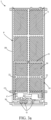
FIG. 3a is a schematic plan view of the pixel unit of the display panel provided by the embodiment of the present application; -
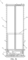
FIG. 3b is a schematic plan view of the pixel unit of the display panel provided by the embodiment of the present application, wherein pixel electrode is omitted and an aperture region is marked out; -
FIG. 4 is a schematic plan view of a common signal line in a first metal layer of the pixel unit of the display panel provided by the embodiment of the present application partially overlapping a transparent shielding electrode element; -
FIG. 5 is a schematic plan view of the pixel unit of the display panel provided by another embodiment of the present application; and -
FIG. 6 is a schematic plan view of the common signal line of the first metal layer in the pixel unit of the display panel provided by another embodiment of the present application partially overlapping the transparent shielding electrode element. - The technical solution in the embodiment of the present application will be clearly and completely described below with reference to the accompanying drawings in the embodiments of the present application. Apparently, the described embodiments are merely some embodiments of the present application instead of all embodiments. According to the embodiments in the present application, all other embodiments obtained by those skilled in the art without making any creative effort shall fall within the protection scope of the present application.
- In addition, it should be understood that the specific embodiments described here are only used to illustrate and explain the present application, and are not used to limit the present application. In the present application, the used orientation terminologies such as "upper" and "lower", when are not specified to the contrary explanation, usually refer to the upper and lower states of the device in actual use or working conditions, specifically according to the direction of the figures in the drawings. Furthermore, "inner" and "outer" refer to the outline of the device.
- The embodiment of the present application provides a pixel unit of a display panel, a lower substrate of a display panel, and a display panel to solve a technical issue of a excessive parasitic capacitor between a main pixel electrode of a pixel unit and a data signal line in a conventional display panel further causing serious color crosstalk and vertical crosstalk.
- With reference to
FIGs. 2 ,3a and3b , thepixel unit 3 of the display panel provided by the embodiment of the present application comprises: a scan signal line SL, a data signal line DL, a common signal line CL, a pixel electrode P, and a transparentshielding electrode element 20. - A gate electrode G is formed on the scan signal line SL.
- The data signal line DL perpendicularly intersects the scan signal line SL. An aperture region OA is formed in an intersection location between the scan signal line SL and the data signal line DL, as shown in
FIG. 3b . - The common signal line CL is disposed to be parallel to the scan signal line SL, and a common electrode C is formed on the common signal line CL.
- The pixel electrode P is disposed in the aperture region OA and can comprise a main pixel electrode portion M and a sub-pixel electrode portion S.
- The transparent
shielding electrode element 20 is connected to the common signal line CL and extends from the common signal line CL into the aperture region OA, and an orthogonal projection of the transparentshielding electrode element 20 on a plane where the common signal line CL is located at least partially overlaps the common signal line CL. In particular, a part of the common signal line CL covers a part of the transparentshielding electrode element 20, or a part of the transparentshielding electrode element 20 covers a part of the common signal line CL. - In particular, the transparent
shielding electrode element 20 serves as an electrode for extending a shielding effect of the common signal line CL to further lower the parasitic capacitor between the main pixel electrode portion M and the data signal line DL to further prevent the issues of color crosstalk and vertical crosstalk. In a preferred embodiment of the present application, a material of the transparentshielding electrode element 20 can be indium tin oxide (ITO). - With reference to
FIGs. 3a ,3b , and4 , in an embodiment of the present application, the transparentshielding electrode element 20 is U-shaped, comprises 1first shielding section 21 and twosecond shielding sections 22. The twosecond shielding sections 22 extend from the common electrode C into the aperture region OA. An end of each of thesecond shielding sections 22 is connected to the common signal line CL, and another end of each of thesecond shielding sections 22 is connected to an end of thefirst shielding section 21. An orthogonal projection of each of thesecond shielding sections 22 on the plane where the common signal line CL is located at least partially overlap the common signal line CL. Furthermore, the twosecond shielding sections 22 are located near the data signal line DL of the pixel unit and another data signal line DL of an adjacent pixel unit further included by the display panel and the twosecond shielding sections 22 can located on two sides of main pixel electrode portion M of the pixel electrode P to further lower the parasitic capacitor between the main pixel electrode portion M and the data signal line DL. - With reference to
FIGs. 5 and6 , in another embodiment of the present application, the transparentshielding electrode element 20a comprises two shielding bars 23. The two shieldingbars 23 are individual and spaced from each other, extend from the common signal line CL into the aperture region OA, and an end of each of the shielding bars 23 is connected to the common signal line CL. An orthogonal projection of each of the shielding bars 23 on the plane where the common signal line CL is located at least partially overlap the common signal line CL. Furthermore, the two shieldingbars 23 are located near the data signal line DL of the pixel unit and another data signal line DL of an adjacent pixel unit further included by the display panel, and the two shieldingbars 23 can be located on two sides of main pixel electrode portion M of the pixel electrode P to further lower the parasitic capacitor between the main pixel electrode portion M and the data signal line DL. - In some embodiments of the present application, the transparent
shielding electrode element 20 and the common signal line CL are located in different material layers, are elements being individual and separated from each other, and contact and are connected to each other. Alternatively, in some embodiments of the present application, both the transparentshielding electrode element 20 and the common signal line CL are disposed on a surface of theglass substrate 10, and a part of the common electrode C covers a part of the transparentshielding electrode element 20, or a part of the transparentshielding electrode element 20 covers a part of the common electrode C. - With reference to
FIGs. 2 ,3a , and3b , the lower substrate of the display panel 1 provided by the embodiment of the present application, comprises aglass substrate 10, and a first metal layer M1, a second metal layer M2, and a first transparentconductive layer 30 sequentially stacked on theglass substrate 10, wherein the lower substrate 1 further comprises : a scan signal line SL, a data signal line DL, a common signal line CL, pixel electrode P, and a transparentshielding electrode element 20. - The scan signal line SL is formed by patterning the first metal layer M1, and a gate electrode G is formed on the scan signal line SL.
- The data signal line DL is formed by patterning the second metal layer M2, perpendicularly intersects the scan signal line SL. an aperture region OA is formed in an intersection location between the scan signal line SL and the data signal line DL.
- The common signal line CL is disposed in a same layer with the scan signal line SL and is parallel to the scan signal line SL. A common electrode C is formed on the common signal line CL.
- The pixel electrode P is formed by patterning the first transparent
conductive layer 30, is disposed in the aperture region OA, and can comprise a main pixel electrode portion M and a sub-pixel electrode portion S. - The transparent
shielding electrode element 20 is connected to the common signal line CL, extends from the common signal line CL into the aperture region, and an orthogonal projection of the transparentshielding electrode element 20 on the plane where the common signal line CL is located at least partially overlap the common signal line CL. - In particular, the transparent
shielding electrode element 20 serves as a shielding electrode to shield the common signal line CL to further lower a parasitic capacitor between the main pixel electrode portion M and the data signal line DL, and further prevent the issues of color crosstalk and vertical crosstalk. In a preferred embodiment of the present application, a material of the transparentshielding electrode element 20 can be indium tin oxide (ITO). - With reference to
FIGs. 3a ,3b , and4 , in an embodiment of the present application, the transparentshielding electrode element 20 is U-shaped and comprises afirst shielding section 21 and twosecond shielding sections 22. The twosecond shielding sections 22 extend from the common signal line CL into the aperture region. An end of each of thesecond shielding sections 22 is connected to the common signal line CL, and another end of each of thesecond shielding sections 22 is connected to an end of thefirst shielding section 21. An orthogonal projection of each of thesecond shielding sections 22 on the plane where the common signal line CL is located at least partially overlap the common signal line CL. Furthermore, the twosecond shielding sections 22 are located near the data signal line DL of the pixel unit and another data signal line DL of an adjacent the pixel unit further included by the display panel, and the twosecond shielding sections 22 can be located on two sides of the main pixel electrode portion M of the pixel electrode P respectively to further lower a parasitic capacitor between the main pixel electrode portion M and the data signal line DL. - In particular, the lower substrate of the display panel 1 provided by the embodiment of the present application further comprises an insulation layer GI, semiconductor layer (not shown), a first passivation layer PV1, a color photoresist layer CF, and a second passivation layer PV2. The
glass substrate 10, the first metal layer M1, the insulation layer GI, the semiconductor layer, the second metal layer M2, the first passivation layer PV1, the color photoresist layer CF, the second passivation layer PV2, and the first transparentconductive layer 30 are sequentially stacked on one another to form the lower substrate 1. - With reference to
FIGs. 5 and6 , in another embodiment of the present application, the transparentshielding electrode element 20 comprises two shielding bars 23. The two shieldingbars 23 are individual and spaced from each other, and extend from the common signal line CL into the aperture region. An end of each of the shielding bars 23 is connected to the common signal line CL, and an orthogonal projection of each of the shielding bars 23 on the plane where the common signal line CL is located at least partially overlap the common signal line CL. Furthermore, the two shieldingbars 23 are located near the data signal line DL of the pixel unit and another data signal line DL of an adjacent pixel unit further included by the display panel, and the two shieldingbars 23 can be located two sides of the main pixel electrode portion M of the pixel electrode P respectively to further lower the parasitic capacitor between the main pixel electrode portion M and the data signal line DL. - In some embodiments of the present application, the transparent
shielding electrode element 20 is formed by patterning the second transparent conductive layer. In particular, the second transparent conductive layer is disposed between theglass substrate 10 and the first metal layer M1. The transparentshielding electrode element 20 is formed by patterning the second transparent conductive layer with a lithography process. - In another aspect, the display panel provided by the embodiment of the present application comprises: the lower substrate 1 of the above embodiment, an upper substrate 2 disposed opposite to the lower substrate 1, and a liquid crystal layer LC disposed between the upper substrate 2 and the lower substrate 1. In particular, upper substrate 2 further comprises a black matrix BM to define the aperture region OA. Furthermore, the upper substrate 2 further comprises an upper substrate common electrode CC and a top cover CG, as shown in
FIG. 2 . - The following comparison table is for comparison between a parasitic capacitor of the above pixel unit before increasing the transparent
shielding electrode element 20 and after increasing the transparentshielding electrode element 20. It can be understood from the comparison table that after the U-shaped transparent electrode is increased, the parasitic capacitor of the main pixel electrode portion M can be decreased to 12% of an original value, and the parasitic capacitor/total capacitor is reduced from 1.24% to 0.15%, which indicates that the transparentshielding electrode element 20 has a parasitic capacitor reduction effect. When an area of the transparentshielding electrode element 20 is sufficiently increased, the parasitic capacitor/total capacitor would be smaller.Main pixel electrode portion M Before increase of the transparent shielding electrode element 20After increase of the U-shaped transparent shielding electrode element 20After increase of 11-shaped transparent shielding electrode element 20Parasitic capacitor [fF] 4.070 0.486 0.561 Total capacitor [fF] 327.560 333.259 331.566 Parasitic capacitor/Total capacitor 1.24% 0.15% 0.17% - The present application at least comprises advantages as follows:
- The pixel unit of the display panel, the lower substrate 1 of the display panel, and the display panel provided by the present application, by disposing a transparent
shielding electrode element 20 connected to a common electrode C and extending into the aperture region and making an orthogonal projection of the transparentshielding electrode element 20 on a plane where the common signal line CL is located at least partially overlap the common signal line CL, extends a shielding effect provided by the common signal line CL such that a parasitic capacitor between the pixel electrode and the data line is lowered to solve the technical issue of a excessive parasitic capacitor between a main pixel electrode portion M of a pixel unit and a data signal line in a conventional display panel further causing serious color crosstalk and vertical crosstalk. Furthermore, because the transparentshielding electrode element 20 and the pixel electrode P of the present application are transparent conductive electrodes, therefore the transparentshielding electrode element 20 extending into the aperture region would not reduce an aperture rate and a transmittance of the pixel unit to prevent reduction of the aperture rate and the transmittance of a shielding metal of the conventional pixel unit located in the aperture region. - In the specification, the specific examples are used to explain the principle and embodiment of the present application. The above description of the embodiments is only used to help understand the method of the present application and its spiritual idea. Meanwhile, for those skilled in the art, according to the present the idea of invention, changes will be made in specific embodiment and application. In summary, the contents of this specification should not be construed as limiting the present application.
Claims (20)
- A pixel unit of a display panel, comprising:a scan signal line;a data signal line perpendicularly intersecting the scan signal line, wherein an aperture region is formed in an intersection location between the scan signal line and the data signal line;a common signal line disposed to be parallel to the scan signal line, wherein a common electrode is formed on the common signal line;a pixel electrode disposed in the aperture region; anda transparent shielding electrode element connected to the common signal line and extending from the common signal line into the aperture region, wherein an orthogonal projection of the transparent shielding electrode element on a plane where the common signal line is located at least partially overlap the common signal line.
- The pixel unit of the display panel according to claim 1, wherein the transparent shielding electrode element is U-shaped, and comprises a first shielding section and two second shielding sections, the two second shielding sections extend from the common signal line into the aperture region, an end of each of the second shielding sections is connected to the common signal line, another end of each of the second shielding sections is connected to an end of the first shielding section, and an orthogonal projection of each of the second shielding sections on the plane where the common signal line is located at least partially overlaps the common signal line.
- The pixel unit of the display panel according to claim 1, wherein the transparent shielding electrode element comprises two shielding bars, the two shielding bars are individual and spaced from each other, and extend from the common signal line into the aperture region, an end of each of the shielding bars is connected to the common signal line, and an orthogonal projection of each of the shielding bars on the plane where the common signal line is located at least partially overlaps the common signal line.
- The pixel unit of the display panel according to claim 1, wherein the transparent shielding electrode element and the common signal line are individually independent elements, and contact and are connected to each other.
- The pixel unit of the display panel according to claim 1, wherein a material of the transparent shielding electrode element is indium tin oxide.
- A lower substrate of a display panel, comprising a glass substrate, and a first metal layer, a second metal layer, and a first transparent conductive layer sequentially stacked on the glass substrate, wherein the lower substrate further comprises:a scan signal line formed by patterning the first metal layer;a data signal line formed by patterning the second metal layer, perpendicularly intersecting the scan signal line, wherein an aperture region is formed in an intersection location between the scan signal line and the data signal line;a common signal line disposed on a same layer with the scan signal line and parallel to the scan signal line, wherein a common electrode is formed on the common signal line;a pixel electrode formed by patterning the first transparent conductive layer, and disposed in the aperture region; anda transparent shielding electrode element connected to the common signal line, extending from the common signal line into the aperture region, and an orthogonal projection of the transparent shielding electrode element on a plane where the common signal line is located at least partially overlaps the common signal line for providing a shielding effect and lower a parasitic capacitor between the pixel electrode and the data signal line.
- The lower substrate of the display panel according to claim 6, wherein the transparent shielding electrode element comprises a first shielding section and two second shielding sections extending from the first shielding section and spaced from each other, each of the second shielding sections is connected to the common signal line by contact or integral formation, and an orthogonal projection of each of the second shielding sections on the plane where the common signal line is located overlaps the common signal line.
- The lower substrate of the display panel according to claim 6, wherein the transparent shielding electrode element comprises two shielding bars being individual and spaced from each other, and each of the shielding bars is connected to the common signal line by contact or integral formation, and an orthogonal projection of each of the shielding bars on the plane where the common signal line is located overlaps the common signal line.
- The lower substrate of the display panel according to claim 6, further comprising a second transparent conductive layer, wherein the second transparent conductive layer is disposed between the glass substrate and the first metal layer, and the transparent shielding electrode element is formed by patterning the second transparent conductive layer.
- The lower substrate of the display panel according to claim 6, wherein:the transparent shielding electrode element and the common signal line are individually independent elements, and contact and are connected to each other; anda material of the transparent shielding electrode element is indium tin oxide.
- The lower substrate of the display panel according to claim 10, wherein the transparent shielding electrode element comprises a first shielding section and two second shielding sections extending from the first shielding section and spaced from each other, each of the second shielding sections is connected to the common signal line by contact or integral formation, and an orthogonal projection of each of the second shielding sections on the plane where the common signal line is located overlaps the common signal line.
- The lower substrate of the display panel according to claim 10, wherein the transparent shielding electrode element comprises two shielding bars being individual and spaced from each other, and each of the shielding bars is connected to the common signal line by contact or integral formation, and an orthogonal projection of each of the shielding bars on the plane where the common signal line is located overlaps the common signal line.
- The lower substrate of the display panel according to claim 10, further comprising a second transparent conductive layer, the second transparent conductive layer is disposed between the glass substrate and the first metal layer, and the transparent shielding electrode element is formed by patterning the second transparent conductive layer.
- A display panel, comprising: a lower substrate, an upper substrate disposed opposite to the lower substrate, and a liquid crystal layer disposed between the upper substrate and the lower substrate, wherein the lower substrate comprises:a glass substrate, and a first metal layer, a second metal layer, and a first transparent conductive layer sequentially stacked on the glass substrate,;a scan signal line formed by patterning the first metal layer;a data signal line formed by patterning the second metal layer, perpendicularly intersecting the scan signal line, wherein an aperture region is formed in an intersection location between the scan signal line and the data signal line;a common signal line disposed on a same layer with the scan signal line and parallel to the scan signal line, wherein a common electrode is formed on the common signal line;a pixel electrode formed by patterning the first transparent conductive layer, and disposed in the aperture region; anda transparent shielding electrode element connected to the common signal line, extending from the common signal line into the aperture region, and an orthogonal projection of the transparent shielding electrode element on a plane where the common signal line is located at least partially overlaps the common signal line.
- The display panel according to claim 14, wherein the transparent shielding electrode element comprises a first shielding section and two second shielding sections extending from the first shielding section and spaced from each other, each of the second shielding sections is connected to the common signal line by contact or integral formation, and an orthogonal projection of each of the second shielding sections on the plane where the common signal line is located overlaps the common signal line.
- The display panel according to claim 14, wherein the transparent shielding electrode element comprises two shielding bars being individual and spaced from each other, and each of the shielding bars is connected to the common signal line by contact or integral formation, and an orthogonal projection of each of the shielding bars on the plane where the common signal line is located overlaps the common signal line.
- The display panel according to claim 14, further comprising a second transparent conductive layer, the second transparent conductive layer is disposed between the glass substrate and the first metal layer, and the transparent shielding electrode element is formed by patterning the second transparent conductive layer.
- The display panel according to claim 14, wherein the transparent shielding electrode element comprises a first shielding section and two second shielding sections extending from the first shielding section and spaced from each other, each of the second shielding sections is connected to the common signal line by contact or integral formation, and an orthogonal projection of each of the second shielding sections on the plane where the common signal line is located overlaps the common signal line;the transparent shielding electrode element comprises two shielding bars being individual and spaced from each other, and each of the shielding bars is connected to the common signal line by contact or integral formation, and an orthogonal projection of each of the shielding bars on the plane where the common signal line is located overlaps the common signal line; andthe display panel further comprises a second transparent conductive layer, the second transparent conductive layer is disposed between the glass substrate and the first metal layer, and the transparent shielding electrode element is formed by patterning the second transparent conductive layer.
- The display panel according to claim 14, wherein the transparent shielding electrode element and the common signal line are individually independent elements, and contact and are connected to each other.
- The display panel according to claim 14, wherein a material of the transparent shielding electrode element is indium tin oxide.
Applications Claiming Priority (2)
| Application Number | Priority Date | Filing Date | Title |
|---|---|---|---|
| CN202111165120.3A CN113885261A (en) | 2021-09-30 | 2021-09-30 | Pixel unit of display panel, lower substrate of display panel and display panel |
| PCT/CN2021/128601 WO2023050528A1 (en) | 2021-09-30 | 2021-11-04 | Pixel unit of display panel, lower substrate of display panel, and display panel |
Publications (2)
| Publication Number | Publication Date |
|---|---|
| EP4411468A1 true EP4411468A1 (en) | 2024-08-07 |
| EP4411468A4 EP4411468A4 (en) | 2025-08-06 |
Family
ID=79005107
Family Applications (1)
| Application Number | Title | Priority Date | Filing Date |
|---|---|---|---|
| EP21810516.1A Pending EP4411468A4 (en) | 2021-09-30 | 2021-11-04 | Pixel unit of a display panel, lower substrate of a display panel and display panel |
Country Status (6)
| Country | Link |
|---|---|
| US (1) | US12204213B2 (en) |
| EP (1) | EP4411468A4 (en) |
| JP (1) | JP7601793B2 (en) |
| KR (1) | KR102627812B1 (en) |
| CN (1) | CN113885261A (en) |
| WO (1) | WO2023050528A1 (en) |
Family Cites Families (34)
| Publication number | Priority date | Publication date | Assignee | Title |
|---|---|---|---|---|
| JPH05249478A (en) * | 1991-12-25 | 1993-09-28 | Toshiba Corp | Liquid crystal display device |
| JP4831716B2 (en) * | 2001-03-15 | 2011-12-07 | Nltテクノロジー株式会社 | Active matrix liquid crystal display device |
| KR20050000653A (en) * | 2003-06-24 | 2005-01-06 | 엘지.필립스 엘시디 주식회사 | Liquid crystal display panel |
| KR101030545B1 (en) * | 2004-03-30 | 2011-04-21 | 엘지디스플레이 주식회사 | LCD display device |
| TW200538830A (en) | 2004-05-21 | 2005-12-01 | Innolux Display Corp | A reflective liquid crystal display apparatus |
| KR20060001662A (en) * | 2004-06-30 | 2006-01-06 | 엘지.필립스 엘시디 주식회사 | Horizontal field type liquid crystal display device and manufacturing method thereof |
| JP4687259B2 (en) * | 2005-06-10 | 2011-05-25 | カシオ計算機株式会社 | Liquid crystal display |
| WO2008053612A1 (en) * | 2006-11-02 | 2008-05-08 | Sharp Kabushiki Kaisha | Active matrix substrate, and display device having the substrate |
| CN101989015A (en) * | 2009-07-31 | 2011-03-23 | 上海天马微电子有限公司 | TFT array structure and manufacturing method thereof |
| US20130088660A1 (en) * | 2010-06-15 | 2013-04-11 | Sharp Kabushiki Kaisha | Thin film transistor substrate and liquid crystal display device |
| KR20120012741A (en) * | 2010-08-03 | 2012-02-10 | 엘지디스플레이 주식회사 | LCD Display |
| KR101863759B1 (en) * | 2011-09-29 | 2018-06-04 | 삼성디스플레이 주식회사 | Liquid crystal display |
| CN103137555B (en) * | 2011-11-30 | 2016-03-09 | 上海中航光电子有限公司 | Thin film transistor LCD device and manufacture method thereof |
| JP5806383B2 (en) * | 2012-02-27 | 2015-11-10 | 京セラ株式会社 | Liquid crystal display |
| JP6093575B2 (en) * | 2013-01-15 | 2017-03-08 | 株式会社ジャパンディスプレイ | Liquid crystal display |
| CN203941365U (en) * | 2014-07-09 | 2014-11-12 | 京东方科技集团股份有限公司 | Array base palte, display panel and display device |
| JP6369801B2 (en) * | 2014-07-24 | 2018-08-08 | Tianma Japan株式会社 | Liquid crystal display |
| CN104269416A (en) * | 2014-09-26 | 2015-01-07 | 京东方科技集团股份有限公司 | Array substrate and manufacturing method and display device of array substrate |
| KR20160086020A (en) * | 2015-01-08 | 2016-07-19 | 삼성디스플레이 주식회사 | Liquid crystal display device |
| CN104614910B (en) * | 2015-02-13 | 2017-11-14 | 京东方科技集团股份有限公司 | Array base palte and preparation method thereof, display device |
| CN104701302A (en) * | 2015-03-18 | 2015-06-10 | 合肥京东方光电科技有限公司 | Array substrate and manufacture method thereof and display device |
| CN105093750B (en) * | 2015-08-14 | 2018-11-23 | 深圳市华星光电技术有限公司 | Tft array substrate structure and preparation method thereof |
| KR102472373B1 (en) * | 2015-09-10 | 2022-11-30 | 삼성디스플레이 주식회사 | Liquid display device |
| JP2019518249A (en) * | 2016-05-31 | 2019-06-27 | イー インク コーポレイション | Backplane for electro-optic display |
| KR101854702B1 (en) * | 2017-08-07 | 2018-05-04 | 엘지디스플레이 주식회사 | Liquid crystal display device |
| KR20190056464A (en) * | 2017-11-16 | 2019-05-27 | 삼성디스플레이 주식회사 | Display device |
| JP7127802B2 (en) * | 2018-04-18 | 2022-08-30 | 三国電子有限会社 | Display device with touch detection function and manufacturing method thereof |
| CN110335872A (en) * | 2019-06-21 | 2019-10-15 | 深圳市华星光电半导体显示技术有限公司 | Array substrate and preparation method thereof |
| TWI718021B (en) | 2019-08-20 | 2021-02-01 | 友達光電股份有限公司 | Dsiplay panel |
| CN111025801A (en) * | 2019-12-09 | 2020-04-17 | 深圳市华星光电半导体显示技术有限公司 | Array substrate and display panel |
| US11281055B2 (en) * | 2019-12-12 | 2022-03-22 | Shenzhen China Star Optoelectronies Semiconductor Display Technology Co., Ltd. | Array substrate and display panel |
| CN111580317A (en) * | 2020-05-22 | 2020-08-25 | 深圳市华星光电半导体显示技术有限公司 | Array substrate and display panel |
| CN111474780B (en) * | 2020-05-25 | 2022-08-05 | 深圳市华星光电半导体显示技术有限公司 | Array substrate and liquid crystal display panel |
| CN113075825B (en) * | 2021-03-16 | 2022-05-17 | Tcl华星光电技术有限公司 | Array substrate and display panel |
-
2021
- 2021-09-30 CN CN202111165120.3A patent/CN113885261A/en active Pending
- 2021-11-04 JP JP2021567877A patent/JP7601793B2/en active Active
- 2021-11-04 EP EP21810516.1A patent/EP4411468A4/en active Pending
- 2021-11-04 KR KR1020227010221A patent/KR102627812B1/en active Active
- 2021-11-04 WO PCT/CN2021/128601 patent/WO2023050528A1/en not_active Ceased
- 2021-11-04 US US17/613,450 patent/US12204213B2/en active Active
Also Published As
| Publication number | Publication date |
|---|---|
| US20240036409A1 (en) | 2024-02-01 |
| KR20230047946A (en) | 2023-04-10 |
| WO2023050528A1 (en) | 2023-04-06 |
| US12204213B2 (en) | 2025-01-21 |
| EP4411468A4 (en) | 2025-08-06 |
| JP7601793B2 (en) | 2024-12-17 |
| KR102627812B1 (en) | 2024-01-23 |
| CN113885261A (en) | 2022-01-04 |
| JP2024503147A (en) | 2024-01-25 |
Similar Documents
| Publication | Publication Date | Title |
|---|---|---|
| US8754415B2 (en) | High light transmittance in-plane switching liquid crystal display device and method for manufacturing the same | |
| US8908116B2 (en) | Liquid crystal display device | |
| KR102316560B1 (en) | Substrate including thin film transistor and display panel having the smae | |
| US11199750B2 (en) | Display panel having black matrix comprising extension portions | |
| CN112666761B (en) | Display device | |
| JP4490450B2 (en) | Liquid crystal display device and thin film transistor substrate thereof | |
| CN103488012B (en) | Pixel structure, manufacturing method of pixel structure, and active element array substrate | |
| JP7478756B2 (en) | Array substrate and display panel | |
| KR20250043382A (en) | Liquid Crystal Display Device | |
| KR102656156B1 (en) | Liquid Crystal Display Device | |
| US20210341776A1 (en) | Display panel and method of manufacturing the same | |
| KR102527519B1 (en) | Display apparatus having pattern of slits on top-common electrode | |
| KR102640165B1 (en) | Liquid Crystal Display Device | |
| JP7416814B2 (en) | Array substrate, manufacturing method thereof, and display panel | |
| WO2025077248A1 (en) | Array substrate, display panel, and display apparatus | |
| US12204213B2 (en) | Pixel unit of a display panel, lower substrate of a display panel, and display panel | |
| US12040332B1 (en) | Array substrate comprising a transparent first shielding line and transparent second shielding line disposed between the transparent first shielding line and a data line and display panel | |
| KR102162755B1 (en) | Thin Film Transistor Substrate For High Resolution Liquid Crystal Display Having High Apperture Ratio and Manufacturing Method Thereof | |
| US12216370B2 (en) | Display panel and display device | |
| US11953795B2 (en) | Pixel unit of a display panel and display panel | |
| KR20080076317A (en) | Display panel | |
| WO2023050515A1 (en) | Pixel unit of display panel, and display panel | |
| CN114914279A (en) | display panel | |
| JP4946250B2 (en) | Liquid crystal display | |
| US11852936B2 (en) | Liquid crystal display panel |
Legal Events
| Date | Code | Title | Description |
|---|---|---|---|
| STAA | Information on the status of an ep patent application or granted ep patent |
Free format text: STATUS: UNKNOWN |
|
| STAA | Information on the status of an ep patent application or granted ep patent |
Free format text: STATUS: THE INTERNATIONAL PUBLICATION HAS BEEN MADE |
|
| PUAI | Public reference made under article 153(3) epc to a published international application that has entered the european phase |
Free format text: ORIGINAL CODE: 0009012 |
|
| STAA | Information on the status of an ep patent application or granted ep patent |
Free format text: STATUS: REQUEST FOR EXAMINATION WAS MADE |
|
| 17P | Request for examination filed |
Effective date: 20211201 |
|
| AK | Designated contracting states |
Kind code of ref document: A1 Designated state(s): AL AT BE BG CH CY CZ DE DK EE ES FI FR GB GR HR HU IE IS IT LI LT LU LV MC MK MT NL NO PL PT RO RS SE SI SK SM TR |
|
| DAV | Request for validation of the european patent (deleted) | ||
| DAX | Request for extension of the european patent (deleted) | ||
| A4 | Supplementary search report drawn up and despatched |
Effective date: 20250708 |
|
| RIC1 | Information provided on ipc code assigned before grant |
Ipc: G02F 1/1362 20060101AFI20250702BHEP |