EP4407693A1 - Halbleiterbauelement und herstellungsverfahren dafür, integrierte schaltung und elektronische vorrichtung - Google Patents
Halbleiterbauelement und herstellungsverfahren dafür, integrierte schaltung und elektronische vorrichtung Download PDFInfo
- Publication number
- EP4407693A1 EP4407693A1 EP23769430.2A EP23769430A EP4407693A1 EP 4407693 A1 EP4407693 A1 EP 4407693A1 EP 23769430 A EP23769430 A EP 23769430A EP 4407693 A1 EP4407693 A1 EP 4407693A1
- Authority
- EP
- European Patent Office
- Prior art keywords
- gate
- electrode plate
- layer
- shield gate
- shield
- Prior art date
- Legal status (The legal status is an assumption and is not a legal conclusion. Google has not performed a legal analysis and makes no representation as to the accuracy of the status listed.)
- Pending
Links
Images





Classifications
-
- H—ELECTRICITY
- H10—SEMICONDUCTOR DEVICES; ELECTRIC SOLID-STATE DEVICES NOT OTHERWISE PROVIDED FOR
- H10D—INORGANIC ELECTRIC SEMICONDUCTOR DEVICES
- H10D84/00—Integrated devices formed in or on semiconductor substrates that comprise only semiconducting layers, e.g. on Si wafers or on GaAs-on-Si wafers
- H10D84/101—Integrated devices comprising main components and built-in components, e.g. IGBT having built-in freewheel diode
- H10D84/141—VDMOS having built-in components
-
- H—ELECTRICITY
- H10—SEMICONDUCTOR DEVICES; ELECTRIC SOLID-STATE DEVICES NOT OTHERWISE PROVIDED FOR
- H10D—INORGANIC ELECTRIC SEMICONDUCTOR DEVICES
- H10D62/00—Semiconductor bodies, or regions thereof, of devices having potential barriers
- H10D62/10—Shapes, relative sizes or dispositions of the regions of the semiconductor bodies; Shapes of the semiconductor bodies
- H10D62/102—Constructional design considerations for preventing surface leakage or controlling electric field concentration
-
- H—ELECTRICITY
- H10—SEMICONDUCTOR DEVICES; ELECTRIC SOLID-STATE DEVICES NOT OTHERWISE PROVIDED FOR
- H10D—INORGANIC ELECTRIC SEMICONDUCTOR DEVICES
- H10D1/00—Resistors, capacitors or inductors
- H10D1/60—Capacitors
- H10D1/68—Capacitors having no potential barriers
- H10D1/692—Electrodes
-
- H—ELECTRICITY
- H10—SEMICONDUCTOR DEVICES; ELECTRIC SOLID-STATE DEVICES NOT OTHERWISE PROVIDED FOR
- H10D—INORGANIC ELECTRIC SEMICONDUCTOR DEVICES
- H10D30/00—Field-effect transistors [FET]
- H10D30/01—Manufacture or treatment
- H10D30/021—Manufacture or treatment of FETs having insulated gates [IGFET]
- H10D30/023—Manufacture or treatment of FETs having insulated gates [IGFET] having multiple independently-addressable gate electrodes influencing the same channel
-
- H—ELECTRICITY
- H10—SEMICONDUCTOR DEVICES; ELECTRIC SOLID-STATE DEVICES NOT OTHERWISE PROVIDED FOR
- H10D—INORGANIC ELECTRIC SEMICONDUCTOR DEVICES
- H10D30/00—Field-effect transistors [FET]
- H10D30/01—Manufacture or treatment
- H10D30/021—Manufacture or treatment of FETs having insulated gates [IGFET]
- H10D30/025—Manufacture or treatment of FETs having insulated gates [IGFET] of vertical IGFETs
-
- H—ELECTRICITY
- H10—SEMICONDUCTOR DEVICES; ELECTRIC SOLID-STATE DEVICES NOT OTHERWISE PROVIDED FOR
- H10D—INORGANIC ELECTRIC SEMICONDUCTOR DEVICES
- H10D30/00—Field-effect transistors [FET]
- H10D30/01—Manufacture or treatment
- H10D30/021—Manufacture or treatment of FETs having insulated gates [IGFET]
- H10D30/028—Manufacture or treatment of FETs having insulated gates [IGFET] of double-diffused metal oxide semiconductor [DMOS] FETs
- H10D30/0291—Manufacture or treatment of FETs having insulated gates [IGFET] of double-diffused metal oxide semiconductor [DMOS] FETs of vertical DMOS [VDMOS] FETs
- H10D30/0297—Manufacture or treatment of FETs having insulated gates [IGFET] of double-diffused metal oxide semiconductor [DMOS] FETs of vertical DMOS [VDMOS] FETs using recessing of the gate electrodes, e.g. to form trench gate electrodes
-
- H—ELECTRICITY
- H10—SEMICONDUCTOR DEVICES; ELECTRIC SOLID-STATE DEVICES NOT OTHERWISE PROVIDED FOR
- H10D—INORGANIC ELECTRIC SEMICONDUCTOR DEVICES
- H10D30/00—Field-effect transistors [FET]
- H10D30/60—Insulated-gate field-effect transistors [IGFET]
- H10D30/611—Insulated-gate field-effect transistors [IGFET] having multiple independently-addressable gate electrodes influencing the same channel
-
- H—ELECTRICITY
- H10—SEMICONDUCTOR DEVICES; ELECTRIC SOLID-STATE DEVICES NOT OTHERWISE PROVIDED FOR
- H10D—INORGANIC ELECTRIC SEMICONDUCTOR DEVICES
- H10D30/00—Field-effect transistors [FET]
- H10D30/60—Insulated-gate field-effect transistors [IGFET]
- H10D30/63—Vertical IGFETs
-
- H—ELECTRICITY
- H10—SEMICONDUCTOR DEVICES; ELECTRIC SOLID-STATE DEVICES NOT OTHERWISE PROVIDED FOR
- H10D—INORGANIC ELECTRIC SEMICONDUCTOR DEVICES
- H10D30/00—Field-effect transistors [FET]
- H10D30/60—Insulated-gate field-effect transistors [IGFET]
- H10D30/64—Double-diffused metal-oxide semiconductor [DMOS] FETs
- H10D30/66—Vertical DMOS [VDMOS] FETs
- H10D30/668—Vertical DMOS [VDMOS] FETs having trench gate electrodes, e.g. UMOS transistors
-
- H—ELECTRICITY
- H10—SEMICONDUCTOR DEVICES; ELECTRIC SOLID-STATE DEVICES NOT OTHERWISE PROVIDED FOR
- H10D—INORGANIC ELECTRIC SEMICONDUCTOR DEVICES
- H10D64/00—Electrodes of devices having potential barriers
- H10D64/111—Field plates
- H10D64/112—Field plates comprising multiple field plate segments
-
- H—ELECTRICITY
- H10—SEMICONDUCTOR DEVICES; ELECTRIC SOLID-STATE DEVICES NOT OTHERWISE PROVIDED FOR
- H10D—INORGANIC ELECTRIC SEMICONDUCTOR DEVICES
- H10D64/00—Electrodes of devices having potential barriers
- H10D64/111—Field plates
- H10D64/117—Recessed field plates, e.g. trench field plates or buried field plates
-
- H—ELECTRICITY
- H10—SEMICONDUCTOR DEVICES; ELECTRIC SOLID-STATE DEVICES NOT OTHERWISE PROVIDED FOR
- H10D—INORGANIC ELECTRIC SEMICONDUCTOR DEVICES
- H10D64/00—Electrodes of devices having potential barriers
- H10D64/20—Electrodes characterised by their shapes, relative sizes or dispositions
- H10D64/23—Electrodes carrying the current to be rectified, amplified, oscillated or switched, e.g. sources, drains, anodes or cathodes
- H10D64/251—Source or drain electrodes for field-effect devices
- H10D64/252—Source or drain electrodes for field-effect devices for vertical or pseudo-vertical devices
- H10D64/2527—Source or drain electrodes for field-effect devices for vertical or pseudo-vertical devices for vertical devices wherein the source or drain electrodes are recessed in semiconductor bodies
-
- H—ELECTRICITY
- H10—SEMICONDUCTOR DEVICES; ELECTRIC SOLID-STATE DEVICES NOT OTHERWISE PROVIDED FOR
- H10D—INORGANIC ELECTRIC SEMICONDUCTOR DEVICES
- H10D64/00—Electrodes of devices having potential barriers
- H10D64/20—Electrodes characterised by their shapes, relative sizes or dispositions
- H10D64/27—Electrodes not carrying the current to be rectified, amplified, oscillated or switched, e.g. gates
- H10D64/311—Gate electrodes for field-effect devices
- H10D64/411—Gate electrodes for field-effect devices for FETs
- H10D64/511—Gate electrodes for field-effect devices for FETs for IGFETs
- H10D64/512—Disposition of the gate electrodes, e.g. buried gates
- H10D64/513—Disposition of the gate electrodes, e.g. buried gates within recesses in the substrate, e.g. trench gates, groove gates or buried gates
-
- H—ELECTRICITY
- H10—SEMICONDUCTOR DEVICES; ELECTRIC SOLID-STATE DEVICES NOT OTHERWISE PROVIDED FOR
- H10D—INORGANIC ELECTRIC SEMICONDUCTOR DEVICES
- H10D64/00—Electrodes of devices having potential barriers
- H10D64/20—Electrodes characterised by their shapes, relative sizes or dispositions
- H10D64/27—Electrodes not carrying the current to be rectified, amplified, oscillated or switched, e.g. gates
- H10D64/311—Gate electrodes for field-effect devices
- H10D64/411—Gate electrodes for field-effect devices for FETs
- H10D64/511—Gate electrodes for field-effect devices for FETs for IGFETs
- H10D64/517—Gate electrodes for field-effect devices for FETs for IGFETs characterised by the conducting layers
- H10D64/518—Gate electrodes for field-effect devices for FETs for IGFETs characterised by the conducting layers characterised by their lengths or sectional shapes
-
- H—ELECTRICITY
- H10—SEMICONDUCTOR DEVICES; ELECTRIC SOLID-STATE DEVICES NOT OTHERWISE PROVIDED FOR
- H10D—INORGANIC ELECTRIC SEMICONDUCTOR DEVICES
- H10D84/00—Integrated devices formed in or on semiconductor substrates that comprise only semiconducting layers, e.g. on Si wafers or on GaAs-on-Si wafers
- H10D84/80—Integrated devices formed in or on semiconductor substrates that comprise only semiconducting layers, e.g. on Si wafers or on GaAs-on-Si wafers characterised by the integration of at least one component covered by groups H10D12/00 or H10D30/00, e.g. integration of IGFETs
- H10D84/82—Integrated devices formed in or on semiconductor substrates that comprise only semiconducting layers, e.g. on Si wafers or on GaAs-on-Si wafers characterised by the integration of at least one component covered by groups H10D12/00 or H10D30/00, e.g. integration of IGFETs of only field-effect components
- H10D84/83—Integrated devices formed in or on semiconductor substrates that comprise only semiconducting layers, e.g. on Si wafers or on GaAs-on-Si wafers characterised by the integration of at least one component covered by groups H10D12/00 or H10D30/00, e.g. integration of IGFETs of only field-effect components of only insulated-gate FETs [IGFET]
-
- H—ELECTRICITY
- H10—SEMICONDUCTOR DEVICES; ELECTRIC SOLID-STATE DEVICES NOT OTHERWISE PROVIDED FOR
- H10D—INORGANIC ELECTRIC SEMICONDUCTOR DEVICES
- H10D64/00—Electrodes of devices having potential barriers
- H10D64/60—Electrodes characterised by their materials
- H10D64/66—Electrodes having a conductor capacitively coupled to a semiconductor by an insulator, e.g. MIS electrodes
- H10D64/661—Electrodes having a conductor capacitively coupled to a semiconductor by an insulator, e.g. MIS electrodes the conductor comprising a layer of silicon contacting the insulator, e.g. polysilicon having vertical doping variation
Definitions
- This application relates to the field of semiconductor technologies, and in particular, to a semiconductor device and a preparation method thereof, an integrated circuit, and an electronic device.
- a metal-oxide-semiconductor field-effect transistor (metal-oxide-semiconductor field-effect transistor, MOSFET) is widely used in the field of power electronics switches because of its fast switching speed and low driving loss.
- a shield gate MOSFET is of a structure in which a shield gate trench (shield gate trench, SGT) is introduced into a conventional trench MOSFET. Because the shield gate MOSFET has charge coupling effect, electric field distribution of the conventional MOSFET may be changed from a triangle to an approximate rectangle. In addition, doping concentration of a drift region may be increased by implementing charge balance, thereby reducing on-resistance. Therefore, the shield gate MOSFET may be widely used in low-voltage power devices.
- This application provides a semiconductor device and a preparation method thereof, an integrated circuit, and an electronic device, to adjust capacitance in a fabrication process of the semiconductor device. In this way, a capacitance value required by the semiconductor device is obtained, so that performance of the semiconductor device is optimized.
- this application provides a semiconductor device.
- the semiconductor device includes a substrate, an epitaxial layer, a semiconductor layer, a drain, and a trench.
- the epitaxial layer is disposed on a side of the substrate, and the drain is disposed on a side that is of the substrate and that is away from the epitaxial layer.
- the semiconductor layer is disposed on a side that is at the epitaxial layer and that is away from the substrate.
- the semiconductor layer includes a source region. The source region is located on a side that is at the semiconductor layer and that is away from the epitaxial layer.
- An opening of the trench is disposed on a surface of a side that is of the source region and that is away from the epitaxial layer, and extends towards the substrate to the epitaxial layer.
- a gate, an electrode plate, and a shield gate structure are disposed in the trench.
- the shield gate structure includes a first shield gate and a second shield gate, the electrode plate is disposed between the first shield gate and the second shield gate, and the gate is disposed on a side that is of the trench and that is away from the substrate, and is located between the shield gate structure and an inner wall of the trench.
- the trench is further filled with an oxidized layer structure, the electrode plate and the shield gate structure are spaced, and electrode plate capacitance is formed by using the oxidized layer structure.
- a first electrode is electrically connected to the electrode plate, and a second electrode is electrically connected to the shield gate structure.
- the first electrode is one of the source region, the drain, and the gate
- the second electrode is one of the source region, the drain, and the gate
- the first electrode is different from the second electrode.
- the electrode plate capacitance can separately adjust output capacitance, Miller capacitance, or input capacitance by using the foregoing structure.
- a value of the electrode plate capacitance may be adjusted to adjust the capacitance of the semiconductor device. In this way, a turn-off stress of the semiconductor device is reduced, and performance of the semiconductor device is optimized. Therefore, in an application scenario of a circuit topology, for example, a resonant circuit, that has a specific requirement on a capacitance value, different capacitance of the semiconductor device can be effectively matched, thereby improving system efficiency.
- a structure of the semiconductor device does not increase an area of a chip and an area of an integrated circuit, and does not affect another parameter of the semiconductor device. Therefore, integration of the circuit can be improved more effectively, and fabrication costs can be reduced.
- the oxidized layer structure may be provided with a contact hole, and the contact hole extends to the epitaxial layer.
- the electrode plate may be electrically connected to the epitaxial layer through the contact hole.
- the semiconductor device may further include a source metal layer.
- the source metal layer is disposed on the side that is at the semiconductor layer and that is away from the epitaxial layer, and the source region and the shield gate structure are separately electrically connected to the source metal layer.
- the electrode plate capacitance may be electrically connected to the source region and the drain, and may increase an overlapping area between the source and the drain that are of the semiconductor device, thereby increasing the output capacitance and improving a non-linear feature of the output capacitance.
- the oxidized layer structure may be provided with a contact hole, and the contact hole extends to the epitaxial layer.
- the electrode plate is in electrical contact with the epitaxial layer through the contact hole.
- the semiconductor device may further include an insulation layer.
- the insulation layer is disposed on the side that is at the semiconductor layer and that is away from the epitaxial layer.
- a metal connecting wire is disposed on a side that is at the insulation layer and that is away from the semiconductor layer.
- the metal connecting wire connects the gate and the shield gate structure, to enable the gate to be electrically connected to the shield gate structure.
- the electrode plate capacitance may be electrically connected to the gate and the drain, and may increase an overlapping area between the gate and the drain that are of the semiconductor device, thereby increasing the Miller capacitance and improving a non-linear feature of the Miller capacitance.
- the semiconductor device may further include an insulation layer, a source metal layer, and a metal connecting wire.
- the insulation layer is disposed on the side that is at the semiconductor layer and that is away from the epitaxial layer.
- the source metal layer and the metal connecting wire are disposed on a side that is at the insulation layer and that is away from the semiconductor layer.
- the source metal layer and the metal connecting wire are spaced.
- the metal connecting wire connects the gate and the shield gate structure, to enable the gate to be electrically connected to the shield gate structure.
- the source metal layer is electrically connected to the source region, the insulation layer is provided with a first via, and the source metal layer is electrically connected to the shield gate structure through the first via.
- the electrode plate capacitance may be electrically connected to the gate and the source region, and may increase an overlapping area between the gate and the source that are of the semiconductor device, thereby increasing the input capacitance and improving a non-linear feature of the input capacitance.
- the electrode plate, the first shield gate, and the second shield gate may be disposed in parallel, so that the electric field of the electrode plate capacitance is a uniform electric field.
- a value of the electrode plate capacitance may alternatively be changed by changing an overlapping area between the electrode plate and the first shield gate, and an overlapping area between the gate and the second shield gate.
- the electrode plate, the first shield gate, and the second shield gate are all plate-shaped, and projection of the electrode plate in a direction perpendicular to the electrode plate separately overlaps the first shield gate and the second shield gate.
- the gate may include a first gate and a second gate, the first gate is disposed on a side that is of the first shield gate and that is away from the electrode plate, and the second gate is disposed on a side that is of the second shield gate and that is away from the electrode plate.
- the types of the electrode plate, the first shield gate, and the second shield gate are not limited.
- the types of the electrode plate, the first shield gate, and the second shield gate may be the same.
- the electrode plate may be a P-type shield electrode plate, and the first shield gate and the second shield gate may be P-type shield gates; or the electrode plate may be an N-type shield electrode plate, and the first shield gate and the second shield gate may be N-type shield gates.
- the types of the electrode plate, the first shield gate, and the second shield gate may be different.
- the electrode plate may be a P-type shield electrode plate, and the first shield gate and the second shield gate may be N-type shield gates; or the electrode plate may be an N-type shield electrode plate, and the first shield gate and the second shield gate may be P-type shield gates.
- the electrode plate may be a polysilicon electrode plate
- the first shield gate and the second shield gate may be polysilicon shield gates.
- this application further provides an integrated circuit.
- the integrated circuit includes a circuit board and the semiconductor device according to the first aspect, where the semiconductor device is disposed on the circuit board.
- Capacitance of the semiconductor device can be adjusted by using the foregoing structure, so that a turn-off stress of the semiconductor device is low, and performance of the semiconductor device is good. Therefore, the semiconductor device can be applied to an application scenario of a circuit topology that has a specific requirement on a capacitance value, thereby improving system efficiency.
- a structure of the semiconductor device does not increase an area of the integrated circuit, and does not affect another parameter of the semiconductor device. Therefore, integration of the integrated circuit can be improved more effectively, and fabrication costs can be reduced.
- this application further provides an electronic device.
- the electronic device includes a housing and the integrated circuit according to the second aspect.
- the integrated circuit is disposed in the housing.
- Capacitance of a semiconductor device can be adjusted by using the foregoing structure, so that a turn-off stress of the semiconductor device is low, and performance of the semiconductor device is good. Therefore, the electronic device can work in an application scenario of a circuit topology that has a specific requirement on a capacitance value, thereby improving work efficiency.
- the integrated circuit has a high degree of integration. This facilitates miniaturization of the electronic device, and fabrication costs of the electronic device are low.
- this application further provides a method for preparing the semiconductor device according to the first aspect.
- the method includes:
- a value of electrode plate capacitance may be adjusted to adjust capacitance of the semiconductor device.
- the fabricated semiconductor device may be applied to a circuit topology, for example, a resonant circuit, that has a specific requirement on a capacitance value.
- a structure of the semiconductor device does not increase an area of a chip and an area of an integrated circuit, and does not affect another parameter of the semiconductor device. Therefore, integration of the circuit can be improved more effectively, and fabrication costs can be reduced.
- a specific structure of the semiconductor device is usually designed based on an application scenario, and then the semiconductor device is fabricated based on the designed structure.
- problems may occur in application of the finished semiconductor device fabricated based on the design.
- this application provides a semiconductor device and a preparation method thereof, an integrated circuit, and an electronic device, to adjust capacitance in a fabrication process of the semiconductor device. In this way, a capacitance value required by the semiconductor device is obtained, so that performance of the semiconductor device is optimized.
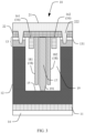
- FIG. 1 is a schematic diagram of a structure of a semiconductor device according to an embodiment of this application.
- the semiconductor device 10 includes a substrate 11.
- An epitaxial layer 12 and a semiconductor layer 13 are disposed on one side of the substrate 11, and a drain 14 is disposed on the other side of the substrate 11.
- the epitaxial layer 12 is located between the substrate 11 and the semiconductor layer 13.
- the semiconductor layer 13 includes a source region 131.
- the source region 131 is located on a side that is at the semiconductor layer 13 and that is away from the epitaxial layer 12.
- the semiconductor layer 13 is further provided with a trench 15.
- An opening of the trench 15 is located on a surface of a side that is of the source region 131 and that is away from the epitaxial layer 12.
- the trench 15 extends to the epitaxial layer 12 in a direction close to the substrate 11 (a vertical downward direction in FIG. 1 ). In other words, the trench 15 penetrates the semiconductor layer 13. It should be noted that a size of the opening of the trench 15 may not be specifically limited. In addition, an extension depth (the vertical direction in FIG. 1 ) of the trench 15 at the epitaxial layer 12 is not specifically limited.
- a gate 16, an electrode plate 17, and a shield gate structure 18 are disposed in the trench 15.
- the shield gate structure 18 includes a first shield gate 181 and a second shield gate 182.
- the first shield gate 181 and the second shield gate 182 are disposed on two sides of the electrode plate 17, and are spaced from the electrode plate 17.
- the gate 16 is disposed between the shield gate structure 18 and an inner wall of the trench 15, and is located on a side that is of the trench 15 and that is away from the substrate 11.
- the trench 15 is further provided with an oxidized layer structure 19.
- the oxidized layer structure 19 is filled between the shield gate structure 18 and the inner wall of the trench 15, between the shield gate structure 18 and the electrode plate 17, between the shield gate structure 18 and the gate 16, and between the gate 16 and the inner wall of the trench 15.
- the shield gate structure 18 and the electrode plate 17 may be spaced by using the oxidized layer structure 19, and electrode plate capacitance is formed.
- One of the source region 131, the gate 16, and the drain 14 is a first electrode, and one of the source region 131, the gate 16, and the drain 14 is a second electrode, and the first electrode is different from the second electrode.
- the electrode plate 17 may be electrically connected to the first electrode, and the shield gate structure 18 may be electrically connected to the second electrode.
- the source region 131 and the drain 14 may be separately electrically connected to the electrode plate capacitance.
- the gate 16 and the drain 14 may be separately electrically connected to the electrode plate capacitance.
- the gate 16 and the source region 131 may be separately electrically connected to the electrode plate capacitance.
- Output capacitance Coss, Miller capacitance Crss, or input capacitance Ciss may be separately adjusted by using the foregoing different structures.
- a value of the electrode plate capacitance is affected by the shield gate structure 18 and the electrode plate 17, in a process of fabricating the semiconductor device 10, a size and a position of the electrode plate 17 and a distance between the electrode plate 17 and the shield gate structure 18 may be adjusted. Therefore, the value of the electrode plate capacitance may be adjusted to adjust the capacitance of the semiconductor device 10. In this way, a turn-off stress of the semiconductor device 10 is reduced, and performance of the semiconductor device 10 is optimized.
- the electrode plate capacitance may be electrically connected to the source region 131 and the drain 14.
- the semiconductor device 10 further includes a source metal layer 21.
- the source metal layer 21 is disposed on the side that is at the semiconductor layer 13 and that is away from the epitaxial layer 12.
- the source metal layer 21 is connected to the source region 131 and the shield gate structure 18, to enable the source region 131 to be electrically connected to the shield gate structure 18 to form a source.
- the electrode plate capacitance is electrically connected to the source region 131.
- the oxidized layer structure 19 is provided with a contact hole 191.
- FIG. 2 is a schematic diagram of an equivalent capacitance network of the semiconductor device in FIG. 1 .
- electrode plate capacitance Cp is added between the source region 131 and the drain 14.
- An overlapping area between the source and the drain 14 that are of the semiconductor device 10 may be increased without affecting other electrical features such as a breakdown voltage and on-resistance that are of the semiconductor device 10, thereby increasing the output capacitance Coss and improving a non-linear feature of the output capacitance Coss.
- the output capacitance Coss includes Cds and the electrode plate capacitance Cp that are shown in FIG. 2 .
- a value of the electrode plate capacitance Cp is not affected by expansion of a depletion layer, so that a speed at which the output capacitance Coss decreases with a voltage can be reduced.
- the output capacitance Coss of the semiconductor device 10 may be changed by changing the value of the electrode plate capacitance Cp, thereby improving a switching feature and a resonance feature that are of the semiconductor device 10.
- the source metal layer 21 may be directly disposed on a surface of the source region 131, so that the source metal layer 21 is electrically connected to the source region 131.
- another functional layer may be disposed between the source metal layer 21 and the source region 131.
- the semiconductor device 10 may further include an insulation layer 22 disposed between the semiconductor layer 13 and the source metal layer 21.
- the insulation layer 22 is provided with a first via 221 and a second via 222.
- the first via 221 may be disposed on a surface of a side that is at the insulation layer 22 that is away from the semiconductor layer 13, and extends to the shield gate structure 18 in a direction towards the substrate 11.
- projection of the trench 15 in a direction perpendicular to the substrate 11 may cover projection of the first via 221 in the direction perpendicular to the substrate 11.
- the source metal layer 21 may be in contact with the shield gate structure 18 through the first via 221, so that the source metal layer 21 is electrically connected to the shield gate structure 18.
- the second via 222 may be disposed on the surface of the side that is at the insulation layer 22 that is away from the semiconductor layer 13, and extends to the source region 131 in the direction towards the substrate 11.
- projection of the source region 131 in the direction perpendicular to the substrate 11 may cover projection of the second via 222 in the direction perpendicular to the substrate 11.
- the source metal layer 21 may be in contact with the source region 131 through the second via 222, so that the source metal layer 21 is electrically connected to the source region 131.
- FIG. 3 is a schematic diagram of another structure of a semiconductor device according to an embodiment of this application.
- the electrode plate capacitance may be electrically connected to the gate 16 and the drain 14.
- the oxidized layer structure 19 is provided with a contact hole 191.
- the contact hole 191 extends to the epitaxial layer 12, to enable the electrode plate 17 to be electrically connected to the epitaxial layer 12 through the contact hole 191.
- the electrode plate capacitance is electrically connected to the drain 14.
- the semiconductor device 10 further includes an insulation layer 22.
- the insulation layer 22 is disposed on the side that is at the semiconductor layer 13 and that is away from the epitaxial layer 12.
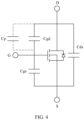
- FIG. 4 is a schematic diagram of an equivalent capacitance network of the semiconductor device in FIG. 3 . As shown in FIG. 4 , electrode plate capacitance Cp is added between the gate 16 and the drain 14.
- the Miller capacitance Crss includes Cgd and the electrode plate capacitance Cp that are shown in FIG. 4 .
- a value of the electrode plate capacitance Cp is not affected by expansion of a depletion layer, so that a speed at which the Miller capacitance Crss decreases with a voltage can be reduced.
- the Miller capacitance Crss of the semiconductor device 10 may be changed by changing the value of the electrode plate capacitance Cp, thereby improving a switching feature and a resonance feature that are of the semiconductor device 10.
- FIG. 5 is a schematic diagram of another structure of a semiconductor device according to an embodiment of this application.
- the electrode plate capacitance may be electrically connected to the gate 16 and the source region 131.
- the semiconductor device 10 further includes an insulation layer 22, a source metal layer 21, and a metal connecting wire (not shown in the figure).
- the insulation layer 22 is disposed on the side that is at the semiconductor layer 13 and that is away from the epitaxial layer 12. Both the source metal layer 21 and the metal connecting wire are disposed on a side that is at the insulation layer 22 and that is away from the semiconductor layer 13, and the source metal layer 21 and the metal connecting wire are spaced.
- FIG. 6 is a schematic diagram of an equivalent capacitance network of the semiconductor device in FIG. 5 . As shown in FIG. 6 , electrode plate capacitance is added between the gate 16 and the source region 131.
- An overlapping area between the gate 16 and a source that are of the semiconductor device 10 may be increased without affecting other electrical features such as a breakdown voltage and on-resistance that are of the semiconductor device 10, thereby increasing the input capacitance Ciss and improving a non-linear feature of the input capacitance Ciss.
- the input capacitance Ciss includes Cgs and the electrode plate capacitance Cp that are shown in FIG. 6 .
- a value of the electrode plate capacitance Cp is not affected by expansion of a depletion layer, so that a speed at which the input capacitance Ciss decreases with a voltage can be reduced.
- the input capacitance Ciss of the semiconductor device 10 may be changed by changing the value of the electrode plate capacitance Cp, thereby improving a switching feature and a resonance feature that are of the semiconductor device 10.
- a size and a position that are of the electrode plate 17, a distance between the electrode plate 17 and the shield gate structure 18, and the like may be adjusted to adjust the electrode plate capacitance.
- the electrode plate 17, the first shield gate 181, and the second shield gate 182 may be disposed in parallel, so that an electric field of the electrode plate capacitance is a uniform electric field. This facilitates adjustment of the value of the electrode plate capacitance.
- the electrode plate 17 may alternatively be non-parallel to the first shield gate 181 and the second shield gate 182. This is not specifically limited in this application.
- the electrode plate 17, the first shield gate 181, and the second shield gate 182 may be of plate-like structures.
- Projection of the electrode plate 17 in a direction perpendicular to the first shield gate 181 may fall on the first shield gate 181, and the projection overlaps a surface of a side that is of the first shield gate 181 and that is close to the electrode plate 17; and/or projection of the electrode plate 17 in a direction perpendicular to the second shield gate 182 may also fall on the second shield gate 182, and the projection overlaps a surface of a side that is of the second shield gate 182 and that is close to the electrode plate 17.
- the electrode plate 17, the first shield gate 181, and the second shield gate 182 may be disposed in parallel, and sizes of the electrode plate 17, the first shield gate 181, and the second shield gate 182 may be the same.
- the projection of the electrode plate 17 on the first shield gate 181 may overlap the surface of the first shield gate 181, and the projection of the electrode plate 17 on the second shield gate 182 may overlap the surface of the second shield gate 182.
- a first distance between the electrode plate 17 and the first shield gate 181, and a second distance between the electrode plate 17 and the second shield gate 182 may be adjusted to change the value of the electrode plate capacitance.
- a larger first distance and a larger second distance indicate a smaller value of the electrode plate capacitance.
- a smaller first distance and a smaller second distance indicate a larger value of the electrode plate capacitance. Therefore, in the process of fabricating the semiconductor device 10, the first distance and the second distance may be adjusted by controlling formation of the oxidized layer structure 19.
- types of the electrode plate 17, the first shield gate 181, and the second shield gate 182 may be the same or different. This is not specifically limited in this application.
- the electrode plate 17 may be a P-type shield electrode plate, and the first shield gate 181 and the second shield gate 182 may be P-type shield gates.
- the electrode plate 17 may be an N-type shield electrode plate, and the first shield gate 181 and the second shield gate 182 may be N-type shield gates.
- the electrode plate 17 may be a P-type shield electrode plate, and the first shield gate 181 and the second shield gate 182 may be N-type shield gates.
- the electrode plate 17 may be an N-type shield electrode plate, and the first shield gate 181 and the second shield gate 182 may be P-type shield gates.
- doping concentrations of the electrode plate 17 and the shield gate structure 18 may be the same, or may be different.
- the electrode plate 17 may be made of a same material or different materials as the first shield gate 181 and the second shield gate 182.
- the electrode plate 17, the first shield gate 181, and the second shield gate 182 may all use a polysilicon material, or may also use another conductive material such as tungsten or aluminum.
- the gate 16 may include a first gate 161 and a second gate 162.
- the first gate 161 is disposed between the first shield gate 181 and the inner wall of the trench 15, and the second gate 162 is disposed between the second shield gate 182 and the inner wall of the trench 15.
- the first gate 161 is disposed on a side that is of the first shield gate 181 and that is away from the electrode plate 17, and the second gate 162 is disposed on a side that is of the second shield gate 182 and that is away from the electrode plate 17.
- the first gate 161 When the electrode plate capacitance is added between the gate 16 and the drain 14, the first gate 161 may be electrically connected to the first shield gate 181 through the metal connecting wire, and the second gate 162 may be electrically connected to the second shield gate 182 through the metal connecting wire. In this way, the gate 16 is electrically connected to the electrode plate capacitance.
- the first electrode and the second electrode when the electrode plate capacitance is added between the gate 16 and the source, the first electrode and the second electrode may be separately electrically connected to the electrode plate 17 through the metal connecting wire. In this way, the gate 16 is electrically connected to the electrode plate capacitance.
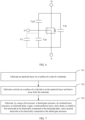
- FIG. 7 is a schematic flowchart of a method for preparing a semiconductor device according to an embodiment of this application. As shown in FIG. 7 , in this application, the method for fabricating the semiconductor device 10 may include the following steps.
- Step S701 Fabricate an epitaxial layer on a surface of a side of a substrate.
- Step S702 Fabricate a trench on a surface of a side that is at the epitaxial layer and that is away from the substrate.
- Step S703 Fabricate, by using a first process, a shield gate structure, an oxidized layer structure, an electrode plate, a gate, a semiconductor layer, and a drain, to enable a first electrode to be electrically connected to the electrode plate, and a second electrode to be electrically connected to the shield gate structure.
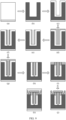
- FIG. 8 is a schematic diagram of a fabrication process of the semiconductor device in FIG. 1 .
- electrode plate capacitance is added between a drain and a source that are of the semiconductor device.
- a process of fabricating the semiconductor device may specifically include the following steps.
- step S8(e) the shield gate at the bottom of the trench is etched.
- a shield gate structure of a side wall of the trench is retained to form the first shield gate and the second shield gate.
- a specific value of the electrode plate capacitance may be adjusted by controlling sizes (for example, thickness, lengths, or heights) or positions (for example, positions relative to the first shield gate and the second shield gate) of the second oxidized layers, to adjust capacitance in the process of fabricating the semiconductor device.
- step S8(h) After step S8(h) is completed, the first oxidized layers and the second oxidized layers form an oxidized layer structure.
- the insulation layer may alternatively be omitted.
- FIG. 9 is a schematic diagram of a fabrication process of the semiconductor device in FIG. 3 .
- electrode plate capacitance is added between a drain and a gate that are of the semiconductor device.
- a process of fabricating the semiconductor device may specifically include the following steps.
- Step S9(a) to step S9(i) are the same as step S8(a) to step S8(i). Details are not described herein again.
- FIG. 10 is a schematic diagram of a fabrication process of the semiconductor device in FIG. 5 .
- electrode plate capacitance is added between a source and a gate that are of the semiconductor device.
- a process of fabricating the semiconductor device may specifically include the following steps.
- Step S 10(a) to step S 10(e) are the same as step S8(a) to step S8(e). Details are not described herein again.
- a specific value of the electrode plate capacitance may be adjusted by controlling sizes (for example, thickness, lengths, or heights) or positions (for example, positions relative to the first shield gate and the second shield gate) of the second oxidized layers, to adjust capacitance in the process of fabricating the semiconductor device.
- the insulation layer may alternatively be omitted.
- this application further provides an integrated circuit.
- the integrated circuit includes a circuit board and the semiconductor device in any one of the foregoing embodiments.
- the semiconductor device is disposed on the foregoing circuit board.
- a turn-off stress of the semiconductor device is low, and performance of the semiconductor device is good. Therefore, the semiconductor device can be applied to an application scenario of a circuit topology that has a specific requirement on a capacitance value, thereby improving system efficiency.
- a structure of the semiconductor device does not increase an area of the integrated circuit, and does not affect another parameter of the semiconductor device. Therefore, integration of the integrated circuit can be improved more effectively, and fabrication costs can be reduced.
- this application further provides an electronic device.
- the electronic device includes a housing and the foregoing integrated circuit, and the integrated circuit is disposed in the housing.
- the foregoing integrated circuit may be disposed inside or on a surface of the housing. This is not limited in this application. Capacitance of a semiconductor device can be adjusted, so that a turn-off stress of the semiconductor device is low, and performance of the semiconductor device is good. Therefore, the electronic device can work in an application scenario of a circuit topology that has a specific requirement on a capacitance value, thereby improving work efficiency.
- the integrated circuit has a high degree of integration. This facilitates miniaturization of the electronic device, and fabrication costs of the electronic device are low.
Landscapes
- Insulated Gate Type Field-Effect Transistor (AREA)
- Electrodes Of Semiconductors (AREA)
Applications Claiming Priority (2)
| Application Number | Priority Date | Filing Date | Title |
|---|---|---|---|
| CN202210260056.5A CN116799029A (zh) | 2022-03-16 | 2022-03-16 | 半导体器件及其制备方法、集成电路和电子设备 |
| PCT/CN2023/071647 WO2023173919A1 (zh) | 2022-03-16 | 2023-01-10 | 半导体器件及其制备方法、集成电路和电子设备 |
Publications (2)
| Publication Number | Publication Date |
|---|---|
| EP4407693A1 true EP4407693A1 (de) | 2024-07-31 |
| EP4407693A4 EP4407693A4 (de) | 2025-03-19 |
Family
ID=88022231
Family Applications (1)
| Application Number | Title | Priority Date | Filing Date |
|---|---|---|---|
| EP23769430.2A Pending EP4407693A4 (de) | 2022-03-16 | 2023-01-10 | Halbleiterbauelement und herstellungsverfahren dafür, integrierte schaltung und elektronische vorrichtung |
Country Status (4)
| Country | Link |
|---|---|
| US (1) | US20250006833A1 (de) |
| EP (1) | EP4407693A4 (de) |
| CN (1) | CN116799029A (de) |
| WO (1) | WO2023173919A1 (de) |
Families Citing this family (1)
| Publication number | Priority date | Publication date | Assignee | Title |
|---|---|---|---|---|
| CN118969793B (zh) * | 2024-10-17 | 2025-03-18 | 湖南三安半导体有限责任公司 | 半导体器件 |
Family Cites Families (6)
| Publication number | Priority date | Publication date | Assignee | Title |
|---|---|---|---|---|
| DE102004029435B4 (de) * | 2004-06-18 | 2017-02-16 | Infineon Technologies Ag | Feldplattentrenchtransistor |
| DE102005041285B4 (de) * | 2005-08-31 | 2009-06-25 | Infineon Technologies Ag | Grabenstrukturhalbleitereinrichtung und Verfahren zu deren Herstellung |
| CN102263133B (zh) * | 2011-08-22 | 2012-11-07 | 无锡新洁能功率半导体有限公司 | 低栅极电荷低导通电阻深沟槽功率mosfet器件及其制造方法 |
| US8796760B2 (en) * | 2012-03-14 | 2014-08-05 | Taiwan Semiconductor Manufacturing Company, Ltd. | Transistor and method of manufacturing the same |
| US9006820B2 (en) * | 2012-12-19 | 2015-04-14 | Alpha And Omega Semiconductor Incorporated | Vertical DMOS transistor |
| CN114188410A (zh) * | 2022-02-17 | 2022-03-15 | 绍兴中芯集成电路制造股份有限公司 | 屏蔽栅沟槽型功率mosfet器件 |
-
2022
- 2022-03-16 CN CN202210260056.5A patent/CN116799029A/zh active Pending
-
2023
- 2023-01-10 WO PCT/CN2023/071647 patent/WO2023173919A1/zh not_active Ceased
- 2023-01-10 EP EP23769430.2A patent/EP4407693A4/de active Pending
-
2024
- 2024-09-10 US US18/830,544 patent/US20250006833A1/en active Pending
Also Published As
| Publication number | Publication date |
|---|---|
| WO2023173919A1 (zh) | 2023-09-21 |
| CN116799029A (zh) | 2023-09-22 |
| EP4407693A4 (de) | 2025-03-19 |
| US20250006833A1 (en) | 2025-01-02 |
Similar Documents
| Publication | Publication Date | Title |
|---|---|---|
| CN101107718B (zh) | 功率金属氧化物半导体组件 | |
| CN100485961C (zh) | 具有增强的屏蔽结构的金属氧化物半导体器件 | |
| US8648445B2 (en) | Metal-oxide-semiconductor device having trenched diffusion region and method of forming same | |
| JP7698787B2 (ja) | 炭化珪素半導体装置及びその製造方法本願は、2021年11月17日中国特許庁に提出した、出願番号が202111363503.1、発明名称が「炭化珪素半導体装置及びその製造方法」である中国特許出願の優先権を要求し、その全ての内容が引用により本願に組み込まれる。本願は、2021年11月17日中国特許庁に提出した、出願番号が202122827400.8、発明名称が「炭化珪素半導体装置」である中国特許出願の優先権を要求し、その全ての内容が引用により本願に組み込まれる。 | |
| KR20220074921A (ko) | Ldmos 소자 및 이의 제조방법 | |
| KR101026953B1 (ko) | 자체 정렬된 구조를 갖는 수직 게이트 반도체 디바이스 | |
| TWI802048B (zh) | Ldmos電晶體及其製造方法 | |
| CN104638011B (zh) | 一种沟槽mosfet器件及其制作方法 | |
| US20250006833A1 (en) | Semiconductor device and preparation method thereof, integrated circuit, and electronic device | |
| CN102201450A (zh) | 一种隧穿场效应晶体管及其制备方法 | |
| CN111261702A (zh) | 沟槽型功率器件及其形成方法 | |
| WO2018098347A1 (en) | Method of forming a vertical field effect transistor with front-side source and drain contacts | |
| WO2023130798A1 (zh) | 碳化硅mosfet器件及其制作方法 | |
| CN106601811B (zh) | 沟槽式功率晶体管 | |
| US20180145171A1 (en) | Field Effect Transistor (FET) or Other Semiconductor Device with Front-Side Source and Drain Contacts | |
| CN106601795A (zh) | 一种沟槽式场效应晶体管及其制造方法 | |
| US8080457B1 (en) | Fabrication method of power semiconductor structure with low gate charge | |
| CN110828575A (zh) | 包括至少一个横向扩散场效应晶体管的半导体结构 | |
| CN106409888A (zh) | 沟槽式功率晶体管结构及其制造方法 | |
| CN116207149A (zh) | 半导体器件及其制作方法 | |
| CN115719759A (zh) | Ldmos器件及工艺方法 | |
| TWI435447B (zh) | 功率金氧半導體場效電晶體及其製造方法 | |
| CN117497408B (zh) | 一种hk-igbt及其制备方法、芯片 | |
| CN116666444A (zh) | Sgt器件的制备方法以及sgt器件 | |
| US6420756B1 (en) | Semiconductor device and method |
Legal Events
| Date | Code | Title | Description |
|---|---|---|---|
| STAA | Information on the status of an ep patent application or granted ep patent |
Free format text: STATUS: THE INTERNATIONAL PUBLICATION HAS BEEN MADE |
|
| PUAI | Public reference made under article 153(3) epc to a published international application that has entered the european phase |
Free format text: ORIGINAL CODE: 0009012 |
|
| STAA | Information on the status of an ep patent application or granted ep patent |
Free format text: STATUS: REQUEST FOR EXAMINATION WAS MADE |
|
| 17P | Request for examination filed |
Effective date: 20240423 |
|
| AK | Designated contracting states |
Kind code of ref document: A1 Designated state(s): AL AT BE BG CH CY CZ DE DK EE ES FI FR GB GR HR HU IE IS IT LI LT LU LV MC ME MK MT NL NO PL PT RO RS SE SI SK SM TR |
|
| REG | Reference to a national code |
Ref country code: DE Ref legal event code: R079 Free format text: PREVIOUS MAIN CLASS: H01L0029780000 Ipc: H10D0030010000 |
|
| A4 | Supplementary search report drawn up and despatched |
Effective date: 20250213 |
|
| RIC1 | Information provided on ipc code assigned before grant |
Ipc: H10D 64/27 20250101ALI20250207BHEP Ipc: H10D 64/20 20250101ALI20250207BHEP Ipc: H10D 30/66 20250101ALI20250207BHEP Ipc: H10D 30/01 20250101AFI20250207BHEP |
|
| DAV | Request for validation of the european patent (deleted) | ||
| DAX | Request for extension of the european patent (deleted) |