EP4404481A1 - Signaldetektionsvorrichtung, signaldetektionsverfahren und programm - Google Patents
Signaldetektionsvorrichtung, signaldetektionsverfahren und programm Download PDFInfo
- Publication number
- EP4404481A1 EP4404481A1 EP21957521.4A EP21957521A EP4404481A1 EP 4404481 A1 EP4404481 A1 EP 4404481A1 EP 21957521 A EP21957521 A EP 21957521A EP 4404481 A1 EP4404481 A1 EP 4404481A1
- Authority
- EP
- European Patent Office
- Prior art keywords
- signal
- optical
- frequency
- frequency conversion
- signal detection
- Prior art date
- Legal status (The legal status is an assumption and is not a legal conclusion. Google has not performed a legal analysis and makes no representation as to the accuracy of the status listed.)
- Pending
Links
Images


Classifications
-
- H—ELECTRICITY
- H04—ELECTRIC COMMUNICATION TECHNIQUE
- H04B—TRANSMISSION
- H04B10/00—Transmission systems employing electromagnetic waves other than radio-waves, e.g. infrared, visible or ultraviolet light, or employing corpuscular radiation, e.g. quantum communication
- H04B10/25—Arrangements specific to fibre transmission
- H04B10/2581—Multimode transmission
-
- H—ELECTRICITY
- H04—ELECTRIC COMMUNICATION TECHNIQUE
- H04B—TRANSMISSION
- H04B10/00—Transmission systems employing electromagnetic waves other than radio-waves, e.g. infrared, visible or ultraviolet light, or employing corpuscular radiation, e.g. quantum communication
- H04B10/60—Receivers
-
- H—ELECTRICITY
- H04—ELECTRIC COMMUNICATION TECHNIQUE
- H04J—MULTIPLEX COMMUNICATION
- H04J14/00—Optical multiplex systems
- H04J14/04—Mode multiplex systems
-
- H—ELECTRICITY
- H04—ELECTRIC COMMUNICATION TECHNIQUE
- H04J—MULTIPLEX COMMUNICATION
- H04J2203/00—Aspects of optical multiplex systems other than those covered by H04J14/05 and H04J14/07
Definitions
- the present invention relates to technologies for a signal detection device, a signal detection method, and a program.
- 5G fifth generation mobile communication system
- IoT Internet of Things
- a single mode fiber is used except for a local network for a short distance such as a local area network (LAN).
- the single mode fiber includes a single core serving as a path for an optical signal in the clad.
- the single mode fiber allows only single mode propagation in a wavelength band such as a C band (1528 to 1565 nm) or an L band (1570 to 1605 nm) used in a large-capacity long-distance optical network.
- a large-capacity long-distance optical network that stably transfers information that reaches several terabits per second over a long distance has been implemented.
- a digital coherent transmission technology using a digital signal processing technology and a coherent transmission/reception technology is introduced into an optical transmission device of a 100-gigabit-per-second class as a measure in an optical network against increasing communication traffic demand.
- the digital coherent transmission technology is a technology in which a coherent reception method and ultra-high-speed digital signal processing are combined.
- the coherent reception method is a reception method for detecting interference light between light on a reception side and local oscillation light.
- the ultra-high-speed digital signal processing is processing of digitizing a signal and then removing noise of a phase component caused by a frequency and phase fluctuation in a transmission side light source that generates signal light and a reception side light source that generates local oscillation light.
- a transmission method using the digital coherent transmission technology in an optical transmission system includes, for example, polarization-multiplexed optical transmission using two modes of orthogonal polarization for a single mode fiber.
- polarization-multiplexed optical transmission different pieces of information can be superimposed on polarization having an orthogonal relationship.
- mode-multiplexed optical transmission using a plurality of spatial modes hereinafter also referred to as "modes"
- mode-multiplexed optical transmission for example, a fiber having a core diameter expanded compared with that of a single mode fiber is used as a transmission medium.
- mode-multiplexed optical transmission a plurality of modes can be excited even in an existing wavelength band such as the C band, and different pieces of information can be superimposed on the respective modes and transmitted.
- mode-multiplexed optical signals are complicatedly mixed during propagation through a multimode optical fiber.
- a reception device that supports a mode diversity structure receives a mixed mode-multiplexed optical signal, converts the received mode-multiplexed optical signal into a digital signal, and performs separation using multiple-input and multiple-output (MIMO) digital signal processing of a scale corresponding to the number of modes to be excited.
- MIMO multiple-input and multiple-output
- a multi-mode fiber that excites two linearly polarized (LP) modes
- an LP01 mode that is a base mode and an LP11 mode that is a higher mode are excited.
- two modes of the LP11 mode (these are referred to as LP11a and LP11b) and polarization modes of each of the modes (these are referred to as X polarization and Y polarization) being utilized
- LP11a and LP11b polarization modes of each of the modes
- X polarization and Y polarization polarization and Y polarization
- different pieces of information can be superimposed on a total of six spatial modes of LP01X, LP01Y, LP11aX, LP11aY, LP11bX, and LP11bY. Therefore, if the nonlinear optical effect of an optical fiber is ignored, the multi-mode fiber for two LP modes can, in principle, achieve transmission capacity three times larger than that of an existing single mode fiber.
- Non Patent Literature 1 F. Hamaoka, S. Okamoto, K. Horikoshi, K. Yonenaga, A. Hirano and Y. Miyamoto, "Mode and polarization division multiplexed signal detection with single coherent receiver using mode-selective coherent detection technique,"2016 Optical Fiber Communications Conference and Exhibition (OFC), Th3A.6 (2016 )
- the number of components in a transceiver device increases according to the number of used spatial modes.
- the number of required components and elements including a digital-to-analog converter that converts a digital signal in an optical transceiver device into an analog signal, an analog-to-digital converter that converts an analog signal into a digital signal, a driver amplifier, an optical modulator, a reception optical front end, a semiconductor optical amplifier, a photodetector, and a feedback monitor, and the like is required to be at least three times larger as compared with a system in which an existing single mode fiber is the transmission medium.
- the footprint and power consumption of an optical transceiver device included in an optical transceiver increase, and the device manufacturing cost increases due to a change in a manufacturing process of an integrated component.
- Non Patent Literature 1 As a means for reducing the number of receiver components and elements in a mode-multiplexed transmission system, for example, a mode selection coherent detection technology described in Non Patent Literature 1 has been proposed. In the technology described in Non Patent Literature 1, there is an issue that a mode multiplexer for locally generated light and a mechanism for generating synchronous light need to be provided in a form of being added for each wavelength channel, and an effect of reducing the number of components and the number of elements of the entire communication system is limited.
- an object of the present invention is to provide a technology capable of reducing the number of components in a reception device in a transmission system to which the space-division multiplexing transmission technology is applied.
- One aspect of the present invention is a signal detection device including, a mode demultiplexer configured to convert N (N is a natural number) spatial mode signals including a plurality of higher modes excited in a transmission path fiber into N base modes and output the N basis modes, a frequency conversion unit configured to convert frequencies of respective N optical signals into frequencies different from each other, a multiplexing unit configured to multiplex the N optical signals having frequencies that have been converted, and a reception unit configured to photoelectrically convert a multiplexed optical signal while maintaining modulation information for a phase and polarization, perform digital signal conversion and signal processing, and demodulate an original information sequence.
- N is a natural number
- One aspect of the present invention is a signal detection method performed by a signal detection device including, converting N (N is a natural number) spatial mode signals including a plurality of higher modes excited in a transmission path fiber into N base modes and outputting the N basis modes, converting frequencies of respective N optical signals into frequencies different from each other, multiplexing the N optical signals having frequencies that have been converted, and photoelectrically converting a multiplexed optical signal while maintaining modulation information for a phase and polarization, performing digital signal conversion and signal processing, and demodulating an original information sequence.
- N is a natural number
- One aspect of the present invention is a program for causing a computer to function as the above signal detection device.
- the number of components in a reception device can be reduced in a transmission system to which the space-division multiplexing transmission technology is applied.
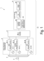
- Fig. 1 is a diagram showing a configuration example of a signal detection system according to the present embodiment.
- a signal detection system 1 includes a signal detection device 10 and an optical transmission fiber 2.
- the signal detection device 10 includes a mode demultiplexer 3, space-frequency conversion unit 4 (frequency conversion unit), an N ⁇ 1 optical coupler 5 (combiner) (multiplexing unit), and a reception unit 6.
- the space-frequency conversion unit 4 includes, for example, N (N is an integer of 1 or more) clock units 41 (first clock unit 41-1, second clock unit 41-2,..., Nth clock unit 41-N) and N frequency shifters 42 (first frequency shifter 42-1, second frequency shifter 42-2,..., Nth frequency shifter 42-N).
- the reception unit 6 includes, for example, a light locally reception unit 61, a coherent receiver 62, an AD converter 64, and a signal processing unit 65.
- Fig. 1 the configuration shown in Fig. 1 is an example, and the configuration is not limited thereto.
- the signal detection device 10 demodulates a signal sequence transmitted from the transmission side without an error in information by converting an optical signal propagated through the transmission path fiber 2 into a digital signal through photoelectric conversion, and then performing various types of signal processing.
- the transmission path fiber 2 is, for example, a spatial multiplexing fiber capable of exciting a plurality of spatial modes in a predetermined optical communication band, such as a multimode fiber.
- the mode demultiplexer 3 converts N spatial mode signals including a plurality of higher modes excited in the transmission path fiber 2 into N base modes and outputs the N base modes.
- the space-frequency conversion unit 4 converts the frequency of each optical signal.
- the space-frequency conversion unit 4 converts the frequencies of respective N optical signals into frequencies different from each other.
- the space-frequency conversion unit 4 performs frequency conversion by frequency-shifting each of the optical signals.
- Each of the N clock units 41 generates and outputs a clock signal having a frequency f.
- the N clock units are desirably synchronized by a means such as an external clock for synchronization from the viewpoint of reducing a load on the signal processing unit, but the N clock units may not necessarily be synchronized.
- Optical signal outputs from the mode demultiplexer 3 and clock signals from the clock units 41 are input to the N frequency shifters 42.
- the nth (n is one of 1 to N) frequency shifter 42-n gives a frequency shift amount of n ⁇ f to an optical signal. That is, the first frequency shifter 42-1 gives a frequency shift amount of ⁇ f, and the second frequency shifter 42-2 gives a frequency shift amount of 2 ⁇ f to an optical signal.
- the frequency shift in the frequency shifters 42 can be implemented by, for example, a Mach-Zehnder type optical modulator including a lithium niobate based waveguide using an electro-optical effect (for example, Reference Literature 1), but is not limited thereto as long as it has a function of a predetermined frequency shift.
- a Mach-Zehnder type optical modulator including a lithium niobate based waveguide using an electro-optical effect for example, Reference Literature 1
- Reference Literature 1 an electro-optical effect
- Reference Literature 1 M. Izutsu, S. Shikama, and T. Sueta, "Integrated optical SSB modulator/frequency shifter," IEEE J. Quantum Electron. 17(11), 2225-2227 (1981 ).
- the N ⁇ 1 optical coupler 5 multiplexes and outputs optical signals output from the frequency shifters.
- the N ⁇ 1 optical coupler may be, for example, a combiner that couples a plurality of laser beams to one fiber.
- the reception unit 6 decodes signals by mixing received signal light and locally generated light and outputs the signals to, for example, an external device.
- the light locally reception unit 61 includes, for example, a laser diode as a light source, and emits and outputs locally received light.
- the coherent receiver 62 includes, for example, a phase and polarization diversity configuration.
- the coherent receiver 62 performs conversion into analog electrical signals by photoelectric conversion while maintaining modulation information for a phase and polarization by received and multiplexed reception signals and locally generated light input.
- the AD converter 64 converts the analog electrical signals into digital signals by sampling processing.
- the signal processing unit 65 performs predetermined signal processing including, for example, waveform distortion removal, MIMO type signal processing, frequency offset compensation, phase noise compensation, error correction decoding, and the like, and demodulates the original correct information sequence (symbol sequence or binary sequence).
- Fig. 2 is a diagram showing optical spectra of an input unit and an output unit of an optical signal of an N ⁇ 1 optical coupler according to the present embodiment.
- signals input to the N ⁇ 1 optical coupler 5 are subjected to a frequency shift of n ⁇ f as compared with an original carrier wave frequency f c by the respective frequency shifters 42.
- the N ⁇ 1 optical coupler 5 multiplexes n optical signals (g11 to g13) to obtain optical signals arranged on the frequency axis at intervals of ⁇ f like an optical spectrum g14.
- Fig. 3 is a flowchart of a processing procedure example of a signal detection device according to the present embodiment.
- Step S1 The mode demultiplexer 3 converts N spatial mode signals including a plurality of higher modes excited in the transmission path fiber 2 into N base modes.
- Step S2 The nth frequency shifter 42-n converts the frequency of an optical signal by giving a frequency shift amount of n ⁇ f to an optical signal.
- Step S3 The N ⁇ 1 optical coupler 5 multiplexes optical signals output from the respective frequency shifters 42.
- Step S4 The coherent receiver 62 performs conversion into analog electrical signals by photoelectric conversion while maintaining modulation information for a phase and polarization by reception signals and locally generated light input.
- Step S5 The AD converter 64 converts the analog electrical signals into digital signals by sampling processing.
- the signal processing unit 65 performs predetermined signal processing including, for example, waveform distortion removal, MIMO type signal processing, frequency offset compensation, phase noise compensation, error correction decoding, and the like, and demodulates the original correct information sequence.
- N spatial modes are received by the single reception unit 6 using the transmission path fiber by locally generated light being mixed with output signals of the N ⁇ 1 optical coupler 5 and photoelectric conversion by intradyne coherent detection or heterodyne coherent detection being performed by a photodetector, so that the number of components in the signal detection device 10 can be reduced.
- one reception unit 6 is sufficient for implementation. Even in a digital domain digitally obtained by converting by the AD converter 64, reception signals are arranged with frequency intervals of ⁇ f being maintained on the frequency axis under a condition that the sampling theorem in which aliasing does not occur is satisfied. Furthermore, according to the present embodiment, one reception unit 6 can obtain a reception signal sequence equivalent to signals received by N reception units of the conventional configuration under a condition that the sampling speed limitation of the AD converter 64 and the band limitation of each device can be ignored by a frequency shift of -n ⁇ f being performed on the obtained nth signal by digital signal processing and the nth signal being converted into a baseband signal.
- the reception method may be a direct reception form in which locally generated light is not used.
- N spatial modes may be divided into p groups (p is an integer of 1 or more and N or less), and p configurations that perform reception by the reception function unit after a predetermined frequency shift and multiplexing may be arranged in parallel.
- p is a number determined by the bandwidth and the required cost of configuration devices of the reception unit 6, and at this time, an effect of reducing reception units 6 corresponds to 1/p in the number of the entire reception units as compared with the conventional configuration.
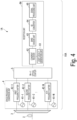
- Fig. 4 is a diagram showing a configuration example of a signal detection system according to the present embodiment.
- a signal detection system 1A includes a signal detection device 10A and an optical transmission fiber 2.
- the signal detection device 10A includes a mode demultiplexer 3, a space-frequency conversion unit 4 (frequency conversion unit), an N ⁇ 1 optical coupler 5 (multiplexing unit), and a reception unit 6A.
- the reception unit 6A includes, for example, a light locally reception unit 61, a coherent receiver 62, a band division unit 63, an AD converter 64, and a signal processing unit 65.
- Fig. 4 is an example, and the configuration is not limited thereto.
- the space-frequency conversion unit 4 converts the frequency of each optical signal.
- the space-frequency conversion unit 4 similarly to the first embodiment, performs frequency conversion by frequency-shifting each optical signal.
- the band division unit 63 outputs analog electrical signals to the AD converter 64 as a plurality of parallelized signals.
- the function of band division of the band division unit 63 means, for example, that analog electrical signals are divided into high frequency and low frequency side bands, and the center of each side band is converted into a frequency corresponding to a DC component and output, and can be implemented by, for example, a broadband circuit mounting technology as indicated in Reference Literature 2.
- analog electrical signals obtained by photoelectrically converting by the coherent receiver 62 are arranged on the frequency axis at frequency intervals of ⁇ f by respective frequency shifters.
- Fig. 5 is a flowchart of a processing procedure example of a signal detection device according to the present embodiment.
- Step S1 The mode demultiplexer 3 converts N spatial mode signals including a plurality of higher modes excited in the transmission path fiber 2 into N base modes.
- Step S2 The nth frequency shifter 42-n converts the frequency of an optical signal by giving a frequency shift amount of n ⁇ f to an optical signal.
- Step S3 The N ⁇ 1 optical coupler 5 multiplexes optical signals output from the respective frequency shifters 42.
- Step S4 The coherent receiver 62 performs conversion into analog electrical signals by photoelectric conversion while maintaining modulation information for a phase and polarization by reception signals and locally generated light input.
- the band division unit 63 outputs the analog electrical signals to the AD converter 64 as a plurality of parallelized signals.
- Step S5 The AD converter 64 converts the analog electrical signals into digital signals by sampling processing.
- the signal processing unit 65 performs predetermined signal processing including, for example, waveform distortion removal, MIMO type signal processing, frequency offset compensation, phase noise compensation, error correction decoding, and the like, and demodulates the original correct information sequence.
- the reception unit 6A further includes the band division unit 63, the highest frequencies included in analog electrical signals are reduced, and requirement conditions of the band limitation and the operation frequency limitation on an electric circuit and a digital circuit in the subsequent stage can be expected to be loosened.
- the band division unit may have a function of converting an input of a single analog electrical signal into q (q is an integer of 1 or more and N or less) low-speed output signals. That is, the band division unit 63 may perform digital signal processing and signal processing after performing division into parallel signals including a plurality of signal bands.
- Fig. 6 is a diagram showing a configuration example of a signal detection system according to the present embodiment.
- a signal detection system 1B includes a signal detection device 10B and an optical transmission fiber 2.
- the signal detection device 10B includes a mode demultiplexer 3, a space-frequency conversion unit 4B (frequency conversion unit), an N ⁇ 1 optical coupler 5 (multiplexing unit), and a reception unit 6.
- the space-frequency conversion unit 4B includes, for example, N clock units 41 (first clock unit 41-1, second clock unit 41-2,..., Nth clock unit 41-N), 2N frequency shifters 42 (first frequency shifter 42-1-1, first frequency shifter 42-1-2, second frequency shifter 42-2-1, second frequency shifter 42-2-2,..., Nth frequency shifter 42-N-1, Nth frequency shifter 42-N-2), polarized light beam splitters 43 (43-1, 43-2,..., 43-N), and polarized light beam combiners 44 (44-1, 44-2,..., 44-N).
- N clock units 41 first clock unit 41-1, second clock unit 41-2,..., Nth clock unit 41-N
- 2N frequency shifters 42 first frequency shifter 42-1-1, first frequency shifter 42-1-2, second frequency shifter 42-2-1, second frequency shifter 42-2-2,..., Nth frequency shifter 42-N-1, Nth frequency shifter 42-N-2
- polarized light beam splitters 43 43-1, 43-2,..., 43-N
- Fig. 6 is an example, and the configuration is not limited thereto.
- the space-frequency conversion unit 4B converts the frequency of each optical signal.
- the space-frequency conversion unit 4 performs frequency conversion by frequency-shifting each optical signal for each change, and outputs signals obtained by the conversion.
- the space-frequency conversion unit 4B includes two frequency shifters 42-n-1, 2 for each optical signal sequence.
- a polarization beam splitter 43 is connected to each input of the two frequency shifters 42-n-1, and a polarization beam combiner 44 is connected to each output of the two frequency shifters.
- An optical modulator that implements frequency shift is generally a waveguide type, and thus has polarization dependency for input light. Therefore, in the present embodiment, the polarization beam splitters 43 or the polarization beam combiners 44 are provided before and after the input of the frequency shifters 42, and polarization diversity is achieved to enable support for a polarization multiplexed signal.
- the polarization beam splitters 43 are optical elements, and separate each optical signal output from the mode demultiplexer 3 into S-polarized light and P-polarized light.
- the nth frequency shifter 42-n-1 gives a frequency shift amount of n ⁇ f to the S-polarized light.
- the nth frequency shifter 42-n-2 converts the frequency of an optical signal by giving a frequency shift amount of n ⁇ f to the P-polarized light.
- the polarization beam combiners 44 are optical elements, multiplex an optical signal output from the nth frequency shifter 42-n-1 and an optical signal output from the nth frequency shifter 42-n-2, and output the multiplexed signals to the N ⁇ 1 optical coupler 5.
- Fig. 7 is a flowchart of a processing procedure example of a signal detection device according to the present embodiment.
- Step S1 The mode demultiplexer 3 converts N spatial mode signals including a plurality of higher modes excited in the transmission path fiber 2 into N base modes.
- Step S21 The polarization beam splitters 43 separate each optical signal output from the mode demultiplexer 3 into S-polarized light and P-polarized light.
- the frequency shifters 42 convert the frequencies of optical signals by giving a frequency shift amount of ⁇ f to the S-polarized light or the P-polarized light.
- the polarization beam combiners 44 are optical elements, and multiplex an optical signal output from the nth frequency shifter 42-n-1 and an optical signal output from the nth frequency shifter 42-n-2.
- Step S3 The N ⁇ 1 optical coupler 5 multiplexes optical signals output from the respective frequency shifters 42.
- Step S4 The coherent receiver 62 performs conversion into analog electrical signals by photoelectric conversion while maintaining modulation information for a phase and polarization by reception signals and locally generated light input.
- Step S5 The AD converter 64 converts the analog electrical signals into digital signals by sampling processing.
- the signal processing unit 65 performs predetermined signal processing including, for example, waveform distortion removal, MIMO type signal processing, frequency offset compensation, phase noise compensation, error correction decoding, and the like, and demodulates the original correct information sequence.
- the polarization beam splitters 43 or the polarization beam combiners 44 are provided before and after the input of the frequency shifters 42, and a frequency shift amount is given to each piece of polarized light.
- polarization diversity can be achieved and a polarization multiplexed signal can be supported.
- reception unit 6 may be the reception unit 6B of the second embodiment including the band division unit 63.
- a space-frequency conversion unit collectively processes wavelength division multiplexing (WDM) signals in which optical signals of respective spatial modes propagated through an optical transmission fiber 2 each include K (K is an integer of 1 or more) wavelength multiplexed signals.
- WDM wavelength division multiplexing
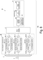
- Fig. 8 is a diagram showing a configuration example of a signal detection system according to the present embodiment.
- a signal detection system 1C includes a signal detection device 10C and the optical transmission fiber 2.
- the signal detection device 10C includes a mode demultiplexer 3, a space-frequency conversion unit 4C (frequency conversion unit), K N ⁇ 1 optical couplers 5 (multiplexing unit) (N ⁇ 1 optical coupler 5-1,..., N ⁇ 1 optical coupler 5-K), and K reception units 6 (reception unit 6-1,..., reception unit 6-K).
- the space-frequency conversion unit 4C includes, for example, N (N is an integer of 1 or more) clock units 41 (first clock unit 41-1, second clock unit 41-2,..., Nth clock unit 41-N), N frequency shifters 42 (first frequency shifter 42-1, second frequency shifter 42-2,..., Nth frequency shifter 42-N), and WDM demultiplexers 45 (WDM demultiplexer 45-1, WDM demultiplexer 45-2,..., WDM demultiplexer 45-N).
- Fig. 8 is an example, and the configuration is not limited thereto.
- the space-frequency conversion unit 4C converts the frequency of each optical signal.
- the space-frequency conversion unit 4C frequency-shifts each optical signal to convert the frequency of the optical signal, and the WDM demultiplexers 45 further perform demultiplexing for each channel.
- the nth frequency shifter 42-n converts the frequency of an optical signal by collectively giving a frequency shift amount of n ⁇ f to K WDM wavelength channels.
- the WDM demultiplexers 45 demultiplex K WDM wavelength channels for each of the channels.
- the N ⁇ 1 optical couplers 5 multiplex and output output signals for each of the wavelength channels.
- the K reception units 6 perform reception processing and demodulation processing on the wavelength channels by a means similar to the first embodiment.
- Fig. 9 is a diagram showing a connection relationship between WDM demultiplexers and K N ⁇ 1 optical couplers of a space-frequency conversion unit according to the present embodiment.
- first channel signals of the respective WDM demultiplexers 45-1 to 45-N are input to the N ⁇ 1 optical coupler 5-1
- second channel signals of the respective WDM demultiplexers 45-1 to 45-N are input to the N ⁇ 1 optical coupler 5-2,...
- K-th channel signals of the respective WDM demultiplexers 45-1 to 45-N are input to the N ⁇ 1 optical coupler 5-K.
- Fig. 10 is a flowchart of a processing procedure example of a signal detection device according to the present embodiment.
- Step S1 The mode demultiplexer 3 converts N spatial mode signals including a plurality of higher modes excited in the transmission path fiber 2 into N base modes.
- the nth frequency shifter 42-n converts the frequency of an optical signal by collectively giving a frequency shift amount of n ⁇ f to K WDM wavelength channels.
- Step S32 The WDM demultiplexers 45 demultiplex K WDM wavelength channels for each of the channels.
- Step S33 The N ⁇ 1 optical couplers 5 multiplex output signals for each of the wavelength channels in optical signals to which the frequency shift amount has been given.
- Step S4 The coherent receiver 62 performs conversion into analog electrical signals by photoelectric conversion while maintaining modulation information for a phase and polarization by reception signals and locally generated light input.
- Step S5 The AD converter 64 converts the analog electrical signals into digital signals by sampling processing.
- the signal processing unit 65 performs predetermined signal processing including, for example, waveform distortion removal, MIMO type signal processing, frequency offset compensation, phase noise compensation, error correction decoding, and the like, and demodulates the original correct information sequence.
- the space-frequency conversion unit 4C includes the WDM demultiplexers 45 at the subsequent stage of the respective frequency shifters 42, and output signals for each wavelength channel are multiplexed by the N ⁇ 1 optical couplers 5 at the subsequent stage.
- the K reception units 6 perform reception processing and demodulation processing on the wavelength channels by a means similar to the first embodiment.
- K WDM wavelength channels can be frequency-shifted collectively, and a WDM configuration in which optical signals of respective spatial modes propagated through a transmission path fiber each include K wavelength multiplex signals can be supported.
- K space-frequency conversion units 4 (or 4A, 4B) need to be included.
- the number of space-frequency conversion units can be 1/K times as compared with the first to third embodiments in which each WDM wavelength channel is frequency-shifted.
- each of the reception units 6 may be the reception unit 6B of the second embodiment including the band division unit 63.
- the present embodiment is a configuration example in which the frequency shifters 42 in the space-frequency conversion unit 4C of the fourth embodiment are replaced with frequency conversion units 46.
- Fig. 11 is a diagram showing a configuration example of a signal detection system according to the present embodiment.
- a signal detection system 1D includes a signal detection device 10D and an optical transmission fiber 2.
- the signal detection device 10D includes a mode demultiplexer 3, a space-frequency conversion unit 4D (frequency conversion unit), K N ⁇ 1 optical couplers 5 (multiplexing unit), and K reception units 6 (reception unit 6-1, reception unit 6-2..., reception unit 6-K).
- the space-frequency conversion unit 4D includes, for example, N (N is an integer of 1 or more) frequency conversion units 46 (first frequency conversion unit 46-1, second frequency conversion unit 46-2,..., Nth frequency conversion unit 46-N) and WDM demultiplexers 45 (WDM demultiplexer 45-1, WDM demultiplexer 45-2,..., WDM demultiplexer 45-N).
- Fig. 11 is an example, and the configuration is not limited thereto.
- the space-frequency conversion unit 4D converts the frequency of each optical signal.
- the frequency conversion units 46 wavelength-convert optical signals to convert the frequencies of the optical signals, and the WDM demultiplexers 45 further perform demultiplexing for each channel.
- the frequency conversion units 46 convert the frequencies of the optical signals by performing wavelength conversion on K WDM wavelength channels. For example, excitation light of 2f c + n ⁇ f is also input to the nth frequency conversion unit 46-n.
- a nonlinear optical effect using a highly nonlinear fiber for example, a periodically poled lithium niobate (PPLN), a semiconductor optical amplifier, a silicon waveguide, or the like can be used.
- Fig. 12 is a diagram showing states of transition of optical spectra before and after frequency conversion in a first frequency conversion unit to an Nth frequency conversion unit in a space-frequency conversion unit according to the present embodiment.
- transition diagrams g201 to g203 of the optical spectra the horizontal axis represents the frequency.
- K WDM signals are input to the space-frequency conversion unit 4D as input light.
- the original K WDM signals generate output light (idler light) that appears as if it is folded back around a frequency of f c + n ⁇ /2 (hereinafter, this is referred to as a center frequency) as a target axis by a non-degenerate optical parametric process of the excitation light and input light as shown in the transition diagrams g201 to g203 of the optical spectra in Fig. 12 .
- WDM signals generated in the space-frequency conversion unit 4D can obtain output light shifted by ⁇ f.
- wavelength channels to the reception units 6 each have a phase conjugate relationship as compared with an optical signal originally transmitted from the transmission side.
- adjustment by the optical path length in the phase diversity configuration inside the coherent receiver or phase conjugate inversion processing in the digital signal processing unit can be used.
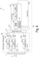
- Fig. 13 is a diagram showing a configuration example of the space-frequency conversion unit according to the present embodiment.
- the space-frequency conversion unit 4D includes, for example, a light source 401, a frequency comb generation unit 402, a 1 ⁇ N optical splitter 403, N optical filters 404 (404-1, 404-2,..., 404-N), N optical amplifiers 405 (405-1, 405-2,..., 405-N), N optical filters 406 (406-1, 406-2,..., 406-N), N PPLNs 407 (407-1, 407-2,..., 407-N), and N frequency conversion units 46 (first frequency conversion unit 46-1,..., Nth frequency conversion unit 46-N).
- the light source 401 outputs continuous light as seed light of excitation light to the frequency comb generation unit 402.
- the frequency comb generation unit 402 generates a frequency comb in which arrangement is performed at frequency intervals of ⁇ f using the continuous light, and outputs the generated frequency comb to the 1 ⁇ N optical splitter 403.
- a method of generating a frequency comb for example, there are a configuration using a plurality of intensity modulators and a configuration using a mode-locked laser, but the method is not limited thereto.
- the 1 ⁇ N optical splitter 403 splits the frequency comb into N frequency combs and outputs the frequency combs to the respective optical filters 404 (404-1, 404-2,..., 404-N).
- the optical filters 404 (404-1, 404-2,..., 404-N) perform filter processing on input optical signals and output the optical signals to the optical amplifiers 405 (405-1, 405-2,..., 405-N) corresponding to the optical filters 404.
- the optical amplifiers 405 (405-1, 405-2,..., 405-N) perform amplification processing on the optical signals on which the filtering processing has been performed and output the optical signals to the optical filters 406 (406-1, 406-2,..., 406-N) corresponding to the optical amplifiers 405.
- the optical filters 406 (406-1, 406-2,..., 406-N) perform filter processing on the input optical signals and output the optical signals to the PPLNs 407 (407-1, 407-2,..., 407-N) corresponding to the optical filters 406.
- the PPLNs 407 (407-1, 407-2,..., 407-N) generate second harmonic waves for the input optical signals and output the second harmonic waves to the frequency conversion units 46 (first frequency conversion unit 46-1,..., Nth frequency conversion unit 46-N) corresponding to the PPLNs 407.
- the PPLN 407-1 outputs an optical signal of 2f c + ⁇ f to the first frequency conversion unit 46-1,...
- the PPLN 407-N outputs an optical signal of 2fc + N ⁇ f to the Nth frequency conversion unit 46-N.
- the space-frequency conversion unit 4D obtains N pieces of excitation light arranged at frequency intervals of ⁇ f from 2f c + ⁇ f to 2f c + N ⁇ f.
- the space-frequency conversion unit 4D can obtain output light that appears as if it is folded back around the center frequency as an axis.
- the configuration shown in Fig. 13 is an example, and the configuration is not limited thereto.
- a method of performing collective generation through frequency comb generation is exemplified as a method of generating N pieces of excitation light, but the present invention is not limited thereto.
- N pieces of excitation light may be independently generated using N individual light sources.
- Fig. 14 is a flowchart of a processing procedure example of a signal detection device according to the present embodiment.
- Step S1 The mode demultiplexer 3 converts N spatial mode signals including a plurality of higher modes excited in the transmission path fiber 2 into N base modes.
- the frequency conversion units 46 convert the frequencies of the optical signals by performing wavelength conversion on K WDM wavelength channels.
- the WDM demultiplexers 45 demultiplex the K WDM wavelength channels for each of the channels.
- Step S43 The N ⁇ 1 optical couplers 5 multiplex output signals for each of the wavelength channels in the frequency-converted and demultiplexed optical signals.
- Step S4 The coherent receiver 62 performs conversion into analog electrical signals by photoelectric conversion while maintaining modulation information for a phase and polarization by reception signals and locally generated light input.
- Step S5 The AD converter 64 converts the analog electrical signals into digital signals by sampling processing.
- the signal processing unit 65 performs predetermined signal processing including, for example, waveform distortion removal, MIMO type signal processing, frequency offset compensation, phase noise compensation, error correction decoding, and the like, and demodulates the original correct information sequence.
- the frequency shifters in the space-frequency conversion unit of the fourth embodiment are replaced with the frequency conversion units 46.
- the electric band limitation of frequency shift amounts in the frequency shifters can be avoided and the shift conversion efficiency (extinction ratio) can be improved.
- each of the reception units 6 may be the reception unit 6B of the second embodiment including the band division unit 63.
- the present embodiment is an example in which an operation band of a device in a transmission band is not changed.
- Fig. 15 is a diagram showing a configuration example of a signal detection system according to the present embodiment.
- a signal detection system 1E includes a signal detection device 10E and an optical transmission fiber 2.
- the signal detection device 10E includes a mode demultiplexer 3, a space-frequency conversion unit 4E (frequency conversion unit), K N ⁇ 1 optical couplers 5 (multiplexing unit), and K reception units 6 (reception unit 6-1, reception unit 6-2..., reception unit 6-K).
- the space-frequency conversion unit 4E includes, for example, N (N is an integer of 1 or more) frequency conversion units 46 (first frequency conversion unit 46-1-1, second frequency conversion unit 46-2-1,..., Nth frequency conversion unit 46-N-1), N frequency conversion units 47 (first frequency conversion unit 47-1-1, second frequency conversion unit 47-2-1,..., Nth frequency conversion unit 47-N-1), and WDM demultiplexers 45 (WDM demultiplexer 45-1, WDM demultiplexer 45-2,..., WDM demultiplexer 45-N).
- N is an integer of 1 or more frequency conversion units 46 (first frequency conversion unit 46-1-1, second frequency conversion unit 46-2-1,..., Nth frequency conversion unit 46-N-1), N frequency conversion units 47 (first frequency conversion unit 47-1-1, second frequency conversion unit 47-2-1,..., Nth frequency conversion unit 47-N-1), and WDM demultiplexers 45 (WDM demultiplexer 45-1, WDM demultiplexer 45-2,..., WDM demultiplexer 45-N).
- Fig. 15 is an example, and the configuration is not limited thereto.
- the nth frequency conversion unit 47-n-1 is connected in series after the nth frequency conversion unit 46-n-1, and the output of the nth frequency conversion unit 47-n-1 is connected to the input of the WDM demultiplexer 45-n.
- the space-frequency conversion unit 4E converts the frequency of each optical signal.
- the frequency conversion units 46 frequency-convert each optical signal, the frequency conversion units 47 perform frequency-conversion again, and then the WDM demultiplexers 45 further perform demultiplexing for each channel.
- the frequency conversion units 46 convert the frequencies of optical signals by performing wavelength conversion on K WDM wavelength channels, and output the optical signals obtained by the conversion to the frequency conversion units 47 connected in series to the frequency conversion units 46.
- the frequency conversion units 47 convert the frequencies of the optical signals by performing wavelength conversion on the input optical signals, and output the optical signals obtained by the conversion to the WDM demultiplexers 45 connected to the frequency conversion units 47.
- output light from the frequency conversion units 46 is phase conjugate light folded back around the center frequency as an axis.
- This qualitatively means that output light is generated at a position more distant on the frequency axis than input light as the output light is more distant on the frequency axis from the center frequency and as the number K of WDM signal channels is larger. Therefore, there is concern that a new transmission band in which output light is located is outside the operation band of each element inside the reception unit.
- frequency conversion units are arranged in series and frequency conversion is continuously performed, so that input light and output light of the frequency conversion units can be handled in the same transmission bands.
- the frequency of each piece of excitation light is set under a condition that, for input light located at a frequency of f c , output light satisfies a frequency of f c + n ⁇ f by the nth frequency conversion unit 47 of the subsequent stage (first frequency conversion unit 47-1-1, second frequency conversion unit 47-2-1,..., Nth frequency conversion unit 47-N-1).
- Fig. 16 is a flowchart of a processing procedure example of a signal detection device according to the present embodiment.
- Step S1 The mode demultiplexer 3 converts N spatial mode signals including a plurality of higher modes excited in the transmission path fiber 2 into N base modes.
- Step S41 The frequency conversion units 46 perform wavelength conversion on K WDM wavelength channels.
- the frequency conversion units 47 perform conversion of the frequencies of optical signals by performing wavelength conversion on the optical signals on which the wavelength conversion has been performed.
- the WDM demultiplexers 45 demultiplex the K WDM wavelength channels for each of the channels.
- Step S43 The N ⁇ 1 optical couplers 5 multiplex output signals for each of the wavelength channels in the frequency-converted and demultiplexed optical signals.
- Step S4 The coherent receiver 62 performs conversion into analog electrical signals by photoelectric conversion while maintaining modulation information for a phase and polarization by reception signals and locally generated light input.
- Step S5 The AD converter 64 converts the analog electrical signals into digital signals by sampling processing.
- the signal processing unit 65 performs predetermined signal processing including, for example, waveform distortion removal, MIMO type signal processing, frequency offset compensation, phase noise compensation, error correction decoding, and the like, and demodulates the original correct information sequence.
- two frequency conversion units are arranged in series in each frequency conversion unit inside the space-frequency conversion unit 4E.
- processing can be performed without the operation band of a device in a transmission band being changed.
- each of the reception units 6 may be the reception unit 6B of the second embodiment including the band division unit 63.
- the present embodiment is an example in which an operation band of a device in a transmission band is not changed.
- Fig. 17 is a diagram showing a configuration example of a signal detection system according to the present embodiment.
- a signal detection system 1F includes a signal detection device 10F and an optical transmission fiber 2.
- the signal detection device 10F includes a mode demultiplexer 3, a space-frequency conversion unit 4F (frequency conversion unit), K N ⁇ 1 optical couplers 5 (multiplexing unit), and K reception units 6 (reception unit 6-1, reception unit 6-2..., reception unit 6-K).
- the space-frequency conversion unit 4F includes, for example, N (N is an integer of 1 or more) complementary frequency conversion units 48 (first complementary frequency conversion unit 48-1-1, second complementary frequency conversion unit 48-2-1,..., Nth complementary frequency conversion unit 48-N-1) and WDM demultiplexers 45 (WDM demultiplexer 45-1, WDM demultiplexer 45-2,..., WDM demultiplexer 45-N).
- Fig. 17 is an example, and the configuration is not limited thereto.
- the complementary frequency conversion units 48 separate WDM signals into a low frequency side and a high frequency side by a means such as an optical filter, perform frequency conversion by an optical parametric process on each branch, and perform multiplexing again (see, for example, Reference Literature 3).
- Fig. 18 is a flowchart of a processing procedure example of a signal detection device according to the present embodiment.
- Step S1 The mode demultiplexer 3 converts N spatial mode signals including a plurality of higher modes excited in the transmission path fiber 2 into N base modes.
- Step S61 The complementary frequency conversion units 48 convert the frequencies of optical signals by performing separation into a low frequency side and a high frequency side and performing frequency conversion by an optical parametric process on each branch, and perform multiplexing again after the conversion.
- Step S62 The WDM demultiplexers 45 perform demultiplexing for each channel.
- Step S63 The N ⁇ 1 optical couplers 5 multiplex output signals for each wavelength channel.
- Step S4 The coherent receiver 62 performs conversion into analog electrical signals by photoelectric conversion while maintaining modulation information for a phase and polarization by reception signals and locally generated light input.
- Step S5 The AD converter 64 converts the analog electrical signals into digital signals by sampling processing.
- the signal processing unit 65 performs predetermined signal processing including, for example, waveform distortion removal, MIMO type signal processing, frequency offset compensation, phase noise compensation, error correction decoding, and the like, and demodulates the original correct information sequence.
- the space-frequency conversion unit 4F includes the complementary frequency conversion units 48.
- input light and output light of the wavelength conversion units can be handled in the same transmission bands.
- each of the reception units 6 may be the reception unit 6B of the second embodiment including the band division unit 63.
- all or some of each function of the functions of the space-frequency conversion unit (frequency conversion units) and the reception unit may be formed using a processor such as a central processing unit (CPU) and a memory. All or some of each function of the functions of the space-frequency conversion unit and the reception unit function as, for example, a frequency shifter unit, a coherent receiver, an AD converter, and a signal processing unit by the processor executing a program. All or some of each function of the functions of the space-frequency conversion unit and the reception unit may be implemented using hardware such as an application specific integrated circuit (ASIC), a programmable logic device (PLD), or a field programmable gate array (FPGA).
- ASIC application specific integrated circuit
- PLD programmable logic device
- FPGA field programmable gate array
- the program may be recorded on a computer-readable recording medium.
- the computer-readable recording medium is, for example, a portable medium such as a flexible disk, a magneto-optical disc, a ROM, a CD-ROM, or a semiconductor storage device (for example, solid state drive (SSD)), or a storage device such as a hard disk or a semiconductor storage device embedded in a computer system.
- SSD solid state drive
- the above program may be transmitted via an electrical communication line or an optical communication line, or may be supplied from a cloud.
- quadrature phase shift keying (QPSK) signals of 6GBaud were generated by an optical modulator, and input signals of three systems by a delay system were input to a mode multiplexer to obtain three-mode mode multiplexed optical signals.
- the optical signals were input to a mode demultiplexer of a pair connected by a patch cord of the multi-mode fiber, and were converted again into base modes (LP01) of three systems.
- the three-system base mode signals are mixed with each other. This is because, although the transmission path in the transmission evaluation system is short, a non-negligible level of coupling occurs between the three modes due to imperfection of the multiplexer/demultiplexer.
- a frequency shift of +12 (GHz) was given to a signal originally in the LP11a mode by a frequency shifter
- a frequency shift of -12 (GHz) was given to a signal originally in the 11b mode by a frequency shifter 42.
- the LP11a mode and the LP11b mode are propagation modes.
- the three base mode signals were multiplexed by a 3 ⁇ 1 coupler and received by the single reception unit 6.
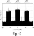
- Fig. 19 is a diagram showing a spectrum example of reception signals in a digital domain obtained by the signal detection device 10 of the first embodiment.
- the horizontal axis represents frequency (GHz), and the vertical axis represents intensity (10 dB/div).
- signals of a mode 3 (LP11b) (g301), a mode 1 (LP01) (g302), and a mode 2 (LP11a) (g303) are frequency-multiplexed every 12 (GHz) from the low frequency side.
- the signal processing unit 65 performed frequency shift by digital signal processing on signals of the mode 2 and the mode 3 of the present signals to convert the signals into baseband signals, and then demodulated original three QPSK signal sequences by MIMO equalization processing.
- Fig. 20 is a diagram showing constellation examples of QPSK obtained according to the first embodiment. As shown in Fig. 20 , in the evaluation, it can be confirmed that the signals of the three modes are received with high quality by the single reception unit 6 in the signal detection device 10 of the first embodiment.
- the signal detection device 10 (or 10A, 10B, 10C, 10D, 10E, 10F) of each of the embodiments includes the mode demultiplexer 3 that converts N spatial mode signals including a plurality of higher modes excited in the transmission path fiber 2 into N base modes and outputs the N basis modes, the space-frequency conversion unit 4 (or 4B, 4C, 4D, 4E, 4F) (frequency conversion unit) that converts the frequencies of respective optical signals, the N ⁇ 1 optical coupler 5 (combiner) that multiplexes N optical signals, and the reception unit 6 (or 6A) that photoelectrically converts a multiplexed optical signal while maintaining modulation information for a phase and polarization, performs digital signal conversion and signal processing, and demodulates an original information sequence.
- the mode demultiplexer 3 that converts N spatial mode signals including a plurality of higher modes excited in the transmission path fiber 2 into N base modes and outputs the N basis modes
- the space-frequency conversion unit 4 (or 4B, 4C, 4D, 4E
- a signal of a plurality of modes can be received by a reception unit of which the number is smaller than the number of the modes, so that the configuration in the reception device is reduced, the device size and power consumption can be reduced, and the manufacturing cost can be reduced.
- an optical transceiving module having characteristics of small size, low cost, and low power consumption and an optical transceiver using the same have been implemented by the digital coherent transmission technology without using a complicated phase locked loop or the like.
- the digital coherent transmission technology not only the reception sensitivity at the time of optical transmission forming a large-capacity optical network can be improved, but also the information transmission efficiency can be dramatically improved by information being superimposed on the amplitude, phase, or polarization of an optical carrier wave.
- the configuration in the reception device can be reduced.
- the signal detection device 10 may include a functional unit other than the above-described configuration.
- a signal input to the signal detection device 10 may be, for example, binary phase shift keying (BPSK), differential phase shift keying (DPSK), or the like.
- BPSK binary phase shift keying
- DPSK differential phase shift keying
- the present invention is applicable to a transmission system.
Landscapes
- Engineering & Computer Science (AREA)
- Computer Networks & Wireless Communication (AREA)
- Signal Processing (AREA)
- Physics & Mathematics (AREA)
- Electromagnetism (AREA)
- Optical Communication System (AREA)
Applications Claiming Priority (1)
| Application Number | Priority Date | Filing Date | Title |
|---|---|---|---|
| PCT/JP2021/034116 WO2023042340A1 (ja) | 2021-09-16 | 2021-09-16 | 信号検出装置、信号検出方法、およびプログラム |
Publications (2)
| Publication Number | Publication Date |
|---|---|
| EP4404481A1 true EP4404481A1 (de) | 2024-07-24 |
| EP4404481A4 EP4404481A4 (de) | 2025-07-30 |
Family
ID=85602599
Family Applications (1)
| Application Number | Title | Priority Date | Filing Date |
|---|---|---|---|
| EP21957521.4A Pending EP4404481A4 (de) | 2021-09-16 | 2021-09-16 | Signaldetektionsvorrichtung, signaldetektionsverfahren und programm |
Country Status (4)
| Country | Link |
|---|---|
| US (1) | US20240388376A1 (de) |
| EP (1) | EP4404481A4 (de) |
| JP (1) | JP7636698B2 (de) |
| WO (1) | WO2023042340A1 (de) |
Families Citing this family (1)
| Publication number | Priority date | Publication date | Assignee | Title |
|---|---|---|---|---|
| US11658461B1 (en) * | 2022-03-29 | 2023-05-23 | Quantum Valley Ideas Laboratories | Tuning the output of a laser |
Family Cites Families (10)
| Publication number | Priority date | Publication date | Assignee | Title |
|---|---|---|---|---|
| US9100085B2 (en) * | 2011-09-21 | 2015-08-04 | Spatial Digital Systems, Inc. | High speed multi-mode fiber transmissions via orthogonal wavefronts |
| JP5702697B2 (ja) | 2011-10-04 | 2015-04-15 | 日本電信電話株式会社 | モード多重伝送システム及びモード多重伝送方法 |
| US20140248052A1 (en) * | 2013-03-04 | 2014-09-04 | University Of Central Florida Research Foundation, Inc. | Mode-routed optical networks |
| JP6363979B2 (ja) | 2015-08-06 | 2018-07-25 | 日本電信電話株式会社 | デジタルコヒーレント受信機 |
| JP6378654B2 (ja) * | 2015-08-21 | 2018-08-22 | 日本電信電話株式会社 | 空間多重光伝送システム及び空間多重光伝送方法 |
| US10536238B2 (en) | 2016-01-12 | 2020-01-14 | Nippon Telegraph And Telephone Corporation | Optical transmission system, optical transmission apparatus, and optical reception apparatus |
| WO2017145901A1 (ja) | 2016-02-25 | 2017-08-31 | Kddi株式会社 | 光通信システム、光送信装置及び光受信装置 |
| JP6529925B2 (ja) * | 2016-04-12 | 2019-06-12 | 日本電信電話株式会社 | モード合分波器、光伝送システム及び中継伝送システム |
| JP7352118B2 (ja) | 2020-02-19 | 2023-09-28 | 日本電信電話株式会社 | 光伝送システム及び光伝送方法 |
| CN113315577B (zh) * | 2021-05-18 | 2022-11-01 | 广东工业大学 | 一种少模全光放大方法、系统和少模光纤通信系统 |
-
2021
- 2021-09-16 WO PCT/JP2021/034116 patent/WO2023042340A1/ja not_active Ceased
- 2021-09-16 EP EP21957521.4A patent/EP4404481A4/de active Pending
- 2021-09-16 US US18/691,536 patent/US20240388376A1/en active Pending
- 2021-09-16 JP JP2023548030A patent/JP7636698B2/ja active Active
Also Published As
| Publication number | Publication date |
|---|---|
| JPWO2023042340A1 (de) | 2023-03-23 |
| EP4404481A4 (de) | 2025-07-30 |
| US20240388376A1 (en) | 2024-11-21 |
| WO2023042340A1 (ja) | 2023-03-23 |
| JP7636698B2 (ja) | 2025-02-27 |
Similar Documents
| Publication | Publication Date | Title |
|---|---|---|
| US11652553B2 (en) | Optical signal transmission system and optical signal transmission method | |
| KR101402641B1 (ko) | 멀티―캐리어 광 신호의 디지털 코히어런트 검출 | |
| JP5034770B2 (ja) | コヒーレント光受信器および光通信システム | |
| Yu et al. | A novel scheme to generate single-sideband millimeter-wave signals by using low-frequency local oscillator signal | |
| CN101729187B (zh) | 一种光信号传输处理方法、发送装置及系统 | |
| JPH11331089A (ja) | 光伝送システムならびにそれに用いられる光送信装置および光受信装置 | |
| CN105099570A (zh) | 正交多载波光源及pdm-qpsk信号发射装置 | |
| US11888528B2 (en) | Optical communication system | |
| CN116996128B (zh) | 光纤传输系统及装置 | |
| US20210384976A1 (en) | Communication system for radio transmission | |
| Browning et al. | Phase noise robust optical heterodyne system for reduced complexity millimeter-wave analog radio-over-fibre | |
| Xu et al. | Demonstration of 60 Gb/s W-band optical mm-wave signal full-duplex transmission over fiber-wireless-fiber network | |
| WO2018198873A1 (ja) | 光伝送方法および光伝送装置 | |
| Zhou et al. | Photonic generation of frequency quadrupling signal for millimeter-wave communication | |
| US9106354B2 (en) | Optical frequency-division multiplexer, optical communication system, and optical frequency-division multiplexing method | |
| JP7759056B2 (ja) | 光無線通信システム、信号処理装置、無線通信装置、光無線通信方法、信号処理方法及び無線通信方法 | |
| EP4404481A1 (de) | Signaldetektionsvorrichtung, signaldetektionsverfahren und programm | |
| Watanabe et al. | All-optical data frequency multiplexing on single-wavelength carrier light by sequentially provided cross-phase modulation in fiber | |
| Chang et al. | Architectures and enabling technologies for super-broadband radio-over-fiber optical-wireless access networks | |
| Tan et al. | Wavelength translation of dual-polarization phase-modulated Nyquist OTDM at terabit/s | |
| Zeng et al. | Photonic aggregation of microwave signals with electro-optic modulation and polarization combination | |
| Xu et al. | Demonstration of 120 Gbit/s full-duplex signal transmission over fiber-wireless-fiber network at W-band | |
| Huang et al. | Spectrum-efficient uplink transmission for mobile fronthaul based on coherent detection | |
| Elschner et al. | Distributed aggregation of spectrally efficient single-and dual-polarization super-channels by optical frequency conversion in fiber | |
| Othman et al. | Integrated Comb Laser With Active De-Multiplexer for Spectrally Sliced Coherent Receiver |
Legal Events
| Date | Code | Title | Description |
|---|---|---|---|
| STAA | Information on the status of an ep patent application or granted ep patent |
Free format text: STATUS: THE INTERNATIONAL PUBLICATION HAS BEEN MADE |
|
| PUAI | Public reference made under article 153(3) epc to a published international application that has entered the european phase |
Free format text: ORIGINAL CODE: 0009012 |
|
| STAA | Information on the status of an ep patent application or granted ep patent |
Free format text: STATUS: REQUEST FOR EXAMINATION WAS MADE |
|
| 17P | Request for examination filed |
Effective date: 20240313 |
|
| AK | Designated contracting states |
Kind code of ref document: A1 Designated state(s): AL AT BE BG CH CY CZ DE DK EE ES FI FR GB GR HR HU IE IS IT LI LT LU LV MC MK MT NL NO PL PT RO RS SE SI SK SM TR |
|
| DAV | Request for validation of the european patent (deleted) | ||
| DAX | Request for extension of the european patent (deleted) | ||
| A4 | Supplementary search report drawn up and despatched |
Effective date: 20250701 |
|
| RIC1 | Information provided on ipc code assigned before grant |
Ipc: H04B 10/2581 20130101AFI20250625BHEP Ipc: H04B 10/60 20130101ALI20250625BHEP Ipc: H04J 14/04 20060101ALI20250625BHEP |
|
| RAP3 | Party data changed (applicant data changed or rights of an application transferred) |
Owner name: NTT, INC. |
|
| GRAP | Despatch of communication of intention to grant a patent |
Free format text: ORIGINAL CODE: EPIDOSNIGR1 |
|
| STAA | Information on the status of an ep patent application or granted ep patent |
Free format text: STATUS: GRANT OF PATENT IS INTENDED |
|
| INTG | Intention to grant announced |
Effective date: 20260304 |