EP4398317A1 - Verfahren zur herstellung eines wachstumssubstrats mit mesas mit unterschiedlicher verformbarkeit durch elektrochemisches ätzen und porösmachung - Google Patents
Verfahren zur herstellung eines wachstumssubstrats mit mesas mit unterschiedlicher verformbarkeit durch elektrochemisches ätzen und porösmachung Download PDFInfo
- Publication number
- EP4398317A1 EP4398317A1 EP23218208.9A EP23218208A EP4398317A1 EP 4398317 A1 EP4398317 A1 EP 4398317A1 EP 23218208 A EP23218208 A EP 23218208A EP 4398317 A1 EP4398317 A1 EP 4398317A1
- Authority
- EP
- European Patent Office
- Prior art keywords
- mesas
- layer
- epitaxy
- growth substrate
- ingan
- Prior art date
- Legal status (The legal status is an assumption and is not a legal conclusion. Google has not performed a legal analysis and makes no representation as to the accuracy of the status listed.)
- Pending
Links
Images



Classifications
-
- H—ELECTRICITY
- H10—SEMICONDUCTOR DEVICES; ELECTRIC SOLID-STATE DEVICES NOT OTHERWISE PROVIDED FOR
- H10H—INORGANIC LIGHT-EMITTING SEMICONDUCTOR DEVICES HAVING POTENTIAL BARRIERS
- H10H20/00—Individual inorganic light-emitting semiconductor devices having potential barriers, e.g. light-emitting diodes [LED]
- H10H20/01—Manufacture or treatment
- H10H20/011—Manufacture or treatment of bodies, e.g. forming semiconductor layers
- H10H20/013—Manufacture or treatment of bodies, e.g. forming semiconductor layers having light-emitting regions comprising only Group III-V materials
- H10H20/0137—Manufacture or treatment of bodies, e.g. forming semiconductor layers having light-emitting regions comprising only Group III-V materials the light-emitting regions comprising nitride materials
-
- H—ELECTRICITY
- H10—SEMICONDUCTOR DEVICES; ELECTRIC SOLID-STATE DEVICES NOT OTHERWISE PROVIDED FOR
- H10F—INORGANIC SEMICONDUCTOR DEVICES SENSITIVE TO INFRARED RADIATION, LIGHT, ELECTROMAGNETIC RADIATION OF SHORTER WAVELENGTH OR CORPUSCULAR RADIATION
- H10F39/00—Integrated devices, or assemblies of multiple devices, comprising at least one element covered by group H10F30/00, e.g. radiation detectors comprising photodiode arrays
- H10F39/011—Manufacture or treatment of image sensors covered by group H10F39/12
- H10F39/026—Wafer-level processing
-
- H—ELECTRICITY
- H10—SEMICONDUCTOR DEVICES; ELECTRIC SOLID-STATE DEVICES NOT OTHERWISE PROVIDED FOR
- H10H—INORGANIC LIGHT-EMITTING SEMICONDUCTOR DEVICES HAVING POTENTIAL BARRIERS
- H10H20/00—Individual inorganic light-emitting semiconductor devices having potential barriers, e.g. light-emitting diodes [LED]
- H10H20/80—Constructional details
- H10H20/81—Bodies
- H10H20/819—Bodies characterised by their shape, e.g. curved or truncated substrates
-
- H—ELECTRICITY
- H10—SEMICONDUCTOR DEVICES; ELECTRIC SOLID-STATE DEVICES NOT OTHERWISE PROVIDED FOR
- H10H—INORGANIC LIGHT-EMITTING SEMICONDUCTOR DEVICES HAVING POTENTIAL BARRIERS
- H10H20/00—Individual inorganic light-emitting semiconductor devices having potential barriers, e.g. light-emitting diodes [LED]
- H10H20/80—Constructional details
- H10H20/81—Bodies
- H10H20/822—Materials of the light-emitting regions
- H10H20/824—Materials of the light-emitting regions comprising only Group III-V materials, e.g. GaP
- H10H20/825—Materials of the light-emitting regions comprising only Group III-V materials, e.g. GaP containing nitrogen, e.g. GaN
-
- H—ELECTRICITY
- H10—SEMICONDUCTOR DEVICES; ELECTRIC SOLID-STATE DEVICES NOT OTHERWISE PROVIDED FOR
- H10H—INORGANIC LIGHT-EMITTING SEMICONDUCTOR DEVICES HAVING POTENTIAL BARRIERS
- H10H29/00—Integrated devices, or assemblies of multiple devices, comprising at least one light-emitting semiconductor element covered by group H10H20/00
- H10H29/10—Integrated devices comprising at least one light-emitting semiconductor component covered by group H10H20/00
- H10H29/14—Integrated devices comprising at least one light-emitting semiconductor component covered by group H10H20/00 comprising multiple light-emitting semiconductor components
-
- H—ELECTRICITY
- H10—SEMICONDUCTOR DEVICES; ELECTRIC SOLID-STATE DEVICES NOT OTHERWISE PROVIDED FOR
- H10H—INORGANIC LIGHT-EMITTING SEMICONDUCTOR DEVICES HAVING POTENTIAL BARRIERS
- H10H29/00—Integrated devices, or assemblies of multiple devices, comprising at least one light-emitting semiconductor element covered by group H10H20/00
- H10H29/10—Integrated devices comprising at least one light-emitting semiconductor component covered by group H10H20/00
- H10H29/14—Integrated devices comprising at least one light-emitting semiconductor component covered by group H10H20/00 comprising multiple light-emitting semiconductor components
- H10H29/142—Two-dimensional arrangements, e.g. asymmetric LED layout
-
- H—ELECTRICITY
- H10—SEMICONDUCTOR DEVICES; ELECTRIC SOLID-STATE DEVICES NOT OTHERWISE PROVIDED FOR
- H10P—GENERIC PROCESSES OR APPARATUS FOR THE MANUFACTURE OR TREATMENT OF DEVICES COVERED BY CLASS H10
- H10P50/00—Etching of wafers, substrates or parts of devices
-
- H—ELECTRICITY
- H10—SEMICONDUCTOR DEVICES; ELECTRIC SOLID-STATE DEVICES NOT OTHERWISE PROVIDED FOR
- H10P—GENERIC PROCESSES OR APPARATUS FOR THE MANUFACTURE OR TREATMENT OF DEVICES COVERED BY CLASS H10
- H10P50/00—Etching of wafers, substrates or parts of devices
- H10P50/60—Wet etching
- H10P50/61—Electrolytic etching
- H10P50/617—Electrolytic etching of Group III-V materials
-
- H—ELECTRICITY
- H10—SEMICONDUCTOR DEVICES; ELECTRIC SOLID-STATE DEVICES NOT OTHERWISE PROVIDED FOR
- H10H—INORGANIC LIGHT-EMITTING SEMICONDUCTOR DEVICES HAVING POTENTIAL BARRIERS
- H10H20/00—Individual inorganic light-emitting semiconductor devices having potential barriers, e.g. light-emitting diodes [LED]
- H10H20/80—Constructional details
- H10H20/81—Bodies
- H10H20/815—Bodies having stress relaxation structures, e.g. buffer layers
-
- H—ELECTRICITY
- H10—SEMICONDUCTOR DEVICES; ELECTRIC SOLID-STATE DEVICES NOT OTHERWISE PROVIDED FOR
- H10P—GENERIC PROCESSES OR APPARATUS FOR THE MANUFACTURE OR TREATMENT OF DEVICES COVERED BY CLASS H10
- H10P50/00—Etching of wafers, substrates or parts of devices
- H10P50/20—Dry etching; Plasma etching; Reactive-ion etching
- H10P50/24—Dry etching; Plasma etching; Reactive-ion etching of semiconductor materials
- H10P50/242—Dry etching; Plasma etching; Reactive-ion etching of semiconductor materials of Group IV materials
-
- H—ELECTRICITY
- H10—SEMICONDUCTOR DEVICES; ELECTRIC SOLID-STATE DEVICES NOT OTHERWISE PROVIDED FOR
- H10P—GENERIC PROCESSES OR APPARATUS FOR THE MANUFACTURE OR TREATMENT OF DEVICES COVERED BY CLASS H10
- H10P50/00—Etching of wafers, substrates or parts of devices
- H10P50/60—Wet etching
- H10P50/64—Wet etching of semiconductor materials
- H10P50/642—Chemical etching
- H10P50/646—Chemical etching of Group III-V materials
Definitions
- the diode matrix can then include diodes adapted to emit red light, other diodes green light, and still others blue light. Such a matrix of diodes then forms a micro-screen with native RGB emission (for Red, Green, Blue, in English).
- the diodes are said to have native emission, in the sense that the active zone of each diode emitting at a given wavelength differs from the active zones of the diodes emitting at another wavelength.
- the active zones differ from each other by the proportion of indium in the quantum wells.
- Such a matrix of native emission diodes is thus distinguished from color conversion technologies where the diodes all emit at the same wavelength, for example in blue, and are each coated with a pad comprising phosphors, for example semiconductor nanocrystals forming quantum dots, to convert at least part of the incident light into light of another wavelength.
- the document EP3840065A1 describes an example of a process for manufacturing a growth substrate then a diode matrix using the electrochemical porosification technique.
- the method comprises the production of a growth substrate (also called pseudo-substrate) having several InGaN mesas, each formed of a portion doped with rendered InGaN porous during an electrochemical porosification step, and an epitaxy recovery portion in InGaN not intentionally doped or lightly doped so that it is not porosified (it remains intact or dense, therefore not porous).
- the diodes are then produced by epitaxy from the epitaxy recovery portions.
- the doped portions of the mesas can have different doping levels from one mesa to another, so that the mesas have different porosification levels and therefore different relaxation rates.
- the diodes made from the different mesas then include quantum wells having a more or less significant proportion of indium, thus making it possible to obtain emissive pixels at different wavelengths.
- the invention aims to remedy at least in part the drawbacks of the prior art, and more particularly to propose a method of manufacturing a growth substrate, suitable for producing a matrix of diodes based on InGaN, and comprising mesas of different deformabilities, without it being necessary to carry out spatially localized implantations of dopants.
- These mesas of different deformabilities thus make it possible to natively produce InGaN-based diodes that can each emit or detect light radiation at different wavelengths, for example in the three RGB colors.
- the removal step can be carried out by photoelectrochemical etching of the intermediate separation portion of at least the M3 mesas, the M1 mesas being covered by an encapsulation layer.
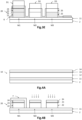
- the removal step can be carried out by dry etching of the upper portion of at least the mesas M3, with stopping of etching on the intermediate separation portion, the mesas M1 being covered by an etching mask.
- the intermediate separation portion can be, in each mesa, on and in contact with the lower portion, the method then comprising a step of producing portions of epitaxy recovery carried out at InGaN base, carried out after the electrochemical porosification step, resting on the upper portion in the M1 mesas, and resting on the lower portion in the M3 mesas.
- an epitaxy recovery layer can be located on and in contact with the lower layer, so that, following the removal and porosification steps, the M3 mesas have an upper face formed by an epitaxy recovery portion originating from the epitaxy recovery layer.
- the invention also relates to a method for manufacturing a matrix of diodes of categories D1, D2, D3 from a growth substrate, comprising the following steps: manufacturing the growth substrate by the method according to any one previous characteristics; then deposition of a growth mask, leaving an upper surface of the mesas M1, M2, M3 free; then production of the diode matrix D1, D2, D3, respectively from the mesas M1, M2, M3.
- Each mesa M1, M2, M3 may include a non-porous sealing portion made from GaN, located, in the mesas M1, between and in contact with the upper portion and the epitaxy recovery portion, and in the mesas M3, between and in contact with the lower portion and the epitaxy recovery portion.
- the intermediate epitaxy recovery portion can be porous in the M1 mesas, and non-porous in the M2 and M3 mesas.
- the growth substrate is suitable for the production by epitaxy of a matrix of diodes based on InGaN, the diodes making it possible to emit or detect, in a native manner, light radiation at different wavelengths, for example of RGB type (red, green, blue).
- RGB type red, green, blue
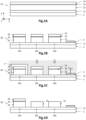
- the manufacturing process proposes to first produce mesas M1, M2, M3 based on GaN, each comprising a lower portion based on GaN, an intermediate portion called separation portion based on InGaN, and a portion higher than AlGaN base. Then, the upper AIGaN-based portion of at least the M3 mesas, and possibly the M2 mesas as well, are removed by etching, while they are preserved in the M1 mesas.
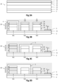
- This removal step can be, in a first embodiment, carried out by photoelectrochemical etching of the intermediate separation portion based on InGaN, or, in a second embodiment, carried out by dry etching of the upper portions based on AlGaN with etching stop on the separation intermediate portions based on InGaN.
- the process also provides for porosification by electrochemical porosification of the lower portions of the mesas M1 and M3 only, whereas they are not porosified in the mesas M2.
- the support substrate 2 is made here of a non-porosifiable material, so that it remains non-porous (dense) during the subsequent porosification of the mesas M1 and M3. It may be a material inert to the electrochemical porosification reaction, such as an insulating material (sapphire, etc.) or a semiconductor material (SiC, Si, etc.) not intentionally doped (nest) or weakly doped. . It may also be a semiconductor material based on GaN that is not intentionally doped or weakly doped so as not to be porosifiable at the porosification voltage V ECE .
- the support layer can be made of sapphire, silicon, SiC, freestanding GaN, among others.
- the support substrate 2 may be absent if the conductive buffer layer 11 has a sufficient thickness to ensure the mechanical strength of the growth substrate 20.
- it is made of n-type doped GaN with a doping level of approximately 6 ⁇ 10 18 cm -3 .
- Its thickness is of the order of several hundred nanometers to allow good relaxation of the mechanical constraints of the mesas M1 and M3, for example at least equal to 500nm, and is here equal to approximately 1000nm.
- the separation interlayer 13 rests on the lower layer 12, and is here in contact with it. It is intended to be etched, during the subsequent photoelectrochemical etching step, to ensure the removal of the upper portions 24 of only the mesas M2 and M3 (and not the mesas M1). It is therefore a sacrificial layer. It is made from In x Ga 1-x N, with a non-zero proportion of indium x greater than those of the lower 12 and upper 14 layers, for example between 10 and 15%, to be the only one to absorb the excitation light beam during the subsequent photoelectrochemical etching step. In other words, its bandgap energy is lower than that of the lower 12 and upper 14 layers.
- In this example it is made of non-intentionally doped InGaN, with a proportion of indium x of approximately 15%. Its thickness is of the order of a few nanometers, for example approximately 3nm. It can thus form a single quantum well or several quantum wells. Note that InGaN porosifies at an electrical voltage V ECE lower than that of GaN, at an equivalent doping level. The proportion of indium x and the doping level are chosen here so that the intermediate separation portion 23 is not porosified during the porosification step of the fig.1E .
- the upper layer 14 rests on the separation interlayer 13, and is here in contact with it. It is intended to form the upper portions 24 of the mesas, of which that of the M3 mesas will be deleted (and here also that of the M2 mesas) during the subsequent photoelectrochemical etching step, and that of the M1 mesas will be retained. It is made from Al y Ga 1-y N, with a non-zero proportion of aluminum y, greater than those of the lower layers 12 and interlayer 13. The doping level is chosen so that the upper portion 24 of the mesas M1 is not porosified during the subsequent electrochemical porosification step. The material can therefore be unintentionally doped or weakly doped.
- the mesas M1, M2 and M3 are produced by structuring the crystalline stack 10 by lithography and localized etching.
- the etching is carried out here until it emerges on the upper face of the conductive buffer layer 11.
- the etching can be a dry etching, for example of the ICP-RIE plasma type with chlorine gas, so that the sides of the mesas are substantially vertical .
- Each mesa is formed of a stack, in the +Z direction, of a lower portion 22 based on GaN (from the lower layer 12), an intermediate separation portion 23 based on InGaN (from the interlayer 13), and an upper portion 24 based on AlGaN (from the upper layer 14).
- each portion of a mesa is coplanar with the corresponding portions of the other mesas and has the same thickness.
- a polarization electrode 3 is then deposited on and in contact with the conductive buffer layer 11, which will make it possible to apply an electric potential to the mesas.
- the encapsulation layer 4 is first deposited on the mesas M1, so as to cover them completely.
- the mesas M2 and M3 are not covered by this layer 4. It can be a photosensitive resin, or even a conformal layer of an oxide.
- the intermediate portion 23 of the mesas M1 will therefore not be in contact with the liquid electrolyte.
- the encapsulation layer 4 is removed.
- the mesas M2 and M3 have therefore lost their upper portion 24, due to the total etching of the intermediate portions 23.
- the upper face therefore corresponds to that of the lower portions 22.
- the upper face of the mesas M1 always corresponds to the upper portion 24 (or to the thin protective portion).
- the separation intermediate layer 13 provides a function of stopping etching during the step of removing the upper portions 24 of at least the mesas M3 (and here also the mesas M2) . It is made from InGaN with a sufficient proportion of indium to ensure etching selectivity at the AIGaN/InGaN interface.
- the mesas M1, M2 and M3 are then produced during a first dry etching step, for example by RIE etching with a first etching agent.
- the etching agent is chosen to be able to locally etch the upper layer 14 based on AIGaN, then the interlayer 13 based on InGaN, and finally the lower layer 12 based on GaN.
- the engraving mask can be arranged here to protect the top of the mesas.
Landscapes
- Led Devices (AREA)
- Crystals, And After-Treatments Of Crystals (AREA)
Applications Claiming Priority (1)
| Application Number | Priority Date | Filing Date | Title |
|---|---|---|---|
| FR2214167A FR3144485B1 (fr) | 2022-12-21 | 2022-12-21 | Procédé de fabrication d’un substrat de croissance comportant des mésas de différentes deformabilites, par gravure et porosification électrochimique |
Publications (1)
| Publication Number | Publication Date |
|---|---|
| EP4398317A1 true EP4398317A1 (de) | 2024-07-10 |
Family
ID=85685553
Family Applications (1)
| Application Number | Title | Priority Date | Filing Date |
|---|---|---|---|
| EP23218208.9A Pending EP4398317A1 (de) | 2022-12-21 | 2023-12-19 | Verfahren zur herstellung eines wachstumssubstrats mit mesas mit unterschiedlicher verformbarkeit durch elektrochemisches ätzen und porösmachung |
Country Status (4)
| Country | Link |
|---|---|
| US (1) | US20240213398A1 (de) |
| EP (1) | EP4398317A1 (de) |
| CN (1) | CN118231532A (de) |
| FR (1) | FR3144485B1 (de) |
Citations (4)
| Publication number | Priority date | Publication date | Assignee | Title |
|---|---|---|---|---|
| EP3840016A1 (de) | 2019-12-19 | 2021-06-23 | Commissariat à l'énergie atomique et aux énergies alternatives | Verfahren zur herstellung eines substrats, das eine entspannte ingan-schicht umfasst |
| EP3840065A1 (de) | 2019-12-19 | 2021-06-23 | Commissariat à l'énergie atomique et aux énergies alternatives | Verfahren zur herstellung einer entspannten gan/ingan-struktur |
| US20220285584A1 (en) * | 2021-03-08 | 2022-09-08 | Applied Materials, Inc. | Indium-gallium-nitride light emitting diodes with light reflecting mirrors |
| CN115483321A (zh) * | 2021-06-16 | 2022-12-16 | 法国原子能源和替代能源委员会 | 用于制造自然发射矩阵的方法 |
Family Cites Families (6)
| Publication number | Priority date | Publication date | Assignee | Title |
|---|---|---|---|---|
| FR3099966B1 (fr) * | 2019-08-16 | 2021-09-24 | Commissariat Energie Atomique | Procédé de fabrication de dispositifs optoélectroniques |
| TW202211498A (zh) * | 2020-08-04 | 2022-03-16 | 英商普羅科技有限公司 | Led裝置及製造方法 |
| DE102020128679A1 (de) * | 2020-10-30 | 2022-05-05 | OSRAM Opto Semiconductors Gesellschaft mit beschränkter Haftung | Optoelektronisches bauelement und verfahren zur herstellung eines halbleiterkörpers |
| US20220208848A1 (en) * | 2020-12-30 | 2022-06-30 | Facebook Technologies, Llc | Engineered wafer with selective porosification for multi-color light emission |
| US12336326B2 (en) * | 2022-06-12 | 2025-06-17 | Mikro Mesa Technology Co., Ltd. | Method of manufacturing micro devices |
| FR3141558B1 (fr) * | 2022-10-28 | 2025-12-05 | Commissariat Energie Atomique | Substrat de croissance de matrice de diodes, comportant des mésas présentant différents niveaux de porosification |
-
2022
- 2022-12-21 FR FR2214167A patent/FR3144485B1/fr active Active
-
2023
- 2023-12-19 US US18/545,026 patent/US20240213398A1/en active Pending
- 2023-12-19 EP EP23218208.9A patent/EP4398317A1/de active Pending
- 2023-12-21 CN CN202311768150.2A patent/CN118231532A/zh active Pending
Patent Citations (5)
| Publication number | Priority date | Publication date | Assignee | Title |
|---|---|---|---|---|
| EP3840016A1 (de) | 2019-12-19 | 2021-06-23 | Commissariat à l'énergie atomique et aux énergies alternatives | Verfahren zur herstellung eines substrats, das eine entspannte ingan-schicht umfasst |
| EP3840065A1 (de) | 2019-12-19 | 2021-06-23 | Commissariat à l'énergie atomique et aux énergies alternatives | Verfahren zur herstellung einer entspannten gan/ingan-struktur |
| US20220285584A1 (en) * | 2021-03-08 | 2022-09-08 | Applied Materials, Inc. | Indium-gallium-nitride light emitting diodes with light reflecting mirrors |
| CN115483321A (zh) * | 2021-06-16 | 2022-12-16 | 法国原子能源和替代能源委员会 | 用于制造自然发射矩阵的方法 |
| FR3124313A1 (fr) * | 2021-06-16 | 2022-12-23 | Commissariat A L'energie Atomique Et Aux Energies Alternatives | Procede de fabrication d’une matrice a emission native |
Non-Patent Citations (1)
| Title |
|---|
| GRIFFINOLIVER: "Porous nitride semiconductors reviewed,", J. PHYS. D: APPL. PHYS., vol. 53, 2020, pages 383002 |
Also Published As
| Publication number | Publication date |
|---|---|
| US20240213398A1 (en) | 2024-06-27 |
| CN118231532A (zh) | 2024-06-21 |
| FR3144485B1 (fr) | 2024-12-13 |
| FR3144485A1 (fr) | 2024-06-28 |
Similar Documents
| Publication | Publication Date | Title |
|---|---|---|
| EP3840016A1 (de) | Verfahren zur herstellung eines substrats, das eine entspannte ingan-schicht umfasst | |
| EP3503222B1 (de) | Verfahren zur herstellung einer optoelektronischen vorrichtung durch aufbringen einer konvertierungsstruktur auf eine emissionsstruktur | |
| EP4418308A2 (de) | Verfahren zur herstellung einer relaxierten gan/ingan-struktur | |
| FR2967813A1 (fr) | Procédé de réalisation d'une structure a couche métallique enterrée | |
| EP4105999B1 (de) | Verfahren zur herstellung einer nativen emissionsmatrix | |
| EP4379800B1 (de) | Verfahren zur herstellung eines wachstumssubstrats mit unterschiedlichen elektrochemische porosifikationsebenen mit mesas mit unterschiedlichen porenbildungsgraden | |
| FR3026558A1 (fr) | Procede d'activation de dopants dans une couche semi-conductrice a base de gan | |
| EP4362101B1 (de) | Diodenmatrixwachstumssubstrat mit mesas mit verschiedenen porenbildungsebenen | |
| EP4383359A1 (de) | Verfahren zur porenbildung von mesa aus (al,in,ga)n/(al,in,ga)n und entsprechende struktur | |
| EP3563426B1 (de) | Verfahren zur herstellung einer optoelektronischen vorrichtung mit einem schritt zum ätzen der rückseite des wachstumssubstrats | |
| FR3143850A1 (fr) | Procédé de réalisation d’un dispositif électronique | |
| EP3853882B1 (de) | Verfahren zur herstellung einer elektronischen vorrichtung | |
| EP4521891A1 (de) | Verfahren zur porenbildung von mesa (al,in,ga)n/(al,in,ga)n | |
| WO2014154993A1 (fr) | Procédé de fabrication d'une structure à multijonctions pour cellule photovoltaïque | |
| FR3144485A1 (fr) | Procédé de fabrication d’un substrat de croissance comportant des mésas de différentes deformabilites, par gravure et porosification électrochimique | |
| EP4639638A1 (de) | Verfahren zur herstellung einer mesastruktur zur herstellung eines kontaktes | |
| EP4102579A1 (de) | Verfahren zur herstellung eines substrats mit einer relaxierten inganschicht und so erhaltenes substrat für die wiederaufnahme des wachstums einer led-struktur | |
| EP3903341B1 (de) | Verfahren zur herstellung eines substrats für einen vorderseitigen bildsensor | |
| EP4679983A1 (de) | Verfahren zur herstellung einer photonischen vorrichtung und entsprechende photonische vorrichtung | |
| EP4391064B1 (de) | Verfahren zur herstellung von mikro-leds und resultierende struktur mit mikro-leds | |
| FR3154229A1 (fr) | Procédé de croissance d’un matériau III-N | |
| WO2024141738A1 (fr) | Procédé de fabrication d'un capteur d'image |
Legal Events
| Date | Code | Title | Description |
|---|---|---|---|
| PUAI | Public reference made under article 153(3) epc to a published international application that has entered the european phase |
Free format text: ORIGINAL CODE: 0009012 |
|
| STAA | Information on the status of an ep patent application or granted ep patent |
Free format text: STATUS: REQUEST FOR EXAMINATION WAS MADE |
|
| 17P | Request for examination filed |
Effective date: 20231219 |
|
| AK | Designated contracting states |
Kind code of ref document: A1 Designated state(s): AL AT BE BG CH CY CZ DE DK EE ES FI FR GB GR HR HU IE IS IT LI LT LU LV MC ME MK MT NL NO PL PT RO RS SE SI SK SM TR |
|
| RAP3 | Party data changed (applicant data changed or rights of an application transferred) |
Owner name: COMMISSARIAT A L'ENERGIE ATOMIQUE ET AUX ENERGIESALTERNATIVES |