EP4398317A1 - Process for manufacturing a growth substrate comprising mesas with different deformability, by electrochemical etching and porosification - Google Patents
Process for manufacturing a growth substrate comprising mesas with different deformability, by electrochemical etching and porosification Download PDFInfo
- Publication number
- EP4398317A1 EP4398317A1 EP23218208.9A EP23218208A EP4398317A1 EP 4398317 A1 EP4398317 A1 EP 4398317A1 EP 23218208 A EP23218208 A EP 23218208A EP 4398317 A1 EP4398317 A1 EP 4398317A1
- Authority
- EP
- European Patent Office
- Prior art keywords
- mesas
- layer
- epitaxy
- growth substrate
- ingan
- Prior art date
- Legal status (The legal status is an assumption and is not a legal conclusion. Google has not performed a legal analysis and makes no representation as to the accuracy of the status listed.)
- Pending
Links
Images



Classifications
-
- H—ELECTRICITY
- H10—SEMICONDUCTOR DEVICES; ELECTRIC SOLID-STATE DEVICES NOT OTHERWISE PROVIDED FOR
- H10H—INORGANIC LIGHT-EMITTING SEMICONDUCTOR DEVICES HAVING POTENTIAL BARRIERS
- H10H20/00—Individual inorganic light-emitting semiconductor devices having potential barriers, e.g. light-emitting diodes [LED]
- H10H20/01—Manufacture or treatment
- H10H20/011—Manufacture or treatment of bodies, e.g. forming semiconductor layers
- H10H20/013—Manufacture or treatment of bodies, e.g. forming semiconductor layers having light-emitting regions comprising only Group III-V materials
- H10H20/0137—Manufacture or treatment of bodies, e.g. forming semiconductor layers having light-emitting regions comprising only Group III-V materials the light-emitting regions comprising nitride materials
-
- H—ELECTRICITY
- H10—SEMICONDUCTOR DEVICES; ELECTRIC SOLID-STATE DEVICES NOT OTHERWISE PROVIDED FOR
- H10F—INORGANIC SEMICONDUCTOR DEVICES SENSITIVE TO INFRARED RADIATION, LIGHT, ELECTROMAGNETIC RADIATION OF SHORTER WAVELENGTH OR CORPUSCULAR RADIATION
- H10F39/00—Integrated devices, or assemblies of multiple devices, comprising at least one element covered by group H10F30/00, e.g. radiation detectors comprising photodiode arrays
- H10F39/011—Manufacture or treatment of image sensors covered by group H10F39/12
- H10F39/026—Wafer-level processing
-
- H—ELECTRICITY
- H10—SEMICONDUCTOR DEVICES; ELECTRIC SOLID-STATE DEVICES NOT OTHERWISE PROVIDED FOR
- H10H—INORGANIC LIGHT-EMITTING SEMICONDUCTOR DEVICES HAVING POTENTIAL BARRIERS
- H10H20/00—Individual inorganic light-emitting semiconductor devices having potential barriers, e.g. light-emitting diodes [LED]
- H10H20/80—Constructional details
- H10H20/81—Bodies
- H10H20/819—Bodies characterised by their shape, e.g. curved or truncated substrates
-
- H—ELECTRICITY
- H10—SEMICONDUCTOR DEVICES; ELECTRIC SOLID-STATE DEVICES NOT OTHERWISE PROVIDED FOR
- H10H—INORGANIC LIGHT-EMITTING SEMICONDUCTOR DEVICES HAVING POTENTIAL BARRIERS
- H10H20/00—Individual inorganic light-emitting semiconductor devices having potential barriers, e.g. light-emitting diodes [LED]
- H10H20/80—Constructional details
- H10H20/81—Bodies
- H10H20/822—Materials of the light-emitting regions
- H10H20/824—Materials of the light-emitting regions comprising only Group III-V materials, e.g. GaP
- H10H20/825—Materials of the light-emitting regions comprising only Group III-V materials, e.g. GaP containing nitrogen, e.g. GaN
-
- H—ELECTRICITY
- H10—SEMICONDUCTOR DEVICES; ELECTRIC SOLID-STATE DEVICES NOT OTHERWISE PROVIDED FOR
- H10H—INORGANIC LIGHT-EMITTING SEMICONDUCTOR DEVICES HAVING POTENTIAL BARRIERS
- H10H29/00—Integrated devices, or assemblies of multiple devices, comprising at least one light-emitting semiconductor element covered by group H10H20/00
- H10H29/10—Integrated devices comprising at least one light-emitting semiconductor component covered by group H10H20/00
- H10H29/14—Integrated devices comprising at least one light-emitting semiconductor component covered by group H10H20/00 comprising multiple light-emitting semiconductor components
-
- H—ELECTRICITY
- H10—SEMICONDUCTOR DEVICES; ELECTRIC SOLID-STATE DEVICES NOT OTHERWISE PROVIDED FOR
- H10H—INORGANIC LIGHT-EMITTING SEMICONDUCTOR DEVICES HAVING POTENTIAL BARRIERS
- H10H29/00—Integrated devices, or assemblies of multiple devices, comprising at least one light-emitting semiconductor element covered by group H10H20/00
- H10H29/10—Integrated devices comprising at least one light-emitting semiconductor component covered by group H10H20/00
- H10H29/14—Integrated devices comprising at least one light-emitting semiconductor component covered by group H10H20/00 comprising multiple light-emitting semiconductor components
- H10H29/142—Two-dimensional arrangements, e.g. asymmetric LED layout
-
- H—ELECTRICITY
- H10—SEMICONDUCTOR DEVICES; ELECTRIC SOLID-STATE DEVICES NOT OTHERWISE PROVIDED FOR
- H10P—GENERIC PROCESSES OR APPARATUS FOR THE MANUFACTURE OR TREATMENT OF DEVICES COVERED BY CLASS H10
- H10P50/00—Etching of wafers, substrates or parts of devices
-
- H—ELECTRICITY
- H10—SEMICONDUCTOR DEVICES; ELECTRIC SOLID-STATE DEVICES NOT OTHERWISE PROVIDED FOR
- H10P—GENERIC PROCESSES OR APPARATUS FOR THE MANUFACTURE OR TREATMENT OF DEVICES COVERED BY CLASS H10
- H10P50/00—Etching of wafers, substrates or parts of devices
- H10P50/60—Wet etching
- H10P50/61—Electrolytic etching
- H10P50/617—Electrolytic etching of Group III-V materials
-
- H—ELECTRICITY
- H10—SEMICONDUCTOR DEVICES; ELECTRIC SOLID-STATE DEVICES NOT OTHERWISE PROVIDED FOR
- H10H—INORGANIC LIGHT-EMITTING SEMICONDUCTOR DEVICES HAVING POTENTIAL BARRIERS
- H10H20/00—Individual inorganic light-emitting semiconductor devices having potential barriers, e.g. light-emitting diodes [LED]
- H10H20/80—Constructional details
- H10H20/81—Bodies
- H10H20/815—Bodies having stress relaxation structures, e.g. buffer layers
-
- H—ELECTRICITY
- H10—SEMICONDUCTOR DEVICES; ELECTRIC SOLID-STATE DEVICES NOT OTHERWISE PROVIDED FOR
- H10P—GENERIC PROCESSES OR APPARATUS FOR THE MANUFACTURE OR TREATMENT OF DEVICES COVERED BY CLASS H10
- H10P50/00—Etching of wafers, substrates or parts of devices
- H10P50/20—Dry etching; Plasma etching; Reactive-ion etching
- H10P50/24—Dry etching; Plasma etching; Reactive-ion etching of semiconductor materials
- H10P50/242—Dry etching; Plasma etching; Reactive-ion etching of semiconductor materials of Group IV materials
-
- H—ELECTRICITY
- H10—SEMICONDUCTOR DEVICES; ELECTRIC SOLID-STATE DEVICES NOT OTHERWISE PROVIDED FOR
- H10P—GENERIC PROCESSES OR APPARATUS FOR THE MANUFACTURE OR TREATMENT OF DEVICES COVERED BY CLASS H10
- H10P50/00—Etching of wafers, substrates or parts of devices
- H10P50/60—Wet etching
- H10P50/64—Wet etching of semiconductor materials
- H10P50/642—Chemical etching
- H10P50/646—Chemical etching of Group III-V materials
Definitions
- the diode matrix can then include diodes adapted to emit red light, other diodes green light, and still others blue light. Such a matrix of diodes then forms a micro-screen with native RGB emission (for Red, Green, Blue, in English).
- the diodes are said to have native emission, in the sense that the active zone of each diode emitting at a given wavelength differs from the active zones of the diodes emitting at another wavelength.
- the active zones differ from each other by the proportion of indium in the quantum wells.
- Such a matrix of native emission diodes is thus distinguished from color conversion technologies where the diodes all emit at the same wavelength, for example in blue, and are each coated with a pad comprising phosphors, for example semiconductor nanocrystals forming quantum dots, to convert at least part of the incident light into light of another wavelength.
- the document EP3840065A1 describes an example of a process for manufacturing a growth substrate then a diode matrix using the electrochemical porosification technique.
- the method comprises the production of a growth substrate (also called pseudo-substrate) having several InGaN mesas, each formed of a portion doped with rendered InGaN porous during an electrochemical porosification step, and an epitaxy recovery portion in InGaN not intentionally doped or lightly doped so that it is not porosified (it remains intact or dense, therefore not porous).
- the diodes are then produced by epitaxy from the epitaxy recovery portions.
- the doped portions of the mesas can have different doping levels from one mesa to another, so that the mesas have different porosification levels and therefore different relaxation rates.
- the diodes made from the different mesas then include quantum wells having a more or less significant proportion of indium, thus making it possible to obtain emissive pixels at different wavelengths.
- the invention aims to remedy at least in part the drawbacks of the prior art, and more particularly to propose a method of manufacturing a growth substrate, suitable for producing a matrix of diodes based on InGaN, and comprising mesas of different deformabilities, without it being necessary to carry out spatially localized implantations of dopants.
- These mesas of different deformabilities thus make it possible to natively produce InGaN-based diodes that can each emit or detect light radiation at different wavelengths, for example in the three RGB colors.
- the removal step can be carried out by photoelectrochemical etching of the intermediate separation portion of at least the M3 mesas, the M1 mesas being covered by an encapsulation layer.
- the removal step can be carried out by dry etching of the upper portion of at least the mesas M3, with stopping of etching on the intermediate separation portion, the mesas M1 being covered by an etching mask.
- the intermediate separation portion can be, in each mesa, on and in contact with the lower portion, the method then comprising a step of producing portions of epitaxy recovery carried out at InGaN base, carried out after the electrochemical porosification step, resting on the upper portion in the M1 mesas, and resting on the lower portion in the M3 mesas.
- an epitaxy recovery layer can be located on and in contact with the lower layer, so that, following the removal and porosification steps, the M3 mesas have an upper face formed by an epitaxy recovery portion originating from the epitaxy recovery layer.
- the invention also relates to a method for manufacturing a matrix of diodes of categories D1, D2, D3 from a growth substrate, comprising the following steps: manufacturing the growth substrate by the method according to any one previous characteristics; then deposition of a growth mask, leaving an upper surface of the mesas M1, M2, M3 free; then production of the diode matrix D1, D2, D3, respectively from the mesas M1, M2, M3.
- Each mesa M1, M2, M3 may include a non-porous sealing portion made from GaN, located, in the mesas M1, between and in contact with the upper portion and the epitaxy recovery portion, and in the mesas M3, between and in contact with the lower portion and the epitaxy recovery portion.
- the intermediate epitaxy recovery portion can be porous in the M1 mesas, and non-porous in the M2 and M3 mesas.
- the growth substrate is suitable for the production by epitaxy of a matrix of diodes based on InGaN, the diodes making it possible to emit or detect, in a native manner, light radiation at different wavelengths, for example of RGB type (red, green, blue).
- RGB type red, green, blue
- the manufacturing process proposes to first produce mesas M1, M2, M3 based on GaN, each comprising a lower portion based on GaN, an intermediate portion called separation portion based on InGaN, and a portion higher than AlGaN base. Then, the upper AIGaN-based portion of at least the M3 mesas, and possibly the M2 mesas as well, are removed by etching, while they are preserved in the M1 mesas.
- This removal step can be, in a first embodiment, carried out by photoelectrochemical etching of the intermediate separation portion based on InGaN, or, in a second embodiment, carried out by dry etching of the upper portions based on AlGaN with etching stop on the separation intermediate portions based on InGaN.
- the process also provides for porosification by electrochemical porosification of the lower portions of the mesas M1 and M3 only, whereas they are not porosified in the mesas M2.
- the support substrate 2 is made here of a non-porosifiable material, so that it remains non-porous (dense) during the subsequent porosification of the mesas M1 and M3. It may be a material inert to the electrochemical porosification reaction, such as an insulating material (sapphire, etc.) or a semiconductor material (SiC, Si, etc.) not intentionally doped (nest) or weakly doped. . It may also be a semiconductor material based on GaN that is not intentionally doped or weakly doped so as not to be porosifiable at the porosification voltage V ECE .
- the support layer can be made of sapphire, silicon, SiC, freestanding GaN, among others.
- the support substrate 2 may be absent if the conductive buffer layer 11 has a sufficient thickness to ensure the mechanical strength of the growth substrate 20.
- it is made of n-type doped GaN with a doping level of approximately 6 ⁇ 10 18 cm -3 .
- Its thickness is of the order of several hundred nanometers to allow good relaxation of the mechanical constraints of the mesas M1 and M3, for example at least equal to 500nm, and is here equal to approximately 1000nm.
- the separation interlayer 13 rests on the lower layer 12, and is here in contact with it. It is intended to be etched, during the subsequent photoelectrochemical etching step, to ensure the removal of the upper portions 24 of only the mesas M2 and M3 (and not the mesas M1). It is therefore a sacrificial layer. It is made from In x Ga 1-x N, with a non-zero proportion of indium x greater than those of the lower 12 and upper 14 layers, for example between 10 and 15%, to be the only one to absorb the excitation light beam during the subsequent photoelectrochemical etching step. In other words, its bandgap energy is lower than that of the lower 12 and upper 14 layers.
- In this example it is made of non-intentionally doped InGaN, with a proportion of indium x of approximately 15%. Its thickness is of the order of a few nanometers, for example approximately 3nm. It can thus form a single quantum well or several quantum wells. Note that InGaN porosifies at an electrical voltage V ECE lower than that of GaN, at an equivalent doping level. The proportion of indium x and the doping level are chosen here so that the intermediate separation portion 23 is not porosified during the porosification step of the fig.1E .
- the upper layer 14 rests on the separation interlayer 13, and is here in contact with it. It is intended to form the upper portions 24 of the mesas, of which that of the M3 mesas will be deleted (and here also that of the M2 mesas) during the subsequent photoelectrochemical etching step, and that of the M1 mesas will be retained. It is made from Al y Ga 1-y N, with a non-zero proportion of aluminum y, greater than those of the lower layers 12 and interlayer 13. The doping level is chosen so that the upper portion 24 of the mesas M1 is not porosified during the subsequent electrochemical porosification step. The material can therefore be unintentionally doped or weakly doped.
- the mesas M1, M2 and M3 are produced by structuring the crystalline stack 10 by lithography and localized etching.
- the etching is carried out here until it emerges on the upper face of the conductive buffer layer 11.
- the etching can be a dry etching, for example of the ICP-RIE plasma type with chlorine gas, so that the sides of the mesas are substantially vertical .
- Each mesa is formed of a stack, in the +Z direction, of a lower portion 22 based on GaN (from the lower layer 12), an intermediate separation portion 23 based on InGaN (from the interlayer 13), and an upper portion 24 based on AlGaN (from the upper layer 14).
- each portion of a mesa is coplanar with the corresponding portions of the other mesas and has the same thickness.
- a polarization electrode 3 is then deposited on and in contact with the conductive buffer layer 11, which will make it possible to apply an electric potential to the mesas.
- the encapsulation layer 4 is first deposited on the mesas M1, so as to cover them completely.
- the mesas M2 and M3 are not covered by this layer 4. It can be a photosensitive resin, or even a conformal layer of an oxide.
- the intermediate portion 23 of the mesas M1 will therefore not be in contact with the liquid electrolyte.
- the encapsulation layer 4 is removed.
- the mesas M2 and M3 have therefore lost their upper portion 24, due to the total etching of the intermediate portions 23.
- the upper face therefore corresponds to that of the lower portions 22.
- the upper face of the mesas M1 always corresponds to the upper portion 24 (or to the thin protective portion).
- the separation intermediate layer 13 provides a function of stopping etching during the step of removing the upper portions 24 of at least the mesas M3 (and here also the mesas M2) . It is made from InGaN with a sufficient proportion of indium to ensure etching selectivity at the AIGaN/InGaN interface.
- the mesas M1, M2 and M3 are then produced during a first dry etching step, for example by RIE etching with a first etching agent.
- the etching agent is chosen to be able to locally etch the upper layer 14 based on AIGaN, then the interlayer 13 based on InGaN, and finally the lower layer 12 based on GaN.
- the engraving mask can be arranged here to protect the top of the mesas.
Landscapes
- Led Devices (AREA)
- Crystals, And After-Treatments Of Crystals (AREA)
Abstract
L'invention porte sur un procédé de fabrication d'un substrat de croissance adapté à la réalisation par épitaxie d'une matrice de diodes (D1, D2, D3) à base d'InGaN, comportant les étapes suivantes :o réalisation d'un empilement cristallin (10) comportant, à partir d'une couche tampon conductrice (11) : une couche inférieure (12) à base de GaN dopé ; puis une couche intercalaire de séparation (13), à base d'InGaN ; puis une couche supérieure (14) à base d'AIGaN ;o réalisation de mésas de trois catégories M1, M2, M3, par gravure localisée de l'empilement cristallin (10) ;o suppression, par gravure, de la portion supérieure (24) d'au moins les mésas M3, la portion supérieure (24) des mésas M1 étant préservées ; puiso porosification électrochimique non photo-assistée des portions inférieures (22) des seules mésas M1 et M3, la portion inférieure (22) des mésas M2 étant non porosifiée.The invention relates to a method for manufacturing a growth substrate suitable for producing by epitaxy a matrix of diodes (D1, D2, D3) based on InGaN, comprising the following steps: o production of a crystalline stack (10) comprising, from a conductive buffer layer (11): a lower layer (12) based on doped GaN; then an interlayer separation layer (13), based on InGaN; then an upper layer (14) based on AIGaN; o production of mesas of three categories M1, M2, M3, by localized etching of the crystal stack (10); o removal, by etching, of the upper portion (24 ) of at least the M3 mesas, the upper portion (24) of the M1 mesas being preserved; then non-photo-assisted electrochemical porosification of the lower portions (22) of the mesas M1 and M3 only, the lower portion (22) of the mesas M2 being non-porosified.
Description
Le domaine de l'invention est celui des procédés de fabrication d'un substrat de croissance comportant des mésas, et permettant de réaliser une matrice de diodes adaptées à émettre ou à détecter, de manière native, un rayonnement lumineux à différentes longueurs d'onde.The field of the invention is that of methods of manufacturing a growth substrate comprising mesas, and making it possible to produce a matrix of diodes adapted to emit or detect, natively, light radiation at different wavelengths. .
Il existe des procédés de fabrication d'une matrice de diodes électroluminescentes adaptée à émettre, de manière native, un rayonnement lumineux à différentes longueurs d'onde. La matrice de diodes peut alors comporter des diodes adaptées à émettre une lumière rouge, d'autres diodes une lumière verte, et d'autres encore une lumière bleue. Une telle matrice de diodes forme alors un micro-écran à émission native RGB (pour Red, Green, Blue, en anglais).There are methods of manufacturing a matrix of light-emitting diodes adapted to natively emit light radiation at different wavelengths. The diode matrix can then include diodes adapted to emit red light, other diodes green light, and still others blue light. Such a matrix of diodes then forms a micro-screen with native RGB emission (for Red, Green, Blue, in English).
Les diodes sont dites à émission native, dans le sens où la zone active de chaque diode émettant à une longueur d'onde donnée diffère des zones actives des diodes émettant à une autre longueur d'onde. Dans le cas des diodes réalisées à base d'InGaN, les zones actives diffèrent les unes des autres par la proportion d'indium dans les puits quantiques.The diodes are said to have native emission, in the sense that the active zone of each diode emitting at a given wavelength differs from the active zones of the diodes emitting at another wavelength. In the case of diodes made from InGaN, the active zones differ from each other by the proportion of indium in the quantum wells.
Une telle matrice de diodes à émission native se distingue ainsi des technologies à conversion de couleurs où les diodes émettent toutes à une même longueur d'onde, par exemple dans le bleu, et sont revêtues chacune d'un plot comportant des luminophores, par exemple des nanocristaux semiconducteurs formant des boîtes quantiques, pour convertir au moins en partie la lumière incidente en une lumière d'une autre longueur d'onde.Such a matrix of native emission diodes is thus distinguished from color conversion technologies where the diodes all emit at the same wavelength, for example in blue, and are each coated with a pad comprising phosphors, for example semiconductor nanocrystals forming quantum dots, to convert at least part of the incident light into light of another wavelength.
Pour fabriquer une matrice de diodes à émission native, une approche consiste à utiliser un substrat de croissance présentant des mésas ayant été en partie rendues poreuses lors d'une étape de porosification électrochimique. Cette technique de porosification électrochimique est présentée notamment dans l'article de
Le document
Les portions dopées des mésas peuvent présenter des niveaux de dopage différents d'une mésa à l'autre, de sorte que les mésas présentent des niveaux de porosification différents et donc des taux de relaxation différents. Les diodes réalisées à partir des différentes mésas comportent alors des puits quantiques ayant une proportion d'indium plus ou moins importante, permettant ainsi d'obtenir des pixels émissifs à différentes longueurs d'onde.The doped portions of the mesas can have different doping levels from one mesa to another, so that the mesas have different porosification levels and therefore different relaxation rates. The diodes made from the different mesas then include quantum wells having a more or less significant proportion of indium, thus making it possible to obtain emissive pixels at different wavelengths.
Cependant, pour obtenir des mésas dont les couches dopées en InGaN présentent différents niveaux de dopage d'une mésa à l'autre, il est nécessaire d'effectuer, avant l'étape de réalisation des mésas, une étape d'implantation spatialement localisée de dopants dans une couche d'InGaN pleine plaque, ce qui complexifie le procédé de fabrication.However, to obtain mesas whose layers doped with InGaN have different doping levels from one mesa to another, it is necessary to carry out, before the step of producing the mesas, a step of spatially localized implantation of dopants in a full plate InGaN layer, which complicates the manufacturing process.
L'invention a pour objectif de remédier au moins en partie aux inconvénients de l'art antérieur, et plus particulièrement de proposer un procédé de fabrication d'un substrat de croissance, adapté à la réalisation d'une matrice de diodes à base d'InGaN, et comportant des mésas de déformabilités différentes, sans qu'il ait été nécessaire de réaliser des implantations spatialement localisées de dopants. Ces mésas de différentes déformabilités permettent ainsi de réaliser de manière native des diodes à base d'InGaN pouvant chacune émettre ou détecter un rayonnement lumineux à différentes longueurs d'onde, par exemple dans les trois couleurs RGB.The invention aims to remedy at least in part the drawbacks of the prior art, and more particularly to propose a method of manufacturing a growth substrate, suitable for producing a matrix of diodes based on InGaN, and comprising mesas of different deformabilities, without it being necessary to carry out spatially localized implantations of dopants. These mesas of different deformabilities thus make it possible to natively produce InGaN-based diodes that can each emit or detect light radiation at different wavelengths, for example in the three RGB colors.
Pour cela, l'objet de l'invention est un procédé de fabrication d'un substrat de croissance adapté à la réalisation par épitaxie d'une matrice de diodes à base d'InGaN, comportant les étapes suivantes :
- réalisation d'un empilement cristallin à base de GaN, comportant, à partir d'une couche tampon conductrice réalisée à base de GaN dopé : une couche inférieure à base de GaN dopé ; puis une couche intercalaire de séparation, à base d'InGaN ; puis une couche supérieure à base d'AIGaN ;
- réalisation de mésas de trois catégories M1, M2, M3, par gravure localisée de l'empilement cristallin, chaque mésa étant alors formée d'un empilement d'une portion inférieure, d'une portion intercalaire de séparation, et d'une portion supérieure, issues respectivement de la couche inférieure, de la couche intercalaire de séparation et de la couche supérieure ;
- suppression, par gravure, de la portion supérieure d'au moins les mésas M3, la portion supérieure des mésas M1 étant préservées ; puis
- porosification électrochimique non photo-assistée des portions inférieures des seules mésas M1 et M3, la portion inférieure des mésas M2 étant non porosifiée.
- production of a crystalline stack based on GaN, comprising, from a conductive buffer layer made from doped GaN: a lower layer based on doped GaN; then an interlayer separation layer, based on InGaN; then an upper layer based on AIGaN;
- production of mesas of three categories M1, M2, M3, by localized etching of the crystalline stack, each mesa then being formed of a stack of a lower portion, an intermediate separation portion, and an upper portion , coming respectively from the lower layer, from the separation interlayer and from the upper layer;
- deletion, by engraving, of the upper portion of at least the M3 mesas, the upper portion of the M1 mesas being preserved; Then
- non-photo-assisted electrochemical porosification of the lower portions of the mesas M1 and M3 only, the lower portion of the mesas M2 being non-porosified.
Certains aspects préférés mais non limitatifs de ce procédé de fabrication sont les suivants.Some preferred but non-limiting aspects of this manufacturing process are as follows.
L'étape de suppression peut être réalisée par gravure photoélectrochimique de la portion intercalaire de séparation d'au moins les mésas M3, les mésas M 1 étant recouvertes par une couche d'encapsulation.The removal step can be carried out by photoelectrochemical etching of the intermediate separation portion of at least the M3 mesas, the M1 mesas being covered by an encapsulation layer.
L'étape de suppression peut être réalisée par gravure sèche de la portion supérieure d'au moins les mésas M3, avec arrêt de gravure sur la portion intercalaire de séparation, les mésas M1 étant recouvertes par un masque de gravure.The removal step can be carried out by dry etching of the upper portion of at least the mesas M3, with stopping of etching on the intermediate separation portion, the mesas M1 being covered by an etching mask.
A la suite de l'étape de réalisation des mésas, la portion intercalaire de séparation peut être, dans chaque mésa, sur et au contact de la portion inférieure, le procédé comportant alors une étape de réalisation de portions de reprise d'épitaxie réalisée à base d'InGaN, effectuée après l'étape de porosification électrochimique, reposant sur la portion supérieure dans les mésas M1, et reposant sur la portion inférieure dans les mésas M3.Following the step of producing the mesas, the intermediate separation portion can be, in each mesa, on and in contact with the lower portion, the method then comprising a step of producing portions of epitaxy recovery carried out at InGaN base, carried out after the electrochemical porosification step, resting on the upper portion in the M1 mesas, and resting on the lower portion in the M3 mesas.
Le procédé peut comporter, à la suite des étapes de suppression et de porosification et avant l'étape de réalisation de la portion de reprise d'épitaxie, une étape de réalisation d'une portion d'obturation déposée au moins sur et au contact de la portion inférieure des mesas M3 alors porosifiée.The method may comprise, following the removal and porosification steps and before the step of producing the epitaxy recovery portion, a step of producing a sealing portion deposited at least on and in contact with the lower portion of the M3 mesas then porosified.
Lors de l'étape de réalisation de l'empilement cristallin, une couche de reprise d'épitaxie peut être située sur et au contact de la couche inférieure, de sorte que, à la suite des étapes de suppression et de porosification, les mésas M3 présentent une face supérieure formée par une portion de reprise d'épitaxie issue de la couche de reprise d'épitaxie.During the step of producing the crystal stack, an epitaxy recovery layer can be located on and in contact with the lower layer, so that, following the removal and porosification steps, the M3 mesas have an upper face formed by an epitaxy recovery portion originating from the epitaxy recovery layer.
L'invention porte également sur un procédé de fabrication d'une matrice de diodes de catégories D1, D2, D3 à partir d'un substrat de croissance, comportant les étapes suivantes : fabrication du substrat de croissance par le procédé selon l'une quelconque des caractéristiques précédentes ; puis dépôt d'un masque de croissance, laissant libre une surface supérieure des mésas M1, M2, M3 ; puis réalisation de la matrice de diodes D1, D2, D3, respectivement à partir des mésas M1, M2, M3.The invention also relates to a method for manufacturing a matrix of diodes of categories D1, D2, D3 from a growth substrate, comprising the following steps: manufacturing the growth substrate by the method according to any one previous characteristics; then deposition of a growth mask, leaving an upper surface of the mesas M1, M2, M3 free; then production of the diode matrix D1, D2, D3, respectively from the mesas M1, M2, M3.
L'invention porte également sur un substrat de croissance adapté à la réalisation par épitaxie d'une matrice de diodes à base d'InGaN, comportant :
- une couche tampon conductrice, réalisée à base de GaN dopé ;
- des mésas de trois catégories M1, M2, M3, reposant sur la couche tampon conductrice, comportant chacune une portion inférieure réalisée à base de GaN dopé, et
- ∘ les mésas M1 comportant en outre une portion intercalaire de séparation non poreuse et réalisée à base d'InGaN, reposant sur la portion inférieure poreuse ; puis une portion supérieure non poreuse et réalisée à base d'AIGaN ;
- ∘ les mésas M2 étant formés de la portion inférieure non poreuse ;
- ∘ les mésas M3 étant formés de la portion inférieure poreuse, et ne comportant pas de portion supérieure non poreuse réalisée à base d'AIGaN reposant sur la portion inférieure.
- a conductive buffer layer, made from doped GaN;
- mesas of three categories M1, M2, M3, resting on the conductive buffer layer, each comprising a lower portion made from doped GaN, and
- ∘ the M1 mesas further comprising a non-porous separation intermediate portion made from InGaN, resting on the porous lower portion; then a non-porous upper portion made from AIGaN;
- ∘ the M2 mesas being formed from the non-porous lower portion;
- ∘ the M3 mesas being formed from the porous lower portion, and not comprising a non-porous upper portion made from AIGaN resting on the lower portion.
Chaque mésa M1, M2, M3 peut comporter une portion de reprise d'épitaxie non poreuse réalisée à base d'InGaN dopé, reposant, dans les mésas M1, sur la portion supérieure, et, dans les mésas M3, sur la portion inférieure.Each mesa M1, M2, M3 may include a non-porous epitaxy recovery portion made from doped InGaN, resting, in the mesas M1, on the upper portion, and, in the mesas M3, on the lower portion.
Chaque mésa M1, M2, M3 peut comporter une portion d'obturation non poreuse réalisée à base de GaN, située, dans les mésas M1, entre et au contact de la portion supérieure et de la portion de reprise d'épitaxie, et dans les mésas M3, entre et au contact de la portion inférieure et de la portion de reprise d'épitaxie.Each mesa M1, M2, M3 may include a non-porous sealing portion made from GaN, located, in the mesas M1, between and in contact with the upper portion and the epitaxy recovery portion, and in the mesas M3, between and in contact with the lower portion and the epitaxy recovery portion.
Chaque mésa M1, M2, M3 peut comporter une portion intercalaire de reprise d'épitaxie réalisée à base d'InGaN et située, dans les mésas M1, entre la portion inférieure et la portion intercalaire de séparation, dans les mésas M3, sur la portion inférieure.Each mesa M1, M2, M3 may include an intermediate epitaxy recovery portion made from InGaN and located, in the mesas M1, between the lower portion and the intermediate separation portion, in the mesas M3, on the portion lower.
La portion intercalaire de reprise d'épitaxie de chaque mésa M1, M2, M3 peut être non poreuse.The intermediate epitaxy recovery portion of each mesa M1, M2, M3 may be non-porous.
La portion intercalaire de reprise d'épitaxie peut être poreuse dans les mésas M1, et non poreuse dans les mésas M2 et M3.The intermediate epitaxy recovery portion can be porous in the M1 mesas, and non-porous in the M2 and M3 mesas.
D'autres aspects, buts, avantages et caractéristiques de l'invention apparaîtront mieux à la lecture de la description détaillée suivante de formes de réalisation préférées de celle-ci, donnée à titre d'exemple non limitatif, et faite en référence aux dessins annexés sur lesquels :
- les
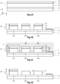
figures 1A à 1H illustrent des étapes d'un procédé de fabrication d'un substrat de croissance, puis d'une matrice de diodes, selon un premier mode de réalisation où l'étape de suppression des portions supérieures à base d'AlGaN est effectué par gravure photoélectrochimique ; - Les
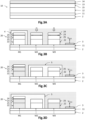
figures 2A à 2D illustrent des étapes d'un procédé de fabrication d'un substrat de croissance, puis d'une matrice de diodes, selon une variante du premier mode de réalisation, où l'empilement cristallin comporte une couche intercalaire de reprise d'épitaxie de faible épaisseur et destinée à ne pas être porosifiée ; - les
figures 3A à 3E illustrent des étapes d'un procédé de fabrication d'un substrat de croissance, puis d'une matrice de diodes, selon une autre variante du premier mode de réalisation, où l'empilement cristallin comporte une couche intercalaire de reprise d'épitaxie destinée à être porosifiée, et pouvant présenter une épaisseur plus importante que dans le cas desfig.2A-2D ; - les
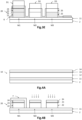
figures 4A à 4F illustrent des étapes d'un procédé de fabrication d'un substrat de croissance, puis d'une matrice de diodes, selon un deuxième mode de réalisation où l'étape de suppression des portions supérieures à base d'AlGaN est effectué par gravure sèche.
- THE
Figures 1A to 1H illustrate steps of a process for manufacturing a growth substrate, then a diode matrix, according to a first embodiment where the step of removing the upper portions based on AlGaN is carried out by photoelectrochemical etching; - THE
Figures 2A to 2D illustrate steps of a process for manufacturing a growth substrate, then a diode matrix, according to a variant of the first embodiment, where the crystalline stack comprises a thin epitaxy recovery interlayer layer and intended not to be porosified; - THE
Figures 3A to 3E illustrate steps of a process for manufacturing a growth substrate, then a diode matrix, according to another variant of the first embodiment, where the crystalline stack comprises an interposed epitaxy recovery layer intended to be porosified, and may have a greater thickness than in the case offig.2A-2D ; - THE
Figures 4A to 4F illustrate steps of a process for manufacturing a growth substrate, then a diode matrix, according to a second embodiment where the step of removing the upper portions based on AlGaN is carried out by dry etching.
Sur les figures et dans la suite de la description, les mêmes références représentent les éléments identiques ou similaires. De plus, les différents éléments ne sont pas représentés à l'échelle de manière à privilégier la clarté des figures. Par ailleurs, les différents modes de réalisation et variantes ne sont pas exclusifs les uns des autres et peuvent être combinés entre eux. Sauf indication contraire, les termes « sensiblement », « environ », « de l'ordre de » signifient à 10% près, et de préférence à 5% près. Par ailleurs, les termes « compris entre ... et ... » et équivalents signifient que les bornes sont incluses, sauf mention contraire.In the figures and in the remainder of the description, the same references represent identical or similar elements. In addition, the different elements are not represented to scale so as to favor the clarity of the figures. Furthermore, the different embodiments and variants are not exclusive of each other and can be combined with each other. Unless otherwise indicated, the terms “substantially”, “approximately”, “of the order of” mean to the nearest 10%, and preferably to the nearest 5%. Furthermore, the terms “between ... and ...” and equivalents mean that the limits are included, unless otherwise stated.
L'invention porte sur un substrat de croissance et son procédé de fabrication. Le substrat de croissance est adapté à la réalisation par épitaxie d'une matrice de diodes à base d'InGaN, les diodes permettant d'émettre ou de détecter, de manière native, un rayonnement lumineux à différentes longueurs d'onde, par exemple de type RGB (rouge, vert, bleu).A growth substrate and method of manufacturing the same are disclosed. The growth substrate is suitable for the production by epitaxy of a matrix of diodes based on InGaN, the diodes making it possible to emit or detect, in a native manner, light radiation at different wavelengths, for example of RGB type (red, green, blue).
Le substrat de croissance comporte des mésas d'au moins trois catégories différentes, notées M1, M2 et M3, ayant différentes déformabilités d1, d2, d3, selon que les mésas comportent ou non une portion supérieure à base d'AIGaN, et selon qu'elles comportent une portion inférieure à base de GaN et/ou une portion de reprise d'épitaxie à base d'InGaN porosifiées ou non. D'une manière générale, la déformabilité est la capacité de la mésa à se déformer lors de la réalisation de la diode.The growth substrate comprises mesas of at least three different categories, denoted M1, M2 and M3, having different deformabilities d1, d2, d3, depending on whether or not the mesas include an upper portion based on AIGaN, and depending on whether They comprise a lower portion based on GaN and/or an epitaxy recovery portion based on InGaN, porosified or not. Generally speaking, deformability is the ability of the mesa to deform during the production of the diode.
Les différentes déformabilités d1, d2, d3 des mésas se traduisent par le fait que les mésas M1, M2, M3 présentent alors différentes valeurs du paramètre de maille effectif, d'une catégorie de mésas à l'autre, au niveau de leur face supérieure, lors de la croissance des diodes. Le paramètre de maille effectif est le paramètre de maille, défini dans un plan principal XY (orthogonal à l'axe de croissance des couches), de la couche ou portion de couche considérée. Aussi, les diodes de catégories D1, D2 et D3, réalisées lors d'une même étape d'épitaxie à partir du substrat de croissance, présenteront des zones actives différentes en termes de proportion d'indium incorporé dans les puits quantiques, et seront donc adaptées à émettre ou détecter un rayonnement lumineux à différentes longueurs d'onde.The different deformabilities d1, d2, d3 of the mesas result in the fact that the mesas M1, M2, M3 then present different values of the effective mesh parameter, from one category of mesas to another, at the level of their upper face , during the growth of the diodes. The effective mesh parameter is the mesh parameter, defined in a main plane XY (orthogonal to the growth axis of the layers), of the layer or portion of layer considered. Also, the diodes of categories D1, D2 and D3, produced during the same epitaxy step from the growth substrate, will present different active zones in terms of proportion of indium incorporated in the quantum wells, and will therefore be adapted to emit or detect light radiation at different wavelengths.
Le procédé de fabrication propose de réaliser tout d'abord des mésas M1, M2, M3 à base de GaN, comportant chacune une portion inférieure à base de GaN, une portion intercalaire dite de séparation à base d'InGaN, et une portion supérieure à base d'AlGaN. Puis, la portion supérieure à base d'AIGaN d'au moins les mésas M3, et éventuellement des mésas M2 également, sont supprimées par gravure, alors qu'elles sont conservées dans les mésas M1. Cette étape de suppression peut être, dans un premier mode de réalisation, effectuée par gravure photoélectrochimique de la portion intercalaire de séparation à base d'InGaN, ou, dans un deuxième mode de réalisation, effectuée par gravure sèche des portions supérieures à base d'AlGaN avec arrêt de gravure sur les portions intercalaires de séparation à base d'InGaN. Le procédé prévoit également de porosifier par porosification électrochimique les portions inférieures des seules mésas M1 et M3, alors qu'elles ne sont pas porosifiées dans les mésas M2.The manufacturing process proposes to first produce mesas M1, M2, M3 based on GaN, each comprising a lower portion based on GaN, an intermediate portion called separation portion based on InGaN, and a portion higher than AlGaN base. Then, the upper AIGaN-based portion of at least the M3 mesas, and possibly the M2 mesas as well, are removed by etching, while they are preserved in the M1 mesas. This removal step can be, in a first embodiment, carried out by photoelectrochemical etching of the intermediate separation portion based on InGaN, or, in a second embodiment, carried out by dry etching of the upper portions based on AlGaN with etching stop on the separation intermediate portions based on InGaN. The process also provides for porosification by electrochemical porosification of the lower portions of the mesas M1 and M3 only, whereas they are not porosified in the mesas M2.
Rappelons que la gravure photoélectrochimique est effectuée en plongeant le substrat de croissance dans un électrolyte liquide, et en éclairant les mésas par un faisceau lumineux d'excitation apte à être absorbé par les seules portions intercalaires de séparation. Le matériau de ces portions intercalaires est alors oxydé et dissous par l'électrolyte liquide. Une faible tension électrique VPECE peut être appliquée pour collecter les électrons photogénérés. Par ailleurs, rappelons également que la porosification électrochimique (porosification par anodisation électrochimique) est effectuée en plongeant également le substrat de croissance dans un électrolyte liquide. Une tension électrique d'une valeur VECE plus élevée est appliquée, provoquant la porosification des portions de couches voulues. Dans le cadre de l'invention, la porosification électrochimique est non-photo-assistée.Remember that the photoelectrochemical etching is carried out by immersing the growth substrate in a liquid electrolyte, and by illuminating the mesas with an excitation light beam capable of being absorbed by the separation intermediate portions alone. The material of these intermediate portions is then oxidized and dissolved by the liquid electrolyte. A low electrical voltage V PECE can be applied to collect the photogenerated electrons. Furthermore, let us also remember that electrochemical porosification (porosification by electrochemical anodization) is carried out by also immersing the growth substrate in a liquid electrolyte. An electrical voltage with a higher value V ECE is applied, causing porosification of the desired layer portions. In the context of the invention, the electrochemical porosification is non-photo-assisted.
Rappelons ici qu'une réaction de porosification électrochimique est une réaction sélective dans le sens où, pour une même tension électrique de valeur VECE, un matériau semiconducteur cristallin à base de GaN sera porosifié si son niveau de dopage ND est supérieur ou égal à un niveau de dopage minimal ND,min(VECE) prédéfini. Dans le cas contraire, il ne sera pas porosifié et restera intègre (dense). A ce titre, le document
On obtient ainsi un substrat de croissance, où :
- ∘ les mésas M2 présentent une déformabilité d2 minimale, dans la mesure où ils ne comportent pas de portions porosifiées. Le paramètre de maille effectif aM2 est celui d'une couche tampon conductrice à base de GaN sur laquelle les mésas reposent (moyennant une légère relaxation liée à la réalisation des mésas). De préférence, on aura donc : aM2 ≈ aGaN ;
- o les mésas M1 présentent une déformabilité d1 supérieure à d2, dans la mesure où elles comportent une portion inférieure à base de GaN porosifiée et une portion supérieure à base d'AlGaN non porosifié. Celle-ci contraint alors les mésas M1 en compression, et conduit à un paramètre de maille effectif aM1, lors de la réalisation des diodes, inférieur à celui des mésas M2 : aM1 < aM2;
- o les mésas M3 présentent également une déformabilité d3 supérieure à d2, dans la mesure où elles comportent une portion inférieure à base de GaN porosifiée. Les mésas M3 comportent également une portion de reprise d'épitaxie à base d'InGaN non porosifié, qui contraint alors les mésas M3 en tension, et conduit à un paramètre de maille effectif aM1, lors de la réalisation des diodes, supérieur à celui des mésas M2 : aM3 > aM2.
- ∘ the M2 mesas have a minimal deformability d2, to the extent that they do not include porosified portions. The effective mesh parameter a M2 is that of a conductive buffer layer based on GaN on which the mesas rest (subject to a slight relaxation linked to the creation of the mesas). Preferably, we will therefore have: a M2 ≈ a GaN ;
- o the mesas M1 have a deformability d1 greater than d2, insofar as they comprise a lower portion based on porosified GaN and an upper portion based on non-porosified AlGaN. This then constrains the mesas M1 in compression, and leads to an effective mesh parameter a M1 , when producing the diodes, lower than that of the mesas M2: a M1 < a M2 ;
- o the M3 mesas also have a deformability d3 greater than d2, to the extent that they include a lower portion based on porosified GaN. The M3 mesas also include an epitaxy recovery portion based on non-porosified InGaN, which then constrains the M3 mesas in voltage, and leads to an effective mesh parameter a M1 , when producing the diodes, greater than that of mesas M2: a M3 > a M2 .
Les
On définit ici et pour la suite de la description un repère direct tridimensionnel orthogonal XYZ, où les axes X et Y forment un plan principal du substrat support 2 et où l'axe Z est orienté suivant l'épaisseur du substrat de croissance 20 en direction des mésas.We define here and for the remainder of the description an orthogonal three-dimensional direct reference XYZ, where the axes X and Y form a main plane of the
En référence à la
Le substrat support 2 est réalisé ici en un matériau non porosifiable, de sorte qu'il reste non poreux (dense) lors de la porosification ultérieure des mésas M1 et M3. Il peut s'agir d'un matériau inerte à la réaction électrochimique de porosification, tel qu'un matériau isolant (saphir...) ou un matériau semiconducteur (SiC, Si...) non intentionnellement dopé (nid) ou faiblement dopé. Il peut également s'agir d'un matériau semiconducteur à base de GaN non intentionnellement dopé ou faiblement dopé pour ne pas être porosifiable à la tension de porosification VECE. A titre d'exemple, la couche support peut être réalisée en saphir, en silicium, en SiC, en GaN autoportant (freestanding en anglais), entre autres. Elle présente une épaisseur par exemple comprise entre 200µm et 1.2mm environ. Des couches intermédiaires peuvent être présentes entre le substrat support 2 et la couche tampon conductrice 11, réalisées par exemple à base d'AIN. Ainsi, à titre d'exemples, on peut utiliser les empilements suivants : Si/AIN/AIGaN/GaN ; saphir/GaN nid ; SiC/AIN/AIGaN etc... Le substrat support 2 peut être absent si la couche tampon conductrice 11 présente une épaisseur suffisante pour assurer la tenue mécanique du substrat de croissance 20.The
L'empilement cristallin 10 comporte une couche tampon conductrice 11, sur laquelle reposeront les mésas M1, M2, M3 et qui permettra d'appliquer un potentiel électrique aux portions inférieures 22 des mésas à partir d'une électrode de polarisation 3. Pour cela, la couche tampon conductrice 11 est réalisée en un matériau cristallin à base de GaN dopé (ici de type n) sur au moins une partie de son épaisseur, avec par exemple un niveau de dopage de 1018 cm-3. La couche tampon conductrice 11 est réalisée par épitaxie à partir du substrat support 2. Elle peut présenter une épaisseur comprise entre 1 et 10µm environ. Avec ce niveau de dopage, la couche tampon conductrice 11 n'est pas porosifiée lors de l'étape ultérieure de porosification électronique (à la tension électrique de l'ordre de 15V environ), et permet la circulation des porteurs de charge.The
La couche inférieure 12 repose sur la couche tampon conductrice 11 et est en contact électrique avec elle (et ici en contact physique). Elle est destinée à former les portions inférieures 22 des mésas, dont seules les portions inférieures 22 des mésas M1 et M3 seront porosifiées. Elle est réalisée à base de GaN, et peut, d'une manière générale, être réalisée en InxGa1-xN avec une proportion d'indium x, positive ou nulle, inférieure à celle de la couche intercalaire de séparation 13 pour ne pas absorber le faisceau lumineux d'excitation lors de l'étape ultérieure de gravure photoélectrochimique. Elle est dopée suffisamment pour que les portions inférieures 22 des mésas M1 et M3 soient porosifiées lors de l'étape ultérieure de porosification électrochimique. Dans cet exemple, elle est réalisée en GaN dopé de type n avec un niveau de dopage de 6×1018 cm-3 environ. Son épaisseur est de l'ordre de plusieurs centaines de nanomètres pour permettre une bonne relaxation des contraintes mécaniques des mésas M1 et M3, par exemple au moins égale à 500nm, et est ici égale à 1000nm environ.The
La couche intercalaire de séparation 13 repose sur la couche inférieure 12, et est ici en contact avec elle. Elle est destinée à être gravée, lors de l'étape ultérieure de gravure photoélectrochimique, pour assurer le retrait des portions supérieures 24 des seules mésas M2 et M3 (et non pas des mésas M1). Il s'agit donc d'une couche sacrificielle. Elle est réalisée à base d'InxGa1-xN, avec une proportion d'indium x non nulle supérieure à celles des couches inférieure 12 et supérieure 14, par exemple comprise entre 10 et 15%, pour être la seule à absorber le faisceau lumineux d'excitation lors de l'étape ultérieure de gravure photoélectrochimique. Autrement dit, son énergie de bande interdite est inférieure à celle des couches inférieure 12 et supérieure 14. Dans cet exemple, elle est réalisée en InGaN non intentionnellement dopé, avec une proportion d'indium x de 15% environ. Son épaisseur est de l'ordre de quelques nanomètres, par exemple de 3nm environ. Elle peut ainsi former un unique puits quantique ou plusieurs puits quantiques. Notons que l'InGaN se porosifie à une tension électrique VECE plus faible que celle du GaN, à niveau de dopage équivalent. La proportion d'indium x et le niveau de dopage sont choisis ici pour que la portion intercalaire de séparation 23 ne soit pas porosifiée lors de l'étape de porosification de la
La couche supérieure 14 repose sur la couche intercalaire de séparation 13, et est ici en contact avec elle. Elle est destinée à former les portions supérieures 24 des mésas, dont celle des mésas M3 sera supprimée (et ici également celle des mésas M2) lors de l'étape ultérieure de gravure photoélectrochimique, et celle des mésas M1 sera conservée. Elle est réalisée à base d'AlyGa1-yN, avec une proportion d'aluminium y non nulle, supérieure à celles des couches inférieure 12 et intercalaire 13. Le niveau de dopage est choisi pour que la portion supérieure 24 des mésas M1 ne soit pas porosifiée lors de l'étape ultérieure de porosification électrochimique. Le matériau peut donc être non intentionnellement dopé ou faiblement dopé. Dans cet exemple, elle est réalisée en AlGaN non intentionnellement dopé avec une proportion d'aluminium y de 10% environ. Son épaisseur est de l'ordre de la centaine de nanomètres, par exemple de 100nm environ. Notons que la couche supérieure 14 peut être recouverte d'une fine couche de protection (non représentée), par exemple en GaN ou en InGaN d'une épaisseur de l'ordre de 1 à 3nm, pour éviter l'oxydation de l'AIGaN.The
Notons ici que les couches inférieure 12, intercalaire 13 et supérieure 14 présentent chacune une épaisseur inférieure à leur épaisseur critique à laquelle il y a une relaxation plastique des contraintes mécaniques. L'épaisseur totale de l'empilement cristallin 10 est également inférieure à une épaisseur critique prédéfinie. Ainsi, la couche tampon conductrice 11 génère, dans les couches inférieure 12, intercalaire 13 et supérieure 14, des contraintes mécaniques (orientées dans le plan XY) dont la valeur est telle que, avant porosification, le paramètre de maille effectif est proche ou sensiblement égal au paramètre de maille effectif de la couche tampon conductrice 11, ici sensiblement égal à celui du GaN relaxé (ou légèrement en compression s'il est réalisé à partir du saphir).Note here that the lower 12, intermediate 13 and upper 14 layers each have a thickness less than their critical thickness at which there is a plastic relaxation of the mechanical stresses. The total thickness of the
En référence à la
On dépose ensuite une électrode de polarisation 3 sur et au contact de la couche tampon conductrice 11, qui permettra d'appliquer un potentiel électrique aux mésas.A
En référence à la
Pour cela, on dépose tout d'abord la couche d'encapsulation 4 sur les mésas M1, de manière à les recouvrir entièrement. Les mésas M2 et M3 ne sont pas recouverte pas cette couche 4. Ce peut être une résine photosensible, voir une couche conforme d'un oxyde. La portion intercalaire 23 des mésas M1 ne sera donc pas en contact avec l'électrolyte liquide.To do this, the
Ensuite, on effectue la gravure des portions intercalaires 23 des mésas M2 et M3. On plonge le substrat de croissance 20 dans un électrolyte liquide permettant de dissoudre l'InGaN oxydé formé par l'absorption du faisceau lumineux d'excitation. L'électrolyte liquide peut être acide ou basique, et peut être de l'acide oxalique. Il peut également s'agir de KOH, HF, HNO3, NaNO3, H2SO4 ou de leur mélange. On peut ainsi utiliser également un mélange d'acide oxalique et de NaNO3. On soumet également le substrat de croissance 20 à un faisceau lumineux d'excitation dont le spectre permet de n'exciter que la portion intercalaire 23. Il peut s'agir d'une lampe de lumière blanche associée à un filtre, d'une LED, voire d'une source laser. Ainsi, un laser à 405nm peut être utilisé pour n'exciter que les portions intercalaires 23 en InGaN à 15% d'indium. Par ailleurs, une tension électrique VPECE peut être appliquée par un générateur électrique entre l'électrode de polarisation et une contre-électrode insérée dans l'électrolyte (par exemple, un fil ou une grille de platine). Elle peut être égale par exemple à 2V. Cette tension électrique VPECE permet d'améliorer la collection des électrons photogénérés.Then, we carry out the engraving of the
En référence à la
En référence à la
Ensuite, on plonge à nouveau le substrat de croissance 20 dans un électrolyte liquide. L'électrode de polarisation 3 est alors connectée au générateur électrique de manière à appliquer une tension électrique de valeur VECE, par exemple ici égale à 15V. Cela se traduit par une porosification des portions inférieures 22 des mésas M1 et M3, qui seules sont au contact de l'électrolyte liquide. La portion inférieure 22 de la mésa M2n'est donc pas porosifiée. La tension électrique peut être appliquée pendant une durée allant de quelques secondes à quelques heures. Une électrode de référence peut être utilisée pour contrôler précisément la tension électrique appliquée. Au cours de cette étape, il n'y a pas d'émission du faisceau lumineux d'excitation en direction des mésas. On retire ensuite le substrat de croissance 20 du bain électrolytique, et on retire la couche d'encapsulation 5.Then, the
Ainsi, on obtient un substrat de croissance 20, dont les mésas, qui présentent différentes déformabilités, ont été obtenues à partir d'un même empilement cristallin 10 initial. Il est donc adapté à la réalisation par épitaxie d'une matrice de diodes permettant d'émettre ou de recevoir un rayonnement lumineux à différentes longueurs d'onde de manière native, en particulier après avoir réalisé des portions de reprise d'épitaxie 27 à base d'InGaN.Thus, we obtain a
Ainsi, les mésas M2 présentent une déformabilité d2 minimale, par le fait qu'elle n'est pas porosifiée. Dans cet exemple, elle ne comporte plus la portion supérieure 24 à base d'AlGaN. En variante, comme indiqué précédemment, elle pourrait l'avoir gardée, auquel cas la portion supérieure 24 serait non porosifiée (comme la portion inférieure 22). Quoi qu'il en soit, les mésas M2 présentent un paramètre de maille effectif qui est sensiblement égal à celui de la couche tampon conductrice 11, voire est sensiblement égal au paramètre de maille du matériau relaxé de la couche 11, du fait de la faible relaxation des mésas lors de leur réalisation (
Les mésas M1 présentent une déformabilité d1 supérieure à d2 du fait de la porosification de la portion inférieure 22. De plus, la portion inférieure 22 porosifiée permet aux mésas M1 de relaxer sous l'effet des contraintes mécaniques en compression générées par la portion supérieure 24 à base d'AlGaN non porosifié, de sorte que le paramètre de maille effectif est alors inférieur à celui des mésas M2. Cependant, après cette relaxation, la portion 24 va limiter la déformation de la mésa M1 lors de la réalisation des diodes, et donc limiter l'incorporation d'indium. Les mésas M1 permettront la réalisation de diodes D1 émettant par exemple dans le bleu.The M1 mesas have a deformability d1 greater than d2 due to the porosification of the
Enfin, les mésas M3 présentent une déformabilité d3 supérieure à d2 et différente de d1, du fait de la porosification de la portion inférieure 22 et à l'absence de la portion supérieure 24 à base d'AlGaN. Les mésas M3 pourront présenter, lors de la réalisation de la portion de reprise d'épitaxie 27 à base d'InGaN, un paramètre de maille effectif supérieur à celui des mésas M2 du fait des contraintes mécaniques en tension générées par la portion 27. Les mésas M3 permettront la réalisation de diodes D3 émettant par exemple dans le rouge.Finally, the mesas M3 have a deformability d3 greater than d2 and different from d1, due to the porosification of the
En référence à la
En référence à la
Ensuite, on réalise des portions de reprise d'épitaxie 27 sur les mésas M1, M2 et M3 et en particulier sur celle des mésas M3. Ces portions 27 peuvent présenter une épaisseur de 200nm environ et peuvent être réalisées en InGaN avec une proportion d'indium de l'ordre de 8% environ. La portion de reprise d'épitaxie 27 provoque alors la déformation de la portion inférieure 22 porosifiée des mésas M3 (contraintes en tension), qui en retour permettent aux portions de reprise d'épitaxie 27 de relaxer. De plus, le paramètre de maille au niveau de la face supérieure des mésas M3 est différent de celui des mésas M1.Then,
En référence à la
Ainsi, le procédé de fabrication permet de réaliser de manière native des diodes D1, D2, D3 qui émettront à des longueurs d'onde différentes, ici dans les trois couleurs RGB. Ceci est possible par le fait que les mésas M1, M2, M3 présentent des déformabilités différentes d1, d2, d3. Aussi, l'incorporation d'indium dans les diodes, et en particulier dans les premières portions dopées n puis dans les puits quantiques des zones actives, dépend en effet de la déformabilité des mésas et du paramètre de maille effectif. Plus le paramètre de maille effectif de la portion de reprise d'épitaxie est important (après réalisation des diodes), plus la longueur d'onde principale de la diode correspondante sera grande. Le procédé de fabrication du substrat de croissance 20 met ainsi en jeu une étape de gravure photoélectrochimique, et au moins une étape de porosification électrochimique. Il n'a donc pas été besoin d'effectuer, comme dans l'art antérieur mentionné plus haut, des étapes d'implantation ionique localisée de dopants pour obtenir les différents types de mésas.Thus, the manufacturing process makes it possible to natively produce diodes D1, D2, D3 which will emit at different wavelengths, here in the three RGB colors. This is possible by the fact that the mesas M1, M2, M3 have different deformabilities d1, d2, d3. Also, the incorporation of indium in the diodes, and in particular in the first n-doped portions then in the quantum wells of the active zones, depends in fact on the deformability of the mesas and the effective mesh parameter. The greater the effective mesh parameter of the epitaxy recovery portion (after production of the diodes), the greater the main wavelength of the corresponding diode will be. The process for manufacturing the
Les
En référence à la
En référence à la
En référence à la
En référence à la
Les
En référence à la
En référence à la
En référence à la
En référence à la
En référence à la
Les
En référence à la
En référence à la
On effectue ensuite une deuxième étape de gravure sèche, par exemple par gravure RIE avec un deuxième agent de gravure. Un masque de gravure 7 (masque dur) est déposé pour recouvrir les mésas M1 et laisser libre la face supérieure d'au moins les mésas M3, et ici également celle des mésas M2. Il peut également recouvrir la face libre de la couche tampon conductrice 11. Ici, le deuxième agent de gravure est choisi pour être en mesure de graver localement les portions supérieures 24 à base d'AIGaN des mésas M2 et M3, et s'arrêter sur les portions intercalaires 23. Ensuite, le masque dur 7 est retiré. A la suite de cette étape, la face supérieure des mésas M1 est formée par la portion supérieure 24 à base d'AlGaN non porosifié, et celles des mésas M2 et M3 sont formées par la portion intercalaire 23 encore présente (qui peut être gravée sur une partie de son épaisseur, en fonction des conditions opératoires de la gravure sèche).A second dry etching step is then carried out, for example by RIE etching with a second etching agent. An etching mask 7 (hard mask) is deposited to cover the M1 mesas and leave the upper face of at least the M3 mesas free, and here also that of the M2 mesas. It can also cover the free face of the
En référence à la
En référence à la
En référence à la
En référence à la
Des modes de réalisation particuliers viennent d'être décrits. Différentes variantes et modifications apparaîtront à l'homme du métier.Particular embodiments have just been described. Different variants and modifications will appear to those skilled in the art.
Ainsi, comme décrit précédemment, la portion supérieure 24 des mésas M2 peut être gardée, comme pour les mésas M1. Par ailleurs, la ou les étapes de porosification électrochimique non photo-assistée peuvent être réalisées avant l'étape de suppression de la portion supérieure 24 d'au moins la mésa M3. Enfin, les portions de reprise d'épitaxie 25, 27 peuvent être réalisées avant ou pendant l'étape de réalisation des diodes. Lorsqu'elles sont réalisées avant celle des diodes, elles peuvent être porosifiées, auquel cas elles présentent une épaisseur faible, ou elles peuvent ne pas être porosifiées, auquel cas elles peuvent présenter une épaisseur plus importante.Thus, as described previously, the
Claims (13)
Applications Claiming Priority (1)
| Application Number | Priority Date | Filing Date | Title |
|---|---|---|---|
| FR2214167A FR3144485B1 (en) | 2022-12-21 | 2022-12-21 | Method for manufacturing a growth substrate comprising mesas of different deformabilities, by etching and electrochemical porosification |
Publications (1)
| Publication Number | Publication Date |
|---|---|
| EP4398317A1 true EP4398317A1 (en) | 2024-07-10 |
Family
ID=85685553
Family Applications (1)
| Application Number | Title | Priority Date | Filing Date |
|---|---|---|---|
| EP23218208.9A Pending EP4398317A1 (en) | 2022-12-21 | 2023-12-19 | Process for manufacturing a growth substrate comprising mesas with different deformability, by electrochemical etching and porosification |
Country Status (4)
| Country | Link |
|---|---|
| US (1) | US20240213398A1 (en) |
| EP (1) | EP4398317A1 (en) |
| CN (1) | CN118231532A (en) |
| FR (1) | FR3144485B1 (en) |
Citations (4)
| Publication number | Priority date | Publication date | Assignee | Title |
|---|---|---|---|---|
| EP3840016A1 (en) | 2019-12-19 | 2021-06-23 | Commissariat à l'énergie atomique et aux énergies alternatives | Method for manufacturing a substrate comprising a relaxed ingan layer |
| EP3840065A1 (en) | 2019-12-19 | 2021-06-23 | Commissariat à l'énergie atomique et aux énergies alternatives | Method for manufacturing a relaxed gan/ingan structure |
| US20220285584A1 (en) * | 2021-03-08 | 2022-09-08 | Applied Materials, Inc. | Indium-gallium-nitride light emitting diodes with light reflecting mirrors |
| CN115483321A (en) * | 2021-06-16 | 2022-12-16 | 法国原子能源和替代能源委员会 | Method for manufacturing natural emission matrix |
Family Cites Families (6)
| Publication number | Priority date | Publication date | Assignee | Title |
|---|---|---|---|---|
| FR3099966B1 (en) * | 2019-08-16 | 2021-09-24 | Commissariat Energie Atomique | Manufacturing process of optoelectronic devices |
| TW202211498A (en) * | 2020-08-04 | 2022-03-16 | 英商普羅科技有限公司 | Led device and method of manufacture |
| DE102020128679A1 (en) * | 2020-10-30 | 2022-05-05 | OSRAM Opto Semiconductors Gesellschaft mit beschränkter Haftung | OPTOELECTRONIC DEVICE AND METHOD OF MAKING A SEMICONDUCTOR BODY |
| US20220208848A1 (en) * | 2020-12-30 | 2022-06-30 | Facebook Technologies, Llc | Engineered wafer with selective porosification for multi-color light emission |
| US12336326B2 (en) * | 2022-06-12 | 2025-06-17 | Mikro Mesa Technology Co., Ltd. | Method of manufacturing micro devices |
| FR3141558B1 (en) * | 2022-10-28 | 2025-12-05 | Commissariat Energie Atomique | Diode matrix growth substrate, comprising mesas exhibiting different levels of porification |
-
2022
- 2022-12-21 FR FR2214167A patent/FR3144485B1/en active Active
-
2023
- 2023-12-19 US US18/545,026 patent/US20240213398A1/en active Pending
- 2023-12-19 EP EP23218208.9A patent/EP4398317A1/en active Pending
- 2023-12-21 CN CN202311768150.2A patent/CN118231532A/en active Pending
Patent Citations (5)
| Publication number | Priority date | Publication date | Assignee | Title |
|---|---|---|---|---|
| EP3840016A1 (en) | 2019-12-19 | 2021-06-23 | Commissariat à l'énergie atomique et aux énergies alternatives | Method for manufacturing a substrate comprising a relaxed ingan layer |
| EP3840065A1 (en) | 2019-12-19 | 2021-06-23 | Commissariat à l'énergie atomique et aux énergies alternatives | Method for manufacturing a relaxed gan/ingan structure |
| US20220285584A1 (en) * | 2021-03-08 | 2022-09-08 | Applied Materials, Inc. | Indium-gallium-nitride light emitting diodes with light reflecting mirrors |
| CN115483321A (en) * | 2021-06-16 | 2022-12-16 | 法国原子能源和替代能源委员会 | Method for manufacturing natural emission matrix |
| FR3124313A1 (en) * | 2021-06-16 | 2022-12-23 | Commissariat A L'energie Atomique Et Aux Energies Alternatives | METHOD FOR MANUFACTURING A NATIVE EMISSION MATRIX |
Non-Patent Citations (1)
| Title |
|---|
| GRIFFINOLIVER: "Porous nitride semiconductors reviewed,", J. PHYS. D: APPL. PHYS., vol. 53, 2020, pages 383002 |
Also Published As
| Publication number | Publication date |
|---|---|
| US20240213398A1 (en) | 2024-06-27 |
| CN118231532A (en) | 2024-06-21 |
| FR3144485B1 (en) | 2024-12-13 |
| FR3144485A1 (en) | 2024-06-28 |
Similar Documents
| Publication | Publication Date | Title |
|---|---|---|
| EP3840016A1 (en) | Method for manufacturing a substrate comprising a relaxed ingan layer | |
| EP3503222B1 (en) | Method for manufacturing an optoelectronic device by transferring a conversion structure onto an emission structure | |
| EP4418308A2 (en) | Method for fabricating relaxed gan/gan structure | |
| FR2967813A1 (en) | METHOD FOR PRODUCING A BENTALLIC METAL LAYER STRUCTURE | |
| EP4105999B1 (en) | Method for manufacturing a matrix with native transmission | |
| EP4379800B1 (en) | Method for manufacturing by different electrochemical porosification a growth substrate comprising mesas having different porosification levels | |
| FR3026558A1 (en) | METHOD FOR ACTIVATING DOPANTS IN A SEMICONDUCTOR LAYER BASED ON GAN | |
| EP4362101B1 (en) | Diode array growth substrate with mesas having different porosification levels | |
| EP4383359A1 (en) | Method for porosification of (al,in,ga)n/(al,in,ga)n mesas and resulting structure | |
| EP3563426B1 (en) | Method for producing an optoelectronic device comprising a step of etching the rear face of the growth substrate | |
| FR3143850A1 (en) | Process for producing an electronic device | |
| EP3853882B1 (en) | Method for manufacturing an electronic device | |
| EP4521891A1 (en) | Method for porosification of mesas (al,in,ga)n/(al,in,ga)n | |
| WO2014154993A1 (en) | Process for manufacturing a multi-junction structure for a photovoltaic cell | |
| FR3144485A1 (en) | Process for manufacturing a growth substrate comprising mesas of different deformabilities, by etching and electrochemical porosification | |
| EP4639638A1 (en) | Method for porosifiying a mesa for establishment of contact | |
| EP4102579A1 (en) | Method for manufacturing a substrate comprising a relaxed ingan layer and resulting substrate for resuming growth of a led structure | |
| EP3903341B1 (en) | Method for manufacturing a substrate for a front-facing image sensor | |
| EP4679983A1 (en) | Method of manufacturing a photonic device and corresponding photonic device | |
| EP4391064B1 (en) | Method for manufacturing micro-leds and resulting structure with micro-leds | |
| FR3154229A1 (en) | Process for growing a III-N material | |
| WO2024141738A1 (en) | Method for manufacturing an image sensor |
Legal Events
| Date | Code | Title | Description |
|---|---|---|---|
| PUAI | Public reference made under article 153(3) epc to a published international application that has entered the european phase |
Free format text: ORIGINAL CODE: 0009012 |
|
| STAA | Information on the status of an ep patent application or granted ep patent |
Free format text: STATUS: REQUEST FOR EXAMINATION WAS MADE |
|
| 17P | Request for examination filed |
Effective date: 20231219 |
|
| AK | Designated contracting states |
Kind code of ref document: A1 Designated state(s): AL AT BE BG CH CY CZ DE DK EE ES FI FR GB GR HR HU IE IS IT LI LT LU LV MC ME MK MT NL NO PL PT RO RS SE SI SK SM TR |
|
| RAP3 | Party data changed (applicant data changed or rights of an application transferred) |
Owner name: COMMISSARIAT A L'ENERGIE ATOMIQUE ET AUX ENERGIESALTERNATIVES |