EP4398301A2 - Substrate for display device and display device including the same - Google Patents
Substrate for display device and display device including the same Download PDFInfo
- Publication number
- EP4398301A2 EP4398301A2 EP24178116.0A EP24178116A EP4398301A2 EP 4398301 A2 EP4398301 A2 EP 4398301A2 EP 24178116 A EP24178116 A EP 24178116A EP 4398301 A2 EP4398301 A2 EP 4398301A2
- Authority
- EP
- European Patent Office
- Prior art keywords
- electrode
- tft
- display device
- gate
- insulation film
- Prior art date
- Legal status (The legal status is an assumption and is not a legal conclusion. Google has not performed a legal analysis and makes no representation as to the accuracy of the status listed.)
- Pending
Links
Images



Classifications
-
- G—PHYSICS
- G09—EDUCATION; CRYPTOGRAPHY; DISPLAY; ADVERTISING; SEALS
- G09G—ARRANGEMENTS OR CIRCUITS FOR CONTROL OF INDICATING DEVICES USING STATIC MEANS TO PRESENT VARIABLE INFORMATION
- G09G3/00—Control arrangements or circuits, of interest only in connection with visual indicators other than cathode-ray tubes
- G09G3/20—Control arrangements or circuits, of interest only in connection with visual indicators other than cathode-ray tubes for presentation of an assembly of a number of characters, e.g. a page, by composing the assembly by combination of individual elements arranged in a matrix no fixed position being assigned to or needed to be assigned to the individual characters or partial characters
- G09G3/22—Control arrangements or circuits, of interest only in connection with visual indicators other than cathode-ray tubes for presentation of an assembly of a number of characters, e.g. a page, by composing the assembly by combination of individual elements arranged in a matrix no fixed position being assigned to or needed to be assigned to the individual characters or partial characters using controlled light sources
- G09G3/30—Control arrangements or circuits, of interest only in connection with visual indicators other than cathode-ray tubes for presentation of an assembly of a number of characters, e.g. a page, by composing the assembly by combination of individual elements arranged in a matrix no fixed position being assigned to or needed to be assigned to the individual characters or partial characters using controlled light sources using electroluminescent panels
- G09G3/32—Control arrangements or circuits, of interest only in connection with visual indicators other than cathode-ray tubes for presentation of an assembly of a number of characters, e.g. a page, by composing the assembly by combination of individual elements arranged in a matrix no fixed position being assigned to or needed to be assigned to the individual characters or partial characters using controlled light sources using electroluminescent panels semiconductive, e.g. using light-emitting diodes [LED]
- G09G3/3208—Control arrangements or circuits, of interest only in connection with visual indicators other than cathode-ray tubes for presentation of an assembly of a number of characters, e.g. a page, by composing the assembly by combination of individual elements arranged in a matrix no fixed position being assigned to or needed to be assigned to the individual characters or partial characters using controlled light sources using electroluminescent panels semiconductive, e.g. using light-emitting diodes [LED] organic, e.g. using organic light-emitting diodes [OLED]
- G09G3/3225—Control arrangements or circuits, of interest only in connection with visual indicators other than cathode-ray tubes for presentation of an assembly of a number of characters, e.g. a page, by composing the assembly by combination of individual elements arranged in a matrix no fixed position being assigned to or needed to be assigned to the individual characters or partial characters using controlled light sources using electroluminescent panels semiconductive, e.g. using light-emitting diodes [LED] organic, e.g. using organic light-emitting diodes [OLED] using an active matrix
-
- H—ELECTRICITY
- H10—SEMICONDUCTOR DEVICES; ELECTRIC SOLID-STATE DEVICES NOT OTHERWISE PROVIDED FOR
- H10D—INORGANIC ELECTRIC SEMICONDUCTOR DEVICES
- H10D1/00—Resistors, capacitors or inductors
- H10D1/60—Capacitors
- H10D1/68—Capacitors having no potential barriers
-
- H—ELECTRICITY
- H10—SEMICONDUCTOR DEVICES; ELECTRIC SOLID-STATE DEVICES NOT OTHERWISE PROVIDED FOR
- H10D—INORGANIC ELECTRIC SEMICONDUCTOR DEVICES
- H10D86/00—Integrated devices formed in or on insulating or conducting substrates, e.g. formed in silicon-on-insulator [SOI] substrates or on stainless steel or glass substrates
- H10D86/40—Integrated devices formed in or on insulating or conducting substrates, e.g. formed in silicon-on-insulator [SOI] substrates or on stainless steel or glass substrates characterised by multiple TFTs
- H10D86/421—Integrated devices formed in or on insulating or conducting substrates, e.g. formed in silicon-on-insulator [SOI] substrates or on stainless steel or glass substrates characterised by multiple TFTs having a particular composition, shape or crystalline structure of the active layer
-
- H—ELECTRICITY
- H10—SEMICONDUCTOR DEVICES; ELECTRIC SOLID-STATE DEVICES NOT OTHERWISE PROVIDED FOR
- H10D—INORGANIC ELECTRIC SEMICONDUCTOR DEVICES
- H10D86/00—Integrated devices formed in or on insulating or conducting substrates, e.g. formed in silicon-on-insulator [SOI] substrates or on stainless steel or glass substrates
- H10D86/40—Integrated devices formed in or on insulating or conducting substrates, e.g. formed in silicon-on-insulator [SOI] substrates or on stainless steel or glass substrates characterised by multiple TFTs
- H10D86/421—Integrated devices formed in or on insulating or conducting substrates, e.g. formed in silicon-on-insulator [SOI] substrates or on stainless steel or glass substrates characterised by multiple TFTs having a particular composition, shape or crystalline structure of the active layer
- H10D86/423—Integrated devices formed in or on insulating or conducting substrates, e.g. formed in silicon-on-insulator [SOI] substrates or on stainless steel or glass substrates characterised by multiple TFTs having a particular composition, shape or crystalline structure of the active layer comprising semiconductor materials not belonging to the Group IV, e.g. InGaZnO
-
- H—ELECTRICITY
- H10—SEMICONDUCTOR DEVICES; ELECTRIC SOLID-STATE DEVICES NOT OTHERWISE PROVIDED FOR
- H10D—INORGANIC ELECTRIC SEMICONDUCTOR DEVICES
- H10D86/00—Integrated devices formed in or on insulating or conducting substrates, e.g. formed in silicon-on-insulator [SOI] substrates or on stainless steel or glass substrates
- H10D86/40—Integrated devices formed in or on insulating or conducting substrates, e.g. formed in silicon-on-insulator [SOI] substrates or on stainless steel or glass substrates characterised by multiple TFTs
- H10D86/451—Integrated devices formed in or on insulating or conducting substrates, e.g. formed in silicon-on-insulator [SOI] substrates or on stainless steel or glass substrates characterised by multiple TFTs characterised by the compositions or shapes of the interlayer dielectrics
-
- H—ELECTRICITY
- H10—SEMICONDUCTOR DEVICES; ELECTRIC SOLID-STATE DEVICES NOT OTHERWISE PROVIDED FOR
- H10D—INORGANIC ELECTRIC SEMICONDUCTOR DEVICES
- H10D86/00—Integrated devices formed in or on insulating or conducting substrates, e.g. formed in silicon-on-insulator [SOI] substrates or on stainless steel or glass substrates
- H10D86/40—Integrated devices formed in or on insulating or conducting substrates, e.g. formed in silicon-on-insulator [SOI] substrates or on stainless steel or glass substrates characterised by multiple TFTs
- H10D86/471—Integrated devices formed in or on insulating or conducting substrates, e.g. formed in silicon-on-insulator [SOI] substrates or on stainless steel or glass substrates characterised by multiple TFTs having different architectures, e.g. having both top-gate and bottom-gate TFTs
-
- H—ELECTRICITY
- H10—SEMICONDUCTOR DEVICES; ELECTRIC SOLID-STATE DEVICES NOT OTHERWISE PROVIDED FOR
- H10D—INORGANIC ELECTRIC SEMICONDUCTOR DEVICES
- H10D86/00—Integrated devices formed in or on insulating or conducting substrates, e.g. formed in silicon-on-insulator [SOI] substrates or on stainless steel or glass substrates
- H10D86/40—Integrated devices formed in or on insulating or conducting substrates, e.g. formed in silicon-on-insulator [SOI] substrates or on stainless steel or glass substrates characterised by multiple TFTs
- H10D86/481—Integrated devices formed in or on insulating or conducting substrates, e.g. formed in silicon-on-insulator [SOI] substrates or on stainless steel or glass substrates characterised by multiple TFTs integrated with passive devices, e.g. auxiliary capacitors
-
- H—ELECTRICITY
- H10—SEMICONDUCTOR DEVICES; ELECTRIC SOLID-STATE DEVICES NOT OTHERWISE PROVIDED FOR
- H10D—INORGANIC ELECTRIC SEMICONDUCTOR DEVICES
- H10D86/00—Integrated devices formed in or on insulating or conducting substrates, e.g. formed in silicon-on-insulator [SOI] substrates or on stainless steel or glass substrates
- H10D86/40—Integrated devices formed in or on insulating or conducting substrates, e.g. formed in silicon-on-insulator [SOI] substrates or on stainless steel or glass substrates characterised by multiple TFTs
- H10D86/60—Integrated devices formed in or on insulating or conducting substrates, e.g. formed in silicon-on-insulator [SOI] substrates or on stainless steel or glass substrates characterised by multiple TFTs wherein the TFTs are in active matrices
-
- H—ELECTRICITY
- H10—SEMICONDUCTOR DEVICES; ELECTRIC SOLID-STATE DEVICES NOT OTHERWISE PROVIDED FOR
- H10K—ORGANIC ELECTRIC SOLID-STATE DEVICES
- H10K59/00—Integrated devices, or assemblies of multiple devices, comprising at least one organic light-emitting element covered by group H10K50/00
- H10K59/10—OLED displays
- H10K59/12—Active-matrix OLED [AMOLED] displays
- H10K59/121—Active-matrix OLED [AMOLED] displays characterised by the geometry or disposition of pixel elements
- H10K59/1213—Active-matrix OLED [AMOLED] displays characterised by the geometry or disposition of pixel elements the pixel elements being TFTs
-
- H—ELECTRICITY
- H10—SEMICONDUCTOR DEVICES; ELECTRIC SOLID-STATE DEVICES NOT OTHERWISE PROVIDED FOR
- H10K—ORGANIC ELECTRIC SOLID-STATE DEVICES
- H10K59/00—Integrated devices, or assemblies of multiple devices, comprising at least one organic light-emitting element covered by group H10K50/00
- H10K59/10—OLED displays
- H10K59/12—Active-matrix OLED [AMOLED] displays
- H10K59/121—Active-matrix OLED [AMOLED] displays characterised by the geometry or disposition of pixel elements
- H10K59/1216—Active-matrix OLED [AMOLED] displays characterised by the geometry or disposition of pixel elements the pixel elements being capacitors
-
- H—ELECTRICITY
- H10—SEMICONDUCTOR DEVICES; ELECTRIC SOLID-STATE DEVICES NOT OTHERWISE PROVIDED FOR
- H10K—ORGANIC ELECTRIC SOLID-STATE DEVICES
- H10K59/00—Integrated devices, or assemblies of multiple devices, comprising at least one organic light-emitting element covered by group H10K50/00
- H10K59/10—OLED displays
- H10K59/12—Active-matrix OLED [AMOLED] displays
- H10K59/129—Chiplets
-
- H—ELECTRICITY
- H10—SEMICONDUCTOR DEVICES; ELECTRIC SOLID-STATE DEVICES NOT OTHERWISE PROVIDED FOR
- H10K—ORGANIC ELECTRIC SOLID-STATE DEVICES
- H10K59/00—Integrated devices, or assemblies of multiple devices, comprising at least one organic light-emitting element covered by group H10K50/00
- H10K59/10—OLED displays
- H10K59/12—Active-matrix OLED [AMOLED] displays
- H10K59/131—Interconnections, e.g. wiring lines or terminals
-
- G—PHYSICS
- G09—EDUCATION; CRYPTOGRAPHY; DISPLAY; ADVERTISING; SEALS
- G09G—ARRANGEMENTS OR CIRCUITS FOR CONTROL OF INDICATING DEVICES USING STATIC MEANS TO PRESENT VARIABLE INFORMATION
- G09G2310/00—Command of the display device
- G09G2310/02—Addressing, scanning or driving the display screen or processing steps related thereto
- G09G2310/0264—Details of driving circuits
- G09G2310/0297—Special arrangements with multiplexing or demultiplexing of display data in the drivers for data electrodes, in a pre-processing circuitry delivering display data to said drivers or in the matrix panel, e.g. multiplexing plural data signals to one D/A converter or demultiplexing the D/A converter output to multiple columns
-
- H—ELECTRICITY
- H10—SEMICONDUCTOR DEVICES; ELECTRIC SOLID-STATE DEVICES NOT OTHERWISE PROVIDED FOR
- H10D—INORGANIC ELECTRIC SEMICONDUCTOR DEVICES
- H10D30/00—Field-effect transistors [FET]
- H10D30/60—Insulated-gate field-effect transistors [IGFET]
- H10D30/67—Thin-film transistors [TFT]
- H10D30/6729—Thin-film transistors [TFT] characterised by the electrodes
- H10D30/673—Thin-film transistors [TFT] characterised by the electrodes characterised by the shapes, relative sizes or dispositions of the gate electrodes
- H10D30/6731—Top-gate only TFTs
-
- H—ELECTRICITY
- H10—SEMICONDUCTOR DEVICES; ELECTRIC SOLID-STATE DEVICES NOT OTHERWISE PROVIDED FOR
- H10D—INORGANIC ELECTRIC SEMICONDUCTOR DEVICES
- H10D30/00—Field-effect transistors [FET]
- H10D30/60—Insulated-gate field-effect transistors [IGFET]
- H10D30/67—Thin-film transistors [TFT]
- H10D30/674—Thin-film transistors [TFT] characterised by the active materials
- H10D30/6741—Group IV materials, e.g. germanium or silicon carbide
- H10D30/6743—Silicon
- H10D30/6745—Polycrystalline or microcrystalline silicon
-
- H—ELECTRICITY
- H10—SEMICONDUCTOR DEVICES; ELECTRIC SOLID-STATE DEVICES NOT OTHERWISE PROVIDED FOR
- H10D—INORGANIC ELECTRIC SEMICONDUCTOR DEVICES
- H10D30/00—Field-effect transistors [FET]
- H10D30/60—Insulated-gate field-effect transistors [IGFET]
- H10D30/67—Thin-film transistors [TFT]
- H10D30/674—Thin-film transistors [TFT] characterised by the active materials
- H10D30/6755—Oxide semiconductors, e.g. zinc oxide, copper aluminium oxide or cadmium stannate
-
- H—ELECTRICITY
- H10—SEMICONDUCTOR DEVICES; ELECTRIC SOLID-STATE DEVICES NOT OTHERWISE PROVIDED FOR
- H10K—ORGANIC ELECTRIC SOLID-STATE DEVICES
- H10K59/00—Integrated devices, or assemblies of multiple devices, comprising at least one organic light-emitting element covered by group H10K50/00
- H10K59/10—OLED displays
- H10K59/12—Active-matrix OLED [AMOLED] displays
- H10K59/1201—Manufacture or treatment
-
- H—ELECTRICITY
- H10—SEMICONDUCTOR DEVICES; ELECTRIC SOLID-STATE DEVICES NOT OTHERWISE PROVIDED FOR
- H10K—ORGANIC ELECTRIC SOLID-STATE DEVICES
- H10K59/00—Integrated devices, or assemblies of multiple devices, comprising at least one organic light-emitting element covered by group H10K50/00
- H10K59/10—OLED displays
- H10K59/12—Active-matrix OLED [AMOLED] displays
- H10K59/122—Pixel-defining structures or layers, e.g. banks
-
- H—ELECTRICITY
- H10—SEMICONDUCTOR DEVICES; ELECTRIC SOLID-STATE DEVICES NOT OTHERWISE PROVIDED FOR
- H10K—ORGANIC ELECTRIC SOLID-STATE DEVICES
- H10K59/00—Integrated devices, or assemblies of multiple devices, comprising at least one organic light-emitting element covered by group H10K50/00
- H10K59/10—OLED displays
- H10K59/12—Active-matrix OLED [AMOLED] displays
- H10K59/126—Shielding, e.g. light-blocking means over the TFTs
Definitions
- the present disclosure is directed to a substrate for a display device and a display device including the same that substantially obviate one or more problems due to limitations and disadvantages of the related art.
- Embodiments relate to a display device.
- the display device includes a substrate and a pixel on the substrate.
- the pixel includes a first thin-film transistor (TFT) on the substrate, a storage capacitor on the substrate, and a light-emitting device electrically connected to the storage capacitor.
- the first TFT includes a first gate electrode, at least a first part of an interlayer insulation film on the first gate electrode, a first gate insulation film on the first part of the interlayer insulation film, and a first active layer formed of oxide semiconductor on the first gate insulation film.
- the storage capacitor includes a first storage electrode, at least a second part of the interlayer insulation film on the first storage electrode, and a second storage electrode on the second part of the interlayer insulation film. The second storage electrode is physically separated from the first gate insulation film.
- the first TFT further includes a first source electrode and a first drain electrode electrically connected to the first active layer.
- the first source electrode or the first drain electrode may contact a side surface of the first gate insulation film.
- the second gate electrode has a smaller line width than the first gated electrode and the first storage electrode.
- the interlayer insulation film is formed of silicon nitride (SiNx) and the first gate insulation film is formed of silicon oxide (SiOx).
- a second active layer of a second TFT is formed on the substrate.
- a second gate insulation film is formed on the second active layer.
- a second gate electrode is formed on at least a part of the second gate insulation film. The second active layer, the second gate insulation film, and the second gate electrode may be disposed below the interlayer insulation film.
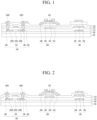
- FIG. 1 is a sectional view illustrating a substrate for a display device according to an embodiment.
- a substrate for a display device shown in FIG. 1 includes first and second thin-film transistors 100 and 150 and a storage capacitor 140.
- the first thin-film transistor 100 having a bottom gate configuration includes a first gate electrode 106, an oxide semiconductor layer 104, a first source electrode 108, and a first drain electrode 110.
- the first gate electrode 106 is formed on a first gate insulation film 112, and may overlap the oxide semiconductor layer 104 with first and second interlayer insulation films 114 and 116 and a second gate insulation film 152 interposed therebetween.
- the first gate electrode 106 is disposed on the first gate insulation film 112, on which a second gate electrode 156 is also disposed, and is formed of the same material as the second gate electrode 156. Accordingly, the first and second gate electrodes 106 and 156 may be formed through the same mask process, and therefore the number of mask processes may be reduced.
- the oxide semiconductor layer 104 is formed on the second gate insulation film 152 so as to overlap the first gate electrode 106, thereby forming a channel between the first source electrode 108 and the first drain electrode 110.
- the oxide semiconductor layer 104 is formed of oxide including at least one metal selected from among Zn, Cd, Ga, In, Sn, Hf, and Zr. Since the first thin-film transistor 100 including this oxide semiconductor layer 104 has advantages of higher electron mobility and lower off-current than the second thin-film transistor 150 including a polycrystalline semiconductor layer 154, it is suitable for application to a switching thin-film transistor, in which an On-time period is short but an Off-time period is long.
- the oxide semiconductor layer 104 may be disposed above the first gate electrode 106 so as to effectively ensure the stability of the device.
- the second gate insulation film 152 which has the same shape as the oxide semiconductor layer 104, is formed between the oxide semiconductor layer 104 and at least a first part of the second interlayer insulation film 116.
- the second gate insulation film 152 may contact the second interlayer insulation film 116.
- the second gate insulation film 152 is formed of a material having a selective etch ratio different from that of the first gate insulation film 112 and the first and second interlayer insulation films 114 and 116.
- the second gate insulation film 152 is formed of SiOx, which is an oxide film
- the first gate insulation film 112 and the first and second interlayer insulation films 114 and 116 are formed of SiNx, which is a nitride film.
- the second interlayer insulation film 116 which is exposed during a dry-etching process for forming the second gate insulation film 152 and the oxide semiconductor layer 104, from being damaged by a dry-etching gas used for the dry-etching process. Further, it is possible to prevent the second gate insulation film 152 and the oxide semiconductor layer 104, which are exposed during a dry-etching process for forming source and drain contact holes 164S and 164D that penetrate the first gate insulation film 112 and the first and second interlayer insulation films 114 and 116, from being damaged by a dry-etching gas used for the dry-etching process.
- the second gate insulation film 152 is an inorganic insulation film formed of, for example, silicon oxide (SiOx), which has lower hydrogen particle content than the first gate insulation film 112. Accordingly, it is possible to prevent hydrogen contained in the first gate insulation film 112 and hydrogen contained in the polycrystalline semiconductor layer 154 from being diffused to the oxide semiconductor layer 104 during a heat treatment process performed on the oxide semiconductor layer 104.
- SiOx silicon oxide
- Each of the first source electrode 108 and the first drain electrode 110 may be a single layer or multiple layers disposed on the second interlayer insulation film 116 and formed of any one selected from among molybdenum (Mo), aluminum (Al), chrome (Cr), gold (Au), titanium (Ti), nickel (Ni), neodymium (Nd), and copper (Cu), or an alloy thereof.
- Mo molybdenum
- Al aluminum
- Cr chrome
- Au gold
- Ti titanium
- Ni nickel
- Nd neodymium
- Cu copper
- the embodiment is not limited thereto.
- the first source electrode 108 and the first drain electrode 110 are formed to face each other with the channel of the oxide semiconductor layer 104 interposed therebetween. Meanwhile, an etch stopper (not shown) may be formed on the oxide semiconductor layer 104 that is exposed between the first source electrode 108 and the first drain electrode 110.
- the second thin-film transistor 150 having a top-gate configuration is disposed on a substrate 101 so as to be spaced apart from the first thin-film transistor 100.
- the second thin-film transistor 150 includes a polycrystalline semiconductor layer 154, a second gate electrode 156, a second source electrode 158, and a second drain electrode 160.
- the polycrystalline semiconductor layer 154 is formed on a buffer layer 102 that covers the substrate 101.
- the polycrystalline semiconductor layer 154 includes a channel region 154C, a source region 154S, and a drain region 154D.
- the channel region 154C overlaps the second gate electrode 156 with the first gate insulation film 112 interposed therebetween, and forms a channel between the second source electrode 158 and the second drain electrode 160.
- the source region 154S is electrically connected to the second source electrode 158 through a source contact hole 164S.
- the drain region 154D is electrically connected to the second drain electrode 160 through a drain contact hole 164D. Since the polycrystalline semiconductor layer 154 has high mobility, low power consumption, and high reliability, it is suitable for applications as a gate-driving unit for driving gate lines and/or to a multiplexer (MUX).
- MUX multiplexer
- the second gate electrode 156 overlaps the channel region 154C of the polycrystalline semiconductor layer with the first gate insulation film 112 interposed therebetween.
- the second gate electrode 156 has a smaller line width than the first gate electrode 106 and the intermediate storage electrode 144.
- the second gate electrode 156 may be a single layer or multiple layers formed of the same material as the first gate electrode 106, e.g. any one selected from among molybdenum (Mo), aluminum (Al), chrome (Cr), gold (Au), titanium (Ti), nickel (Ni), neodymium (Nd), and copper (Cu), or an alloy thereof.
- Mo molybdenum
- Al aluminum
- Cr chrome
- Au gold
- Ti titanium
- Ni nickel
- Nd neodymium
- Cu copper
- the embodiments are not limited thereto.
- the first gate insulation film 112 is positioned on the polycrystalline semiconductor layer 154, and is an inorganic insulation film formed of, for example, silicon nitride (SiNx), which has higher hydrogen particle content than the second gate insulation film 152.
- the hydrogen particles contained in the first gate insulation film 112 are diffused to the polycrystalline semiconductor layer 154 during a hydrogenation process, thereby enabling pores in the polycrystalline semiconductor layer 154 to be filled with hydrogen. Accordingly, the polycrystalline semiconductor layer 154 is stabilized, thus preventing deterioration of the properties of the second thin-film transistor 150.
- the second source electrode 158 is connected to the source region 154S of the polycrystalline semiconductor layer 154 through the source contact hole 164S that penetrates the first gate insulation film 112 and the first and second interlayer insulation films 114 and 116.
- the second drain electrode 160 faces the second source electrode 158, and is connected to the drain region 154D of the polycrystalline semiconductor layer 154 through the drain contact hole 164D that penetrates the first gate insulation film 112 and the first and second interlayer insulation films 114 and 116. Since the second source electrode 158 is in the same layer and is formed of the same material as the first source electrode 108, and since the second drain electrode 160 is in the same layer and is formed of the same material as the first drain electrode 110, the first and second source electrodes 108 and 158 and the first and second drain electrodes 110 and 160 may be formed at the same time through the same mask process.
- the oxide semiconductor layer 104 of the first thin-film transistor 100 is formed. That is, the oxide semiconductor layer 104 is disposed above the polycrystalline semiconductor layer 154. Accordingly, the oxide semiconductor layer 104 is not exposed to the high-temperature atmosphere of the activation and hydrogenation processes of the polycrystalline semiconductor layer 154, thereby preventing damage to the oxide semiconductor layer 104 and therefore improving reliability.
- the storage capacitor 140 includes a first storage capacitor and a second storage capacitor, which are connected in parallel.
- the first storage capacitor is formed such that a lower storage electrode 142 and an intermediate storage electrode 144 overlap each other with the first gate insulation film 112 interposed therebetween.
- the second storage capacitor is formed such that the intermediate storage electrode 144 and an upper storage electrode 146 overlap each other with at least one of the first and second interlayer insulation films 114 and 116 interposed therebetween.
- the lower storage electrode 142 is disposed on the buffer film 102, and is positioned in the same layer and is formed of the same material as the polycrystalline semiconductor layer 154.
- the intermediate storage electrode 144 is disposed on the first gate insulation film 112, and is positioned in the same layer and is formed of the same material as the second gate electrode 156.
- the upper storage electrode 146 is disposed on the second interlayer insulation film 116, and is positioned in the same layer and is formed of the same material as the source and drain electrodes 108, 158, 110, and 160.
- the first gate insulation film 112 and the first and second interlayer insulation films 114 and 116 are formed of an inorganic insulation material such as, for example, SiOx or SiNx.
- At least one of the first gate insulation film 112 and the first and second interlayer insulation films 114 and 116 may be formed of SiNx, which has a higher dielectric constant than SiOx. Accordingly, since the intermediate storage electrode 144 overlaps the lower storage electrode 142, with the first gate insulation film 112, which is formed of SiNx having a relatively high dielectric constant, interposed therebetween, the capacity of the first storage capacitor is increased in proportion to the dielectric constant. Similarly, since the upper storage electrode 146 overlaps the intermediate storage electrode 144 with the first and second interlayer insulation films 114 and 116, which are formed of SiNx having a relatively high dielectric constant, interposed therebetween, the capacity of the second storage capacitor is increased in proportion to the dielectric constant.
- the first and second interlayer insulation film 114 and 116 are interposed between the upper storage electrode 146 and the intermediate storage electrode 144.
- the second gate insulation film 152 over the intermediate storage electrode 144 is eliminated through etching process, and thus the upper storage electrode 146 is placed directly on the second interlayer insulation film 116.
- the upper storage electrode 146 does not contact the second gate insulation film 152, but contacts the second interlayer insulation film 116.
- the second interlayer insulation film 116 may be eliminated, and only the first interlayer insulation film 114, which is formed of SiNx, may be interposed between the upper storage electrode 146 and the intermediate storage electrode 144.
- the substrate for a display device having the above construction according to the present disclosure is applicable to the display device shown in FIG. 3 .
- the display device shown in FIG. 3 includes a display panel 180, a gate-driving unit 182 for driving gate lines GL of the display panel 180, and a data-driving unit 184 for driving data lines DL of the display panel 180.
- the display panel 180 includes a display area AA and a non-display area NA surrounding the display area AA.
- pixels are located at intersecting portions between the gate lines GL and the data lines DL.
- the pixels are arranged in a matrix form.
- Each of the pixels includes the storage capacitor 140 and at least one of the first thin-film transistor 100 and the second thin-film transistor 150.
- the gate-driving unit 182 is disposed in the non-display area NA.
- the gate-driving unit 182 is configured using the second thin-film transistor 150 including the polycrystalline semiconductor layer 154.
- the second thin-film transistor 150 of the gate-driving unit 182 is formed simultaneously with the first and second thin-film transistors 100 and 150 in the display area AA through the same process.
- the second thin-film transistor 150 of the multiplexer 186 may be directly formed on the substrate 101 for a display device together with the second thin-film transistor 150 of the gate-driving unit 182 and the first and second thin-film transistors 100 and 150 in the display area AA.
- the above-described display device is applicable to a display device that requires a thin-film transistor, e.g. the organic light-emitting display device shown in FIG. 4 or a liquid crystal display device.
- the organic light-emitting display device shown in FIG. 4 includes first and second thin-film transistors 100 and 150, a light-emitting diode 130 connected to the second thin-film transistor 150, and a storage capacitor 140.
- the first thin-film transistor 100 including an oxide semiconductor layer 104 is applied to a switching transistor of each pixel located in the display area AA
- the second thin-film transistor 150 including a polycrystalline semiconductor layer 154 is applied to a driving transistor of each pixel located in the display area AA
- the first thin-film transistor 100 including the oxide semiconductor layer 104 may be applied to a switching transistor for switching data voltage input to each pixel located in the display area AA and to a driving transistor connected to each light-emitting diode 130.
- the second thin-film transistor 150 including the polycrystalline semiconductor layer 154 is applied to a transistor of a driving circuit of at least one of the gate-driving unit 182 located in the non-display area NA and the multiplexer 186.
- the storage capacitor 140 includes a lower storage electrode 142, which is disposed on a buffer film 102, and an intermediate storage electrode 144, which overlaps the lower storage electrode 142 with a first gate insulation film 112 interposed therebetween.
- the lower storage electrode 142 is positioned in the same layer and is formed of the same material as the polycrystalline semiconductor layer 154, and the intermediate storage electrode 144 is positioned in the same layer and is formed of the same material as a second gate electrode 156. As shown in FIG.
- the intermediate storage electrode 144 is connected to a drain electrode 110 of any one of the switching transistor and the driving transistor through a first storage contact hole 148a, and the lower storage electrode 142 and the upper storage electrode 146 are connected to a drain electrode 160 of the remaining one of the switching transistor and the driving transistor through a second storage contact hole 148b.
- the light-emitting diode 130 is a light-emitting device, and includes an anode 132, which is connected to the second drain electrode 160 of the second thin-film transistor 150, at least one light-emitting stack 134, which is formed on the anode 132, and a cathode 136, which is formed on the light-emitting stack 134.
- the anode 132 is connected to a pixel connection electrode 124, which is exposed through a second pixel contact hole 120 that penetrates a planarization layer 128.
- the pixel connection electrode 124 is connected to the second drain electrode 160, which is exposed through a first pixel contact hole 122 that penetrates first and second protective films 118 and 126.
- the anode 132 is formed in a multilayer structure including a transparent conductive film and an opaque conductive film having high reflection efficiency.
- the transparent conductive film is formed of a material having a relatively high work function, e.g.
- the opaque conductive film is formed in a single-layer or multilayer structure including any one selected from among Al, Ag, Cu, Pb, Mo, and Ti or an alloy thereof.
- the anode 132 may be formed in a structure such that a transparent conductive film, an opaque conductive film and a transparent conductive film are sequentially stacked, or such that a transparent conductive film and an opaque conductive film are sequentially stacked.
- the polycrystalline semiconductor layer 154 and the lower storage electrode 142 are formed by patterning the polycrystalline silicon thin film through a photolithography process using a first mask and an etching process. Subsequently, the lower storage electrode 142, excluding the polycrystalline semiconductor layer 154, is selectively doped with impurities through a photolithography process using a second mask, thereby forming the lower storage electrode 142 having conductivity.
- the first and second protective films 118 and 126 are sequentially formed on the substrate 101, on which the first and second source electrodes 108 and 158, the first and second drain electrodes 110 and 160 and the upper storage electrode 146 have been formed, through a deposition process.
- the first and second protective films 118 and 126 are formed of an inorganic insulation material such as SiOx or SiNx or an organic insulation material such as an acrylic resin.
- the first and second protective films 118 and 126 are patterned through a photolithography process using a seventh mask and an etching process, thereby forming the first pixel contact hole 122.
Landscapes
- Engineering & Computer Science (AREA)
- Microelectronics & Electronic Packaging (AREA)
- Physics & Mathematics (AREA)
- Geometry (AREA)
- Computer Hardware Design (AREA)
- General Physics & Mathematics (AREA)
- Theoretical Computer Science (AREA)
- Devices For Indicating Variable Information By Combining Individual Elements (AREA)
- Electroluminescent Light Sources (AREA)
- Chemical & Material Sciences (AREA)
- Crystallography & Structural Chemistry (AREA)
- Thin Film Transistor (AREA)
Abstract
Description
- This application claims priority to Republic of
Korea Patent Application No. 10-2016-0174261, filed on December 20, 2016 - The present disclosure relates to a substrate for a display device and a display device including the same, and more particularly to a substrate for a display device, which is capable of realizing lower power consumption and a larger area, and a display device including the same.
- An image display device, which displays various kinds of information on a screen, is a core technology of the information and communication age, and is currently being developed with the aims of a thinner and lighter design, greater portability, and higher performance. Hence, flat panel display devices, which may reduce the disadvantageously heavy weight and volume of a cathode ray tube (CRT), are in the spotlight.
- Examples of flat panel display devices include liquid crystal display (LCD) devices, plasma display panel (PDP) devices, organic light-emitting display (OLED) devices, and electrophoretic display (ED) devices.
- A flat panel display device includes thin-film transistors arranged in pixels. In order to apply a display device to portable appliances, low power consumption is required. However, it is difficult to realize low power consumption with technologies related to display devices that have been developed to date.
- Accordingly, the present disclosure is directed to a substrate for a display device and a display device including the same that substantially obviate one or more problems due to limitations and disadvantages of the related art.
- An object is to provide a substrate for a display device, which is capable of realizing lower power consumption and a larger area, and a display device including the same.
- Additional advantages, objects, and features will be set forth in part in the description which follows and in part will become apparent to those having ordinary skill in the art upon examination of the following or may be learned from practice of the disclosure. The objectives and other advantages may be realized and attained by the structure particularly pointed out in the written description and claims hereof as well as the appended drawings. Aspects of an invention are defined in the appended claims.
- There is provided a substrate for a display device including a first thin-film transistor including an oxide semiconductor layer, a second thin-film transistor spaced apart from the first thin-film transistor and including a polycrystalline semiconductor layer, and a storage capacitor including at least two storage electrodes. One of the at least two storage electrodes is located in the same plane and is formed of the same material as gate electrodes of the first thin-film transistor and the second thin-film transistor, and another one of the at least two storage electrodes is located in the same plane and is formed of the same material as source and drain electrodes of the first thin-film transistor and the second thin-film transistor.
- Embodiments relate to a display device. The display device includes a substrate and a pixel on the substrate. The pixel includes a first thin-film transistor (TFT) on the substrate, a storage capacitor on the substrate, and a light-emitting device electrically connected to the storage capacitor. The first TFT includes a first gate electrode, at least a first part of an interlayer insulation film on the first gate electrode, a first gate insulation film on the first part of the interlayer insulation film, and a first active layer formed of oxide semiconductor on the first gate insulation film. The storage capacitor includes a first storage electrode, at least a second part of the interlayer insulation film on the first storage electrode, and a second storage electrode on the second part of the interlayer insulation film. The second storage electrode is physically separated from the first gate insulation film.
- In one embodiment, the first gate insulation film and the second storage electrode contact the interlayer insulation film.
- In one embodiment, the first storage electrode is in a same layer as the first gate electrode.
- In one embodiment, the interlayer insulation film is formed of silicon nitride (SiNx) and the first gate insulation film is formed of silicon oxide (SiOx).
- In one embodiment, the first TFT further includes a first source electrode and a first drain electrode electrically connected to the first active layer. The second storage electrode may be in a same layer as the first source electrode and the first drain electrode.
- In one embodiment, the first TFT further includes a first source electrode and a first drain electrode electrically connected to the first active layer. The first source electrode or the first drain electrode may contact a side surface of the first gate insulation film.
- In one embodiment, the first source electrode or the first drain electrode contacts a side surface of the first active layer.
- In one embodiment, the display device further includes a second TFT on the substrate. The second TFT includes a second active layer formed of polycrystalline silicon, at least a first part of a second gate insulation film on the second active layer, and a second gate electrode on the first part of the second gate insulation film. The second gate electrode may be in a same layer as the first gate electrode.
- In one embodiment, the first active layer is disposed above the second active layer.
- In one embodiment, the display device further includes a third TFT disposed in a non-display area of the substrate. The third TFT includes a third active layer formed of poly-Si.
- In one embodiment, the display device further includes a gate-driving unit disposed in the non-display area to drive gate lines in a display area of the substrate, a data-driving unit disposed in the non-display area for driving data lines in the display area, and a multiplexer for distributing data voltage from the data-driving unit to the data lines. The third TFT is included in at least one of the multiplexer and the gate-driving unit.
- In one embodiment, the first TFT is a switching TFT of the pixel, and the second TFT is a driving TFT of the pixel.
- In one embodiment, the storage capacitor further includes a third storage electrode on the substrate, and at least a second part of a second gate insulation film on the third storage electrode.
- In one embodiment, the third storage electrode is in a same layer as the second active layer.
- In one embodiment, the light-emitting device includes an anode electrode, a light-emitting stack, and a cathode electrode. The anode electrode overlaps with the first TFT, the second TFT, and the storage capacitor.
- In one embodiment, the light-emitting device includes an anode electrode, a light-emitting stack, and a cathode electrode. The second TFT includes a drain electrode electrically connected to the second active layer. The display device further includes a connection electrode electrically connected to the drain electrode and the anode electrode.
- In one embodiment, the light-emitting device includes an anode electrode, a light-emitting stack, and a cathode electrode. The anode electrode includes a transparent conductive film and an opaque conductive film.
- In one embodiment, the light-emitting device includes an anode electrode, a light-emitting stack, and a cathode electrode. The display device further includes a bank layer on at least a part of the anode electrode. The bank layer may include a light-shielding material selected from at least one among a color pigment and organic black and carbon materials.
- In one embodiment, the display device further includes a color filter on the light-emitting device.
- In one embodiment the second gate electrode has a smaller line width than the first gated electrode and the first storage electrode.
- Embodiments also relate to a method of forming a display device. A first conductive layer is patterned using a first mask to form a first gate electrode of a first thin-film transistor (TFT) and a first storage electrode of a storage capacitor on the substrate. An interlayer insulation film is formed on the first gate electrode and the first storage electrode. An insulation film is patterned using a second mask to form a first gate insulation film on at least a first part of the interlayer insulation film. An oxide semiconductor layer is patterned using the second mask to form a first active layer of the first TFT on the first gate insulation film. A second storage electrode of the storage capacitor is formed on at least a second part of the interlayer insulation film. The
second storage electrode 146 does not contact the firstgate insulation film 152. - In one embodiment, the first gate insulation film and the second storage electrode contacts the first interlayer insulation film.
- In one embodiment, a second conductive layer is patterned using a third mask to form a first source electrode and a first drain electrode of the first TFT on the first active layer. Forming the second storage electrode includes patterning the second conductive layer using the third mask to form the second storage electrode.
- In one embodiment, the interlayer insulation film is formed of silicon nitride (SiNx) and the first gate insulation film is formed of silicon oxide (SiOx).
- In one embodiment, a second active layer of a second TFT is formed on the substrate. A second gate insulation film is formed on the second active layer. A second gate electrode is formed on at least a part of the second gate insulation film. The second active layer, the second gate insulation film, and the second gate electrode may be disposed below the interlayer insulation film.
- It is to be understood that both the foregoing general description and the following detailed description are exemplary and explanatory and are intended to provide further explanation of the appended claims.
- The accompanying drawings, which are included to provide a further understanding of the disclosure and are incorporated in and constitute a part of this application, illustrate embodiment(s), which together with the description serve to explain the principle of the disclosure. In the drawings:
-
FIG. 1 is a sectional view illustrating a substrate for a display device according to an embodiment. -
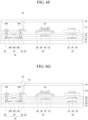
FIG. 2 is a sectional view illustrating another exemplary substrate for a display device according to another embodiment. -
FIG. 3 is a block diagram illustrating a display device that includes the substrate for a display device according to an embodiment. -
FIG. 4 is a sectional view illustrating an organic light-emitting diode display device that includes first and second thin-film transistors and a storage capacitor shown inFIG. 1 according to an embodiment. -
FIG. 5 is a plan view illustrating the storage capacitor shown inFIG. 4 according to an embodiment. -
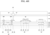
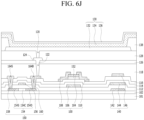
FIGs. 6A to 6J are sectional views for explaining a method of manufacturing the organic light-emitting display device shown inFIG. 4 according to an embodiment. - Reference will now be made in detail to the preferred embodiments, examples of which are illustrated in the accompanying drawings. Wherever possible, the same reference numbers will be used throughout the drawings to refer to like parts.
-
FIG. 1 is a sectional view illustrating a substrate for a display device according to an embodiment. - A substrate for a display device shown in
FIG. 1 includes first and second thin-film transistors storage capacitor 140. - The first thin-
film transistor 100 having a bottom gate configuration includes afirst gate electrode 106, anoxide semiconductor layer 104, afirst source electrode 108, and afirst drain electrode 110. - The
first gate electrode 106, as shown inFIG. 1 , is formed on a firstgate insulation film 112, and may overlap theoxide semiconductor layer 104 with first and secondinterlayer insulation films gate insulation film 152 interposed therebetween. In this case, thefirst gate electrode 106 is disposed on the firstgate insulation film 112, on which asecond gate electrode 156 is also disposed, and is formed of the same material as thesecond gate electrode 156. Accordingly, the first andsecond gate electrodes - The
oxide semiconductor layer 104 is formed on the secondgate insulation film 152 so as to overlap thefirst gate electrode 106, thereby forming a channel between thefirst source electrode 108 and thefirst drain electrode 110. Theoxide semiconductor layer 104 is formed of oxide including at least one metal selected from among Zn, Cd, Ga, In, Sn, Hf, and Zr. Since the first thin-film transistor 100 including thisoxide semiconductor layer 104 has advantages of higher electron mobility and lower off-current than the second thin-film transistor 150 including apolycrystalline semiconductor layer 154, it is suitable for application to a switching thin-film transistor, in which an On-time period is short but an Off-time period is long. Theoxide semiconductor layer 104 may be disposed above thefirst gate electrode 106 so as to effectively ensure the stability of the device. - The second
gate insulation film 152, which has the same shape as theoxide semiconductor layer 104, is formed between theoxide semiconductor layer 104 and at least a first part of the secondinterlayer insulation film 116. The secondgate insulation film 152 may contact the secondinterlayer insulation film 116. The secondgate insulation film 152 is formed of a material having a selective etch ratio different from that of the firstgate insulation film 112 and the first and secondinterlayer insulation films gate insulation film 152 is formed of SiOx, which is an oxide film, and the firstgate insulation film 112 and the first and secondinterlayer insulation films interlayer insulation film 116, which is exposed during a dry-etching process for forming the secondgate insulation film 152 and theoxide semiconductor layer 104, from being damaged by a dry-etching gas used for the dry-etching process. Further, it is possible to prevent the secondgate insulation film 152 and theoxide semiconductor layer 104, which are exposed during a dry-etching process for forming source and draincontact holes gate insulation film 112 and the first and secondinterlayer insulation films - The second
gate insulation film 152 is an inorganic insulation film formed of, for example, silicon oxide (SiOx), which has lower hydrogen particle content than the firstgate insulation film 112. Accordingly, it is possible to prevent hydrogen contained in the firstgate insulation film 112 and hydrogen contained in thepolycrystalline semiconductor layer 154 from being diffused to theoxide semiconductor layer 104 during a heat treatment process performed on theoxide semiconductor layer 104. - Each of the
first source electrode 108 and thefirst drain electrode 110 may be a single layer or multiple layers disposed on the secondinterlayer insulation film 116 and formed of any one selected from among molybdenum (Mo), aluminum (Al), chrome (Cr), gold (Au), titanium (Ti), nickel (Ni), neodymium (Nd), and copper (Cu), or an alloy thereof. However, the embodiment is not limited thereto. Thefirst source electrode 108 and thefirst drain electrode 110 are formed to face each other with the channel of theoxide semiconductor layer 104 interposed therebetween. Meanwhile, an etch stopper (not shown) may be formed on theoxide semiconductor layer 104 that is exposed between thefirst source electrode 108 and thefirst drain electrode 110. The etch stopper protects theoxide semiconductor layer 104, exposed between thefirst source electrode 108 and thefirst drain electrode 110, from oxygen and moisture, thereby preventing damage to theoxide semiconductor layer 104. Thefirst source electrode 108 and thefirst drain electrode 110 may contact side surfaces of the secondgate insulation film 152 that are exposed through the dry-etching process. - The second thin-
film transistor 150 having a top-gate configuration is disposed on asubstrate 101 so as to be spaced apart from the first thin-film transistor 100. The second thin-film transistor 150 includes apolycrystalline semiconductor layer 154, asecond gate electrode 156, asecond source electrode 158, and asecond drain electrode 160. - The
polycrystalline semiconductor layer 154 is formed on abuffer layer 102 that covers thesubstrate 101. Thepolycrystalline semiconductor layer 154 includes achannel region 154C, asource region 154S, and adrain region 154D. Thechannel region 154C overlaps thesecond gate electrode 156 with the firstgate insulation film 112 interposed therebetween, and forms a channel between thesecond source electrode 158 and thesecond drain electrode 160. Thesource region 154S is electrically connected to thesecond source electrode 158 through asource contact hole 164S. Thedrain region 154D is electrically connected to thesecond drain electrode 160 through adrain contact hole 164D. Since thepolycrystalline semiconductor layer 154 has high mobility, low power consumption, and high reliability, it is suitable for applications as a gate-driving unit for driving gate lines and/or to a multiplexer (MUX). - The
second gate electrode 156 overlaps thechannel region 154C of the polycrystalline semiconductor layer with the firstgate insulation film 112 interposed therebetween. Thesecond gate electrode 156 has a smaller line width than thefirst gate electrode 106 and theintermediate storage electrode 144. Thesecond gate electrode 156 may be a single layer or multiple layers formed of the same material as thefirst gate electrode 106, e.g. any one selected from among molybdenum (Mo), aluminum (Al), chrome (Cr), gold (Au), titanium (Ti), nickel (Ni), neodymium (Nd), and copper (Cu), or an alloy thereof. However, the embodiments are not limited thereto. The firstgate insulation film 112 is positioned on thepolycrystalline semiconductor layer 154, and is an inorganic insulation film formed of, for example, silicon nitride (SiNx), which has higher hydrogen particle content than the secondgate insulation film 152. The hydrogen particles contained in the firstgate insulation film 112 are diffused to thepolycrystalline semiconductor layer 154 during a hydrogenation process, thereby enabling pores in thepolycrystalline semiconductor layer 154 to be filled with hydrogen. Accordingly, thepolycrystalline semiconductor layer 154 is stabilized, thus preventing deterioration of the properties of the second thin-film transistor 150. - The
second source electrode 158 is connected to thesource region 154S of thepolycrystalline semiconductor layer 154 through thesource contact hole 164S that penetrates the firstgate insulation film 112 and the first and secondinterlayer insulation films - The
second drain electrode 160 faces thesecond source electrode 158, and is connected to thedrain region 154D of thepolycrystalline semiconductor layer 154 through thedrain contact hole 164D that penetrates the firstgate insulation film 112 and the first and secondinterlayer insulation films second source electrode 158 is in the same layer and is formed of the same material as thefirst source electrode 108, and since thesecond drain electrode 160 is in the same layer and is formed of the same material as thefirst drain electrode 110, the first andsecond source electrodes second drain electrodes - After the activation and hydrogenation processes of the
polycrystalline semiconductor layer 154 of the second thin-film transistor 150, theoxide semiconductor layer 104 of the first thin-film transistor 100 is formed. That is, theoxide semiconductor layer 104 is disposed above thepolycrystalline semiconductor layer 154. Accordingly, theoxide semiconductor layer 104 is not exposed to the high-temperature atmosphere of the activation and hydrogenation processes of thepolycrystalline semiconductor layer 154, thereby preventing damage to theoxide semiconductor layer 104 and therefore improving reliability. - The
storage capacitor 140 includes a first storage capacitor and a second storage capacitor, which are connected in parallel. - The first storage capacitor is formed such that a
lower storage electrode 142 and anintermediate storage electrode 144 overlap each other with the firstgate insulation film 112 interposed therebetween. The second storage capacitor is formed such that theintermediate storage electrode 144 and anupper storage electrode 146 overlap each other with at least one of the first and secondinterlayer insulation films - The
lower storage electrode 142 is disposed on thebuffer film 102, and is positioned in the same layer and is formed of the same material as thepolycrystalline semiconductor layer 154. Theintermediate storage electrode 144 is disposed on the firstgate insulation film 112, and is positioned in the same layer and is formed of the same material as thesecond gate electrode 156. Theupper storage electrode 146 is disposed on the secondinterlayer insulation film 116, and is positioned in the same layer and is formed of the same material as the source and drainelectrodes gate insulation film 112 and the first and secondinterlayer insulation films gate insulation film 112 and the first and secondinterlayer insulation films intermediate storage electrode 144 overlaps thelower storage electrode 142, with the firstgate insulation film 112, which is formed of SiNx having a relatively high dielectric constant, interposed therebetween, the capacity of the first storage capacitor is increased in proportion to the dielectric constant. Similarly, since theupper storage electrode 146 overlaps theintermediate storage electrode 144 with the first and secondinterlayer insulation films interlayer insulation film upper storage electrode 146 and theintermediate storage electrode 144. The secondgate insulation film 152 over theintermediate storage electrode 144 is eliminated through etching process, and thus theupper storage electrode 146 is placed directly on the secondinterlayer insulation film 116. Theupper storage electrode 146 does not contact the secondgate insulation film 152, but contacts the secondinterlayer insulation film 116. On the other hand, in order to further increase the capacity of the second storage capacitor, as shown inFIG. 2 , the secondinterlayer insulation film 116 may be eliminated, and only the firstinterlayer insulation film 114, which is formed of SiNx, may be interposed between theupper storage electrode 146 and theintermediate storage electrode 144. - The substrate for a display device having the above construction according to the present disclosure is applicable to the display device shown in
FIG. 3 . - The display device shown in
FIG. 3 includes adisplay panel 180, a gate-drivingunit 182 for driving gate lines GL of thedisplay panel 180, and a data-drivingunit 184 for driving data lines DL of thedisplay panel 180. - The
display panel 180 includes a display area AA and a non-display area NA surrounding the display area AA. - In the display area AA of the
display panel 180, pixels are located at intersecting portions between the gate lines GL and the data lines DL. The pixels are arranged in a matrix form. Each of the pixels includes thestorage capacitor 140 and at least one of the first thin-film transistor 100 and the second thin-film transistor 150. - The gate-driving
unit 182 is disposed in the non-display area NA. The gate-drivingunit 182 is configured using the second thin-film transistor 150 including thepolycrystalline semiconductor layer 154. The second thin-film transistor 150 of the gate-drivingunit 182 is formed simultaneously with the first and second thin-film transistors - A
multiplexer 186 may be disposed between the data-drivingunit 184 and the data lines DL. Themultiplexer 186 distributes data voltage from the data-drivingunit 184 to the data lines DL in a temporally divided manner, thereby reducing the number of output channels of the data-drivingunit 184 and consequently reducing the number of data driving integrated circuits that compose the data-drivingunit 184. Themultiplexer 186 is configured using the second thin-film transistor 150 including thepolycrystalline semiconductor layer 154. The second thin-film transistor 150 of themultiplexer 186 may be directly formed on thesubstrate 101 for a display device together with the second thin-film transistor 150 of the gate-drivingunit 182 and the first and second thin-film transistors - The above-described display device is applicable to a display device that requires a thin-film transistor, e.g. the organic light-emitting display device shown in
FIG. 4 or a liquid crystal display device. - The organic light-emitting display device shown in
FIG. 4 includes first and second thin-film transistors diode 130 connected to the second thin-film transistor 150, and astorage capacitor 140. - The first thin-
film transistor 100 including anoxide semiconductor layer 104 is applied to a switching transistor of each pixel located in the display area AA, and the second thin-film transistor 150 including apolycrystalline semiconductor layer 154 is applied to a driving transistor of each pixel located in the display area AA. Alternatively, the first thin-film transistor 100 including theoxide semiconductor layer 104 may be applied to a switching transistor for switching data voltage input to each pixel located in the display area AA and to a driving transistor connected to each light-emittingdiode 130. - The second thin-
film transistor 150 including thepolycrystalline semiconductor layer 154 is applied to a transistor of a driving circuit of at least one of the gate-drivingunit 182 located in the non-display area NA and themultiplexer 186. - The
storage capacitor 140 includes alower storage electrode 142, which is disposed on abuffer film 102, and anintermediate storage electrode 144, which overlaps thelower storage electrode 142 with a firstgate insulation film 112 interposed therebetween. Thelower storage electrode 142 is positioned in the same layer and is formed of the same material as thepolycrystalline semiconductor layer 154, and theintermediate storage electrode 144 is positioned in the same layer and is formed of the same material as asecond gate electrode 156. As shown inFIG. 5 , theintermediate storage electrode 144 is connected to adrain electrode 110 of any one of the switching transistor and the driving transistor through a firststorage contact hole 148a, and thelower storage electrode 142 and theupper storage electrode 146 are connected to adrain electrode 160 of the remaining one of the switching transistor and the driving transistor through a secondstorage contact hole 148b. - The light-emitting
diode 130 is a light-emitting device, and includes ananode 132, which is connected to thesecond drain electrode 160 of the second thin-film transistor 150, at least one light-emittingstack 134, which is formed on theanode 132, and acathode 136, which is formed on the light-emittingstack 134. - The
anode 132 is connected to apixel connection electrode 124, which is exposed through a secondpixel contact hole 120 that penetrates aplanarization layer 128. Thepixel connection electrode 124 is connected to thesecond drain electrode 160, which is exposed through a firstpixel contact hole 122 that penetrates first and secondprotective films anode 132 is formed in a multilayer structure including a transparent conductive film and an opaque conductive film having high reflection efficiency. The transparent conductive film is formed of a material having a relatively high work function, e.g. indium tin oxide (ITO) or indium zinc oxide (IZO), and the opaque conductive film is formed in a single-layer or multilayer structure including any one selected from among Al, Ag, Cu, Pb, Mo, and Ti or an alloy thereof. For example, theanode 132 may be formed in a structure such that a transparent conductive film, an opaque conductive film and a transparent conductive film are sequentially stacked, or such that a transparent conductive film and an opaque conductive film are sequentially stacked. Theanode 132 is disposed on theplanarization layer 128 so as to overlap a circuit area, in which the switching and drivingtransistors storage capacitor 140 are disposed, as well as a light-emitting area defined by abank 138, thereby increasing a light-emitting area. - The light-emitting
stack 134 is formed by stacking, on theanode 132, a hole-related layer, an organic light-emitting layer, and an electron-related layer, either in that order or in the reverse order. In addition, the light-emittingstack 134 may include first and second light-emitting stacks, which are opposite each other with a charge generation layer interposed therebetween. In this case, an organic light-emitting layer of any one of the first and second light-emitting stacks generates blue light, and an organic light-emitting layer of the remaining one of the first and second light-emitting stacks generates yellow-green light, with the result that white light is generated via the first and second light-emitting stacks. The white light generated by the light-emittingstack 134 is introduced into a color filter (not shown) disposed on the light-emittingstack 134, and consequently a color image is realized. Alternatively, it may be possible to realize a color image in a way such that each light-emittingstack 134 generates colored light corresponding to each sub-pixel without a separate color filter. That is, a light-emittingstack 134 of a red (R) sub-pixel may generate red light, a light-emittingstack 134 of a green (G) sub-pixel may generate green light, and a light-emittingstack 134 of a blue (B) sub-pixel may generate blue light. - The
bank 138 may be formed so as to expose theanode 132. Thebank 138 may be formed of an opaque material (e.g. a black material) in order to prevent optical interference between neighboring sub-pixels. In this case, thebank 138 includes a light-shielding material including at least one selected from among a color pigment, organic black and carbon materials. - The
cathode 136 is formed on the upper surface and the side surface of the light-emittingstack 134 so as to be opposite theanode 132 with the light-emittingstack 134 interposed therebetween. In the case in which thecathode 136 is applied to a top-emission-type organic light-emitting display device, thecathode 136 is a transparent conductive film formed of, for example, indium tin oxide (ITO) or indium zinc oxide (IZO). - As described above, the first thin-
film transistor 100 including theoxide semiconductor layer 104 is applied to a switching element of each pixel. The first thin-film transistor 100 including theoxide semiconductor layer 104 has lower off-current than the second thin-film transistor 150 including thepolycrystalline semiconductor layer 154. Accordingly, the present disclosure may operate in a low-speed driving mode to lower a frame frequency for a still image or an image having a slow data update interval, thereby reducing power consumption. In addition, theoxide semiconductor layer 104 of the first thin-film transistor 100 has excellent saturation characteristics and therefore facilitates low-voltage operation. - Further, the second thin-
film transistor 150 including thepolycrystalline semiconductor layer 154 is applied to a driving element of each pixel and a driving element of a driving circuit. Since thepolycrystalline semiconductor layer 154 has higher mobility (100 cm2/Vs or more), lower power consumption and higher reliability than theoxide semiconductor layer 104, it is capable of being applied to the gate-drivingunit 182 and/or the multiplexer (MUX) 186. -
FIGs. 6A to 6J are sectional views for explaining a method of manufacturing the organic light-emitting display device shown inFIG. 4 . - Referring to
FIG. 6A , thebuffer layer 102 is formed on thesubstrate 101, and thepolycrystalline semiconductor layer 154 and thelower storage electrode 142 are formed on thebuffer layer 102. - Specifically, an inorganic insulation material, such as SiOx or SiNx, is deposited on the entire surface of the
substrate 101, thereby forming thebuffer layer 102 having a single-layer or multilayer structure. Subsequently, an amorphous silicon thin film is formed on thesubstrate 101, on which thebuffer layer 102 has been formed, using a low-pressure chemical vapor deposition (LPCVD) or plasma-enhanced chemical vapor deposition (PECVD) method. Subsequently, a polycrystalline silicon thin film is formed by crystallizing the amorphous silicon thin film. Subsequently, thepolycrystalline semiconductor layer 154 and thelower storage electrode 142 are formed by patterning the polycrystalline silicon thin film through a photolithography process using a first mask and an etching process. Subsequently, thelower storage electrode 142, excluding thepolycrystalline semiconductor layer 154, is selectively doped with impurities through a photolithography process using a second mask, thereby forming thelower storage electrode 142 having conductivity. - Referring to
FIG. 6B , the firstgate insulation film 112 is formed on thesubstrate 101, on which thepolycrystalline semiconductor layer 154 and thelower storage electrode 142 have been formed, and the first andsecond gate electrodes intermediate storage electrode 144 are formed on the firstgate insulation film 112. - Specifically, an inorganic insulation material such as SiOx is deposited on the entire surface of the
substrate 101, on which thepolycrystalline semiconductor layer 154 and thelower storage electrode 142 have been formed, thereby forming the firstgate insulation film 112. Subsequently, a first conductive layer is deposited on the entire surface of the firstgate insulation film 112, and the first conductive layer is patterned through a photolithography process using a third mask and an etching process, thereby forming the first andsecond gate electrodes intermediate storage electrode 144. - Referring to
FIG. 6C , the first and secondinterlayer insulation films substrate 101, on which the first andsecond gate electrodes intermediate storage electrode 144 have been formed, and the secondgate insulation film 152 and theoxide semiconductor layer 104 are formed on the secondinterlayer insulation film 116 in the same pattern. - Specifically, an inorganic insulation material such as SiNx is deposited on the entire surface of the substrate, on which the first and
second gate electrodes intermediate storage electrode 144 have been formed, thereby forming the first and secondinterlayer insulation films gate insulation film 152, which are formed of an inorganic insulation material such as SiOx, and theoxide semiconductor layer 104, are deposited on the entire surface of the secondinterlayer insulation film 116, and are patterned at the same time through a photolithography process using a fourth mask and an etching process, thereby forming the secondgate insulation film 152 and theoxide semiconductor layer 104 in the same pattern. For example, an insulation film may be deposited on the substrate, and an oxide semiconductor layer may be deposited on the insulation film. The oxide semiconductor layer may be patterned using the fourth mask to form theoxide semiconductor layer 104, and the insulation film may be patterned using the same fourth mask to form the secondgate insulation film 152. - Referring to
FIG. 6D , the source and draincontact holes substrate 101, on which the secondgate insulation film 152 and theoxide semiconductor layer 104 have been formed. - Specifically, the first
gate insulation film 112 and the first and secondinterlayer insulation films substrate 101, on which the secondgate insulation film 152 and theoxide semiconductor layer 104 have been formed, are patterned through a photolithography process using a fifth mask and an etching process, thereby forming the source and draincontact holes - Referring to
FIG. 6E , the first andsecond source electrodes second drain electrodes upper storage electrode 146 are formed on thesubstrate 101, on which the source and draincontact holes - Specifically, a second conductive layer is deposited on the entire surface of the
substrate 101, on which the source and draincontact holes second source electrodes second drain electrodes upper storage electrode 146. Due to patterning of the secondgate insulation film 152, theupper storage electrode 146 does not contact the secondgate insulation film 152, but may instead contact the secondinterlayer insulation film 116. - Referring to
FIG. 6F , the first and secondprotective films pixel contact hole 122 are formed on thesubstrate 101, on which the first andsecond source electrodes second drain electrodes upper storage electrode 146 have been formed. - Specifically, the first and second
protective films substrate 101, on which the first andsecond source electrodes second drain electrodes upper storage electrode 146 have been formed, through a deposition process. Here, the first and secondprotective films protective films pixel contact hole 122. - Referring to
FIG. 6G , thepixel connection electrode 124 is formed on thesubstrate 101, on which the first and secondprotective films pixel contact hole 122 have been formed. - Specifically, a third conductive layer is deposited on the entire surface of the
substrate 101, on which the first and secondprotective films pixel contact hole 122 have been formed, and is patterned through a photolithography process using an eighth mask and an etching process, thereby forming thepixel connection electrode 124. - Referring to
FIG. 6H , theplanarization layer 128 having the secondpixel contact hole 120 is formed on thesubstrate 101, on which thepixel connection electrode 124 has been formed. - Specifically, an organic insulation material such as acrylic resin is deposited on the entire surface of the
substrate 101, on which thepixel connection electrode 124 has been formed, thereby forming theplanarization layer 128. Subsequently, theplanarization layer 128 is patterned through a photolithography process using a ninth mask and an etching process, thereby forming the secondpixel contact hole 120. - Referring to
FIG. 6I , theanode 132 is formed on thesubstrate 101, on which theplanarization layer 128 having the secondpixel contact hole 120 has been formed. - Specifically, a fourth conductive layer is deposited on the entire surface of the
substrate 101, on which theplanarization layer 128 having the secondpixel contact hole 120 has been formed. The fourth conductive layer includes a transparent conductive film and an opaque conductive film. Subsequently, the fourth conductive layer is patterned through a photolithography process and an etching process, thereby forming theanode 132. - Referring to
FIG. 6J , thebank 138, the organic light-emittingstack 134 and thecathode 136 are sequentially formed on thesubstrate 101, on which theanode 132 has been formed. - Specifically, a photosensitive film is coated on the entire surface of the
substrate 101, on which theanode 132 has been formed, and is patterned through a photolithography process, thereby forming thebank 138. Subsequently, the light-emittingstack 134 and thecathode 136 are sequentially formed in the display area AA, but not the non-display area NA, through a deposition process using a shadow mask. - As such, according to the present disclosure, the
intermediate storage electrode 144 and thegate electrodes upper storage electrode 146 and the source and drainelectrodes - As is apparent from the above description, lower power consumption and low-voltage operation may be achieved by applying a thin-film transistor including an oxide semiconductor layer to a thin-film transistor positioned in a display area. In addition, the number of driving integrated circuits may be reduced and a bezel area may be reduced by applying a thin-film transistor including a polycrystalline semiconductor layer to a gate-driving unit positioned in a non-display area and a multiplexer. In addition, one of at least two storage electrodes is formed simultaneously with a gate electrode through the same single mask process, and another one of the at least two storage electrodes is formed simultaneously with source and drain electrodes through the same single mask process. Accordingly, an organic light-emitting display device according to the present disclosure is capable of reducing one or more mask processes, as compared to the prior art, thereby simplifying the structure and the manufacturing process thereof and improving productivity.
- It will be apparent to those skilled in the art that various modifications and variations can be made in the present disclosure without departing from the scope of the appended claims. Thus, it is intended that the present disclosure covers modifications and variations within the scope of the appended claims and their equivalents. The disclosure comprises the following items:
- 1. A display device comprising:
- a substrate (101);
- a pixel on the substrate (101), the pixel including:
- a first thin-film transistor (TFT) (100) on the substrate (101), the first TFT (100) including:
- a first gate electrode (106),
- at least a first part of an interlayer insulation film (114) on the first gate electrode (106),
- a first gate insulation film (152) on the first part of the interlayer insulation film (114), and
- a first active layer (104) formed of oxide semiconductor (104) on the first gate insulation film (152);
- a storage capacitor (140) on the substrate (101), the storage capacitor (140) including:
- a first storage electrode (144),
- at least a second part of the interlayer insulation film (114) on the first storage electrode (144), and
- a second storage electrode (146) on the second part of the interlayer insulation film (114),
- wherein the second storage electrode (146) is physically separated from the first gate insulation film (152); and
- a light-emitting device (130) electrically connected to the storage capacitor (140).
- a first thin-film transistor (TFT) (100) on the substrate (101), the first TFT (100) including:
- 2. The display device of item 1, wherein the first gate insulation film (152) and the second storage electrode (146) contact the interlayer insulation film (114).
- 3. The display device of item 1, wherein the first storage electrode (144) is in a same layer as the first gate electrode (106).
- 4. The display device of item 1, wherein the interlayer insulation film (114) is formed of silicon nitride (SiNx) and the first gate insulation film (152) is formed of silicon oxide (SiOx).
- 5. The display device of item 1, wherein the first TFT (106) further includes a first source electrode and a first drain electrode (110) electrically connected to the first active layer (104), and wherein the second storage electrode (146) is in a same layer as the first source electrode (108) and the first drain electrode (110) .
- 6. The display device of item 1, wherein the first TFT (100) further includes a first source electrode (108) and a first drain electrode (110) electrically connected to the first active layer (104), and wherein the first source electrode (108) or the first drain electrode (110) contacts a side surface of the first gate insulation film (152), optionally wherein the first source electrode (108) or the first drain electrode (110) contacts a side surface of the first active layer (104) .
- 7. The display device of item 1, further comprising a second TFT (150) on the substrate (101), the second TFT (150) including:
- a second active layer (154) formed of polycrystalline silicon;
- at least a first part of a second gate insulation film (112) on the second active layer (154); and
- a second gate electrode (156) on the first part of the second gate insulation film (112),
- wherein the second gate electrode (156) is in a same layer as the first gate electrode (106),
- optionally wherein the first active layer (104) is disposed above the second active layer (154).
- 8. The display device of item 7, further comprising a third TFT disposed in a non-display area (NA) of the substrate (101), the third TFT including a third active layer formed of poly-Si, optionally further comprising:
- a gate-driving unit (182) disposed in the non-display area (NA) to drive gate lines (GL) in a display area (AA) of the substrate (101);
- a data-driving unit (184) disposed in the non-display area (NA) for driving data lines (DL) in the display area (AA); and
- a multiplexer (186) for distributing data voltage from the data-driving unit (184) to the data lines (DL),
- wherein the third TFT is included in at least one of the multiplexer (186) and the gate-driving unit (182).
- 9. The display device of item 7, wherein the first TFT (100) is a switching TFT of the pixel, and wherein the second TFT (150) is a driving TFT of the pixel,
- optionally wherein the light-emitting device (130) comprises an anode electrode (132), a light-emitting stack (134), and a cathode electrode (136), wherein the anode electrode (132) overlaps with the first TFT (100), the second TFT (150), and the storage capacitor (140),
- optionally wherein the second gate electrode (156) has a smaller line width than the first gate electrode (106) and the first storage electrode (144).
- 10. The display device of item 7, wherein the storage capacitor (140) further includes a third storage electrode (142) on the substrate (101), and at least a second part of the second gate insulation film (112) on the third storage electrode, optionally wherein the third storage electrode (142) is in a same layer as the second active layer (154).
- 11. The display device of item 1, wherein the light-emitting device (130) comprises an anode electrode (132), a light-emitting stack (134), and a cathode electrode (136), wherein the second TFT (150) includes a second drain electrode (160) electrically connected to the second active layer (154), and wherein the display device further comprises a connection electrode (124) electrically connected to the second drain electrode (160) and the anode electrode (132).
- 12. The display device of item 1, wherein the light-emitting device (130) comprises an anode electrode (132), a light-emitting stack (134), and a cathode electrode (136), and wherein the anode electrode (132) includes a transparent conductive film and an opaque conductive film.
- 13. The display device of item 1, wherein the light-emitting device (130) comprises an anode electrode (132), a light-emitting stack (134), and a cathode electrode (136), wherein the display device further comprises a bank layer (138) on at least a part of the anode electrode (132), and wherein the bank layer (138) includes a light-shielding material selected from at least one among a color pigment and organic black and carbon materials.
- 14. The display device of item 1, further comprising a color filter on the light-emitting device (130).
- 15. A method of manufacturing the display device including a substrate (101) and a pixel on the substrate (101) according to any one of items 1-14, the method comprising:
- patterning a first conductive layer using a first mask to form a first gate electrode (106) of a first thin-film transistor (TFT) (100) and a first storage electrode (144) of a storage capacitor (140) on the substrate (101),
- forming an interlayer insulation film (114) on the first gate electrode (106) and the first storage electrode (144) using a second mask to form a first gate insulation film (112) on at least a first part of the interlayer insulation film (114),
- patterning an oxide semiconductor layer (104) using the second mask to form a first active layer (104) of the first TFT (100) on the first gate insulation film (112), and
- forming a second storage electrode (146) of the storage capacitor (140) on at least a second part of the interlayer insulation film (114), wherein the second storage electrode (146) does not contact the first gate insulation film (112).
Claims (15)
- A display device comprising:a substrate (101);a pixel on the substrate (101), the pixel including:a first thin-film transistor "TFT" (100) on the substrate (101), the first TFT (100) including an oxide semiconductor layer (104);a second TFT (150) on the substrate (101), the second TFT (150) being spaced apart from the first TFT (100) and including a polycrystalline silicon semiconductor layer (154);a storage capacitor (140) on the substrate (101), the storage capacitor (140) including first and second storage electrodes (144, 146) ; anda light-emitting device (130) electrically connected to the storage capacitor (140), the light-emitting device (130) including an anode electrode (132), a light-emitting stack (134), and a cathode electrode (136),wherein the display device further comprises:a first protective film (118);a second protective film (126);a planarization layer (128); anda pixel connection electrode (124),wherein the pixel connection electrode (124) is connected to a drain electrode (160) of the second TFT (150), which is exposed through a first pixel contact hole (122) that penetrates the first and second protective films (118, 126), and the anode electrode (132) is connected to the pixel connection electrode (124), which is exposed through a second pixel contact hole (120) that penetrates the planarization layer (128).
- The display device of claim 1, wherein a first gate insulation film (152) and the second storage electrode (146) contact an interlayer insulation film (114) on a first gate electrode (106) of the first TFT (100).
- The display device of claim 1, wherein the first storage electrode (144) is in a same layer as a first gate electrode (106) of the first TFT (100).
- The display device of claim 1, wherein an interlayer insulation film (114) is formed of silicon nitride (SiNx) and a first gate insulation film (152) is formed of silicon oxide (SiOx).
- The display device of claim 1, wherein a second gate electrode (156) of the second TFT (150) is in the same layer as the first storage electrode (144).
- The display device of claim 1, wherein the second TFT (150) includes:at least a first part of a second gate insulation film (112) on the polycrystalline semiconductor layer (154); anda second gate electrode (156) of the second TFT (150) on the first part of the second gate insulation film (112).
- The display device of claim 6, further comprising a third TFT disposed in a non-display area (NA) of the substrate (101), the third TFT including a third active layer formed of poly-Si, optionally further comprising:a gate-driving unit (182) disposed in the non-display area (NA) to drive gate lines (GL) in a display area (AA) of the substrate (101); anda data-driving unit (184) disposed in the non-display area (NA) for driving data lines (DL) in the display area (AA),wherein the third TFT is included in the gate-driving unit (182).
- The display device of claim 6, wherein the first TFT (100) is a switching TFT of the pixel, and wherein the second TFT (150) is a driving TFT of the pixel, optionally wherein the anode electrode (132) overlaps with the first TFT (100), the second TFT (150), and the storage capacitor (140).
- The display device of claim 1, wherein the second TFT (150) is electrically connected to the polycrystalline semiconductor layer (154).
- The display device of claim 1, wherein the first TFT (106) further includes a first source electrode (108) and a first drain electrode (110) electrically connected to the oxide semiconductor layer (104), and wherein the second TFT (150) further includes a second source electrode (158), and
wherein the first source electrode (108), the first drain electrode (110), the second source electrode (158) and the second drain electrode (160) are in the same layer. - The display device of claim 1, wherein the oxide semiconductor layer (104) is disposed above the polycrystalline semiconductor layer (154).
- The display device of claim 1, wherein the anode electrode (132) includes a transparent conductive film and an opaque conductive film.
- The display device of claim 1, further comprising a color filter on the light-emitting device (130).
- The display device of claim 1, wherein the first storage electrode (144) is connected to a drain electrode (110, 160) of the first TFT (100) or the second TFT (150).
- The display device of claim 1, wherein the light-emitting stack (134) comprises a hole-related layer, an organic light-emitting layer, and an electron-related layer, optionally wherein the light-emitting stack (134) comprises first and second light-emitting stacks, which are opposite each other with a charge generation layer interposed therebetween.
Applications Claiming Priority (2)
| Application Number | Priority Date | Filing Date | Title |
|---|---|---|---|
| KR1020160174261A KR20180071538A (en) | 2016-12-20 | 2016-12-20 | Substrate for display and display including the same |
| EP17208677.9A EP3340301B1 (en) | 2016-12-20 | 2017-12-19 | Substrate for display device and display device including the same |
Related Parent Applications (1)
| Application Number | Title | Priority Date | Filing Date |
|---|---|---|---|
| EP17208677.9A Division EP3340301B1 (en) | 2016-12-20 | 2017-12-19 | Substrate for display device and display device including the same |
Publications (2)
| Publication Number | Publication Date |
|---|---|
| EP4398301A2 true EP4398301A2 (en) | 2024-07-10 |
| EP4398301A3 EP4398301A3 (en) | 2024-09-25 |
Family
ID=60937551
Family Applications (2)
| Application Number | Title | Priority Date | Filing Date |
|---|---|---|---|
| EP24178116.0A Pending EP4398301A3 (en) | 2016-12-20 | 2017-12-19 | Substrate for display device and display device including the same |
| EP17208677.9A Active EP3340301B1 (en) | 2016-12-20 | 2017-12-19 | Substrate for display device and display device including the same |
Family Applications After (1)
| Application Number | Title | Priority Date | Filing Date |
|---|---|---|---|
| EP17208677.9A Active EP3340301B1 (en) | 2016-12-20 | 2017-12-19 | Substrate for display device and display device including the same |
Country Status (4)
| Country | Link |
|---|---|
| US (2) | US10340320B2 (en) |
| EP (2) | EP4398301A3 (en) |
| KR (1) | KR20180071538A (en) |
| CN (2) | CN108206192B (en) |
Families Citing this family (37)
| Publication number | Priority date | Publication date | Assignee | Title |
|---|---|---|---|---|
| KR102109166B1 (en) * | 2013-01-15 | 2020-05-12 | 삼성디스플레이 주식회사 | Thin film transistor and display substrate having the same |
| KR20180071538A (en) * | 2016-12-20 | 2018-06-28 | 엘지디스플레이 주식회사 | Substrate for display and display including the same |
| KR102873477B1 (en) * | 2016-12-28 | 2025-10-20 | 엘지디스플레이 주식회사 | Substrate for display and display including the same |
| KR102465376B1 (en) * | 2017-06-16 | 2022-11-10 | 삼성디스플레이 주식회사 | Display apparatus and method for manufacturing the same |
| KR102173434B1 (en) * | 2017-12-19 | 2020-11-03 | 엘지디스플레이 주식회사 | Display device |
| CN108288621B (en) * | 2018-03-09 | 2021-01-26 | 京东方科技集团股份有限公司 | Manufacturing method of array substrate, array substrate and display panel |
| US11476314B2 (en) * | 2018-03-29 | 2022-10-18 | Sharp Kabushiki Kaisha | Display device and production method for display device |
| CN109065590B (en) | 2018-08-09 | 2020-12-04 | 京东方科技集团股份有限公司 | Organic light-emitting display substrate and method of making the same, and organic light-emitting display device |
| KR102469187B1 (en) * | 2018-09-04 | 2022-11-21 | 삼성디스플레이 주식회사 | Display device and method for manufacturing the same |
| US10910413B2 (en) * | 2018-10-10 | 2021-02-02 | HKC Corporation Limited | Method of manufacturing array substrate and array substrate |
| KR102711213B1 (en) * | 2018-10-15 | 2024-09-27 | 엘지디스플레이 주식회사 | Display panel and display device |
| JP6753450B2 (en) * | 2018-11-12 | 2020-09-09 | セイコーエプソン株式会社 | Substrates for electro-optical devices, electro-optic devices, electronic devices |
| KR102701984B1 (en) | 2018-12-26 | 2024-09-02 | 엘지디스플레이 주식회사 | Display apparatus comprising different types of thin film transistors and mehthod for manufacturing the same |
| KR102690931B1 (en) | 2019-01-17 | 2024-08-01 | 삼성디스플레이 주식회사 | Display device including the same, and method for manufacturing the same |
| WO2020210946A1 (en) * | 2019-04-15 | 2020-10-22 | Boe Technology Group Co., Ltd. | Method of fabricating array substrate, array substrate, and display apparatus |
| WO2020231398A1 (en) * | 2019-05-13 | 2020-11-19 | Hewlett-Packard Development Company, L.P. | Thin-film transistors |
| US11482586B2 (en) * | 2019-07-31 | 2022-10-25 | Beijing Boe Technology Development Co., Ltd. | Array substrate having groups of transistors with source and drain electrode indifferent layers |
| KR102812018B1 (en) * | 2019-08-26 | 2025-05-23 | 엘지디스플레이 주식회사 | Display Panel and Head Mounted Display Device Having the Same Therein |
| CN110556386A (en) * | 2019-09-05 | 2019-12-10 | 京东方科技集团股份有限公司 | Drive backplane, preparation method thereof, and display panel |
| KR102853446B1 (en) * | 2019-10-11 | 2025-09-02 | 삼성디스플레이 주식회사 | Display device and method for manufacturing the same |
| KR102825654B1 (en) * | 2019-12-24 | 2025-06-26 | 엘지디스플레이 주식회사 | Display device |
| CN111834400B (en) * | 2020-02-26 | 2021-10-12 | 昆山国显光电有限公司 | Display panel, manufacturing method thereof and display device |
| KR102867626B1 (en) * | 2020-03-18 | 2025-10-02 | 삼성디스플레이 주식회사 | Display device and method of fabricating for display device |
| CN111384070B (en) * | 2020-03-25 | 2023-05-19 | 京东方科技集团股份有限公司 | Pixel structure, array substrate, display device and manufacturing method |
| US20220140048A1 (en) * | 2020-03-31 | 2022-05-05 | Boe Technology Group Co., Ltd. | Display panel, method for preparing the same, and display device |
| CN111933681A (en) * | 2020-09-07 | 2020-11-13 | 深圳市华星光电半导体显示技术有限公司 | Top-emission AMOLED display panel, manufacturing method and display device |
| US12225771B2 (en) * | 2020-09-10 | 2025-02-11 | Samsung Display Co., Ltd. | Display device and method of manufacturing the same |
| CN112670247B (en) * | 2020-12-23 | 2024-02-02 | 武汉天马微电子有限公司 | Preparation method of display panel, display panel and display device |
| KR102804064B1 (en) * | 2020-12-29 | 2025-05-09 | 엘지디스플레이 주식회사 | Display panel and manufacturing method thereof |
| CN119997606A (en) * | 2020-12-30 | 2025-05-13 | 厦门天马微电子有限公司 | Display panel and display device |
| KR20220097675A (en) | 2020-12-30 | 2022-07-08 | 삼성디스플레이 주식회사 | Display apparatus |
| KR102946901B1 (en) * | 2021-03-26 | 2026-04-01 | 삼성디스플레이 주식회사 | Display apparatus |
| KR20230119822A (en) * | 2022-02-08 | 2023-08-16 | 엘지디스플레이 주식회사 | Organic Light Emitting Diode Display Device and Manufacturing method thereof |
| US20240324372A1 (en) * | 2022-04-19 | 2024-09-26 | Beijing Boe Technology Development Co., Ltd. | Display Substrate and Display Apparatus |
| US20240306445A1 (en) * | 2022-06-30 | 2024-09-12 | Chengdu Boe Optoelectronics Technology Co., Ltd. | Display panel and display device |
| TWI802478B (en) * | 2022-07-27 | 2023-05-11 | 友達光電股份有限公司 | Active component substrate |
| KR20260025965A (en) * | 2024-08-16 | 2026-02-25 | 삼성디스플레이 주식회사 | Display device and manufacturing method of the same |
Family Cites Families (22)
| Publication number | Priority date | Publication date | Assignee | Title |
|---|---|---|---|---|
| EP1020920B1 (en) * | 1999-01-11 | 2010-06-02 | Sel Semiconductor Energy Laboratory Co., Ltd. | Semiconductor device having a driver TFT and a pixel TFT on a common substrate |
| KR100726132B1 (en) * | 2000-10-31 | 2007-06-12 | 엘지.필립스 엘시디 주식회사 | Array substrate for liquid crystal display device and manufacturing method |
| KR101074788B1 (en) * | 2009-01-30 | 2011-10-20 | 삼성모바일디스플레이주식회사 | Flat panel display apparatus and the manufacturing method thereof |
| TWI476917B (en) * | 2009-04-16 | 2015-03-11 | 半導體能源研究所股份有限公司 | Semiconductor device and method of manufacturing same |
| WO2011007675A1 (en) * | 2009-07-17 | 2011-01-20 | Semiconductor Energy Laboratory Co., Ltd. | Semiconductor device and manufacturing method thereof |
| KR101346874B1 (en) | 2010-08-30 | 2014-01-02 | 샤프 가부시키가이샤 | Semiconductor device and process for production thereof |
| KR101781532B1 (en) | 2011-03-14 | 2017-10-24 | 삼성디스플레이 주식회사 | An organic light emitting display device and the manufacturing method thereof |
| TWI453516B (en) | 2011-07-13 | 2014-09-21 | 友達光電股份有限公司 | Pixel structure and its making method |
| KR102072244B1 (en) * | 2011-11-30 | 2020-01-31 | 가부시키가이샤 한도오따이 에네루기 켄큐쇼 | Semiconductor device and method for manufacturing the same |
| KR101901832B1 (en) * | 2011-12-14 | 2018-09-28 | 삼성디스플레이 주식회사 | Organic light emitting display apparatus and method of manufacturing organic light emitting display apparatus |
| US9929276B2 (en) * | 2012-08-10 | 2018-03-27 | Semiconductor Energy Laboratory Co., Ltd. | Semiconductor device and method for manufacturing the same |
| KR102109166B1 (en) * | 2013-01-15 | 2020-05-12 | 삼성디스플레이 주식회사 | Thin film transistor and display substrate having the same |
| KR102077143B1 (en) * | 2013-05-30 | 2020-02-14 | 삼성디스플레이 주식회사 | Organic light emitting display device and manufacturing method of the same |
| US9818765B2 (en) * | 2013-08-26 | 2017-11-14 | Apple Inc. | Displays with silicon and semiconducting oxide thin-film transistors |
| US10325937B2 (en) * | 2014-02-24 | 2019-06-18 | Lg Display Co., Ltd. | Thin film transistor substrate with intermediate insulating layer and display using the same |
| US10083990B2 (en) * | 2014-08-29 | 2018-09-25 | Lg Display Co., Ltd. | Thin film transistor substrate and display device using the same |
| US9543370B2 (en) * | 2014-09-24 | 2017-01-10 | Apple Inc. | Silicon and semiconducting oxide thin-film transistor displays |
| KR102226236B1 (en) * | 2014-10-13 | 2021-03-11 | 엘지디스플레이 주식회사 | Organic light emitting display |
| US10020354B2 (en) * | 2015-04-17 | 2018-07-10 | Apple Inc. | Organic light-emitting diode displays with silicon and semiconducting oxide thin-film transistors |
| CN105929615B (en) * | 2016-06-21 | 2019-05-03 | 武汉华星光电技术有限公司 | A thin film transistor array substrate and a liquid crystal panel |
| US9985082B2 (en) * | 2016-07-06 | 2018-05-29 | Lg Display Co., Ltd. | Organic light emitting display device comprising multi-type thin film transistor and method of manufacturing the same |
| KR20180071538A (en) * | 2016-12-20 | 2018-06-28 | 엘지디스플레이 주식회사 | Substrate for display and display including the same |
-
2016
- 2016-12-20 KR KR1020160174261A patent/KR20180071538A/en active Pending
-
2017
- 2017-11-10 US US15/809,946 patent/US10340320B2/en active Active
- 2017-11-28 CN CN201711215133.0A patent/CN108206192B/en active Active
- 2017-11-28 CN CN202210153249.0A patent/CN114664865B/en active Active
- 2017-12-19 EP EP24178116.0A patent/EP4398301A3/en active Pending
- 2017-12-19 EP EP17208677.9A patent/EP3340301B1/en active Active
-
2019
- 2019-05-10 US US16/409,718 patent/US10714557B2/en active Active
Also Published As
| Publication number | Publication date |
|---|---|
| US20180175127A1 (en) | 2018-06-21 |
| US20190267441A1 (en) | 2019-08-29 |
| US10340320B2 (en) | 2019-07-02 |
| CN114664865A (en) | 2022-06-24 |
| US10714557B2 (en) | 2020-07-14 |
| EP4398301A3 (en) | 2024-09-25 |
| KR20180071538A (en) | 2018-06-28 |
| EP3340301A1 (en) | 2018-06-27 |
| CN108206192A (en) | 2018-06-26 |
| CN108206192B (en) | 2022-03-11 |
| CN114664865B (en) | 2026-03-17 |
| EP3340301B1 (en) | 2024-06-12 |
Similar Documents
| Publication | Publication Date | Title |
|---|---|---|
| US10714557B2 (en) | Substrate for display device and display device including the same | |
| US10692893B2 (en) | Substrate for display device and display device including the same | |
| USRE50892E1 (en) | Display apparatus | |
| US11765937B2 (en) | Display device | |
| US11158700B2 (en) | Display device having multiple buffer layers | |
| US10937816B2 (en) | Switching element, manufacturing method thereof, array substrate and display device | |
| KR102457204B1 (en) | Thin Film Transistor Substrate And Display Using The Same | |
| JP2017120893A (en) | Thin film transistor substrate | |
| KR102468858B1 (en) | Substrate for display and display including the same | |
| KR20120053768A (en) | Organic light emitting display device and method for fabricating the same | |
| KR102585853B1 (en) | Substrate for display and display including the same | |
| KR102220681B1 (en) | Display device having organic light emitting diode source | |
| KR102501143B1 (en) | Manufacturing method of the display device | |
| KR102871406B1 (en) | Display device and method of manufacturing the same | |
| KR20200020327A (en) | Substrate for display and display including the same |
Legal Events
| Date | Code | Title | Description |
|---|---|---|---|
| PUAI | Public reference made under article 153(3) epc to a published international application that has entered the european phase |
Free format text: ORIGINAL CODE: 0009012 |
|
| STAA | Information on the status of an ep patent application or granted ep patent |
Free format text: STATUS: REQUEST FOR EXAMINATION WAS MADE |
|
| 17P | Request for examination filed |
Effective date: 20240525 |
|
| AC | Divisional application: reference to earlier application |
Ref document number: 3340301 Country of ref document: EP Kind code of ref document: P |
|
| AK | Designated contracting states |
Kind code of ref document: A2 Designated state(s): AL AT BE BG CH CY CZ DE DK EE ES FI FR GB GR HR HU IE IS IT LI LT LU LV MC MK MT NL NO PL PT RO RS SE SI SK SM TR |
|
| REG | Reference to a national code |
Ref country code: DE Ref legal event code: R079 Free format text: PREVIOUS MAIN CLASS: H01L0027120000 Ipc: H10K0059121000 |
|
| PUAL | Search report despatched |
Free format text: ORIGINAL CODE: 0009013 |
|
| AK | Designated contracting states |
Kind code of ref document: A3 Designated state(s): AL AT BE BG CH CY CZ DE DK EE ES FI FR GB GR HR HU IE IS IT LI LT LU LV MC MK MT NL NO PL PT RO RS SE SI SK SM TR |
|
| RIC1 | Information provided on ipc code assigned before grant |
Ipc: H01L 27/12 20060101ALI20240821BHEP Ipc: H10K 59/121 20230101AFI20240821BHEP |
|
| RBV | Designated contracting states (corrected) |
Designated state(s): AL AT BE BG CH CY CZ DE DK EE ES FI FR GB GR HR HU IE IS IT LI LT LU LV MC MK MT NL NO PL PT RO RS SE SI SK SM TR |
|
| STAA | Information on the status of an ep patent application or granted ep patent |
Free format text: STATUS: EXAMINATION IS IN PROGRESS |
|
| 17Q | First examination report despatched |
Effective date: 20260312 |