EP4397155B1 - Perowskit-solarzelle - Google Patents
Perowskit-solarzelle Download PDFInfo
- Publication number
- EP4397155B1 EP4397155B1 EP22773476.1A EP22773476A EP4397155B1 EP 4397155 B1 EP4397155 B1 EP 4397155B1 EP 22773476 A EP22773476 A EP 22773476A EP 4397155 B1 EP4397155 B1 EP 4397155B1
- Authority
- EP
- European Patent Office
- Prior art keywords
- perovskite
- solar cell
- electrode layer
- layer
- back electrode
- Prior art date
- Legal status (The legal status is an assumption and is not a legal conclusion. Google has not performed a legal analysis and makes no representation as to the accuracy of the status listed.)
- Active
Links
Images

Classifications
-
- H—ELECTRICITY
- H10—SEMICONDUCTOR DEVICES; ELECTRIC SOLID-STATE DEVICES NOT OTHERWISE PROVIDED FOR
- H10K—ORGANIC ELECTRIC SOLID-STATE DEVICES
- H10K30/00—Organic devices sensitive to infrared radiation, light, electromagnetic radiation of shorter wavelength or corpuscular radiation
- H10K30/30—Organic devices sensitive to infrared radiation, light, electromagnetic radiation of shorter wavelength or corpuscular radiation comprising bulk heterojunctions, e.g. interpenetrating networks of donor and acceptor material domains
-
- H—ELECTRICITY
- H10—SEMICONDUCTOR DEVICES; ELECTRIC SOLID-STATE DEVICES NOT OTHERWISE PROVIDED FOR
- H10K—ORGANIC ELECTRIC SOLID-STATE DEVICES
- H10K30/00—Organic devices sensitive to infrared radiation, light, electromagnetic radiation of shorter wavelength or corpuscular radiation
- H10K30/80—Constructional details
- H10K30/81—Electrodes
-
- H—ELECTRICITY
- H10—SEMICONDUCTOR DEVICES; ELECTRIC SOLID-STATE DEVICES NOT OTHERWISE PROVIDED FOR
- H10K—ORGANIC ELECTRIC SOLID-STATE DEVICES
- H10K30/00—Organic devices sensitive to infrared radiation, light, electromagnetic radiation of shorter wavelength or corpuscular radiation
- H10K30/10—Organic devices sensitive to infrared radiation, light, electromagnetic radiation of shorter wavelength or corpuscular radiation comprising heterojunctions between organic semiconductors and inorganic semiconductors
- H10K30/15—Sensitised wide-bandgap semiconductor devices, e.g. dye-sensitised TiO2
- H10K30/151—Sensitised wide-bandgap semiconductor devices, e.g. dye-sensitised TiO2 the wide bandgap semiconductor comprising titanium oxide, e.g. TiO2
-
- H—ELECTRICITY
- H10—SEMICONDUCTOR DEVICES; ELECTRIC SOLID-STATE DEVICES NOT OTHERWISE PROVIDED FOR
- H10K—ORGANIC ELECTRIC SOLID-STATE DEVICES
- H10K30/00—Organic devices sensitive to infrared radiation, light, electromagnetic radiation of shorter wavelength or corpuscular radiation
- H10K30/30—Organic devices sensitive to infrared radiation, light, electromagnetic radiation of shorter wavelength or corpuscular radiation comprising bulk heterojunctions, e.g. interpenetrating networks of donor and acceptor material domains
- H10K30/353—Organic devices sensitive to infrared radiation, light, electromagnetic radiation of shorter wavelength or corpuscular radiation comprising bulk heterojunctions, e.g. interpenetrating networks of donor and acceptor material domains comprising blocking layers, e.g. exciton blocking layers
-
- H—ELECTRICITY
- H10—SEMICONDUCTOR DEVICES; ELECTRIC SOLID-STATE DEVICES NOT OTHERWISE PROVIDED FOR
- H10K—ORGANIC ELECTRIC SOLID-STATE DEVICES
- H10K30/00—Organic devices sensitive to infrared radiation, light, electromagnetic radiation of shorter wavelength or corpuscular radiation
- H10K30/40—Organic devices sensitive to infrared radiation, light, electromagnetic radiation of shorter wavelength or corpuscular radiation comprising a p-i-n structure, e.g. having a perovskite absorber between p-type and n-type charge transport layers
-
- H—ELECTRICITY
- H10—SEMICONDUCTOR DEVICES; ELECTRIC SOLID-STATE DEVICES NOT OTHERWISE PROVIDED FOR
- H10K—ORGANIC ELECTRIC SOLID-STATE DEVICES
- H10K30/00—Organic devices sensitive to infrared radiation, light, electromagnetic radiation of shorter wavelength or corpuscular radiation
- H10K30/50—Photovoltaic [PV] devices
-
- H—ELECTRICITY
- H10—SEMICONDUCTOR DEVICES; ELECTRIC SOLID-STATE DEVICES NOT OTHERWISE PROVIDED FOR
- H10K—ORGANIC ELECTRIC SOLID-STATE DEVICES
- H10K30/00—Organic devices sensitive to infrared radiation, light, electromagnetic radiation of shorter wavelength or corpuscular radiation
- H10K30/80—Constructional details
- H10K30/84—Layers having high charge carrier mobility
- H10K30/85—Layers having high electron mobility, e.g. electron-transporting layers or hole-blocking layers
-
- H—ELECTRICITY
- H10—SEMICONDUCTOR DEVICES; ELECTRIC SOLID-STATE DEVICES NOT OTHERWISE PROVIDED FOR
- H10K—ORGANIC ELECTRIC SOLID-STATE DEVICES
- H10K30/00—Organic devices sensitive to infrared radiation, light, electromagnetic radiation of shorter wavelength or corpuscular radiation
- H10K30/80—Constructional details
- H10K30/84—Layers having high charge carrier mobility
- H10K30/86—Layers having high hole mobility, e.g. hole-transporting layers or electron-blocking layers
-
- H—ELECTRICITY
- H10—SEMICONDUCTOR DEVICES; ELECTRIC SOLID-STATE DEVICES NOT OTHERWISE PROVIDED FOR
- H10K—ORGANIC ELECTRIC SOLID-STATE DEVICES
- H10K30/00—Organic devices sensitive to infrared radiation, light, electromagnetic radiation of shorter wavelength or corpuscular radiation
- H10K30/80—Constructional details
- H10K30/88—Passivation; Containers; Encapsulations
-
- H—ELECTRICITY
- H10—SEMICONDUCTOR DEVICES; ELECTRIC SOLID-STATE DEVICES NOT OTHERWISE PROVIDED FOR
- H10K—ORGANIC ELECTRIC SOLID-STATE DEVICES
- H10K71/00—Manufacture or treatment specially adapted for the organic devices covered by this subclass
- H10K71/10—Deposition of organic active material
- H10K71/12—Deposition of organic active material using liquid deposition, e.g. spin coating
- H10K71/13—Deposition of organic active material using liquid deposition, e.g. spin coating using printing techniques, e.g. ink-jet printing or screen printing
- H10K71/135—Deposition of organic active material using liquid deposition, e.g. spin coating using printing techniques, e.g. ink-jet printing or screen printing using ink-jet printing
-
- H—ELECTRICITY
- H10—SEMICONDUCTOR DEVICES; ELECTRIC SOLID-STATE DEVICES NOT OTHERWISE PROVIDED FOR
- H10K—ORGANIC ELECTRIC SOLID-STATE DEVICES
- H10K71/00—Manufacture or treatment specially adapted for the organic devices covered by this subclass
- H10K71/10—Deposition of organic active material
- H10K71/12—Deposition of organic active material using liquid deposition, e.g. spin coating
- H10K71/15—Deposition of organic active material using liquid deposition, e.g. spin coating characterised by the solvent used
-
- H—ELECTRICITY
- H10—SEMICONDUCTOR DEVICES; ELECTRIC SOLID-STATE DEVICES NOT OTHERWISE PROVIDED FOR
- H10K—ORGANIC ELECTRIC SOLID-STATE DEVICES
- H10K71/00—Manufacture or treatment specially adapted for the organic devices covered by this subclass
- H10K71/40—Thermal treatment, e.g. annealing in the presence of a solvent vapour
- H10K71/441—Thermal treatment, e.g. annealing in the presence of a solvent vapour in the presence of solvent vapors, e.g. solvent vapour annealing
-
- H—ELECTRICITY
- H10—SEMICONDUCTOR DEVICES; ELECTRIC SOLID-STATE DEVICES NOT OTHERWISE PROVIDED FOR
- H10K—ORGANIC ELECTRIC SOLID-STATE DEVICES
- H10K71/00—Manufacture or treatment specially adapted for the organic devices covered by this subclass
- H10K71/60—Forming conductive regions or layers, e.g. electrodes
-
- H—ELECTRICITY
- H10—SEMICONDUCTOR DEVICES; ELECTRIC SOLID-STATE DEVICES NOT OTHERWISE PROVIDED FOR
- H10K—ORGANIC ELECTRIC SOLID-STATE DEVICES
- H10K85/00—Organic materials used in the body or electrodes of devices covered by this subclass
- H10K85/50—Organic perovskites; Hybrid organic-inorganic perovskites [HOIP], e.g. CH3NH3PbI3
-
- Y—GENERAL TAGGING OF NEW TECHNOLOGICAL DEVELOPMENTS; GENERAL TAGGING OF CROSS-SECTIONAL TECHNOLOGIES SPANNING OVER SEVERAL SECTIONS OF THE IPC; TECHNICAL SUBJECTS COVERED BY FORMER USPC CROSS-REFERENCE ART COLLECTIONS [XRACs] AND DIGESTS
- Y02—TECHNOLOGIES OR APPLICATIONS FOR MITIGATION OR ADAPTATION AGAINST CLIMATE CHANGE
- Y02E—REDUCTION OF GREENHOUSE GAS [GHG] EMISSIONS, RELATED TO ENERGY GENERATION, TRANSMISSION OR DISTRIBUTION
- Y02E10/00—Energy generation through renewable energy sources
- Y02E10/50—Photovoltaic [PV] energy
- Y02E10/549—Organic PV cells
Definitions
- the present disclosure relates to a perovskite solar cell (PSC) for photovoltaic (PV) applications, including indoor and outdoor solar structures, glass-based solar cell modules, flexible substrate-based solar cell modules, etc.
- PSC perovskite solar cell
- PV photovoltaic
- PSCs perovskite solar cells
- individual materials are applied sequentially in the form of thin layers (films), including two electrodes, called also contacts, a transparent or translucent front electrode (TFC), and typically an opaque or semi-transparent back electrode.
- TFC transparent or translucent front electrode
- the back electrodes are made of metal, e.g. gold or silver.
- the PSCs also comprise a stack of layers, including a photo-active layer of perovskite, disposed between the two electrodes.
- the perovskite constitutes photo-active material, which may be sandwiched with two charge transport layers, the hole transport layer (HTL) and the electron transport layer (ETL).
- HTL hole transport layer
- ETL electron transport layer
- perovskite grain orientation distribution, and grain size distribution affects the optoelectronic properties of the photo-active film, and in turn the photovoltaic parameters of the entire device.
- HJ heterojunction
- BHJ bulk heterojunction
- CTL donor-acceptor charge-transport complexes
- Citride CN106654020 presents a perovskite solar cell architecture with bulk heterojunction (BHJ) where the perovskite material is arranged as an electron donor.
- This bulk heterojunction is arranged on the surface of the perovskite thin film, employing acceptor component of the BHJ selected from crystalline TiO 2 , crystalline SnO 2 , crystalline ZnO, fullerene, fullerene derivative, perylene, naphthalimide, based on thiophene fused ring organic macromolecule material, graphene, carbon black, graphite, crystalline Fe 2 O 3 , crystalline ZnSnO 3 , crystalline CdS, or CdSe nanocrystal.
- acceptor component of the BHJ selected from crystalline TiO 2 , crystalline SnO 2 , crystalline ZnO, fullerene, fullerene derivative, perylene, naphthalimide, based on thiophene fused ring organic macro
- the production method of the perovskite solar cell consists in coating a substrate (e.g. FTO glass) with a perovskite precursor solution and perovskite/electron acceptor material dispersion, forming a heterojunction precursor film, and conducting crystallization to obtain bulk heterojunction.
- a substrate e.g. FTO glass
- perovskite precursor solution and perovskite/electron acceptor material dispersion forming a heterojunction precursor film, and conducting crystallization to obtain bulk heterojunction.
- Chinese patent application CN108574050 describes the method for preparation of perovskite solar architecture involving perovskite/MoS 2 BHJ.
- the method comprises preparation of PEDOT:PPS hole transporting layer on the ITO glass; next, a MoS 2 buffer layer is formed thereon; subsequently, the perovskite-MoS 2 heterojunction is prepared on the buffer layer. Obtained this way, the perovskite-MoS 2 heterojunction layer is coated with the electron transport layer of PBCM.
- PBCM is coated with a hole-blocking layer of Bphen, and finally with Ag electrode layer.
- Carbon constitutes considerably low-cost electrode material (in comparison with silver and gold electrodes) exhibiting an efficient collection of charges, e.g. holes.
- Carbon electrodes can be prepared from carbon paste which typically comprises graphite flakes and carbon black powder as carbon donating ingredients. Furthermore, carbon is considered a stable and anticorrosive material, and carbon PSCs (C-PSCs) show good long-term stability in an ambient environment.
- HTL charge transport layer
- CuPc copper phthalocyanine
- spiro-OMeTAD CuSCN or the other materials such as polymers, e.g., P3HT, PEDOT:PSS, PTAA, poly-TPD, are provided between the carbon electrode and perovskite layer, resulting in reduced charge recombination, and thereby enhanced performance of C-PSCs device.
- polymers e.g., P3HT, PEDOT:PSS, PTAA, poly-TPD
- the described solar cell comprises the following architecture: FTO/compact TiO 2 /mesoporous TiO 2 /perovskite/CuSCN/carbon electrode.
- CuSCN facilitates hole transport at the interface, enhances charge extraction efficiency, and contributes to a reduction of carrier recombination, at the perovskite/carbon contact.
- the layer of CuSCN is prepared directly on a substrate of FTO/TiO 2 /perovskite, by spin-coating process, and carrying out substantially fast crystallization process - to obtain dense, smooth and continuous CuSCN film, without cracks and pinholes.
- the carbon electrode is prepared on the existing CuSCN layer.
- the character of the perovskite/carbon interface affects the photovoltaic performance and efficiency of the cell.
- the performance loss originating from said character largely depends on the energy level alignment at the interface and the continuity of the mechanical contact between perovskite grains and large graphite particles typically comprised in the layer of carbon back contact electrode.
- p-type charge transport materials i.e. p-type semiconductors
- p-type semiconductors such as spiro-OMeTAD, PTAA polymer, P3HT polymer etc.
- inconveniences including substantially high costs of p-type materials limited thermal resistance (difficult to anneal carbon electrode deposited on such p-type semiconductor layer), as well as difficulty in preparing, with a solution-based deposition technique, a uniform layer of a p-type material on top of perovskite thin film (limited solubility in solvents which are orthogonal to perovskite).
- Lack of uniformity and flatness of the deposited p-type semiconductor layer may further negatively affect the character of the perovskite/carbon interface. Furthermore, the formation of voids/gaps at the HTL/carbon interface can occur, since the carbon electrode typically is comprised of graphite flakes that range in tens of nanometers up to micron size, and thereby the carbon surface features substantially high roughness. Thus, the carbon layer forms poor mechanical contact with planar HTL layer of nanometer roughness.
- Cimboskite-interface link layer is made of cuprous thiocyanate or nickel oxide.
- the carbon back electrode is prepared only after the perovskite- interface link layer is formed.
- the carbon electrode layer is made from carbon paste which is applied onto the perovskite-interface link layer and subsequently dried.
- Chinese patent application CN104465994 describes the method for preparing perovskite solar cells with carbon top electrode (C-PSCs) having a hole transport layer (HTL) between the perovskite and carbon layer.
- the HTL layer is made of P3HT or Spiro-OMeTAD, and it is applied directly onto the formed perovskite layer, whilst the carbon layer is made from the carbon paste, applied on the surface of the prepared HTL layer.
- the paste is subsequently annealed at a substantially low-temperature range (70 to 150 degrees) for 1 - 2 minutes.
- WO 2020/141252 A1 discloses a double sided solar cell assembly.
- One of the solar cells is a perovskite based solar cell (CPSC), which is coupled to a dye-sensitized solar cell (DSSC).
- CPSC perovskite based solar cell
- DSSC dye-sensitized solar cell
- perovskite solar cell technology Another challenge in perovskite solar cell technology is the control of defects in the materials building up the photovoltaic devices, resulting in non-radiative recombination losses.
- the majority of recombination losses in perovskite solar cells take place at the interfaces with charge selective layers, an electron transporting layer (ETL) and a hole transporting layer (HTL), primarily due to higher density of the defects present at the surface of perovskite thin layers (films).
- ETL electron transporting layer
- HTL hole transporting layer
- Such defects derive from interruptions or imperfections in a crystal lattice of perovskite (i.e. semiconductor).
- perovskite surfaces are subjected to passivation/modification processes. Due to the ionic character of perovskite material, known passivation strategies include ionic or coordinating interactions with external materials containing electron-rich (stabilization of positively charged defects, for example, undercoordinated Pb 2+ ) or electron-deficient groups (negatively charged sites, such as Pb antisites, undercoordinated I - ).
- molecular doping of the perovskite surface can be used to alter electronic properties and enhance the performance of devices based on the perovskite photo-active layer. This allows to tune the working functionality of the materials as well as to increase charge selectivity at the interface of perovskite and the other semiconductor, e.g. p-type semiconductor (reduced concentration of minority carriers).
- C-PSCs carbon top electrode
- the invention relates to a perovskite solar cell having a stack of layers, wherein the layers are arranged in the following order: a front electrode layer, a photo-active layer comprising a perovskite material, and a back electrode layer comprising a porous carbon material having a plurality of open-through pores, wherein the solar cell further comprises a charge transport material configured to transport the charges between the photo-active layer and the back electrode layer; the charge transport material fills at least some of the plurality of open-through pores of the porous carbon material of the back electrode layer and forms a bulk heterojunction with the perovskite material of the photo-active layer and an interface with the porous carbon material of the back electrode layer within the open-through pores.
- the charge transport material disposed within the open-through pores of the back electrode layer and integrated with the perovskite bulk heterojunction provides more efficient charge transport pathways, between the perovskite material and the carbon material, because this configuration allows for an increased area of the carbon/charge transport material interface, in comparison with the known flat (layered) arrangements of the charge transport materials.
- the charge transport material by filling up the open-through pores of the porous carbon material, adjoins the entire area of walls of the open-through pores. Further, at the perovskite/carbon interface, the charge transport material fills voids, between the photo-active layer and the back contact layer, thereby providing an interfacial optimization of the solar cell.
- the porosity of the carbon material is due to that the carbon material is comprised of substantially large carbon particles (i.e. grains), preferably in a form of carbon flakes, preferably of carbon particle size from 2 to 9 ⁇ m.
- the carbon particles cannot solely accommodate the roughness of the perovskite material, as well as they cannot fill the perovskite surface unevennesses to provide increased contact area.
- the carbon particles of the carbon material cannot have intimate contact with the perovskite material of the photo-active layer (at the surface of the perovskite material).
- the charge transport material accommodates the roughness of the perovskite surface and fills the pores including open through pores 111 of the carbon material. This provides an increase in the solar cell efficiency, better electronic and mechanical contact as well as increased adhesion of the layers.
- the back electrode layer is configured to collect holes
- the charge transport material comprises a hole transport material (HTM) configured to draw and transport holes from the photo-active layer to the back electrode layer (11).
- HTM hole transport material
- the BHJ involves the perovskite material as a donor of holes, and HTM as the hole acceptor, providing improved contact area between the perovskite material and the carbon material (filling the voids therebetween), improved hole extraction from the perovskite material, and reduced recombination at the interface.
- the carbon material acts as a metal that does not have an ideal hole selectivity (therefore, some minority carriers - electrons might be extracted, leading to increased recombination), and the incorporated HTM, according to the present disclosure, acts as the hole acceptor providing more efficient hole drawing from the perovskite.
- the hole transport material comprises at least one of the materials selected form the group consisting of: CuSCN, poly(3-hexylthiophene-2,5-diyl) (P3HT), Cu 2 O, CuI, PTAA, and PEDOT:PSS.
- the materials selected form the group consisting of: CuSCN, poly(3-hexylthiophene-2,5-diyl) (P3HT), Cu 2 O, CuI, PTAA, and PEDOT:PSS.
- the above materials are especially suitable for the developed configuration of the solar cell because each of the materials can work effectively as hole selective and hole transporting layer providing effective hole extraction from perovskite material and efficient hole transport through the layer, as well as high hole mobility.
- the hole transport material (HTL) is further admixed with at least one passivation compound.
- the passivation compound is preferably selected from the group consisting of alkylammonium salts, and fluorinated alkylammonium cations, materials containing electron-donating moieties (Lewis bases, electron donating atoms, such as O, N, and/or S) or materials containing electron-withdrawing moieties (e.g. Lewis acids).
- passivation compounds provides passivation of trap states present in the volume of the perovskite layer, as well as on the surface of the thin layer.
- alkylammonium salts provide filling uncoordinated Pb sites of the perovskite material, and formation of low-dimensional perovskite material;
- Lewis bases the materials of electron-donating character, such as amines, amides, sulfides, carboxylic acids, phosphonic acids, e.g.
- fullerene PCBM, iodopentafluorobenzene, trs(pentaflurophenyl)phospine, 2,3,5,6-tetrafluoro-7,7,8,8-tetracyanoquinodimethane (F4TCNQ) (with the mechanism of passivation of undercoordinated I, Pb-I antisites, which provide passivation of defects with a negative charge.
- the above-mentioned passivation process may be accomplished by synergistic defect passivation through the passivation compounds, i.e., Lewis Acid and Base, metal ions, or ionic bonds.
- the front electrode layer is made of a material configured to collect electrons, selected from the group consisting of FTO, ITO, IZO and AZO.
- the stack of layers further comprises an electron transport layer (ETL) between the photo-active layer and the front electrode layer.
- ETL electron transport layer
- ETL electron transport layer
- the electron transport layer comprises a material selected from the group consisting of SnO 2 , TiO 2 , ZnO and PCBM.
- the above materials serving as the electron transport layer provide increased selectivity of electrons and effective electron transport through the thickness of ETL towards the electrode material, thereby further reducing recombination losses.
- the porous carbon material of the back electrode layer has a value of specific surface area (SSA) in the range of 10 to 400 m 2 /g, measured by Brunauer-Emmet-Teller (N 2 -BET) adsorption method.
- SSA specific surface area
- the carbon material comprised in the back electrode layer 11 of the above-mentioned SSA value, provides improved control of the process of introducing the charge transfer material into the cell structure, leading to enhanced control of recrystallization in the perovskite material, thereby, preventing from a complete dissolution of the perovskite - so that BHJ is created therein.
- the back electrode layer is entirely made of the porous carbon material.
- This provides an optimal area of the carbon/charge transport material interface between perovskite and carbon material, providing improved mechanical contact of the materials of the solar cell, and a greater area of BHJ formed.
- the porous carbon material comprises graphite flakes of particle size of 2 - 9 ⁇ m.
- the graphite flakes not smaller than 2 ⁇ m allow easier penetration of the modification solution; however the graphite flakes larger than 9 ⁇ m might affect connectivity between the flakes and overall charge transport properties of the carbon electrode layer.
- the photo-active layer is made of perovskite material selected from the group consisting of organic-inorganic perovskites of ABX 3 formula, wherein: A - is an alkylammonium cation, or metal cation such as Cs cation, B - is Pb, Sn, or mixture of Pb and Sn, and X - is halide anion selected from the group consisting of I-, Br- or Cl-, or mixture thereof.
- a - is an alkylammonium cation, or metal cation such as Cs cation
- B - is Pb, Sn, or mixture of Pb and Sn
- X - is halide anion selected from the group consisting of I-, Br- or Cl-, or mixture thereof.
- perovskite materials provide more effective light harvesting, when implemented within the cell architecture with the back electrode comprising porous carbon material, leading to generation of free carriers, and providing effective career transport towards charge selective contacts, due to long carrier diffusion lengths.
- the invention in another aspect, relates to a method for preparing a perovskite solar cell comprising providing a front electrode layer, forming a photo-active layer comprising a perovskite material, on the front electrode layer, forming a back electrode layer comprising a porous carbon material comprising a plurality of open-though pores, directly on the photo-active layer, filing the open-though pores of the porous carbon material with a modification solution comprising a charge transport material and a solvent system, and evaporating the solvent system from the modification solution.
- the developed method provides efficient filling of the voids within the porous carbon material of the back contact electrode.
- a greater area of the interface: carbon/charge transport material can be achieved.
- the charge transport material in the form of a modification solution, is applied (poured) directly onto the already formed back electrode layer (from the top).
- the modification solution comprising the charge transport material can sink into the pores in carbon thereby reaching, thorough the open-though pores, the perovskite material of the photo-active layer.
- the solvent system of the modification solution partially dissolves the perovskite, at the boundaries of the perovskite grains (penetrating to some deepness the perovskite grains).
- the dissolved perovskite material re-crystalizes forming the bulk heterojunction (BHJ) with the charge transport material which remains in the pores and at the boundaries of the perovskite material, after the evaporation.
- BHJ bulk heterojunction
- re-crystallized perovskite forming BHJ provides higher optoelectronic quality due to more uniform perovskite grain sizes, more compact morphology and fewer defects in the re-crystalized perovskite material, which leads to limited non-radiative recombination.
- the developed method provides improved adhesion and mechanical contact of the adjacent materials, including perovskite, porous carbon, and charge transport material.
- the charge transport material that reaches the perovskite material through the open through pores can fill the voids existing at the carbon/perovskite interface because the charge transport material is provided in the form of its liquid solution, i.e. the medication solution. It is further believed that the perovskite material recrystallizes inside the carbon pores.
- the modification solution comprising the charge transport material can also reach some of the voids that have no direct connections with the open-through pores of the carbon material, and they are connected with the areas of the perovskite material, already reached by the modification solution.
- the solvent system of modification solution evaporates, and the charge transport material remains trapped within the stack of the solar cell, which results in forming both the bulk heterojunction (BHJ) with the perovskite material of the photo-active layer and the interface with the porous carbon material of the back electrode layer within the open-through pores.
- BHJ bulk heterojunction
- the evaporation of the solvent system is carried out in a temperature of 18 to 200°C for and wherein the solvent system to be evaporated comprises at least one the component selected from the group consisting of DMF, DMSO, ⁇ -butyrolactone (GBL), 2-methylpyrazine, 2-methoxyethanol, NMP, DMAC, acetonitrile, water, ethanol, isopropanol, toluene and chlorobenzene.
- the solvent system to be evaporated comprises at least one the component selected from the group consisting of DMF, DMSO, ⁇ -butyrolactone (GBL), 2-methylpyrazine, 2-methoxyethanol, NMP, DMAC, acetonitrile, water, ethanol, isopropanol, toluene and chlorobenzene.
- solvents as the components of the solvent system provides the required dissolution of the charge transport material and optional additives such as passivation compounds, if comprised in the modification solution, as well as partial dissolution of the perovskite material so that the pristine perovskite layer can be partially re-crystallized along with evaporation of the solvent system, at a relatively low-temperature range.
- filing the open-though pores is carried out using the modification solution comprising the charge transfer material selected form the group composing of CuSCN, PTTA, CuSCN, poly(3-hexylthiophene-2,5-diyl) (P3HT), Cu 2 O, and Cul, PTAA, and PEDOT:PSS, wherein the total concentration of the charge transfer material in the modification solution ranges from 0,1 to 100 mg/ml.
- the charge transfer material selected form the group composing of CuSCN, PTTA, CuSCN, poly(3-hexylthiophene-2,5-diyl) (P3HT), Cu 2 O, and Cul, PTAA, and PEDOT:PSS, wherein the total concentration of the charge transfer material in the modification solution ranges from 0,1 to 100 mg/ml.
- Such composition provides desired parameters of the formed BHJ.
- filing the open-though pores is accomplished by a method selected from the group consisting of pouring, spray coating, inkjet printing, and slot-die coating of the modification solution on the porous carbon material of the back electrode layer.
- Figs. 2B , 3 present a perovskite solar cell according to the present invention.
- the solar cell comprises a photo-active layer 11 comprising perovskite material, preferably the light active layer can be entirely made of the perovskite material.
- the non-limiting examples of the perovskite materials for the photo-active layer are selected from the group consisting of 3D, 2D, and quasi-2D perovskite, for example: 3D perovskites of general formula: ABX 3 wherein A denotes methylammonium, formamidinium, caesium or mixture thereof, B denotes Pb, Sn or mixture thereof X denotes iodine, bromine, fluorine or mixture thereof; 2D perovskite of general formula A' 2 BX 4 wherein A' denotes large alkylammonium cation (e.g.
- B denotes Pb, Sn or mixture thereof
- X denotes iodine, bromine, fluorine or mixture thereof
- A' denotes large alkylammonium cation such as e.g.
- n typically can equal 3-6.
- the perovskite solar cell comprises a front electrode layer 15, which may be made of various transparent or translucent materials, suitable for charge collection, and more preferably for electrons collection, for example, transparent conductive electrode (TCO), made of ITO, IZO, FTO, and/or AZO.
- the front electrode layer 15 may be deposited on the substrate 16, for example, deformable substrate (e.g. flexible) such as transparent or translucent plastic foil, e.g. made of PET (poly(ethylene terephthalate)), PEN ((poly(ethylene 2,6-naphthalate)), ETFE (poly(ethene-co-tetrafluoroethene)), and/or PI (polyimide); or rigid substrate 16, for instance, made from glass.
- deformable substrate 16 can provide deformability of the solar cell.
- the solar cell comprises back electrode layer 11 comprising porous carbon material having a plurality of open-though pores.
- the back electrode layer 11 is entirely made of porous carbon material.
- the porous carbon material, beside the open-though pores, may further comprise saccafe pores and/or closed pores.
- open-though pores refers to the pores communicating with the external surfaces, which are open at two ends; the open-though pores are also called through pores.
- the expression 'closed pores' used herein refers to the pores with no open end, wherein the expression ' saccafe pores' refers to the pores being open only at one end.
- the saccafe pores are called also blind pores or dead-end pores.
- the carbon material of the back electrode layer 11 has a value of specific surface area (SSA) in the range of 10 to 400 m 2 /g, measured by Brauner-Emmett-Teller (N 2 -BET) adsorption method.
- SSA value of the above range provides proper filling of the carbon material open-through pores with a modification solution comprising the charge transport material 12 and thereby obtaining a bulk heterojunction (BHJ) 12a zone, between the perovskite and charge transport material 12, as described herein.
- SSA specific surface area'
- SSA value is understood as the total surface area of a solid material per unit of mass.
- SSA value is dependent on particle size of material, as well as the material structure and porosity.
- the SSA value can be measured by Brauner-Emmett-Teller (N 2 -BET) adsorption method.
- the back electrode layer 11 is entirely made of porous carbon material of SSA value in the range of 10 to 400 m 2 /g.
- the back electrode layer 11 preferably has a thickness in the range of 5 to 15 ⁇ m, and more preferably of 10 to 15 ⁇ m.
- the above-mentioned SSA value and the thickness of the back electrode layer 11 together provide an improved infiltration of the back electrode layer 11 with the modification solution comprising the charge transport material 12.
- the charge transport material 12 infiltrating the porous carbon material of the back electrode layer 11
- the photo-active layer 13 comprising the perovskite material to effect appropriate perovskite re-crystallization, resulting in formation of the bulk heterojunction (BHJ) 12a zone.
- the porous carbon material of the back electrode layer 11 protects, to some extent, the perovskite material.
- introduction the charge transport material 12, through the porosities of the porous carbon of the back electrode layer 11, provides means to control the bulk heterojunction (BHJ) 12a formation.
- BHJ bulk heterojunction
- the solvent system of the modification solution comprises ingredients that are selected so as to dissolve the charge transport material (to provide its substantially homogenous concentration in the modification solution) as well as to affect the re-crystallization process of the perovskite material, at the boundaries of the perovskite grains, thus, at the interface of the photo-active layer 13.
- Such selected ingredients for the solvent system do not dissolve the whole perovskite material, simultaneously effecting an indirect transfer of the charge transfer material 12, through the porosities of the carbon material (infiltration).
- optimal amount of molecules of the charge transfer material 12 reach the perovskite material, leading to formation the BHJ 12a of improved parameters, which is schematically showing in Fig. 2B , in an enlargement square.
- the porous carbon material of the back electrode layer 11 can be made from carbon particles having the particle size of 0,1 ⁇ m to 100 ⁇ m and more preferably the particle size of 2 to 9 ⁇ m.
- the carbon particles may be in a form of various shapes, e.g., flakes, such as known graphite flakes of particle size of 2 - 9 ⁇ m, which provide bigger pore size and improved infiltration of the porous carbon material with the charge transport material.
- 2 - 9 ⁇ m in size the graphite carbon particles (flakes) - as the main raw material for the formation of the porous carbon material of the back electrode layer 11, can provide lower square resistance of the electrode layer 11, which is beneficial for the perovskite solar cell characteristics.
- layers 11, 13, 15 are arranged in a stack in which the photo-active layer 13 is disposed between the front electrode layer 11 and the back electrode layer 15.
- the solar cell comprises a charge transport material 12 for transporting the charges between the photo-active layer 13 and the back electrode layer 11.
- the charge transport material 12 is a hole transport material, e.g., p-type material, or p-type semiconductor.
- the non-limiting examples of the hole transport material that can be used for the solar cell are selected from the group consisting of CuSCN, poly(3-hexylthiophene-2,5-diyl) (P3HT), Cu 2 O and Cul, copper phthalocyanine (CuPc), P3HT, PTAA, PEDOT:PSS, spiro-OMeTAD, and poly-TPD.
- the charge transport material 12 may be admixed with various compounds, for example, passivation compounds - the additives for passivating the perovskite material, e.g. selected from the group consisting of: alkylammonium salts, and fluorinated alkylammonium cations, materials containing electron-donating moieties (Lewis bases, electron donating atoms, such as O, N, and/or S) or materials containing electron-withdrawing moieties (e.g. Lewis acids).
- passivation compounds - the additives for passivating the perovskite material e.g. selected from the group consisting of: alkylammonium salts, and fluorinated alkylammonium cations, materials containing electron-donating moieties (Lewis bases, electron donating atoms, such as O, N, and/or S) or materials containing electron-withdrawing moieties (e.g. Lewis acids).
- the charge transport material 12 fills at least part of the plurality of open-through pores of the porous carbon material and forms a bulk heterojunction 12a with the perovskite material as well as an interface 12b with the porous carbon material, on walls of the open-through pores.
- the charge transport material 12 is disposed, within the solar cell structures, forming charge transport patches (i.e. electrically continuous regions) configured to transport charges between the perovskite material of the photo-active layer 13 and the porous carbon material of the back electrode layer 11, throughout the BHJ 12a and the interfaces 12b.
- the above architecture allows for reduction of carrier recombination at the perovskite/carbon interface, as well as improved perovskite layer quality, due to the controlled re-crystallization process of the perovskite material, at forming BHJ. These factors also result in the improved long-term stability of the developed perovskite solar cell.
- the solar cell may comprise electron transport layer 14, between the front electrode layer 15 and the photo-active layer 13, for further reduction of hole-electron recombination losses.
- electron transport layer 14 is selected from the group consisting of: SnO 2 , TiO 2 , ZnO, and PCBM or fullerenes different than PCBM capable for transport of electrons.
- the method for preparation of the perovskite solar cell comprises preparing the stack of layers for the solar cell that comprises the front electrode layer 15, the back electrode layer 11 comprising the porous carbon material, and the photo-active layer 13 comprising perovskite material, arranged therebetween.
- the photo-active layer 13 directly adjoins the back electrode layer 11 so that the open-through pores 111, via one of their open ends, reach the perovskite material of the photo-active layer 13.
- the other open ends of the open-through pores 111 of the carbon material are mainly exposed on the opposite surface of the back electrode layer 11, thereby, they are accessible from the outside.
- the back electrode layer 11 comprising the areas of porous carbon material of SSA in a range of 10 to 400 m 2 /g may be prepared by various conventional methods.
- the back electrode layer 11 substantially entirely made of the porous carbon material may be prepared by applying a carbon paste onto the perovskite material of photo-active layer 13.
- the used carbon paste may be commercially available, such as e.g. carbon paste: DN-CP01 ® (Dyenamo AB, Sweden)) which mainly comprises graphite flakes as carbon donating ingredients.
- the carbon paste may be prepared by mixing carbon materials such as graphite flakes (0,9 g) (mesh size of 1200 mesh size) and carbon black (0,3 g) with PMMA (0,25 g) dissolved in 2 ml chlorobenzene solvent.
- the polymeric binder (PMMA) is used for connecting the carbon materials together.
- the mechanically mixed solution is grinded to micron size particles (5 - 10 microns) using a ball milling machine. The milling process can be performed in three steps of 1 hour each.
- the carbon paste may be for example doctor bladed or screen-printed on the photo-active layer 11 comprising perovskite material, in an ambient atmosphere. Subsequently, the carbon paste may be subjected to annealing at 80 - 120°C, preferably for 5 - 30 min. Such conditions enable one to obtain a proper parameters of the porous carbon material of the back electrode layer 11.
- the obtained stack of layers (11, 13, 15) is subjected to the treatment involving filling the open-through pores 111 of the carbon material with the modification solution comprising the solvent system and the charge transport material dissolved with said solvent system.
- the concentration of the charge transport material in the modification solution preferably ranges from 0,1 to 100 mg/ml, and more preferably from 0,5 to 20 mg/ml.
- the solvent system of the modification solution can constitute a single solvent compound or a mixture of two or more than two solvents, selected to dissolve the charge transport material 12 and to partially dissolve the perovskite material of the photo-active layer 13.
- the modification solution can further comprise another comoponenets, e.g. one or more of passivation compounds serving for passivation of the perovskite material.
- the concentration of the passivation compound(s) in the modification solution can range from 0.1 mg/ml to 20 mg/ml.
- Table 1 presents the exemplary embodiments of composition of the modification solutions regarding the perovskite materials of the photo-active layer 13: Table 1 - Exemplary embodiments of modification solutions with respect to the perovskite materials of the photo-active layer: Perovskite of the light active layer Modification solution MAPbl3 1 mg/ml of CuSCN in a mixture of DMF/isopropanol (DMF:isopropanol mixed in v/v ratio of 1:1) Cs0.04(MA0.17FA0.83)0.96Pb(I0.83Br0.17)3 1 mg/ml of CuSCN in a mixture of DMF/alcohol (DMF:alcohol mixed in v/v ratio of 1:1), 0.5 mg/ml of butylammonium bromide as a passivation additive MA0.17FA0.83Pb(I0.83Br0.17)3 2 mg/ml of CuI in a mixture of DMSO/CBZ (DMSO:alcohol mixed in v/v/
- the modification solution may be applied with various non-contact deposition techniques, e.g., pouring, spray coating, or inkjet printing, slot-die coating, onto the top surface of the back electrode layer 11.
- the modification solution comprising the charge transport material 12 (e.g., hole transport material) reaches the perovskite material 13, partially dissolving the pristine perovskite grains and filling the open through pores 111 of the porous carbon.
- This operation may be performed in ambient air; no inert atmosphere is needed.
- the solvent system is evaporated, by heating the stack of layers in 80 - 120°C for 1 - 10 minutes.
- the re-crystallization of perovskite occurs, and the desired BJH-perovskite/charge transport material is obtained, wherein the thickness of the obtained BHJ 12a zone is triggered by: volume of the modification solution, applied, concentration of charge transfer material (e.g. HTM) in the modification solution, particular composition of the solvent system used, and temperature of the substrate during the application.
- concentration of charge transfer material e.g. HTM
- HTM concentration of charge transfer material
- the re-crystallization provides an improvement in the quality of the photo-active layer as well as removal of discontinuities and defects in a perovskite material structure.
- the charge transport material due to the solvent system evaporation, the charge transport material, as well as other non-volatile ingredients - if present in the modification solution, 'solidify' within the pores of the porous carbon material, filling thereof.
- the charge transport material that fills the pores of the porous carbon material increases the selectivity of the perovskite-carbon interface for hole extraction and reduces the recombination losses. This is because the charge transport material forms continuous charge patches of enhanced quality.
- the patches involve perovskite/charge transport material BHJ 12a and interfaces 12b of carbon/charge transport material, which are arranged along the walls of the open through pores 111 of the porous carbon material of the back electrode layer. Thus, these interfaces area can be greatly increased.
- pattering e.g. laser patterning
- the stack of layers may be subjected to another treatment, e.g. encapsulation.
- the developed perovskite solar cell structure can be incorporated in various solar cell devices, such as flexible solar cell devices for harvesting solar energy, implemented in a variety of applications, including outdoor applications, indoor applications, glass-based modules, flexible substrate-based modules, etc.
- the solar cell with FAPbl 3 can be achieved in the analogous manner.
- the modification solution comprising the charge transport material: CuSCN) (for hole transport) was prepared by dissolving CuSCN (1 mg) in 1 ml DMF:IPA (1:1 v/v). The solution was then coated on top of the porous carbon layer of the device via spray-coating. The device was kept for 5 minutes at 100°C during coating to ensure immediate evaporation of the solvent system and a fast re-crystallization of the perovskite material.
- the modification solution (CuSCN/DMF:IPA) was penetrating the porous carbon layer reaching the perovskite and partially dissolving pristine perovskite. Upon DMF/IPA evaporation, the partially dissolved perovskite has re-crystallized with the CuSCN.
- the final structure of the solar cell resulted in a non-dissolved (re-crystallized) perovskite layer, the bulk heterojunction layer formed out of re-crystallized perovskite/CuSCN (BHJ region), and the carbon-CuSCN regions (open through pores filled with CuSCN).
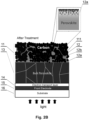
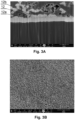
- the SEM image of the cross-section of obtained solar cell structure is shown in Fig. 3A (magnification - 70 000 x), and the top-view SEM image showing perovskite-CuSCN mixed zone (perovskite recrystallized and CuSCN incorporated, through carbon) is show in Fig. 3B (magnification -8000 x).
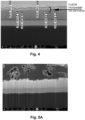
- Fig 4 shows SEM image of perovskite infiltrated (close to its top surface) with CuSCN, with measured thicknesses of the respective layers.
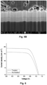
- Fig. 5 represents another embodiment of the present disclosure, wherein Fig. 5A shows SEM image of the cell structure prior to the treatment with the CuSCN material, and Fig. 5B presents the SEM image of the cell structure after infiltration of the CuSCN material through the porous carbon material of the back electrode layer.
- Fig. 5B BHJ zone (perovskite with CuSCN) is clearly visible, whilst in Fig. 5A no BHJ zone is visible.
- Fig. 6 presents current density-voltage characteristics of perovskite solar cells without and after the modification treatment under AM 1.5 illumination and measurement.
- the devices without treatment performed with an efficiency of 10.5%.
- J sc short-circuit current density
- V oc open circuit voltage
Landscapes
- Physics & Mathematics (AREA)
- Electromagnetism (AREA)
- Engineering & Computer Science (AREA)
- Chemical & Material Sciences (AREA)
- Materials Engineering (AREA)
- Manufacturing & Machinery (AREA)
- Inorganic Chemistry (AREA)
- Photovoltaic Devices (AREA)
- Inert Electrodes (AREA)
Claims (15)
- Perowskit-Solarzelle mit einem Schichtenstapel, wobei die Schichten in der folgenden Reihenfolge angeordnet sind: eine Vorderelektrodenschicht (15), eine photoaktive Schicht (13), die ein Perowskitmaterial umfasst, und eine Rückelektrodenschicht (11), die ein poröses Kohlenstoffmaterial mit einer Vielzahl von durchgehenden Poren (111) umfasst, wobei die Solarzelle ferner ein Ladungstransportmaterial (12) umfasst, das dazu konfiguriert ist, die Ladungen zwischen der photoaktiven Schicht (13) und der Rückelektrodenschicht (11) zu transportieren,
dadurch gekennzeichnet, dass
das Ladungstransportmaterial (12) zumindest einige der Vielzahl von durchgehenden Poren (111) des porösen Kohlenstoffmaterials der Rückelektrodenschicht (11) füllt und einen Bulk-Heteroübergang (12a) mit dem Perowskitmaterial der photoaktiven Schicht (13) und eine Grenzfläche (12b) mit dem porösen Kohlenstoffmaterial der Rückelektrodenschicht (11) innerhalb der durchgehenden Poren (111) bildet. - Solarzelle nach Anspruch 1, wobei die Rückelektrodenschicht (11) dazu konfiguriert ist, Löcher zu sammeln, und das Ladungstransportmaterial (12) ein Lochtransportmaterial (HTM) umfasst, das dazu konfiguriert ist, Löcher von der photoaktiven Schicht (13) zu ziehen und zu der Rückelektrodenschicht (11) zu transportieren.
- Solarzelle nach Anspruch 2, wobei das Lochtransportmaterial zumindest eines der Materialien umfasst, die aus der Gruppe ausgewählt sind, die aus Folgendem besteht: CuSCN, Poly(3-hexylthiophen-2,5-diyl) (P3HT), Cu2O und CuI, PTAA und PEDOT:PSS.
- Solarzelle nach Anspruch 2 oder 3, wobei das Lochtransportmaterial ferner mit mindestens einer Passivierungsverbindung vermischt ist.
- Solarzelle nach einem der Ansprüche 2 bis 4, wobei die Vorderelektrodenschicht (15) aus einem Material hergestellt ist, das dazu konfiguriert ist, Elektronen zu sammeln, das aus der Gruppe ausgewählt ist, die aus ITO, IZO, FTO und/oder AZO besteht.
- Solarzelle nach Anspruch 5, wobei der Schichtenstapel ferner eine Elektronentransportschicht (14) zwischen der photoaktiven Schicht (13) und der Vorderelektrodenschicht (15) umfasst.
- Solarzelle nach Anspruch 6, wobei die Elektronentransportschicht (14) ein Material umfasst, das aus der Gruppe ausgewählt ist, die aus SnO2, TiO2, ZnO und PCBM besteht.
- Solarzelle nach einem der vorhergehenden Ansprüche, wobei das poröse Kohlenstoffmaterial der Rückelektrodenschicht (11) einen Wert der spezifischen Oberfläche (SSA) im Bereich von 10 bis 400 m2/g aufweist, gemessen durch ein Brunauer-Emmet-Teller(N2-BET)-Adsorptionsverfahren.
- Solarzelle nach einem der vorhergehenden Ansprüche, wobei die Rückelektrodenschicht (11) vollständig aus dem porösen Kohlenstoffmaterial hergestellt ist.
- Solarzelle nach einem der vorhergehenden Ansprüche, wobei das poröse Kohlenstoffmaterial Graphitflocken einer Partikelgröße von 2 - 9 µm umfasst.
- Solarzelle nach einem der vorhergehenden Ansprüche, wobei die photoaktive Schicht (13) im Wesentlichen vollständig aus einem Perowskitmaterial hergestellt ist, das aus der Gruppe ausgewählt ist, die aus Perowskiten der Formel ABX3 besteht, wobei:A - ein Alkylammonium-Kation oder Metall-Kation wie Cs-Kation ist,B - Pb, Sn oder eine Mischung aus Pb und Sn ist undX - ein Halogenidanion ist, das aus der Gruppe ausgewählt ist, die aus I-, Br- oder Cl- oder einer Mischung davon besteht.
- Verfahren zum Anfertigen einer Perowskit-Solarzelle nach einem der vorhergehenden Ansprüche, umfassend:- Bereitstellen einer Vorderelektrodenschicht (15),- Bilden einer photoaktiven Schicht (13), die ein Perowskitmaterial umfasst, auf der Vorderelektrodenschicht (15),- Bilden einer Rückelektrodenschicht (11), die ein poröses Kohlenstoffmaterial umfasst, das eine Vielzahl von durchgehenden Poren (111) umfasst, direkt auf der photoaktiven Schicht (13),- Füllen der durchgehenden Poren (111) des in dem porösen Kohlenstoffmaterial mit einer Modifizierungslösung, die ein Ladungstransportmaterial (12) und ein Lösungsmittelsystem umfasst, und- Verdampfen des Lösungsmittelsystems aus der Modifizierungslösung.
- Verfahren nach Anspruch 12, wobei das Verdampfen des Lösungsmittelsystems in einem Temperaturbereich von 18 bis 200 C durchgeführt wird und wobei das zu verdampfende Lösungsmittelsystem mindestens eine Komponente umfasst, die aus der Gruppe ausgewählt ist, die aus DMF, DMSO, γ-Butyrolacton (GBL), 2-Methylpyrazin, 2-Methoxyethanol, NMP, DMAC, Acetonitril, Wasser, Ethanol, Isopropanol, Toluol und Chlorbenzol besteht.
- Verfahren nach Anspruch 12 oder 13, wobei das Füllen der offenen Poren unter Verwendung der Modifizierungslösung durchgeführt wird, die das Ladungstransfermaterial umfasst, das aus der Gruppe ausgewählt ist, die aus CuSCN, PTTA, CuSCN, Poly(3-hexylthiophen-2,5-diyl) (P3HT), Cu2O und CuI, PTAA und PEDOT:PSS besteht, wobei die Gesamtkonzentration des Ladungstransfermaterials in der Modifizierungslösung im Bereich von 0,1 bis 100 mg/ml liegt.
- Verfahren nach einem der Ansprüche 12 bis 14, wobei das Füllen der durchgehenden Poren durch ein Verfahren erreicht wird, das aus der Gruppe ausgewählt ist, die aus Gießen, Sprühbeschichten, Tintenstrahldrucken und Schlitzdüsenbeschichten der Modifizierungslösung auf das poröse Kohlenstoffmaterial der Rückelektrodenschicht besteht.
Applications Claiming Priority (2)
| Application Number | Priority Date | Filing Date | Title |
|---|---|---|---|
| EP21461582.5A EP4145547A1 (de) | 2021-09-03 | 2021-09-03 | Perowskit-solarzelle |
| PCT/EP2022/074613 WO2023031456A1 (en) | 2021-09-03 | 2022-09-05 | A perovskite solar cell |
Publications (3)
| Publication Number | Publication Date |
|---|---|
| EP4397155A1 EP4397155A1 (de) | 2024-07-10 |
| EP4397155B1 true EP4397155B1 (de) | 2025-04-02 |
| EP4397155C0 EP4397155C0 (de) | 2025-04-02 |
Family
ID=77640646
Family Applications (2)
| Application Number | Title | Priority Date | Filing Date |
|---|---|---|---|
| EP21461582.5A Withdrawn EP4145547A1 (de) | 2021-09-03 | 2021-09-03 | Perowskit-solarzelle |
| EP22773476.1A Active EP4397155B1 (de) | 2021-09-03 | 2022-09-05 | Perowskit-solarzelle |
Family Applications Before (1)
| Application Number | Title | Priority Date | Filing Date |
|---|---|---|---|
| EP21461582.5A Withdrawn EP4145547A1 (de) | 2021-09-03 | 2021-09-03 | Perowskit-solarzelle |
Country Status (9)
| Country | Link |
|---|---|
| US (1) | US20240373656A1 (de) |
| EP (2) | EP4145547A1 (de) |
| JP (1) | JP2024534227A (de) |
| KR (1) | KR20240088757A (de) |
| CN (1) | CN118077326A (de) |
| CA (1) | CA3230727A1 (de) |
| ES (1) | ES3033111T3 (de) |
| PL (1) | PL4397155T3 (de) |
| WO (1) | WO2023031456A1 (de) |
Families Citing this family (5)
| Publication number | Priority date | Publication date | Assignee | Title |
|---|---|---|---|---|
| EP4380335A1 (de) * | 2022-11-30 | 2024-06-05 | CSEM Centre Suisse d'Electronique et de Microtechnique SA - Recherche et Développement | Verfahren zur herstellung einer perowskit-photovoltaikzelle |
| WO2025089376A1 (ja) * | 2023-10-27 | 2025-05-01 | キヤノン株式会社 | 光電変換素子、光電変換装置、及び光電変換素子の製造方法 |
| WO2025150665A1 (ko) * | 2024-01-08 | 2025-07-17 | 한국화학연구원 | 탄소전극 기반 소자의 제조방법 및 상기 방법으로 제조된 탄소전극 기반 소자 |
| JP2025130236A (ja) * | 2024-02-27 | 2025-09-08 | シャープエネルギーソリューション株式会社 | 太陽電池セル、太陽電池モジュール、およびその製造方法 |
| JP7819227B2 (ja) * | 2024-03-01 | 2026-02-24 | シャープエネルギーソリューション株式会社 | 太陽電池モジュール |
Citations (1)
| Publication number | Priority date | Publication date | Assignee | Title |
|---|---|---|---|---|
| EP3783658A1 (de) * | 2019-08-23 | 2021-02-24 | Saule Spolka Akcyjna | Lichtdurchlässige fotovoltaische vorrichtung und verfahren zur herstellung davon |
Family Cites Families (5)
| Publication number | Priority date | Publication date | Assignee | Title |
|---|---|---|---|---|
| CN104465994A (zh) | 2014-12-09 | 2015-03-25 | 厦门惟华光能有限公司 | 一种基于全涂布工艺的钙钛矿太阳能电池的制备方法 |
| CN106654020B (zh) | 2017-01-24 | 2019-01-08 | 中国科学院上海硅酸盐研究所 | 体异质结钙钛矿薄膜及其制备方法和太阳能电池 |
| CN108574050B (zh) | 2018-07-04 | 2022-02-15 | 河南师范大学 | 一种Perovskite-MoS2体异质结的钙钛矿太阳能电池的制备方法 |
| FI130068B (en) * | 2018-12-31 | 2023-01-31 | Aalto Univ Foundation Sr | Double-sided solar cell unit |
| CN110752299A (zh) | 2019-10-21 | 2020-02-04 | 大连理工大学 | 一种包含钙钛矿-界面连接层的太阳能电池制备方法 |
-
2021
- 2021-09-03 EP EP21461582.5A patent/EP4145547A1/de not_active Withdrawn
-
2022
- 2022-09-05 WO PCT/EP2022/074613 patent/WO2023031456A1/en not_active Ceased
- 2022-09-05 US US18/688,772 patent/US20240373656A1/en active Pending
- 2022-09-05 EP EP22773476.1A patent/EP4397155B1/de active Active
- 2022-09-05 CA CA3230727A patent/CA3230727A1/en active Pending
- 2022-09-05 CN CN202280059921.8A patent/CN118077326A/zh active Pending
- 2022-09-05 ES ES22773476T patent/ES3033111T3/es active Active
- 2022-09-05 KR KR1020247010353A patent/KR20240088757A/ko active Pending
- 2022-09-05 JP JP2024514377A patent/JP2024534227A/ja active Pending
- 2022-09-05 PL PL22773476.1T patent/PL4397155T3/pl unknown
Patent Citations (1)
| Publication number | Priority date | Publication date | Assignee | Title |
|---|---|---|---|---|
| EP3783658A1 (de) * | 2019-08-23 | 2021-02-24 | Saule Spolka Akcyjna | Lichtdurchlässige fotovoltaische vorrichtung und verfahren zur herstellung davon |
Non-Patent Citations (1)
| Title |
|---|
| YOU PENG ET AL: "Efficient Semitransparent Perovskite Solar Cells with Graphene Electrodes - Supporting Information", ADVANCED MATERIALS, vol. 27, no. 24, 12 May 2015 (2015-05-12), DE, pages 3632 - 3638, XP055894668, ISSN: 0935-9648, Retrieved from the Internet <URL:https://onlinelibrary.wiley.com/action/downloadSupplement?doi=10.1002/adma.201501145&file=adma201501145-sup-0001-S1.pdf> DOI: 10.1002/adma.201501145 * |
Also Published As
| Publication number | Publication date |
|---|---|
| JP2024534227A (ja) | 2024-09-18 |
| ES3033111T3 (en) | 2025-07-30 |
| CA3230727A1 (en) | 2023-03-09 |
| WO2023031456A1 (en) | 2023-03-09 |
| CN118077326A (zh) | 2024-05-24 |
| PL4397155T3 (pl) | 2025-07-07 |
| EP4397155A1 (de) | 2024-07-10 |
| EP4145547A1 (de) | 2023-03-08 |
| EP4397155C0 (de) | 2025-04-02 |
| KR20240088757A (ko) | 2024-06-20 |
| US20240373656A1 (en) | 2024-11-07 |
Similar Documents
| Publication | Publication Date | Title |
|---|---|---|
| EP4397155B1 (de) | Perowskit-solarzelle | |
| Lian et al. | Electron‐transport materials in perovskite solar cells | |
| Ciro et al. | Slot-die processing of flexible perovskite solar cells in ambient conditions | |
| Huang et al. | Applications of ZnO in organic and hybrid solar cells | |
| Sun et al. | Room-temperature and solution-processed copper iodide as the hole transport layer for inverted planar perovskite solar cells | |
| Kim et al. | Slot die coated planar perovskite solar cells via blowing and heating assisted one step deposition | |
| KR101949641B1 (ko) | 페로브스카이트막, 이의 제조방법 및 이를 포함하는 태양전지 | |
| CN109904318B (zh) | 一种基于反溶液浴的钙钛矿薄膜制备方法及太阳能电池 | |
| US10546697B2 (en) | Solar cell having light-absorbing structure | |
| KR101571528B1 (ko) | 광전변환효율이 향상된 페로브스카이트 태양전지 및 페로브스카이트 태양전지의 제조방법 | |
| CN107210373A (zh) | 形成钙钛矿光活性器件的光活性层的方法 | |
| CN101176218A (zh) | 聚合物自组织的高效聚合物太阳能电池 | |
| EP4534612A1 (de) | Beschichtungsmittel zur bildung einer grossflächigen perowskit-dünnschicht und verfahren zur bildung einer perowskit-dünnschicht damit | |
| Wang et al. | Interface modification for organic and perovskite solar cells | |
| WO2019243864A1 (en) | Organic solar module and/or fabrication method | |
| CN114975799A (zh) | 一种由p型材料协同掺杂和钝化锡基钙钛矿薄膜的方法及其应用 | |
| KR102298518B1 (ko) | 광전변환율과 안정성이 개선된 탈륨 도핑된 페로브스카이트 태양전지의 제조방법 | |
| CN107978678A (zh) | 一种基于水醇溶性聚合物混合阴极界面层的本体异质结太阳电池及其制备方法 | |
| KR101316237B1 (ko) | 용액 공정 기반의 정공 전도층 제조방법 및 이를 이용한 유기태양전지의 제조방법 | |
| CN103346259A (zh) | 一种有机太阳能电池 | |
| KR102850025B1 (ko) | 탠덤형 실리콘/페로브스카이트 이종접합 태양전지 및 이의 제조방법 | |
| KR101999679B1 (ko) | 페로브스카이트계 태양전지의 제조방법 | |
| KR102934857B1 (ko) | 칼코겐화합물 분자잉크, 이를 이용한 박막태양전지용 광흡수층 및 이를 이용한 박막태양전지 | |
| JP2015029091A (ja) | 有機薄膜太陽電池用光電変換層の製造方法 | |
| KR100981767B1 (ko) | 종형 전계효과 유기 태양전지 |
Legal Events
| Date | Code | Title | Description |
|---|---|---|---|
| STAA | Information on the status of an ep patent application or granted ep patent |
Free format text: STATUS: UNKNOWN |
|
| STAA | Information on the status of an ep patent application or granted ep patent |
Free format text: STATUS: THE INTERNATIONAL PUBLICATION HAS BEEN MADE |
|
| PUAI | Public reference made under article 153(3) epc to a published international application that has entered the european phase |
Free format text: ORIGINAL CODE: 0009012 |
|
| STAA | Information on the status of an ep patent application or granted ep patent |
Free format text: STATUS: REQUEST FOR EXAMINATION WAS MADE |
|
| 17P | Request for examination filed |
Effective date: 20240325 |
|
| AK | Designated contracting states |
Kind code of ref document: A1 Designated state(s): AL AT BE BG CH CY CZ DE DK EE ES FI FR GB GR HR HU IE IS IT LI LT LU LV MC MK MT NL NO PL PT RO RS SE SI SK SM TR |
|
| GRAP | Despatch of communication of intention to grant a patent |
Free format text: ORIGINAL CODE: EPIDOSNIGR1 |
|
| STAA | Information on the status of an ep patent application or granted ep patent |
Free format text: STATUS: GRANT OF PATENT IS INTENDED |
|
| DAV | Request for validation of the european patent (deleted) | ||
| DAX | Request for extension of the european patent (deleted) | ||
| INTG | Intention to grant announced |
Effective date: 20241023 |
|
| GRAS | Grant fee paid |
Free format text: ORIGINAL CODE: EPIDOSNIGR3 |
|
| GRAA | (expected) grant |
Free format text: ORIGINAL CODE: 0009210 |
|
| STAA | Information on the status of an ep patent application or granted ep patent |
Free format text: STATUS: THE PATENT HAS BEEN GRANTED |
|
| AK | Designated contracting states |
Kind code of ref document: B1 Designated state(s): AL AT BE BG CH CY CZ DE DK EE ES FI FR GB GR HR HU IE IS IT LI LT LU LV MC MK MT NL NO PL PT RO RS SE SI SK SM TR |
|
| REG | Reference to a national code |
Ref country code: GB Ref legal event code: FG4D |
|
| REG | Reference to a national code |
Ref country code: CH Ref legal event code: EP |
|
| REG | Reference to a national code |
Ref country code: IE Ref legal event code: FG4D |
|
| REG | Reference to a national code |
Ref country code: DE Ref legal event code: R096 Ref document number: 602022012683 Country of ref document: DE |
|
| U01 | Request for unitary effect filed |
Effective date: 20250423 |
|
| U07 | Unitary effect registered |
Designated state(s): AT BE BG DE DK EE FI FR IT LT LU LV MT NL PT RO SE SI Effective date: 20250430 |
|
| REG | Reference to a national code |
Ref country code: ES Ref legal event code: FG2A Ref document number: 3033111 Country of ref document: ES Kind code of ref document: T3 Effective date: 20250730 |
|
| REG | Reference to a national code |
Ref country code: CH Ref legal event code: U11 Free format text: ST27 STATUS EVENT CODE: U-0-0-U10-U11 (AS PROVIDED BY THE NATIONAL OFFICE) Effective date: 20251001 |
|
| PG25 | Lapsed in a contracting state [announced via postgrant information from national office to epo] |
Ref country code: NO Free format text: LAPSE BECAUSE OF FAILURE TO SUBMIT A TRANSLATION OF THE DESCRIPTION OR TO PAY THE FEE WITHIN THE PRESCRIBED TIME-LIMIT Effective date: 20250702 Ref country code: GR Free format text: LAPSE BECAUSE OF FAILURE TO SUBMIT A TRANSLATION OF THE DESCRIPTION OR TO PAY THE FEE WITHIN THE PRESCRIBED TIME-LIMIT Effective date: 20250703 |
|
| PGFP | Annual fee paid to national office [announced via postgrant information from national office to epo] |
Ref country code: PL Payment date: 20250819 Year of fee payment: 4 |
|
| PG25 | Lapsed in a contracting state [announced via postgrant information from national office to epo] |
Ref country code: HR Free format text: LAPSE BECAUSE OF FAILURE TO SUBMIT A TRANSLATION OF THE DESCRIPTION OR TO PAY THE FEE WITHIN THE PRESCRIBED TIME-LIMIT Effective date: 20250402 |
|
| PG25 | Lapsed in a contracting state [announced via postgrant information from national office to epo] |
Ref country code: RS Free format text: LAPSE BECAUSE OF FAILURE TO SUBMIT A TRANSLATION OF THE DESCRIPTION OR TO PAY THE FEE WITHIN THE PRESCRIBED TIME-LIMIT Effective date: 20250702 |
|
| PG25 | Lapsed in a contracting state [announced via postgrant information from national office to epo] |
Ref country code: IS Free format text: LAPSE BECAUSE OF FAILURE TO SUBMIT A TRANSLATION OF THE DESCRIPTION OR TO PAY THE FEE WITHIN THE PRESCRIBED TIME-LIMIT Effective date: 20250802 |
|
| U20 | Renewal fee for the european patent with unitary effect paid |
Year of fee payment: 4 Effective date: 20250929 |
|
| PG25 | Lapsed in a contracting state [announced via postgrant information from national office to epo] |
Ref country code: SM Free format text: LAPSE BECAUSE OF FAILURE TO SUBMIT A TRANSLATION OF THE DESCRIPTION OR TO PAY THE FEE WITHIN THE PRESCRIBED TIME-LIMIT Effective date: 20250402 |
|
| PGFP | Annual fee paid to national office [announced via postgrant information from national office to epo] |
Ref country code: CH Payment date: 20251001 Year of fee payment: 4 |
|
| PG25 | Lapsed in a contracting state [announced via postgrant information from national office to epo] |
Ref country code: CZ Free format text: LAPSE BECAUSE OF FAILURE TO SUBMIT A TRANSLATION OF THE DESCRIPTION OR TO PAY THE FEE WITHIN THE PRESCRIBED TIME-LIMIT Effective date: 20250402 |
|
| PG25 | Lapsed in a contracting state [announced via postgrant information from national office to epo] |
Ref country code: SK Free format text: LAPSE BECAUSE OF FAILURE TO SUBMIT A TRANSLATION OF THE DESCRIPTION OR TO PAY THE FEE WITHIN THE PRESCRIBED TIME-LIMIT Effective date: 20250402 |
|
| PGFP | Annual fee paid to national office [announced via postgrant information from national office to epo] |
Ref country code: ES Payment date: 20251001 Year of fee payment: 4 |
|
| PLBE | No opposition filed within time limit |
Free format text: ORIGINAL CODE: 0009261 |
|
| STAA | Information on the status of an ep patent application or granted ep patent |
Free format text: STATUS: NO OPPOSITION FILED WITHIN TIME LIMIT |
|
| REG | Reference to a national code |
Ref country code: CH Ref legal event code: L10 Free format text: ST27 STATUS EVENT CODE: U-0-0-L10-L00 (AS PROVIDED BY THE NATIONAL OFFICE) Effective date: 20260211 |
|
| 26N | No opposition filed |
Effective date: 20260105 |