EP4394871A2 - Anzeigetafel und anzeigevorrichtung damit - Google Patents
Anzeigetafel und anzeigevorrichtung damit Download PDFInfo
- Publication number
- EP4394871A2 EP4394871A2 EP23216674.4A EP23216674A EP4394871A2 EP 4394871 A2 EP4394871 A2 EP 4394871A2 EP 23216674 A EP23216674 A EP 23216674A EP 4394871 A2 EP4394871 A2 EP 4394871A2
- Authority
- EP
- European Patent Office
- Prior art keywords
- disposed
- layer
- pixel
- electrode
- pixels
- Prior art date
- Legal status (The legal status is an assumption and is not a legal conclusion. Google has not performed a legal analysis and makes no representation as to the accuracy of the status listed.)
- Pending
Links
Images



Classifications
-
- G—PHYSICS
- G09—EDUCATION; CRYPTOGRAPHY; DISPLAY; ADVERTISING; SEALS
- G09G—ARRANGEMENTS OR CIRCUITS FOR CONTROL OF INDICATING DEVICES USING STATIC MEANS TO PRESENT VARIABLE INFORMATION
- G09G3/00—Control arrangements or circuits, of interest only in connection with visual indicators other than cathode-ray tubes
- G09G3/20—Control arrangements or circuits, of interest only in connection with visual indicators other than cathode-ray tubes for presentation of an assembly of a number of characters, e.g. a page, by composing the assembly by combination of individual elements arranged in a matrix no fixed position being assigned to or needed to be assigned to the individual characters or partial characters
- G09G3/22—Control arrangements or circuits, of interest only in connection with visual indicators other than cathode-ray tubes for presentation of an assembly of a number of characters, e.g. a page, by composing the assembly by combination of individual elements arranged in a matrix no fixed position being assigned to or needed to be assigned to the individual characters or partial characters using controlled light sources
- G09G3/30—Control arrangements or circuits, of interest only in connection with visual indicators other than cathode-ray tubes for presentation of an assembly of a number of characters, e.g. a page, by composing the assembly by combination of individual elements arranged in a matrix no fixed position being assigned to or needed to be assigned to the individual characters or partial characters using controlled light sources using electroluminescent panels
- G09G3/32—Control arrangements or circuits, of interest only in connection with visual indicators other than cathode-ray tubes for presentation of an assembly of a number of characters, e.g. a page, by composing the assembly by combination of individual elements arranged in a matrix no fixed position being assigned to or needed to be assigned to the individual characters or partial characters using controlled light sources using electroluminescent panels semiconductive, e.g. using light-emitting diodes [LED]
- G09G3/3208—Control arrangements or circuits, of interest only in connection with visual indicators other than cathode-ray tubes for presentation of an assembly of a number of characters, e.g. a page, by composing the assembly by combination of individual elements arranged in a matrix no fixed position being assigned to or needed to be assigned to the individual characters or partial characters using controlled light sources using electroluminescent panels semiconductive, e.g. using light-emitting diodes [LED] organic, e.g. using organic light-emitting diodes [OLED]
-
- H—ELECTRICITY
- H10—SEMICONDUCTOR DEVICES; ELECTRIC SOLID-STATE DEVICES NOT OTHERWISE PROVIDED FOR
- H10W—GENERIC PACKAGES, INTERCONNECTIONS, CONNECTORS OR OTHER CONSTRUCTIONAL DETAILS OF DEVICES COVERED BY CLASS H10
- H10W90/00—Package configurations
-
- H—ELECTRICITY
- H10—SEMICONDUCTOR DEVICES; ELECTRIC SOLID-STATE DEVICES NOT OTHERWISE PROVIDED FOR
- H10D—INORGANIC ELECTRIC SEMICONDUCTOR DEVICES
- H10D86/00—Integrated devices formed in or on insulating or conducting substrates, e.g. formed in silicon-on-insulator [SOI] substrates or on stainless steel or glass substrates
- H10D86/40—Integrated devices formed in or on insulating or conducting substrates, e.g. formed in silicon-on-insulator [SOI] substrates or on stainless steel or glass substrates characterised by multiple TFTs
- H10D86/441—Interconnections, e.g. scanning lines
-
- G—PHYSICS
- G09—EDUCATION; CRYPTOGRAPHY; DISPLAY; ADVERTISING; SEALS
- G09G—ARRANGEMENTS OR CIRCUITS FOR CONTROL OF INDICATING DEVICES USING STATIC MEANS TO PRESENT VARIABLE INFORMATION
- G09G3/00—Control arrangements or circuits, of interest only in connection with visual indicators other than cathode-ray tubes
- G09G3/20—Control arrangements or circuits, of interest only in connection with visual indicators other than cathode-ray tubes for presentation of an assembly of a number of characters, e.g. a page, by composing the assembly by combination of individual elements arranged in a matrix no fixed position being assigned to or needed to be assigned to the individual characters or partial characters
- G09G3/22—Control arrangements or circuits, of interest only in connection with visual indicators other than cathode-ray tubes for presentation of an assembly of a number of characters, e.g. a page, by composing the assembly by combination of individual elements arranged in a matrix no fixed position being assigned to or needed to be assigned to the individual characters or partial characters using controlled light sources
- G09G3/30—Control arrangements or circuits, of interest only in connection with visual indicators other than cathode-ray tubes for presentation of an assembly of a number of characters, e.g. a page, by composing the assembly by combination of individual elements arranged in a matrix no fixed position being assigned to or needed to be assigned to the individual characters or partial characters using controlled light sources using electroluminescent panels
- G09G3/32—Control arrangements or circuits, of interest only in connection with visual indicators other than cathode-ray tubes for presentation of an assembly of a number of characters, e.g. a page, by composing the assembly by combination of individual elements arranged in a matrix no fixed position being assigned to or needed to be assigned to the individual characters or partial characters using controlled light sources using electroluminescent panels semiconductive, e.g. using light-emitting diodes [LED]
-
- G—PHYSICS
- G09—EDUCATION; CRYPTOGRAPHY; DISPLAY; ADVERTISING; SEALS
- G09G—ARRANGEMENTS OR CIRCUITS FOR CONTROL OF INDICATING DEVICES USING STATIC MEANS TO PRESENT VARIABLE INFORMATION
- G09G3/00—Control arrangements or circuits, of interest only in connection with visual indicators other than cathode-ray tubes
- G09G3/20—Control arrangements or circuits, of interest only in connection with visual indicators other than cathode-ray tubes for presentation of an assembly of a number of characters, e.g. a page, by composing the assembly by combination of individual elements arranged in a matrix no fixed position being assigned to or needed to be assigned to the individual characters or partial characters
- G09G3/22—Control arrangements or circuits, of interest only in connection with visual indicators other than cathode-ray tubes for presentation of an assembly of a number of characters, e.g. a page, by composing the assembly by combination of individual elements arranged in a matrix no fixed position being assigned to or needed to be assigned to the individual characters or partial characters using controlled light sources
- G09G3/30—Control arrangements or circuits, of interest only in connection with visual indicators other than cathode-ray tubes for presentation of an assembly of a number of characters, e.g. a page, by composing the assembly by combination of individual elements arranged in a matrix no fixed position being assigned to or needed to be assigned to the individual characters or partial characters using controlled light sources using electroluminescent panels
- G09G3/32—Control arrangements or circuits, of interest only in connection with visual indicators other than cathode-ray tubes for presentation of an assembly of a number of characters, e.g. a page, by composing the assembly by combination of individual elements arranged in a matrix no fixed position being assigned to or needed to be assigned to the individual characters or partial characters using controlled light sources using electroluminescent panels semiconductive, e.g. using light-emitting diodes [LED]
- G09G3/3208—Control arrangements or circuits, of interest only in connection with visual indicators other than cathode-ray tubes for presentation of an assembly of a number of characters, e.g. a page, by composing the assembly by combination of individual elements arranged in a matrix no fixed position being assigned to or needed to be assigned to the individual characters or partial characters using controlled light sources using electroluminescent panels semiconductive, e.g. using light-emitting diodes [LED] organic, e.g. using organic light-emitting diodes [OLED]
- G09G3/3225—Control arrangements or circuits, of interest only in connection with visual indicators other than cathode-ray tubes for presentation of an assembly of a number of characters, e.g. a page, by composing the assembly by combination of individual elements arranged in a matrix no fixed position being assigned to or needed to be assigned to the individual characters or partial characters using controlled light sources using electroluminescent panels semiconductive, e.g. using light-emitting diodes [LED] organic, e.g. using organic light-emitting diodes [OLED] using an active matrix
- G09G3/3258—Control arrangements or circuits, of interest only in connection with visual indicators other than cathode-ray tubes for presentation of an assembly of a number of characters, e.g. a page, by composing the assembly by combination of individual elements arranged in a matrix no fixed position being assigned to or needed to be assigned to the individual characters or partial characters using controlled light sources using electroluminescent panels semiconductive, e.g. using light-emitting diodes [LED] organic, e.g. using organic light-emitting diodes [OLED] using an active matrix with pixel circuitry controlling the voltage across the light-emitting element
-
- H—ELECTRICITY
- H10—SEMICONDUCTOR DEVICES; ELECTRIC SOLID-STATE DEVICES NOT OTHERWISE PROVIDED FOR
- H10D—INORGANIC ELECTRIC SEMICONDUCTOR DEVICES
- H10D86/00—Integrated devices formed in or on insulating or conducting substrates, e.g. formed in silicon-on-insulator [SOI] substrates or on stainless steel or glass substrates
- H10D86/40—Integrated devices formed in or on insulating or conducting substrates, e.g. formed in silicon-on-insulator [SOI] substrates or on stainless steel or glass substrates characterised by multiple TFTs
- H10D86/60—Integrated devices formed in or on insulating or conducting substrates, e.g. formed in silicon-on-insulator [SOI] substrates or on stainless steel or glass substrates characterised by multiple TFTs wherein the TFTs are in active matrices
-
- H—ELECTRICITY
- H10—SEMICONDUCTOR DEVICES; ELECTRIC SOLID-STATE DEVICES NOT OTHERWISE PROVIDED FOR
- H10D—INORGANIC ELECTRIC SEMICONDUCTOR DEVICES
- H10D89/00—Aspects of integrated devices not covered by groups H10D84/00 - H10D88/00
- H10D89/60—Integrated devices comprising arrangements for electrical or thermal protection, e.g. protection circuits against electrostatic discharge [ESD]
-
- H—ELECTRICITY
- H10—SEMICONDUCTOR DEVICES; ELECTRIC SOLID-STATE DEVICES NOT OTHERWISE PROVIDED FOR
- H10H—INORGANIC LIGHT-EMITTING SEMICONDUCTOR DEVICES HAVING POTENTIAL BARRIERS
- H10H20/00—Individual inorganic light-emitting semiconductor devices having potential barriers, e.g. light-emitting diodes [LED]
- H10H20/80—Constructional details
- H10H20/83—Electrodes
- H10H20/831—Electrodes characterised by their shape
-
- H—ELECTRICITY
- H10—SEMICONDUCTOR DEVICES; ELECTRIC SOLID-STATE DEVICES NOT OTHERWISE PROVIDED FOR
- H10H—INORGANIC LIGHT-EMITTING SEMICONDUCTOR DEVICES HAVING POTENTIAL BARRIERS
- H10H20/00—Individual inorganic light-emitting semiconductor devices having potential barriers, e.g. light-emitting diodes [LED]
- H10H20/80—Constructional details
- H10H20/85—Packages
- H10H20/855—Optical field-shaping means, e.g. lenses
-
- H—ELECTRICITY
- H10—SEMICONDUCTOR DEVICES; ELECTRIC SOLID-STATE DEVICES NOT OTHERWISE PROVIDED FOR
- H10H—INORGANIC LIGHT-EMITTING SEMICONDUCTOR DEVICES HAVING POTENTIAL BARRIERS
- H10H20/00—Individual inorganic light-emitting semiconductor devices having potential barriers, e.g. light-emitting diodes [LED]
- H10H20/80—Constructional details
- H10H20/85—Packages
- H10H20/857—Interconnections, e.g. lead-frames, bond wires or solder balls
-
- H—ELECTRICITY
- H10—SEMICONDUCTOR DEVICES; ELECTRIC SOLID-STATE DEVICES NOT OTHERWISE PROVIDED FOR
- H10H—INORGANIC LIGHT-EMITTING SEMICONDUCTOR DEVICES HAVING POTENTIAL BARRIERS
- H10H29/00—Integrated devices, or assemblies of multiple devices, comprising at least one light-emitting semiconductor element covered by group H10H20/00
- H10H29/10—Integrated devices comprising at least one light-emitting semiconductor component covered by group H10H20/00
- H10H29/14—Integrated devices comprising at least one light-emitting semiconductor component covered by group H10H20/00 comprising multiple light-emitting semiconductor components
- H10H29/142—Two-dimensional arrangements, e.g. asymmetric LED layout
-
- H—ELECTRICITY
- H10—SEMICONDUCTOR DEVICES; ELECTRIC SOLID-STATE DEVICES NOT OTHERWISE PROVIDED FOR
- H10K—ORGANIC ELECTRIC SOLID-STATE DEVICES
- H10K59/00—Integrated devices, or assemblies of multiple devices, comprising at least one organic light-emitting element covered by group H10K50/00
- H10K59/10—OLED displays
- H10K59/12—Active-matrix OLED [AMOLED] displays
- H10K59/122—Pixel-defining structures or layers, e.g. banks
-
- H—ELECTRICITY
- H10—SEMICONDUCTOR DEVICES; ELECTRIC SOLID-STATE DEVICES NOT OTHERWISE PROVIDED FOR
- H10K—ORGANIC ELECTRIC SOLID-STATE DEVICES
- H10K59/00—Integrated devices, or assemblies of multiple devices, comprising at least one organic light-emitting element covered by group H10K50/00
- H10K59/10—OLED displays
- H10K59/12—Active-matrix OLED [AMOLED] displays
- H10K59/131—Interconnections, e.g. wiring lines or terminals
-
- H—ELECTRICITY
- H10—SEMICONDUCTOR DEVICES; ELECTRIC SOLID-STATE DEVICES NOT OTHERWISE PROVIDED FOR
- H10K—ORGANIC ELECTRIC SOLID-STATE DEVICES
- H10K59/00—Integrated devices, or assemblies of multiple devices, comprising at least one organic light-emitting element covered by group H10K50/00
- H10K59/30—Devices specially adapted for multicolour light emission
- H10K59/35—Devices specially adapted for multicolour light emission comprising red-green-blue [RGB] subpixels
-
- H—ELECTRICITY
- H10—SEMICONDUCTOR DEVICES; ELECTRIC SOLID-STATE DEVICES NOT OTHERWISE PROVIDED FOR
- H10K—ORGANIC ELECTRIC SOLID-STATE DEVICES
- H10K59/00—Integrated devices, or assemblies of multiple devices, comprising at least one organic light-emitting element covered by group H10K50/00
- H10K59/30—Devices specially adapted for multicolour light emission
- H10K59/35—Devices specially adapted for multicolour light emission comprising red-green-blue [RGB] subpixels
- H10K59/351—Devices specially adapted for multicolour light emission comprising red-green-blue [RGB] subpixels comprising more than three subpixels, e.g. red-green-blue-white [RGBW]
-
- H—ELECTRICITY
- H10—SEMICONDUCTOR DEVICES; ELECTRIC SOLID-STATE DEVICES NOT OTHERWISE PROVIDED FOR
- H10K—ORGANIC ELECTRIC SOLID-STATE DEVICES
- H10K59/00—Integrated devices, or assemblies of multiple devices, comprising at least one organic light-emitting element covered by group H10K50/00
- H10K59/80—Constructional details
- H10K59/805—Electrodes
-
- H—ELECTRICITY
- H10—SEMICONDUCTOR DEVICES; ELECTRIC SOLID-STATE DEVICES NOT OTHERWISE PROVIDED FOR
- H10K—ORGANIC ELECTRIC SOLID-STATE DEVICES
- H10K59/00—Integrated devices, or assemblies of multiple devices, comprising at least one organic light-emitting element covered by group H10K50/00
- H10K59/80—Constructional details
- H10K59/875—Arrangements for extracting light from the devices
-
- H—ELECTRICITY
- H10—SEMICONDUCTOR DEVICES; ELECTRIC SOLID-STATE DEVICES NOT OTHERWISE PROVIDED FOR
- H10W—GENERIC PACKAGES, INTERCONNECTIONS, CONNECTORS OR OTHER CONSTRUCTIONAL DETAILS OF DEVICES COVERED BY CLASS H10
- H10W42/00—Arrangements for protection of devices
- H10W42/60—Arrangements for protection of devices protecting against electrostatic charges or discharges, e.g. Faraday shields
-
- G—PHYSICS
- G09—EDUCATION; CRYPTOGRAPHY; DISPLAY; ADVERTISING; SEALS
- G09G—ARRANGEMENTS OR CIRCUITS FOR CONTROL OF INDICATING DEVICES USING STATIC MEANS TO PRESENT VARIABLE INFORMATION
- G09G2300/00—Aspects of the constitution of display devices
- G09G2300/04—Structural and physical details of display devices
- G09G2300/0421—Structural details of the set of electrodes
- G09G2300/0426—Layout of electrodes and connections
-
- G—PHYSICS
- G09—EDUCATION; CRYPTOGRAPHY; DISPLAY; ADVERTISING; SEALS
- G09G—ARRANGEMENTS OR CIRCUITS FOR CONTROL OF INDICATING DEVICES USING STATIC MEANS TO PRESENT VARIABLE INFORMATION
- G09G2300/00—Aspects of the constitution of display devices
- G09G2300/04—Structural and physical details of display devices
- G09G2300/0439—Pixel structures
-
- G—PHYSICS
- G09—EDUCATION; CRYPTOGRAPHY; DISPLAY; ADVERTISING; SEALS
- G09G—ARRANGEMENTS OR CIRCUITS FOR CONTROL OF INDICATING DEVICES USING STATIC MEANS TO PRESENT VARIABLE INFORMATION
- G09G2330/00—Aspects of power supply; Aspects of display protection and defect management
- G09G2330/06—Handling electromagnetic interferences [EMI], covering emitted as well as received electromagnetic radiation
Definitions
- the present disclosure relates to a display panel and a display device including the same.
- a display device with a self-light-emitting element may be implemented to be thinner than a display device with a built-in light source, and has the advantage of being able to implement a flexible and foldable display device.
- Such a display device having the self-light-emitting element may include an organic light-emitting display device using a light-emissive layer made of an organic material, and a micro-LED display device using a micro light-emitting diode.
- the micro light-emitting diode is a semiconductor light-emitting element that uses property of emitting light when current flows through a semiconductor, and is widely used in a lighting apparatus, TV, and various display devices.
- the display device using the micro light-emitting diode does not have semiconductor (a-Si), oxide, and low-temperature polycrystalline silicon (LTPS) layers.
- a-Si semiconductor
- LTPS low-temperature polycrystalline silicon
- ESD electrostatic discharge
- the inventor of the present disclosure has invented a display panel in which a light-emitting element disposed in a bezel area but not used as a pixel acts as an element that copes with the static electricity.
- a technical purpose to be achieved by the present disclosure is to provide a display panel in which a static electricity coping electrode is disposed at each of the light-emitting elements disposed in the bezel area of the display panel such that each of the light-emitting elements at which the static electricity coping electrode is disposed acts as a static electricity coping area, and to provide a display device that includes the display panel.
- a display device includes a display panel including: at least one first pixel disposed in a first area; and at least one second pixel disposed in a second area; and a driver disposed on a rear surface of the display panel and in the first area, wherein the driver controls a light-emission operation of the at least one first pixel, wherein the at least one first pixel includes at least one sub-pixel, wherein each of the at least one sub-pixel thereof has a first electrode at one side and a second electrode at an opposite side thereto, wherein the at least one second pixel includes at least one sub-pixel, wherein each of the at least one sub-pixel thereof has a first electrode at one side and a second electrode at an opposite side thereto, wherein the second electrode acts as a power supply electrode, wherein the first electrode of the sub-pixel of the at least one second pixel is connected to a ground, and the second electrode thereof as the power supply electrode is connected to a power supply line, wherein the at
- unused light-emitting elements disposed in the bezel area may be utilized as the electrostatic discharge (ESD) circuit.
- a separate electrostatic discharge (ESD) circuit is not installed, but unused light-emitting elements disposed in the bezel area may be utilized as the electrostatic discharge (ESD) circuit.
- ESD electrostatic discharge
- panel damage caused by the static electricity may be prevented, thereby improving the quality and reliability of the display device.
- unused light-emitting elements disposed in the bezel area may be utilized as the electrostatic discharge (ESD) circuit to secure reliability of the display device and to implement a stable narrow bezel.
- ESD electrostatic discharge
- a display panel comprises a plurality of bezel area pixels disposed in a bezel area of the display panel surrounding at least a part of an active area, one or more of the bezel area pixels each including one or more bezel area sub-pixels configured not to emit light, wherein the bezel area sub-pixels comprise: a first bezel area sub-pixel having a first electrode and a second electrode, the first electrode electrically connected to a common node and the second electrode electrically connected to a first power supply line; and a second bezel area sub-pixel having a third electrode and a fourth electrode, the third electrode electrically connected to the common node and the fourth electrode electrically connected to a second power supply line different from the first power supply line.
- first element or layer when a first element or layer is referred to as being present "on" a second element or layer, the first element may be disposed directly on the second element or may be disposed indirectly on the second element with a third element or layer being disposed between the first and second elements or layers.
- a layer, film, region, plate, or the like when a layer, film, region, plate, or the like may be disposed “below” or “under” another layer, film, region, plate, or the like, the former may directly contact the latter or still another layer, film, region, plate, or the like may be disposed between the former and the latter.
- the former when a layer, film, region, plate, or the like is directly disposed “below” or “under” another layer, film, region, plate, or the like, the former directly contacts the latter and still another layer, film, region, plate, or the like is not disposed between the former and the latter.
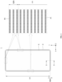
- the display device 1 may include the display panel 5.
- the display panel 5 may include the display module disposed on the rear surface of the cover member 3. Since the cover member 3 includes a display area AA that displays a screen, the cover member 3 may be made of a transparent material such as a cover glass to display the screen therethrough.
- the cover member 3 may be made of a transparent plastic material, a glass material, or a tempered glass material.
- the back frame may function as a casing constituting the outermost portion of the display device 1.
- the present disclosure is not limited thereto.
- the back frame may function as a middle frame serving as a housing protecting the rear surface of the display module.
- Each of the first pixel P1 and the second pixel P2 may include one or more sub-pixels.
- Each of the first pixel P1 and the second pixel P2 may include or may be a sub-pixel SP emitting red, blue, or green light.
- the present disclosure is not limited thereto.
- each of the first pixel P1 and the second pixel P2 may include or may be a sub-pixel emitting white light.
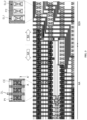
- FIG. 2A is a cross-sectional view of the first pixel disposed in the display area according to an embodiment of the present disclosure, and more specifically a cross-sectional view taken along line A-A' of FIG. 3 .
- FIG. 2B is a cross-sectional view of the second pixel disposed in the bezel area according to an embodiment of the present disclosure and more specifically a cross-sectional view taken along line B-B' of FIG. 5A .
- the power supply electrode 22 may be disposed on the sidewall diffuser layer 24 and the active layer 20.
- the power supply electrode 22 may be the high-potential voltage (VDD) electrode or the low-potential voltage (VSS) electrode.
- the shock power may flow from the first signal line SL1 or the second signal line SL2 to the first power wiring plate VDD or the second power wiring plate VSS due to the second pixel P2 disposed in the second area BZA. Accordingly, damage to the display panel 5 due to the static electricity may be prevented.
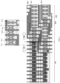
- FIG. 5A is a diagram showing a connection structure of at least one second pixel disposed in the second area of the display panel according to an embodiment of the present disclosure.
- FIG. 5B is a diagram showing an example of an ESD circuit implemented based on the connection structure of the at least one second pixel in FIG. 5A .
- the ESD circuit based on the connection structure of the second pixel P2 has the signal line SL1 or SL2 disposed at one side thereof.
- two second pixels P2 may operate as a first diode D1 and a second diode D2, respectively.
- the high power voltage (VDD) line is connected to the first diode D1
- the low-potential voltage (VSS) line is connected to the second diode D2.
- the first signal line SL1 and the second signal line SL2 may be connected to some of the second pixels P2 and may surround the upper surface and both opposing walls of the bank layer 26. This may be the same as the description of FIG. 2B as set forth above, which illustrates the cross section of B-B'.
- each element of the first pixel P1 has the first electrode disposed on the bank layer so as to cover the upper surface of the bank layer and one side wall of the bank layer.
- the signal line (SL1 or SL2) is connected to one side of the ESD circuit.
- the first diode D1 is connected to this signal line (SL1 or SL2) via a resistor R1, and is connected to the low-potential voltage (VSS) line at an upper position.
- the second diode D2 is connected to the signal line (SL1 or SL2) via the resistor R1, and is connected to the high-potential voltage (VDD) line at a lower position.
- the light-emitting element LE of the second pixel P2 does not function as a light-emitting element LE that outputs light, but may perform a function of the first diode D1 or the second diode D2 having the characteristics as shown in FIG. 7.
- the first electrode and the second electrode may be referred to as a n-type electrode and a p-type electrode.
- the first electrode and the second electrode are a p-type electrode and an n-type electrode, respectively will be described.
- Each of the first and second electrodes according to an embodiment of the present disclosure may include one or more of metal materials such as Au, W, Pt, Si, Ir, Ag, Cu, Ni, Ti, or Cr and alloys thereof.
- Each of the first electrode and the second electrode according to another embodiment may be made of a transparent conductive material, and the transparent conductive material may include ITO (Indium Tin Oxide) or IZO (Indium Zinc Oxide).
- ITO Indium Tin Oxide
- IZO Indium Zinc Oxide
- the insulating film may be disposed to cover an outer surface of the light-emitting element and may have an insulating film open area (P-Open) defined therein to expose at least a portion of each of the first electrode and the second electrode.
- the insulating film may be made of a material such as SiNx or SiOx and may be disposed to cover the active layer.
- the p-type electrode and the n-type electrode in the light-emitting element may be injected from the n-type GaN layer and the p-type GaN layer to the active layer, respectively.
- excitons may be generated in the active layer.
- light corresponding to an energy difference between the LUMO (Lowest Unoccupied Molecular Orbital) level and the HOMO (Highest Occupied Molecular Orbital) level of the light-emissive layer may be generated and emitted to the outside.
- the light-emitting element may be formed to have a size of about 10 to 100 ⁇ m.
- the light-emitting element may be fabricated by forming a buffer layer on a substrate 110 and growing a GaN thin-film on the buffer layer.
- sapphire, silicon (Si), GaN, silicon carbide (SiC), gallium arsenide (GaAs), zinc oxide (ZnO), etc. may be used as a material of the substrate for the growth of the GaN thin-film.
- the buffer layer may be provided to prevent or reduce quality deterioration due to the lattice mismatch and may be made of AlN or GaN.
- the n-type GaN layer may be formed by growing a GaN layer not doped with impurities and then doping an n-type impurity such as silicon (Si) into a top portion of the undoped GaN layer. Further, a p-type GaN layer may be formed by growing an undoped GaN thin-film and then doping p-type impurities such as Mg, Zn, and Be into the undoped GaN thin-film.
- each of the first sub-pixel R to the fourth sub-pixel W may be disposed in a flip scheme.
- the flip scheme may refer to a scheme in which when the light-emitting element is, for example, a micro-LED chip, first and second electrodes of the chip are turned upside down.
- Each fifth sub-pixel may emit light of the same color as a color of light emitted from the sub-pixel corresponding to each spare area.
- a display panel in which a light-emitting element disposed in a bezel area BZA but not used as a pixel may be used as an element that copes with static electricity may be realized.
- the common node is electrically connected to a common voltage connected to electrodes of the active area sub-pixels.
- the common node is electrically connected to a data line driving data voltages to electrodes of the active area sub-pixels.
- At least one of the active area sub-pixels comprises: an anode disposed on a bank layer so as to cover an upper surface and one side wall of the bank layer, a diffuser window layer disposed on the anode and the bank layer, a conductive layer disposed on the anode, an active layer disposed on the conductive layer, a sidewall diffuser layer disposed on the diffuser window layer so as to surround the conductive layer and the active layer, and a cathode disposed on the sidewall diffuser layer and the active layer.
- At least one of the bezel area sub-pixels comprises: an anode disposed on a bank layer so as to cover an upper surface and both side wall surfaces of the bank layer, a diffuser window layer disposed on the anode, a conductive layer disposed on the anode, an active layer disposed on the conductive layer, a sidewall diffuser layer disposed on the diffuser window layer so as to surround the conductive layer and the active layer, and a cathode disposed on the sidewall diffuser layer and the active layer.
- a display device comprising: the display panel described herein above; and a driver disposed on a rear surface of the display panel in the active area, wherein the driver is configured to control an amount of light emitted from the active area sub-pixels.
- the driver is configured to apply a data voltage set during a first control period to each of the one or more active area sub-pixels of the active area pixels to cause each active area sub-pixel to emit light corresponding to a generated coordinate value for a pulse width set during a second control period.
- a spare area is disposed around each of the active area pixels and the bezel area pixels.
- a display device comprising: a display panel including: at least one first pixel disposed in a first area; and at least one second pixel disposed in a second area; and a driver disposed on a rear surface of the display panel in the first area, wherein the driver controls a light-emission operation of the at least one first pixel, wherein the first pixel includes at least one sub-pixel, wherein each of the at least one sub-pixel thereof has a first electrode at one side and a second electrode at the other side thereto, wherein the second pixel includes at least one sub-pixel, wherein each of the at least one sub-pixel thereof has a first electrode at one side and a power supply electrode at the other side thereto, wherein the first electrode of the sub-pixel of the second pixel is connected to a ground, and the power supply electrode is connected to a power supply line, wherein the first pixel and the second pixel operate at voltages of different potentials, respectively.
- the at least one sub-pixel of the first pixel is configured to emit light of one color of red, green, blue, and white.
- the first area is a display area and the second area is a bezel area.
Landscapes
- Engineering & Computer Science (AREA)
- Microelectronics & Electronic Packaging (AREA)
- Physics & Mathematics (AREA)
- Computer Hardware Design (AREA)
- General Physics & Mathematics (AREA)
- Theoretical Computer Science (AREA)
- Electroluminescent Light Sources (AREA)
- Devices For Indicating Variable Information By Combining Individual Elements (AREA)
- Control Of Indicators Other Than Cathode Ray Tubes (AREA)
- Control Of El Displays (AREA)
- Led Devices (AREA)
Applications Claiming Priority (1)
| Application Number | Priority Date | Filing Date | Title |
|---|---|---|---|
| KR20220189074 | 2022-12-29 |
Publications (2)
| Publication Number | Publication Date |
|---|---|
| EP4394871A2 true EP4394871A2 (de) | 2024-07-03 |
| EP4394871A3 EP4394871A3 (de) | 2024-07-17 |
Family
ID=89222658
Family Applications (1)
| Application Number | Title | Priority Date | Filing Date |
|---|---|---|---|
| EP23216674.4A Pending EP4394871A3 (de) | 2022-12-29 | 2023-12-14 | Anzeigetafel und anzeigevorrichtung damit |
Country Status (6)
| Country | Link |
|---|---|
| US (1) | US20240224650A1 (de) |
| EP (1) | EP4394871A3 (de) |
| JP (1) | JP7662754B2 (de) |
| KR (1) | KR20240107038A (de) |
| CN (1) | CN118281006A (de) |
| TW (1) | TWI881631B (de) |
Family Cites Families (10)
| Publication number | Priority date | Publication date | Assignee | Title |
|---|---|---|---|---|
| JP2007165748A (ja) * | 2005-12-16 | 2007-06-28 | Seiko Epson Corp | 発光装置およびその製造方法、ならびに、表示装置および画像形成装置 |
| KR101036208B1 (ko) * | 2008-12-24 | 2011-05-20 | 매그나칩 반도체 유한회사 | 정전기 방전 보호회로 |
| JP2015008036A (ja) * | 2011-10-31 | 2015-01-15 | シャープ株式会社 | 有機発光素子 |
| US20150303179A1 (en) * | 2014-04-18 | 2015-10-22 | Toshiba Corporation | Light Emitting Diode Assembly With Integrated Circuit Element |
| TWI578576B (zh) * | 2015-12-30 | 2017-04-11 | 隆達電子股份有限公司 | 發光二極體晶片 |
| KR102479823B1 (ko) * | 2017-06-30 | 2022-12-21 | 엘지전자 주식회사 | 반도체 발광 소자를 이용한 디스플레이 장치 |
| CN107799577B (zh) * | 2017-11-06 | 2019-11-05 | 武汉华星光电半导体显示技术有限公司 | Amoled显示面板及amoled显示器 |
| WO2021103014A1 (zh) * | 2019-11-29 | 2021-06-03 | 京东方科技集团股份有限公司 | 阵列基板、显示面板、拼接显示面板及显示驱动方法 |
| KR102810206B1 (ko) * | 2019-12-31 | 2025-05-19 | 엘지디스플레이 주식회사 | 표시 장치와 이를 이용한 멀티 표시 장치 |
| CN113206138B (zh) * | 2021-04-30 | 2024-04-12 | 武汉天马微电子有限公司 | 一种有机发光显示面板及装置、精密掩膜版及其制备方法 |
-
2023
- 2023-12-04 JP JP2023204334A patent/JP7662754B2/ja active Active
- 2023-12-14 EP EP23216674.4A patent/EP4394871A3/de active Pending
- 2023-12-15 CN CN202311731125.7A patent/CN118281006A/zh active Pending
- 2023-12-26 US US18/396,389 patent/US20240224650A1/en active Pending
- 2023-12-27 TW TW112151043A patent/TWI881631B/zh active
- 2023-12-29 KR KR1020230196217A patent/KR20240107038A/ko active Pending
Also Published As
| Publication number | Publication date |
|---|---|
| US20240224650A1 (en) | 2024-07-04 |
| CN118281006A (zh) | 2024-07-02 |
| JP7662754B2 (ja) | 2025-04-15 |
| TW202429428A (zh) | 2024-07-16 |
| KR20240107038A (ko) | 2024-07-08 |
| EP4394871A3 (de) | 2024-07-17 |
| JP2024095998A (ja) | 2024-07-11 |
| TWI881631B (zh) | 2025-04-21 |
Similar Documents
| Publication | Publication Date | Title |
|---|---|---|
| US20250022864A1 (en) | Micro light emitting diode (led) display device | |
| CN110100318B (zh) | 显示装置及制造方法 | |
| KR102422091B1 (ko) | 발광 소자 및 이를 이용한 표시 장치 | |
| CN113544763B (zh) | 具有保护电路的oled显示器 | |
| KR20190068112A (ko) | 베젤리스 마이크로led 표시장치 | |
| KR102838849B1 (ko) | 마이크로led 표시장치 및 그 구동방법 | |
| KR102558699B1 (ko) | 베젤리스 마이크로led 표시장치 | |
| US20230206788A1 (en) | Display device and method of fabricating the same | |
| US12431084B2 (en) | Display device and method of manufacturing same | |
| US20180226526A1 (en) | Pn junction device and electronic device using the same | |
| KR101888857B1 (ko) | 발광 소자 및 이를 이용한 표시 장치 | |
| US12593550B2 (en) | Display apparatus and manufacturing method thereof | |
| KR102414237B1 (ko) | 발광 소자 및 이를 이용한 표시 장치 | |
| US20250221120A1 (en) | Display device and method of manufacturing display device | |
| EP4394871A2 (de) | Anzeigetafel und anzeigevorrichtung damit | |
| KR20220043742A (ko) | 마이크로 led 및 이를 구비한 디스플레이 모듈 | |
| US12190809B2 (en) | Display device and method for driving the same | |
| TW202301666A (zh) | 顯示裝置 | |
| US20240154057A1 (en) | Light emitting device and display device including the same | |
| US20240332459A1 (en) | Display device and repair method thereof | |
| US20250126944A1 (en) | Display device and repairing method thereof | |
| US20250273104A1 (en) | Micro-LED Display Device and Method of Testing the Same | |
| TWI785662B (zh) | 具有保護電路之有機發光二極體顯示器 | |
| US20240258484A1 (en) | Display Device and Method for Manufacturing the Same | |
| CN106952989A (zh) | 发光二极管、显示基板和显示装置 |
Legal Events
| Date | Code | Title | Description |
|---|---|---|---|
| PUAI | Public reference made under article 153(3) epc to a published international application that has entered the european phase |
Free format text: ORIGINAL CODE: 0009012 |
|
| STAA | Information on the status of an ep patent application or granted ep patent |
Free format text: STATUS: REQUEST FOR EXAMINATION WAS MADE |
|
| PUAL | Search report despatched |
Free format text: ORIGINAL CODE: 0009013 |
|
| 17P | Request for examination filed |
Effective date: 20231214 |
|
| AK | Designated contracting states |
Kind code of ref document: A2 Designated state(s): AL AT BE BG CH CY CZ DE DK EE ES FI FR GB GR HR HU IE IS IT LI LT LU LV MC ME MK MT NL NO PL PT RO RS SE SI SK SM TR |
|
| AK | Designated contracting states |
Kind code of ref document: A3 Designated state(s): AL AT BE BG CH CY CZ DE DK EE ES FI FR GB GR HR HU IE IS IT LI LT LU LV MC ME MK MT NL NO PL PT RO RS SE SI SK SM TR |
|
| RIC1 | Information provided on ipc code assigned before grant |
Ipc: H01L 33/62 20100101ALI20240610BHEP Ipc: H01L 25/16 20230101ALI20240610BHEP Ipc: H01L 25/075 20060101AFI20240610BHEP |