EP4388574B1 - Gleichstromplasmasteuerung für elektronenverstärkte materialverarbeitung - Google Patents
Gleichstromplasmasteuerung für elektronenverstärkte materialverarbeitung Download PDFInfo
- Publication number
- EP4388574B1 EP4388574B1 EP22813027.4A EP22813027A EP4388574B1 EP 4388574 B1 EP4388574 B1 EP 4388574B1 EP 22813027 A EP22813027 A EP 22813027A EP 4388574 B1 EP4388574 B1 EP 4388574B1
- Authority
- EP
- European Patent Office
- Prior art keywords
- plasma
- potential
- current
- substrate
- direct
- Prior art date
- Legal status (The legal status is an assumption and is not a legal conclusion. Google has not performed a legal analysis and makes no representation as to the accuracy of the status listed.)
- Active
Links
Images


Classifications
-
- H—ELECTRICITY
- H01—ELECTRIC ELEMENTS
- H01J—ELECTRIC DISCHARGE TUBES OR DISCHARGE LAMPS
- H01J37/00—Discharge tubes with provision for introducing objects or material to be exposed to the discharge, e.g. for the purpose of examination or processing thereof
- H01J37/32—Gas-filled discharge tubes
- H01J37/32009—Arrangements for generation of plasma specially adapted for examination or treatment of objects, e.g. plasma sources
- H01J37/32018—Glow discharge
- H01J37/32027—DC powered
-
- H—ELECTRICITY
- H01—ELECTRIC ELEMENTS
- H01J—ELECTRIC DISCHARGE TUBES OR DISCHARGE LAMPS
- H01J37/00—Discharge tubes with provision for introducing objects or material to be exposed to the discharge, e.g. for the purpose of examination or processing thereof
- H01J37/32—Gas-filled discharge tubes
- H01J37/32009—Arrangements for generation of plasma specially adapted for examination or treatment of objects, e.g. plasma sources
- H01J37/32018—Glow discharge
- H01J37/32045—Circuits specially adapted for controlling the glow discharge
-
- H—ELECTRICITY
- H01—ELECTRIC ELEMENTS
- H01J—ELECTRIC DISCHARGE TUBES OR DISCHARGE LAMPS
- H01J37/00—Discharge tubes with provision for introducing objects or material to be exposed to the discharge, e.g. for the purpose of examination or processing thereof
- H01J37/32—Gas-filled discharge tubes
- H01J37/32431—Constructional details of the reactor
- H01J37/32532—Electrodes
- H01J37/32596—Hollow cathodes
-
- H—ELECTRICITY
- H05—ELECTRIC TECHNIQUES NOT OTHERWISE PROVIDED FOR
- H05H—PLASMA TECHNIQUE; PRODUCTION OF ACCELERATED ELECTRICALLY-CHARGED PARTICLES OR OF NEUTRONS; PRODUCTION OR ACCELERATION OF NEUTRAL MOLECULAR OR ATOMIC BEAMS
- H05H1/00—Generating plasma; Handling plasma
- H05H1/24—Generating plasma
- H05H1/4697—Generating plasma using glow discharges
-
- H—ELECTRICITY
- H05—ELECTRIC TECHNIQUES NOT OTHERWISE PROVIDED FOR
- H05H—PLASMA TECHNIQUE; PRODUCTION OF ACCELERATED ELECTRICALLY-CHARGED PARTICLES OR OF NEUTRONS; PRODUCTION OR ACCELERATION OF NEUTRAL MOLECULAR OR ATOMIC BEAMS
- H05H2242/00—Auxiliary systems
- H05H2242/20—Power circuits
- H05H2242/22—DC, AC or pulsed generators
Definitions
- the present disclosure generally relates to systems and methods for producing operating conditions in a DC plasma reaction chamber used for material processing, in particular, for material processing using wafer scale waves of precisely controlled electrons in a DC plasma at room temperatures (or other temperatures if desired).
- Fabrication of, for example, integrated circuits may include processing of corresponding substrates within a (direct-current) DC plasma reaction chamber wherein electrons and/or ions are accelerated towards the surface of the substrate to initiate a reaction that physically transforms the surface of the substrate.
- substrate processing via electrons may be preferred so as to reduce any damage to the surface of the substrate beyond the targeted physical alterations expected by the processing step per se.
- plasma processing may include arrangement of the substrate in a region of the DC plasma reaction chamber such that an exact value of a surface floating potential of the substrate is not known. Accordingly, any externally applied bias signal to the substrate may impart an energy to free electrons in a region of the plasma close to the surface of the substrate that may not correlate to the electron energy thresholds/levels of (atoms) materials present at the surface of the substrate. Teachings according to the present disclosure produce operating conditions in the DC plasma chamber that allow for precise control of the energy of the free electrons to specifically target electron energy thresholds of the materials present at the surface of the substrate.
- EEMP electron enhanced material processing
- a direct-current (DC) plasma system for processing of a substrate
- the DC plasma system comprising: a DC plasma reaction chamber configured to contain a DC plasma that is generated between an anode and a cathode of the DC plasma reaction chamber; an adjustable DC voltage source having an output that is electrically coupled to the anode; a DC current source that is electrically coupled to the cathode; and a substrate support stage arranged in a region of the DC plasma reaction chamber that contains a positive column of the DC plasma, wherein the adjustable DC voltage source and the DC current source are electrically coupled to a reference ground, and wherein during a processing step of the substrate, the adjustable DC voltage source adjusts an electrical potential at the anode to set a floating potential at a surface of the substrate support stage to a potential of the reference ground.
- DC direct-current
- a method for processing a surface of a substrate comprising: placing a substrate support stage in a region of a DC plasma reaction chamber configured to produce a positive column of the DC plasma; generating a DC plasma by coupling an adjustable DC voltage source and a DC current source respectively to an anode and a cathode of the DC plasma reaction chamber; based on the generating, producing a floating potential at a surface of the substrate support stage; adjusting a potential at the anode via the adjustable DC voltage source while maintaining via the DC current source a constant DC current between the anode and the cathode; and based on the adjusting and the maintaining, setting the floating potential to a specific potential of a reference ground of the adjustable DC voltage source.
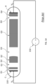
- FIG. 1A shows a simplified schematic view of a prior art (direct-current) DC plasma reaction chamber (110) that can be used in a DC plasma processing system.
- Biasing of the DC plasma reaction chamber (110) may be provided by a DC voltage source (150) coupled between an anode, A, and a cathode, C, of the DC plasma reaction chamber (110).
- a glow discharge (plasma) may be formed in the chamber (110) based on interaction of a gas and electrons of a current that flows between the anode, A, and the cathode, D. This in turn produces free ions and electrons in the chamber (110).
- the principle of operation of such DC plasma reaction chamber (110) is well known to a person skilled in the art and therefore related details are omitted in the present disclosure.
- the glow discharge formed in the chamber (110) may include glow regions (G1, G2, G3, G4) that emit significant light, and dark regions (D1, D2, D3, D4) that may not emit light. Such regions may represent different operating characteristics of the DC plasma reaction chamber (110), including, for example, temperature and electric potential.
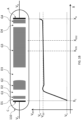
- FIG. 1B shows a graph representative of a variation in the (electric) potential, V PP , of the plasma along an axial direction (direction of longitudinal extension), X, of the chamber (110) during operation.
- the plasma potential, V PP varies from a value, Vc, that represents the potential applied to the cathode, C, by the DC voltage source (150 of FIG. 1A ), to a value, V A , that represents the potential applied to the anode, A, by the DC voltage source (150 of FIG. 1A ).
- V A is at zero volts (e.g., reference ground) and the value, Vc, is negative (e.g., in a range of about 0 (zero) - 500 volts).
- abrupt variation of the potential, V PP , in the regions (e.g., D1, G1, D2) close to the cathode, C, and in the regions (e.g., G4) close to the anode, A, may correspond to regions of higher operating temperatures of the chamber (110).
- the region G3, also known as the positive column is a region of quasi uniform/constant potential, V PP , and of lower operating temperature. For example, considering a segment [X G31 , X G32 ] along the axial direction, X, of the chamber (110) that as shown in FIG.
- V PP plasma potential across such segment [X G31 , X G32 ]
- the potential, V PP , across the segment [X G31 , X G32 ] may be considered as constant. Accordingly, as shown in FIG. 1B , the plasma potential, V PP , across the segment [X G31 , X G32 ] may be considered as equal to a value V G3 .
- the lower operating temperature and the constant potential value of the plasma in the positive column region, G3, allow use of such region for processing of substrates as shown in FIG. 1C and FIG. 1D .
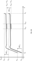
- FIG. 1C shows a simplified schematic view of a DC plasma processing system (100C) comprising a (substrate) stage, S, arranged in the positive column region, G3, of the DC plasma reaction chamber (110).
- the stage, S may be designed to support a flat substrate, and therefore may include a top flat/planar surface.
- the stage, S, shown in FIG. 1C is electrically isolated (not connected to any external electric potential) and therefore, and as known to a person skilled in the art, in the presence of the plasma potential, V PP , a potential, Vs, develops at the surface of the stage, S, that is referred to as the surface floating potential, V FP .
- FIG. 1C The relationship of the (surface) floating potential, V FP , to the plasma potential, V PP , is shown FIG. 1C .
- the plasma potential, Vpp, at a region [X G31 , X G32 ] of the chamber (110) where the stage, S, is arranged is equal to V G3
- the floating potential, V FP is lower than (negative with respect to) the plasma potential V G3 .
- the floating potential, V FP shown in the graph of FIG. 1C can be attributed to the "plasma sheath" that develops in the presence of the stage, S.
- a negative potential develops with respect to the bulk of the plasma. Consequently, an equilibrium potential drop develops between the bulk of the plasma and the wall or barrier.
- Such potential drop is confined to a small region of space next to the wall or barrier due to the charge imbalance that develops between the plasma and the wall or barrier.
- This layer of charge imbalance has a finite thickness, characterized by the Debye Length, and is called the "plasma sheath" or "sheath".
- the thickness of such a layer is several Debye lengths thick, a value whose size depends on various characteristics of the plasma. If the dimensions of the bulk plasma (e.g., chamber 110) are much greater than the Debye length, for example, then the Debye length depends on the plasma temperature and electron density. In the particular case of the DC plasma operating conditions supported by the teachings according to the present disclosure (e.g., EEMP system near room temperature to moderately above room temperature), the Debye length is in the order of several millimeters (e.g., less than 10 millimeters), and the difference between the potentials V G3 and V FP is in the order of several volts (e.g., less than 10 volts).
- the plasma sheath may develop in the presence of any wall or barrier, whether conductive or not. Accordingly, once a substrate (whether conductive or insulating) is placed atop the stage, S, the same floating potential, V FP , as described above with reference to FIG. 1C may develop at the surface of the substrate.
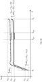
- FIG. 1D shows an exemplary biasing of the stage, S, of the DC plasma processing system of FIG. 1C via an external biasing signal generator (180) that is capacitively coupled to the stage, S, by a capacitor Cs.
- the potential, Va applied to the anode, A
- the potential, Va is at zero volts (e.g., coupled to the reference ground, Gnd).
- a biasing signal, V B applied to the stage, S, by the external biasing signal generator (180) may be referenced to the reference ground potential, Gnd.
- biasing signal, V B may be DC coupled to the stage, S
- teachings according to the present disclosure strictly prohibit such DC coupling to the stage so as to avoid a discharge path for a DC current through any intermediate points in the chamber (110), as such discharge path may substantially change operating conditions within the chamber (110).
- the biasing signal, V B may be used to control a potential (e.g., surface potential Vs) seen by free electrons and/or ions in the vicinity of the stage, S, or of the substrate when present. Accordingly, energy of the free electrons and/or ions may be controlled to levels required for processing of the substrate.
- a potential e.g., surface potential Vs
- the biasing signal, V B generated by the external biasing signal generator (e.g., 180 of FIG. 1D ) may start from zero and reach in a short period of time (represented by a leading edge slope) a voltage amplitude, V B1 .
- V B1 When the voltage amplitude, V B1 , is applied (e.g., AC coupled) to the stage, S, during a processing step (a) as shown in the top right-side graph of FIG. 1E , the voltage amplitude, V B1 , gets added (or subtracted if negative) to the surface floating potential, V FPa , to generate a surface potential, Vs, at the vicinity of the stage, S.
- V PPa because the free electrons and/or ions are at the plasma potential, V PPa , only a portion of the surface potential, Vs, that is above the plasma potential, V PPa , is seen by the free electrons and/or ions.
- Vs surface floating potential
- teachings according to the present disclosure either eliminate variations in the operating conditions within the chamber (e.g., 110 of FIG.
- variation in the operating conditions may be expected in view of different types of processing (e.g., (a) and (b) of FIG. 1E ) performed within the chamber (110), including for example, etching of a substrate with different reactive gasses, cleaning of a substrate or any other process that may alter and/or remove composition/material from the surface of the substrate.
- the different operating conditions for performing the different types of processing may further include corresponding variations and/or adjustments to any one of the DC plasma current, temperature, gas mixture or flow rate within the chamber (110).
- the kinetic energy of the free electrons and/or ions acquired through the application of the bias signal, V B , described above may accelerate the free electrons and/or ions towards the surface of the substrate and collide with the substrate to release the kinetic energy onto atoms at the surface of the substrate.
- Those atoms are at an energy level that is based on the potential within which they reside, or in other words, based on the floating potential, V FP .
- Various energy levels of one such atom for the processing type (a) described above with reference to FIG. 1E are shown in FIG.
- 1F including the energy level, E n , of a nucleus of an atom at the surface of the substrate, the energy level, E B , of an electron bound to the nucleus of an atom at the surface of the substrate, and the energy level, E e , of an electron at the orbit of an electron bound to a nucleus at the surface of the substrate.
- the energy level, E n of the nucleus is at the (negative) potential, V FPa
- the energy level, E e of the electron is at the (negative) potential (E n + E B ).
- an energy equal to, or greater than, the energy level, E e of the electron must be imparted onto the atom. Accordingly, considering a plasma processing only via the free electrons, the kinetic energy of the free electrons provided through application of the bias signal, V B , represented in FIG.
- V KEa (V B1 - ⁇ V FPa )
- E e (E n + E B )
- E n is based on the a priori unknown floating potential, V FPa
- precise control of the kinetic energy of the free electrons to precisely target the energy level, E e may not be possible.
- the floating potential (e.g., V FPa of FIG. 1F ) may be empirically and/or experimentally determined for a given process at stable operating conditions of the DC plasma chamber, any inconsistencies and/or lack of repeatability of such operating conditions may invalidate the determined floating potential.
- the task of precisely controlling the kinetic energy of the free electrons to exactly target the energy level of an atom at the surface of the substrate may not be feasible.
- some prior art implementations impart kinetic energies onto the atoms at the surface of the substrate that may be substantially larger than a target atom energy level, and therefore may not allow for selectivity (as atoms of different materials/compositions having different energy levels may equally be subjected to energy levels sufficient to break their orbital bonds).
- the electron enhanced material processing (EEMP) according to the teachings of the present disclosure overcome such shortcoming and therefore allow precise control of the kinetic energy of the free electrons to exactly and selectively target the energy level of an atom at the surface of the substrate.
- FIG. 2A shows a simplified schematic view of a DC plasma processing system (200A) according to an embodiment of the present invention comprising means (250, 260) to control the surface potential of the stage, S, when electrically isolated.
- the means (250, 260) allow for adjustment of the floating potential, V FP .
- the means (250, 260) include an adjustable DC voltage source (250) that is coupled to the anode, A, of the DC plasma reaction chamber (110), and a DC current source (260) that is coupled to the cathode, C, of the DC plasma reaction chamber (110).
- the potential, V A , of the anode, A may be controlled to be in a range from zero volts and upward (positive) with respect to the reference ground (Gnd at zero volts), and a (drain) current, Ip, that flows between the anode, A, and the cathode, C, through the reaction chamber (110) can be set by the DC current source (260).
- the potential, Vc, of the cathode, C is not forced by an external DC voltage source (e.g., 150 of FIG. 1D ), rather (is floating and) settles to a (negative) voltage that is based on the adjustable potential V A of the anode A, and the set current, Ip.
- Such configuration allows to independently control/adjust the floating potential, V FP , while maintaining the set current, Ip, through the reaction chamber (110) constant to establish and maintain a higher level of process stability and optimization.
- FIG. 2B shows two graphs representative of control of the surface potential, V FP , of the stage, S, for the DC plasma processing system (200A) described above with reference to FIG. 2A .
- FIG. 2B shows two graphs distinguished by use of solid or dashed lines, each representing the variation of the plasma potential, V PP , across the longitudinal extension, X, of the chamber (110) for two different voltages (Vai, V A2 ) applied to the anode, A, by the adjustable DC voltage source (250).
- Vai, V A2 the adjustable DC voltage source
- control of the anode, A, potential by the adjustable DC voltage source linearly affects the plasma potential, V PP , at any longitudinal coordinate, X, and therefore, linearly affects the floating potential, V FP , and the voltage, Vs, atop the stage, S,
- such linearity can be used in the EEMP system according to the present teachings to implement a closed loop control subsystem to automatically control the value of the floating potential, V FP , to a preset value (e.g., zero volts) while operating the DC plasma chamber for different types of material processing.
- FIG. 2C shows two graphs similar to the graphs described above with reference to FIG. 2B , including a specific case where the anode voltage, Vai, is equal to zero volts (solid lines).
- the floating potential volage for such case is equal to a negative value, V FP1 , and therefore negative with respect to (below) the plasma potential, V PP .
- +AV 13 (Vai - V FP1 )
- the floating potential can be adjusted to a value, V FP3 , that is equal to zero volts.
- such zeroing of the floating potential, V FP may allow precise control of the kinetic energy of free electrons in the DC plasma to exactly (and selectively) target energy levels of atoms at the surface of a substrate (whether conductive or insulating) being processed.
- the a priori unknown floating potential that determines the energy level, E n of a nucleus of an atom targeted/selected for processing is removed by zeroing of the floating potential, V FP .
- E n the energy level
- FIG. 3A shows a simplified schematic view of a DC plasma processing system (300A) according to an embodiment of the present disclosure comprising means (250, 260 of FIG. 2A ) to control a surface potential of the stage, S, and means (R, 311, V R of FIG. 3A ) to measure the surface potential, Vs (e.g., floating potential, V FP ) atop the stage.
- Vs e.g., floating potential, V FP
- the system (300A) represents an improvement over the system (200A) described above with reference to FIG. 2A by adding the means (R, 311, V R ) to measure the surface potential, Vs, or in other words, to measure the (surface) floating potential, V FP atop the stage.
- the means (R, 311, V R ) includes a reference plate, R, that is placed within DC plasma chamber (110) at a same (longitudinal coordinate) segment [X G31 , X G32 ] as the stage, S.
- the reference plate, R may be fabricated from any conductive material capable of withstanding (internal) operating conditions of the chamber (110), and may have any planar shape, including planar shapes according to, for example, a square, rectangle, circle, pentagon, trapezoid or other.
- the reference plate, R is arranged in the same region of the plate, S, and therefore in a region of a same substantially constant plasma potential, V PP , the reference plate, R, sees a same floating potential, V FP , as the stage, S.
- V FP floating potential
- An insulated conductive wire (311) attached to the reference plate, R may be used to route/couple the potential, V R , to measurement electronics (e.g., transducer) placed outside the chamber (110). It should be noted that such measurement electronics should not provide a DC current path to the plasma through plate R.
- placement of the reference plate, R may be at any longitudinal extension of the chamber (110) within the segment [X G31 , X G32 ] that is technically feasible and practical.
- the chamber, S may include an access door adjacent the stage, S, on one side of the chamber (110), in some exemplary embodiments the reference plate, R, may be arranged against, or in the vicinity, of a wall of the chamber (110) that is on an opposite side of the access door and stage, S.
- a center of the reference plate, R, and a center of the stage, S may be contained within a line that is perpendicular to the axial direction (e.g., centerline, direction of longitudinal extension) of the chamber (110).
- Applicants of the present disclosure have verified high accuracy of the means (R, 311, V R ) in tracking of the floating potential of the stage, S.
- FIG. 3B shows a simplified schematic view of a DC plasma processing system (300B) according to an embodiment of the present invention that is based on the system (300A) of FIG. 3A with added means (320, CT) for automatic control of the surface potential, V FP , at the stage, S.
- the means (320, CT) includes control electronics (320) configured to implement a closed loop control system to automatically control the value of the floating potential, V FP , at the stage, S, to a preset value (e.g., zero volts) while operating the DC plasma chamber for different types of processing.
- a preset value e.g., zero volts
- the control electronics (320) takes the (surface) potential, V R , of the reference plate, R, as input via a coupling provided by the insulated conductive wire (311), and generates therefrom a control (error) signal, CT, to the adjustable DC voltage source (250) to adjust the voltage, V A , provided to the anode, A, and therefore, as described above with reference to FIGs. 2A-2C , adjust the floating potential, V FP , at the stage, S.
- the control (error) signal, CT may be generated with respect to a desired target/preset value of the floating potential, V FP , such as, for example, zero volts.
- control electronics (320) A person skilled in the art is well aware of design techniques for implementing the control electronics (320) which are outside the scope of the present invention.
- a person skilled in the art is well aware of using operational amplifiers or error amplifiers in such control electronics (320), wherein inputs of such amplifiers may be coupled to the potential, V R , and to the desired target/preset value (e.g., zero volts) of the floating potential, V FP , to generate an error signal (e.g., CT) based on a difference of the inputs.
- V R the potential
- desired target/preset value e.g., zero volts
- V FP floating potential
- an error signal e.g., CT
- FIG. 4A shows a simplified schematic view of a DC plasma processing system (400A) according to an embodiment of the present invention that is based on the system of FIG. 3B with added biasing means (Cs, 480) for biasing of the stage, S.
- the biasing means (Cs, 480) includes a biasing signal generator (480) that is coupled to the stage, S, through a capacitor, Cs, of the biasing means.
- a biasing signal, V B generated at an output of the biasing signal generator (480) is capacitively coupled to the stage, S, through the capacitor, Cs.
- the biasing signal generator (480) may include, for example, a programmable waveform generator configured to output a waveform of the biasing signal, V B , according to desired characteristics, including for example, amplitude, frequency, duty cycle and/or rising/falling edges/slopes.
- the stage, S may include a first conductive portion (e.g., vertical lead connected to the capacitor Cs) for electrical coupling of the biasing signal, V B , to the stage, S, and a second portion of the stage (e.g., horizontal support plate) that may include conductive and/or insulating material.
- a first conductive portion e.g., vertical lead connected to the capacitor Cs
- a second portion of the stage e.g., horizontal support plate
- FIG. 4B shows an exemplary biasing signal, V B1 , provided to the stage, S, of the DC plasma processing system (400A) of FIG. 4A and a corresponding surface potential, Vs, generated at the surface of the stage, S.
- V B1 biasing signal
- Vs surface potential
- this allows a simple and straightforward generation of the biasing signal, V B1 , provided to the stage, S, for implementation of the electron enhanced material processing (EEMP) according to the teachings of the present disclosure that exactly and selectively targets the energy level of an atom (e.g., bound electron) at the surface of the substrate.
- EEMP electron enhanced material processing
- excitation of the energy levels of the atoms at the surface of the stage, S, or at the surface of a substrate arranged atop the stage, S may be primarily based on an instantaneous change in the surface potential, Vs. Accordingly, excitation of the energy levels may be accomplished immediately at the end of the transition of the biasing voltage to the target value, V B1 , or in other words, at the end of the slope shown in FIG. 4B .
- FIG. 4C shows exemplary energy levels of atoms at a surface of the stage, S, of the of the DC plasma processing system (400A) of FIG. 4A .
- FIG. 4C highlights benefits of the electron enhanced material processing (EEMP) according to the teachings of the present invention that allows adjustments to exactly and selectively target the energy level of an atom (e.g., Ee ⁇ V KE per FIG. 4C ) at the surface of the substrate based on the zeroing of the floating potential, V FP , according the above description with reference to FIGs. 2A-2C , further based on the reference plate, R, according to above description with reference to FIG.
- EEMP electron enhanced material processing
- FIG. 5 is a process chart (500) showing various steps of a method according to an embodiment of the present invention for processing a surface of a substrate.
- steps comprise: placing a substrate support stage in a region of a DC plasma reaction chamber configured to produce a positive column of the DC plasma, according to step (510); generating a DC plasma by coupling an adjustable DC voltage source and a DC current source respectively to an anode and a cathode of the DC plasma reaction chamber, according to step (520); based on the generating, producing a floating potential at a surface of the substrate support stage, according to step (530); adjusting a potential at the anode via the adjustable DC voltage source while maintaining via the DC current source a constant DC current between the anode and the cathode, according to step (540); and based on the adjusting and the maintaining, setting the floating potential to a potential of a reference ground of the adjustable DC voltage source, according to step (550).
Landscapes
- Physics & Mathematics (AREA)
- Engineering & Computer Science (AREA)
- Plasma & Fusion (AREA)
- Chemical & Material Sciences (AREA)
- Analytical Chemistry (AREA)
- Spectroscopy & Molecular Physics (AREA)
- Chemical Vapour Deposition (AREA)
- Drying Of Semiconductors (AREA)
- Plasma Technology (AREA)
Claims (19)
- Gleichstrom-Plasmasystem zur Verarbeitung eines Substrats, umfassend:eine Gleichstromplasmareaktionskammer (110), die so konfiguriert ist, dass sie ein Gleichstromplasma enthält, das zwischen einer Anode (A) und einer Kathode (C) der Gleichstromplasmareaktionskammer (110) erzeugt wird;eine einstellbare Gleichstromspannungsquelle (250) mit einem Ausgang, der elektrisch mit der Anode gekoppelt ist;Anode (A);eine Gleichstromquelle (260), die elektrisch mit der Kathode (C) gekoppelt ist; undein Substratstützgestell (S), das in einem Bereich der Gleichstromplasmareaktionskammer (110) angeordnet ist, die eine positive Säule des Gleichstromplasmas enthält,wobeidie einstellbare Gleichstromspannungsquelle (250) und die Gleichstromquelle (260) elektrisch mit einer Referenzmasse gekoppelt sind, unddie einstellbare Gleichstromspannungsquelle (250) so konfiguriert ist, dass sie während der Verarbeitung des Substrats ein elektrisches Potential an der Anode festsetzt, um ein schwebendes Potential an einer Oberfläche des Substratstützgestells (S) auf ein Potential der Referenzmasse einzustellen.
- Gleichstrom-Plasmasystem nach Anspruch 1, wobei:
die Gleichstromquelle konfiguriert ist, um während der Verarbeitung des Substrats einen konstanten Gleichstrom festzusetzen, der zwischen der Anode und der Kathode fließt, wobei der konstante Gleichstrom konfiguriert ist, um das Gleichstromplasma zu erzeugen. - Gleichstrom-Plasmasystem nach Anspruch 2, wobei:
das elektrische Potenzial an der Anode und der konstante Gleichstrom in Kombination ein Potenzial an der Kathode herstellen. - Gleichstrom-Plasmasystem nach Anspruch 2, wobei:
das elektrische Potenzial an der Anode unabhängig vom konstanten Gleichstrom einstellbar ist. - Gleichstrom-Plasmasystem nach einem der Ansprüche 1 bis 4, das zudem umfasst:
eine Referenzplatte aus einem leitfähigen Material, die in dem Bereich der Gleichstromplasmareaktionskammer angeordnet ist, die die positive Säule enthält, so dass ein Oberflächenpotenzial der Referenzplatte gleich dem schwebenden Potential ist. - Gleichstrom-Plasmasystem nach Anspruch 5, wobei:
das Substratstützgestell und die Referenzplatte innerhalb eines Segments entlang einer Längserstreckung der Gleichstromplasmareaktionskammer angeordnet sind. - Gleichstrom-Plasmasystem nach Anspruch 6, wobei:
eine Mitte des Substratstützgestells und eine Mitte der Referenzplatte innerhalb einer Linie enthalten sind, die senkrecht zu einer Richtung der Längserstreckung verläuft. - Gleichstrom-Plasmasystem nach einem der Ansprüche 5 bis 7, das zudem umfasst:eine Steuerelektronik, die über einen isolierenden, leitenden Draht elektrisch mit der Referenzplatte gekoppelt ist,wobeidie Steuerelektronik so konfiguriert ist, dass sie ein Fehlersignal auf Grundlage einer Differenz zwischen dem Oberflächenpotenzial der Referenzplatte und dem Potenzial der Referenzmasse erzeugt.
- Gleichstrom-Plasmasystem nach Anspruch 8, wobei:
die Steuerelektronik einen Operationsverstärker oder einen Fehlerverstärker umfasst. - Gleichstrom-Plasmasystem nach Anspruch 8, wobei:
die einstellbare Gleichstromspannungsquelle so konfiguriert ist, dass sie das Fehlersignal empfängt und das elektrische Potenzial an der Anode auf Grundlage eines Werts des Fehlersignals einstellt. - Gleichstrom-Plasmasystem nach Anspruch 10, wobei:
die einstellbare Gleichstromspannungsquelle, die Referenzplatte und die Steuerelektronik so konfiguriert sind, dass sie ein geschlossenes Regelsystem bereitstellen, um das schwebende Potenzial auf dem Potenzial der Referenzmasse aufrechtzuhalten. - Gleichstrom-Plasmasystem nach einem der Ansprüche 1 bis 11, das zudem umfasst:einen Vorspannungssignalgenerator, der kapazitiv mit dem Substratstützgestell gekoppelt ist, wobeider Vorspannungssignalgenerator so konfiguriert ist, dass er ein Vorspannungssignal mit einem Spannungsniveau erzeugt, der auf das Potential der Referenzmasse bezogen ist, wobei das Vorspannungssignal kapazitiv mit dem Substratstützgestell gekoppelt ist, unddas Vorspannungssignal so konfiguriert ist, dass es ein Oberflächenpotenzial des Substratstützgestells steuert.
- Gleichstrom-Plasmasystem nach Anspruch 12, wobei:
der Vorspannungssignalgenerator so konfiguriert ist, dass er die Wellenformcharakteristiken des Vorspannungssignals steuert, wobei die Wellenformcharakteristiken das Spannungsniveau, eine Frequenz, ein Tastverhältnis, eine steigende Flanke oder eine fallende Flanke umfassen. - Gleichstrom-Plasmasystem nach Anspruch 12, wobei:
wenn das Spannungsniveau des Vorspannungssignals null Volt beträgt, das Oberflächenpotential des Substratstützgestells bei null Volt liegt, das Energieniveau der freien Elektronen im Gleichstromplasma bei null Volt liegt und das Energieniveau der Atomkerne an einer Oberfläche des Substrats bei null Volt liegt. - Gleichstrom-Plasmasystem nach Anspruch 14, wobei:
wenn das Spannungsniveau des Vorspannungssignals um einen positiven Spannungsschritt erhöht wird, das Oberflächenpotential des Substratstützgestells um denselben positiven Spannungsschritt erhöht wird, das Energieniveau der freien Elektronen proportional zu dem positiven Spannungsschritt erhöht wird. - Gleichstrom-Plasmasystem nach Anspruch 15, wobei:
der positive Spannungsscritt während der Verarbeitung des Substrats wählbar ist, um das Energieniveau der freien Elektronen auf ein Energieniveau von an die Kerne gebundenen Elektronen zu erhöhen. - Verfahren zur Verarbeitung einer Oberfläche eines Substrats, wobei das Verfahren umfasst:
Verarbeiten des Substrats über das Gleichstrom-Plasmasystem nach einem der Ansprüche 1-16. - Verfahren zur Verarbeitung einer Oberfläche eines Substrats, wobei das Verfahren umfasst:Platzieren eines Substratstützgestells (S) in einem Bereich einer Gleichstromplasmareaktionskammer (110), die so konfiguriert ist, dass sie eine positive Säule von Gleichstromplasma erzeugt;Erzeugen des Gleichstromplasmas durch Koppeln einer einstellbaren Gleichstromspannungsquelle (250) und einer Gleichstromquelle (260) mit einer Anode (A) bzw. einer Kathode (C) der Gleichstromplasmareaktionskammer (110);auf Grundlage der Erzeugung, Produzieren eines schwebenden Potentials an der Oberfläche des Substratstützgestells (S);Einstellen eines Potentials an der Anode über die einstellbare Gleichstromspannungsquelle (250), während über die Gleichstromquelle (260) ein konstanter Gleichstrom zwischen der Anode (A) und der Kathode (C) aufrechterhalten wird; undauf Grundlage des Einstellens und des Aufrechthaltens, Festsetzen des schwebenden Potentials auf ein spezifisches Potential einer Referenzmasse der einstellbaren Gleichstromspannungsquelle (250).
- Verfahren nach Anspruch 18, ferner umfassend:Platzieren eines Substrats auf dem Substratstützgestell;kapazitives Koppeln eines Vorspannungssignals an das Substratstützgestell, wodurch freie Elektronen im Gleichstromplasma mit Strom versorgt werden;auf Grundlage der Stromversorgung, Beschleunigen der freien Elektronen auf eine Oberfläche des Substrats; undauf Grundlage der Beschleunigung, Kollidieren der freien Elektronen mit Atomen an der Oberfläche des Substrats, wodurch Energiebindungen zwischen Elektronen undAtomkernen aufbrechen,wobei ein Spannungsniveau des Vorspannungssignals so gewählt wird, dass ein spezifisches Energieniveau der Elektronen der Atome angestrebt wird, wobei die Atome ein spezifisches Material bilden.
Applications Claiming Priority (2)
| Application Number | Priority Date | Filing Date | Title |
|---|---|---|---|
| US17/524,330 US11664195B1 (en) | 2021-11-11 | 2021-11-11 | DC plasma control for electron enhanced material processing |
| PCT/US2022/078600 WO2023086731A1 (en) | 2021-11-11 | 2022-10-24 | Dc plasma control for electron enhanced material processing |
Publications (3)
| Publication Number | Publication Date |
|---|---|
| EP4388574A1 EP4388574A1 (de) | 2024-06-26 |
| EP4388574B1 true EP4388574B1 (de) | 2024-11-20 |
| EP4388574C0 EP4388574C0 (de) | 2024-11-20 |
Family
ID=84362862
Family Applications (1)
| Application Number | Title | Priority Date | Filing Date |
|---|---|---|---|
| EP22813027.4A Active EP4388574B1 (de) | 2021-11-11 | 2022-10-24 | Gleichstromplasmasteuerung für elektronenverstärkte materialverarbeitung |
Country Status (9)
| Country | Link |
|---|---|
| US (3) | US11664195B1 (de) |
| EP (1) | EP4388574B1 (de) |
| JP (1) | JP7624120B2 (de) |
| KR (1) | KR102764231B1 (de) |
| CN (1) | CN118355468B (de) |
| AU (1) | AU2022386575B2 (de) |
| MX (1) | MX2024003820A (de) |
| TW (1) | TWI835377B (de) |
| WO (1) | WO2023086731A1 (de) |
Families Citing this family (2)
| Publication number | Priority date | Publication date | Assignee | Title |
|---|---|---|---|---|
| US11688588B1 (en) * | 2022-02-09 | 2023-06-27 | Velvetch Llc | Electron bias control signals for electron enhanced material processing |
| US11869747B1 (en) | 2023-01-04 | 2024-01-09 | Velvetch Llc | Atomic layer etching by electron wavefront |
Family Cites Families (37)
| Publication number | Priority date | Publication date | Assignee | Title |
|---|---|---|---|---|
| US4464223A (en) | 1983-10-03 | 1984-08-07 | Tegal Corp. | Plasma reactor apparatus and method |
| US4756794A (en) | 1987-08-31 | 1988-07-12 | The United States Of America As Represented By The Secretary Of The Navy | Atomic layer etching |
| US5039376A (en) | 1989-09-19 | 1991-08-13 | Stefan Zukotynski | Method and apparatus for the plasma etching, substrate cleaning, or deposition of materials by D.C. glow discharge |
| JPH04226030A (ja) * | 1990-05-31 | 1992-08-14 | Matsushita Electric Ind Co Ltd | プラズマ表面処理方法およびプラズマ表面処理装置 |
| US5221416A (en) | 1990-05-31 | 1993-06-22 | Matsushita Electric Industrial Co., Ltd. | Plasma surface treating method |
| CH689767A5 (de) * | 1992-03-24 | 1999-10-15 | Balzers Hochvakuum | Verfahren zur Werkstueckbehandlung in einer Vakuumatmosphaere und Vakuumbehandlungsanlage. |
| US5882538A (en) * | 1995-08-28 | 1999-03-16 | Georgia Tech Research Corporation | Method and apparatus for low energy electron enhanced etching of substrates |
| US6027663A (en) | 1995-08-28 | 2000-02-22 | Georgia Tech Research Corporation | Method and apparatus for low energy electron enhanced etching of substrates |
| US6048435A (en) | 1996-07-03 | 2000-04-11 | Tegal Corporation | Plasma etch reactor and method for emerging films |
| US5917285A (en) | 1996-07-24 | 1999-06-29 | Georgia Tech Research Corporation | Apparatus and method for reducing operating voltage in gas discharge devices |
| US6258287B1 (en) | 1996-08-28 | 2001-07-10 | Georgia Tech Research Corporation | Method and apparatus for low energy electron enhanced etching of substrates in an AC or DC plasma environment |
| US6033587A (en) | 1996-09-20 | 2000-03-07 | Georgia Tech Research Corporation | Method and apparatus for low energy electron enhanced etching and cleaning of substrates in the positive column of a plasma |
| WO1998013531A1 (de) | 1996-09-23 | 1998-04-02 | Siemens Aktiengesellschaft | Verfahren und vorrichtung zur herstellung einer wärmedämmschicht |
| JP4607328B2 (ja) | 1998-12-03 | 2011-01-05 | ジョージア テック リサーチ コーポレイション | 基板の低エネルギー電子促進エッチング及びクリーニング方法及び装置 |
| JP2003504835A (ja) | 1998-12-03 | 2003-02-04 | ジョージア テック リサーチ コーポレイション | 基板の低エネルギー電子促進エッチング方法および装置 |
| US6306265B1 (en) * | 1999-02-12 | 2001-10-23 | Applied Materials, Inc. | High-density plasma for ionized metal deposition capable of exciting a plasma wave |
| DE19919832A1 (de) | 1999-04-30 | 2000-11-09 | Bosch Gmbh Robert | Verfahren zum anisotropen Plasmaätzen von Halbleitern |
| US6646386B1 (en) | 1999-07-20 | 2003-11-11 | Tokyo Electron Limited | Stabilized oscillator circuit for plasma density measurement |
| US6335536B1 (en) * | 1999-10-27 | 2002-01-01 | Varian Semiconductor Equipment Associates, Inc. | Method and apparatus for low voltage plasma doping using dual pulses |
| US6884717B1 (en) | 2002-01-03 | 2005-04-26 | The United States Of America As Represented By The Secretary Of The Air Force | Stiffened backside fabrication for microwave radio frequency wafers |
| AU2006223254B2 (en) | 2005-03-11 | 2012-04-26 | Perkinelmer U.S. Llc | Plasmas and methods of using them |
| US7777197B2 (en) | 2005-06-02 | 2010-08-17 | Applied Materials, Inc. | Vacuum reaction chamber with x-lamp heater |
| JP4838736B2 (ja) | 2007-01-25 | 2011-12-14 | 株式会社日立ハイテクノロジーズ | プラズマ処理装置 |
| JP4317888B2 (ja) | 2007-08-31 | 2009-08-19 | 富士フイルム株式会社 | スパッタ方法およびスパッタ装置 |
| WO2010008598A1 (en) * | 2008-07-17 | 2010-01-21 | Verity Instruments, Inc. | Electron beam exciter for use in chemical analysis in processing systems |
| JP5227734B2 (ja) | 2008-10-15 | 2013-07-03 | ジョージア テック リサーチ コーポレーション | 基板の低エネルギー電子促進エッチング及びクリーニング方法及び装置 |
| KR101380835B1 (ko) | 2011-07-22 | 2014-04-04 | 성균관대학교산학협력단 | 그래핀의 원자층 식각 방법 |
| US20130255717A1 (en) * | 2012-04-03 | 2013-10-03 | Kla-Tencor Corporation | System and method for cleaning surfaces and components of mask and wafer inspection systems based on the positive column of a glow discharge plasma |
| US9793098B2 (en) * | 2012-09-14 | 2017-10-17 | Vapor Technologies, Inc. | Low pressure arc plasma immersion coating vapor deposition and ion treatment |
| US9620382B2 (en) | 2013-12-06 | 2017-04-11 | University Of Maryland, College Park | Reactor for plasma-based atomic layer etching of materials |
| US10002744B2 (en) * | 2013-12-17 | 2018-06-19 | Tokyo Electron Limited | System and method for controlling plasma density |
| JP6532066B2 (ja) | 2015-03-30 | 2019-06-19 | 東京エレクトロン株式会社 | 原子層をエッチングする方法 |
| KR20170024922A (ko) | 2015-08-26 | 2017-03-08 | 삼성전자주식회사 | 플라즈마 발생 장치 |
| US10566212B2 (en) | 2016-12-19 | 2020-02-18 | Lam Research Corporation | Designer atomic layer etching |
| US10373804B2 (en) | 2017-02-03 | 2019-08-06 | Applied Materials, Inc. | System for tunable workpiece biasing in a plasma reactor |
| US10504742B2 (en) | 2017-05-31 | 2019-12-10 | Asm Ip Holding B.V. | Method of atomic layer etching using hydrogen plasma |
| US11404245B2 (en) | 2018-02-28 | 2022-08-02 | Taiwan Semiconductor Manufacturing Co., Ltd. | DC bias in plasma process |
-
2021
- 2021-11-11 US US17/524,330 patent/US11664195B1/en active Active
-
2022
- 2022-09-12 US US17/942,808 patent/US11715623B2/en active Active
- 2022-09-16 US US17/946,434 patent/US11676797B2/en active Active
- 2022-10-24 WO PCT/US2022/078600 patent/WO2023086731A1/en not_active Ceased
- 2022-10-24 AU AU2022386575A patent/AU2022386575B2/en active Active
- 2022-10-24 JP JP2024518981A patent/JP7624120B2/ja active Active
- 2022-10-24 KR KR1020247019329A patent/KR102764231B1/ko active Active
- 2022-10-24 MX MX2024003820A patent/MX2024003820A/es unknown
- 2022-10-24 CN CN202280074668.3A patent/CN118355468B/zh active Active
- 2022-10-24 EP EP22813027.4A patent/EP4388574B1/de active Active
- 2022-11-01 TW TW111141483A patent/TWI835377B/zh active
Also Published As
| Publication number | Publication date |
|---|---|
| US11676797B2 (en) | 2023-06-13 |
| TW202320121A (zh) | 2023-05-16 |
| KR102764231B1 (ko) | 2025-02-07 |
| AU2022386575B2 (en) | 2024-07-04 |
| AU2022386575A1 (en) | 2024-04-04 |
| JP2024545554A (ja) | 2024-12-10 |
| EP4388574A1 (de) | 2024-06-26 |
| WO2023086731A1 (en) | 2023-05-19 |
| KR20240096854A (ko) | 2024-06-26 |
| US20230144264A1 (en) | 2023-05-11 |
| EP4388574C0 (de) | 2024-11-20 |
| US20230140979A1 (en) | 2023-05-11 |
| US11715623B2 (en) | 2023-08-01 |
| TWI835377B (zh) | 2024-03-11 |
| CA3234154A1 (en) | 2023-05-19 |
| CN118355468A (zh) | 2024-07-16 |
| US20230143453A1 (en) | 2023-05-11 |
| CN118355468B (zh) | 2024-10-18 |
| US11664195B1 (en) | 2023-05-30 |
| MX2024003820A (es) | 2024-06-19 |
| JP7624120B2 (ja) | 2025-01-29 |
Similar Documents
| Publication | Publication Date | Title |
|---|---|---|
| EP4388574B1 (de) | Gleichstromplasmasteuerung für elektronenverstärkte materialverarbeitung | |
| US12125686B2 (en) | Electron bias control signals for electron enhanced material processing | |
| EP4569535B1 (de) | Atomlagenätzung durch elektronenwellenfront | |
| CA3234154C (en) | Dc plasma control for electron enhanced material processing | |
| CA3241149C (en) | Electron bias control signals for electron enhanced material processing | |
| US20240347323A1 (en) | Composite stage for electron enhanced material processing |
Legal Events
| Date | Code | Title | Description |
|---|---|---|---|
| STAA | Information on the status of an ep patent application or granted ep patent |
Free format text: STATUS: UNKNOWN |
|
| STAA | Information on the status of an ep patent application or granted ep patent |
Free format text: STATUS: THE INTERNATIONAL PUBLICATION HAS BEEN MADE |
|
| PUAI | Public reference made under article 153(3) epc to a published international application that has entered the european phase |
Free format text: ORIGINAL CODE: 0009012 |
|
| STAA | Information on the status of an ep patent application or granted ep patent |
Free format text: STATUS: REQUEST FOR EXAMINATION WAS MADE |
|
| GRAP | Despatch of communication of intention to grant a patent |
Free format text: ORIGINAL CODE: EPIDOSNIGR1 |
|
| STAA | Information on the status of an ep patent application or granted ep patent |
Free format text: STATUS: GRANT OF PATENT IS INTENDED |
|
| 17P | Request for examination filed |
Effective date: 20240318 |
|
| AK | Designated contracting states |
Kind code of ref document: A1 Designated state(s): AL AT BE BG CH CY CZ DE DK EE ES FI FR GB GR HR HU IE IS IT LI LT LU LV MC ME MK MT NL NO PL PT RO RS SE SI SK SM TR |
|
| INTG | Intention to grant announced |
Effective date: 20240620 |
|
| GRAS | Grant fee paid |
Free format text: ORIGINAL CODE: EPIDOSNIGR3 |
|
| GRAA | (expected) grant |
Free format text: ORIGINAL CODE: 0009210 |
|
| STAA | Information on the status of an ep patent application or granted ep patent |
Free format text: STATUS: THE PATENT HAS BEEN GRANTED |
|
| DAV | Request for validation of the european patent (deleted) | ||
| DAX | Request for extension of the european patent (deleted) | ||
| AK | Designated contracting states |
Kind code of ref document: B1 Designated state(s): AL AT BE BG CH CY CZ DE DK EE ES FI FR GB GR HR HU IE IS IT LI LT LU LV MC ME MK MT NL NO PL PT RO RS SE SI SK SM TR |
|
| REG | Reference to a national code |
Ref country code: GB Ref legal event code: FG4D |
|
| REG | Reference to a national code |
Ref country code: CH Ref legal event code: EP |
|
| REG | Reference to a national code |
Ref country code: DE Ref legal event code: R096 Ref document number: 602022008006 Country of ref document: DE |
|
| REG | Reference to a national code |
Ref country code: IE Ref legal event code: FG4D |
|
| U01 | Request for unitary effect filed |
Effective date: 20241121 |
|
| U07 | Unitary effect registered |
Designated state(s): AT BE BG DE DK EE FI FR IT LT LU LV MT NL PT RO SE SI Effective date: 20241127 |
|
| PG25 | Lapsed in a contracting state [announced via postgrant information from national office to epo] |
Ref country code: HR Free format text: LAPSE BECAUSE OF FAILURE TO SUBMIT A TRANSLATION OF THE DESCRIPTION OR TO PAY THE FEE WITHIN THE PRESCRIBED TIME-LIMIT Effective date: 20241120 Ref country code: IS Free format text: LAPSE BECAUSE OF FAILURE TO SUBMIT A TRANSLATION OF THE DESCRIPTION OR TO PAY THE FEE WITHIN THE PRESCRIBED TIME-LIMIT Effective date: 20250320 |
|
| PG25 | Lapsed in a contracting state [announced via postgrant information from national office to epo] |
Ref country code: ES Free format text: LAPSE BECAUSE OF FAILURE TO SUBMIT A TRANSLATION OF THE DESCRIPTION OR TO PAY THE FEE WITHIN THE PRESCRIBED TIME-LIMIT Effective date: 20241120 |
|
| PG25 | Lapsed in a contracting state [announced via postgrant information from national office to epo] |
Ref country code: NO Free format text: LAPSE BECAUSE OF FAILURE TO SUBMIT A TRANSLATION OF THE DESCRIPTION OR TO PAY THE FEE WITHIN THE PRESCRIBED TIME-LIMIT Effective date: 20250220 |
|
| PG25 | Lapsed in a contracting state [announced via postgrant information from national office to epo] |
Ref country code: GR Free format text: LAPSE BECAUSE OF FAILURE TO SUBMIT A TRANSLATION OF THE DESCRIPTION OR TO PAY THE FEE WITHIN THE PRESCRIBED TIME-LIMIT Effective date: 20250221 |
|
| PG25 | Lapsed in a contracting state [announced via postgrant information from national office to epo] |
Ref country code: PL Free format text: LAPSE BECAUSE OF FAILURE TO SUBMIT A TRANSLATION OF THE DESCRIPTION OR TO PAY THE FEE WITHIN THE PRESCRIBED TIME-LIMIT Effective date: 20241120 |
|
| PG25 | Lapsed in a contracting state [announced via postgrant information from national office to epo] |
Ref country code: RS Free format text: LAPSE BECAUSE OF FAILURE TO SUBMIT A TRANSLATION OF THE DESCRIPTION OR TO PAY THE FEE WITHIN THE PRESCRIBED TIME-LIMIT Effective date: 20250220 |
|
| PG25 | Lapsed in a contracting state [announced via postgrant information from national office to epo] |
Ref country code: SM Free format text: LAPSE BECAUSE OF FAILURE TO SUBMIT A TRANSLATION OF THE DESCRIPTION OR TO PAY THE FEE WITHIN THE PRESCRIBED TIME-LIMIT Effective date: 20241120 |
|
| PG25 | Lapsed in a contracting state [announced via postgrant information from national office to epo] |
Ref country code: SK Free format text: LAPSE BECAUSE OF FAILURE TO SUBMIT A TRANSLATION OF THE DESCRIPTION OR TO PAY THE FEE WITHIN THE PRESCRIBED TIME-LIMIT Effective date: 20241120 |
|
| PG25 | Lapsed in a contracting state [announced via postgrant information from national office to epo] |
Ref country code: CZ Free format text: LAPSE BECAUSE OF FAILURE TO SUBMIT A TRANSLATION OF THE DESCRIPTION OR TO PAY THE FEE WITHIN THE PRESCRIBED TIME-LIMIT Effective date: 20241120 |
|
| PLBE | No opposition filed within time limit |
Free format text: ORIGINAL CODE: 0009261 |
|
| STAA | Information on the status of an ep patent application or granted ep patent |
Free format text: STATUS: NO OPPOSITION FILED WITHIN TIME LIMIT |
|
| 26N | No opposition filed |
Effective date: 20250821 |
|
| REG | Reference to a national code |
Ref country code: CH Ref legal event code: U11 Free format text: ST27 STATUS EVENT CODE: U-0-0-U10-U11 (AS PROVIDED BY THE NATIONAL OFFICE) Effective date: 20251101 |
|
| U20 | Renewal fee for the european patent with unitary effect paid |
Year of fee payment: 4 Effective date: 20251027 |
|
| PGFP | Annual fee paid to national office [announced via postgrant information from national office to epo] |
Ref country code: CH Payment date: 20251101 Year of fee payment: 4 |