EP4386473A1 - Magnetooptischer dünnfilm, optischer isolator und verfahren zur herstellung eines magnetooptischen dünnfilms - Google Patents
Magnetooptischer dünnfilm, optischer isolator und verfahren zur herstellung eines magnetooptischen dünnfilms Download PDFInfo
- Publication number
- EP4386473A1 EP4386473A1 EP22863532.2A EP22863532A EP4386473A1 EP 4386473 A1 EP4386473 A1 EP 4386473A1 EP 22863532 A EP22863532 A EP 22863532A EP 4386473 A1 EP4386473 A1 EP 4386473A1
- Authority
- EP
- European Patent Office
- Prior art keywords
- thin film
- magneto
- diffusion barrier
- barrier layer
- optic thin
- Prior art date
- Legal status (The legal status is an assumption and is not a legal conclusion. Google has not performed a legal analysis and makes no representation as to the accuracy of the status listed.)
- Pending
Links
- 239000010409 thin film Substances 0.000 title claims abstract description 107
- 230000003287 optical effect Effects 0.000 title claims abstract description 57
- 238000000034 method Methods 0.000 title claims abstract description 18
- 238000004519 manufacturing process Methods 0.000 title claims abstract description 8
- 238000009792 diffusion process Methods 0.000 claims abstract description 105
- 230000004888 barrier function Effects 0.000 claims abstract description 100
- 239000000758 substrate Substances 0.000 claims abstract description 41
- 229910044991 metal oxide Inorganic materials 0.000 claims abstract description 17
- 150000004706 metal oxides Chemical class 0.000 claims abstract description 17
- 238000002955 isolation Methods 0.000 claims abstract description 16
- 239000000395 magnesium oxide Substances 0.000 claims description 58
- CPLXHLVBOLITMK-UHFFFAOYSA-N magnesium oxide Inorganic materials [Mg]=O CPLXHLVBOLITMK-UHFFFAOYSA-N 0.000 claims description 58
- AXZKOIWUVFPNLO-UHFFFAOYSA-N magnesium;oxygen(2-) Chemical compound [O-2].[Mg+2] AXZKOIWUVFPNLO-UHFFFAOYSA-N 0.000 claims description 58
- XLOMVQKBTHCTTD-UHFFFAOYSA-N Zinc monoxide Chemical compound [Zn]=O XLOMVQKBTHCTTD-UHFFFAOYSA-N 0.000 claims description 17
- XUIMIQQOPSSXEZ-UHFFFAOYSA-N Silicon Chemical compound [Si] XUIMIQQOPSSXEZ-UHFFFAOYSA-N 0.000 claims description 15
- 239000002223 garnet Substances 0.000 claims description 15
- MTRJKZUDDJZTLA-UHFFFAOYSA-N iron yttrium Chemical compound [Fe].[Y] MTRJKZUDDJZTLA-UHFFFAOYSA-N 0.000 claims description 15
- 229910052710 silicon Inorganic materials 0.000 claims description 15
- 239000010703 silicon Substances 0.000 claims description 15
- 238000000151 deposition Methods 0.000 claims description 13
- 229910052581 Si3N4 Inorganic materials 0.000 claims description 12
- QVGXLLKOCUKJST-UHFFFAOYSA-N atomic oxygen Chemical compound [O] QVGXLLKOCUKJST-UHFFFAOYSA-N 0.000 claims description 12
- 229910052760 oxygen Inorganic materials 0.000 claims description 12
- 239000001301 oxygen Substances 0.000 claims description 12
- HQVNEWCFYHHQES-UHFFFAOYSA-N silicon nitride Chemical compound N12[Si]34N5[Si]62N3[Si]51N64 HQVNEWCFYHHQES-UHFFFAOYSA-N 0.000 claims description 12
- 230000008021 deposition Effects 0.000 claims description 6
- 239000010408 film Substances 0.000 claims description 6
- 239000012212 insulator Substances 0.000 claims description 6
- 238000000137 annealing Methods 0.000 claims description 3
- 238000001816 cooling Methods 0.000 claims description 3
- 238000011065 in-situ storage Methods 0.000 claims description 3
- 230000000694 effects Effects 0.000 abstract description 11
- 230000006911 nucleation Effects 0.000 abstract description 8
- 238000010899 nucleation Methods 0.000 abstract description 8
- 239000000463 material Substances 0.000 description 26
- VYPSYNLAJGMNEJ-UHFFFAOYSA-N Silicium dioxide Chemical compound O=[Si]=O VYPSYNLAJGMNEJ-UHFFFAOYSA-N 0.000 description 12
- 239000004065 semiconductor Substances 0.000 description 11
- 230000032683 aging Effects 0.000 description 8
- 238000012360 testing method Methods 0.000 description 8
- 238000002834 transmittance Methods 0.000 description 8
- 230000008033 biological extinction Effects 0.000 description 7
- 239000000377 silicon dioxide Substances 0.000 description 6
- 239000011787 zinc oxide Substances 0.000 description 6
- 238000010586 diagram Methods 0.000 description 4
- 230000005415 magnetization Effects 0.000 description 4
- 239000000382 optic material Substances 0.000 description 4
- 238000002360 preparation method Methods 0.000 description 4
- -1 cerium ions Chemical class 0.000 description 3
- 238000009826 distribution Methods 0.000 description 3
- 238000005516 engineering process Methods 0.000 description 3
- 238000002474 experimental method Methods 0.000 description 3
- 230000010355 oscillation Effects 0.000 description 3
- 230000008569 process Effects 0.000 description 3
- 239000013077 target material Substances 0.000 description 3
- 238000002441 X-ray diffraction Methods 0.000 description 2
- 230000015556 catabolic process Effects 0.000 description 2
- 238000004891 communication Methods 0.000 description 2
- 238000002425 crystallisation Methods 0.000 description 2
- 230000008025 crystallization Effects 0.000 description 2
- 238000006731 degradation reaction Methods 0.000 description 2
- 238000011160 research Methods 0.000 description 2
- 229910052684 Cerium Inorganic materials 0.000 description 1
- 238000005352 clarification Methods 0.000 description 1
- 239000013078 crystal Substances 0.000 description 1
- 238000011161 development Methods 0.000 description 1
- 230000018109 developmental process Effects 0.000 description 1
- 239000012535 impurity Substances 0.000 description 1
- 230000010354 integration Effects 0.000 description 1
- 150000002500 ions Chemical class 0.000 description 1
- 230000007246 mechanism Effects 0.000 description 1
- 150000002736 metal compounds Chemical class 0.000 description 1
- 238000012986 modification Methods 0.000 description 1
- 230000004048 modification Effects 0.000 description 1
- 229910052761 rare earth metal Inorganic materials 0.000 description 1
- 235000012239 silicon dioxide Nutrition 0.000 description 1
- 230000035882 stress Effects 0.000 description 1
- 230000003746 surface roughness Effects 0.000 description 1
- 230000008646 thermal stress Effects 0.000 description 1
Images


Classifications
-
- G—PHYSICS
- G02—OPTICS
- G02F—OPTICAL DEVICES OR ARRANGEMENTS FOR THE CONTROL OF LIGHT BY MODIFICATION OF THE OPTICAL PROPERTIES OF THE MEDIA OF THE ELEMENTS INVOLVED THEREIN; NON-LINEAR OPTICS; FREQUENCY-CHANGING OF LIGHT; OPTICAL LOGIC ELEMENTS; OPTICAL ANALOGUE/DIGITAL CONVERTERS
- G02F1/00—Devices or arrangements for the control of the intensity, colour, phase, polarisation or direction of light arriving from an independent light source, e.g. switching, gating or modulating; Non-linear optics
- G02F1/01—Devices or arrangements for the control of the intensity, colour, phase, polarisation or direction of light arriving from an independent light source, e.g. switching, gating or modulating; Non-linear optics for the control of the intensity, phase, polarisation or colour
- G02F1/09—Devices or arrangements for the control of the intensity, colour, phase, polarisation or direction of light arriving from an independent light source, e.g. switching, gating or modulating; Non-linear optics for the control of the intensity, phase, polarisation or colour based on magneto-optical elements, e.g. exhibiting Faraday effect
- G02F1/093—Devices or arrangements for the control of the intensity, colour, phase, polarisation or direction of light arriving from an independent light source, e.g. switching, gating or modulating; Non-linear optics for the control of the intensity, phase, polarisation or colour based on magneto-optical elements, e.g. exhibiting Faraday effect used as non-reciprocal devices, e.g. optical isolators, circulators
-
- G—PHYSICS
- G02—OPTICS
- G02F—OPTICAL DEVICES OR ARRANGEMENTS FOR THE CONTROL OF LIGHT BY MODIFICATION OF THE OPTICAL PROPERTIES OF THE MEDIA OF THE ELEMENTS INVOLVED THEREIN; NON-LINEAR OPTICS; FREQUENCY-CHANGING OF LIGHT; OPTICAL LOGIC ELEMENTS; OPTICAL ANALOGUE/DIGITAL CONVERTERS
- G02F1/00—Devices or arrangements for the control of the intensity, colour, phase, polarisation or direction of light arriving from an independent light source, e.g. switching, gating or modulating; Non-linear optics
- G02F1/01—Devices or arrangements for the control of the intensity, colour, phase, polarisation or direction of light arriving from an independent light source, e.g. switching, gating or modulating; Non-linear optics for the control of the intensity, phase, polarisation or colour
- G02F1/09—Devices or arrangements for the control of the intensity, colour, phase, polarisation or direction of light arriving from an independent light source, e.g. switching, gating or modulating; Non-linear optics for the control of the intensity, phase, polarisation or colour based on magneto-optical elements, e.g. exhibiting Faraday effect
-
- C—CHEMISTRY; METALLURGY
- C30—CRYSTAL GROWTH
- C30B—SINGLE-CRYSTAL GROWTH; UNIDIRECTIONAL SOLIDIFICATION OF EUTECTIC MATERIAL OR UNIDIRECTIONAL DEMIXING OF EUTECTOID MATERIAL; REFINING BY ZONE-MELTING OF MATERIAL; PRODUCTION OF A HOMOGENEOUS POLYCRYSTALLINE MATERIAL WITH DEFINED STRUCTURE; SINGLE CRYSTALS OR HOMOGENEOUS POLYCRYSTALLINE MATERIAL WITH DEFINED STRUCTURE; AFTER-TREATMENT OF SINGLE CRYSTALS OR A HOMOGENEOUS POLYCRYSTALLINE MATERIAL WITH DEFINED STRUCTURE; APPARATUS THEREFOR
- C30B25/00—Single-crystal growth by chemical reaction of reactive gases, e.g. chemical vapour-deposition growth
- C30B25/02—Epitaxial-layer growth
- C30B25/18—Epitaxial-layer growth characterised by the substrate
- C30B25/183—Epitaxial-layer growth characterised by the substrate being provided with a buffer layer, e.g. a lattice matching layer
-
- C—CHEMISTRY; METALLURGY
- C30—CRYSTAL GROWTH
- C30B—SINGLE-CRYSTAL GROWTH; UNIDIRECTIONAL SOLIDIFICATION OF EUTECTIC MATERIAL OR UNIDIRECTIONAL DEMIXING OF EUTECTOID MATERIAL; REFINING BY ZONE-MELTING OF MATERIAL; PRODUCTION OF A HOMOGENEOUS POLYCRYSTALLINE MATERIAL WITH DEFINED STRUCTURE; SINGLE CRYSTALS OR HOMOGENEOUS POLYCRYSTALLINE MATERIAL WITH DEFINED STRUCTURE; AFTER-TREATMENT OF SINGLE CRYSTALS OR A HOMOGENEOUS POLYCRYSTALLINE MATERIAL WITH DEFINED STRUCTURE; APPARATUS THEREFOR
- C30B28/00—Production of homogeneous polycrystalline material with defined structure
- C30B28/12—Production of homogeneous polycrystalline material with defined structure directly from the gas state
-
- C—CHEMISTRY; METALLURGY
- C30—CRYSTAL GROWTH
- C30B—SINGLE-CRYSTAL GROWTH; UNIDIRECTIONAL SOLIDIFICATION OF EUTECTIC MATERIAL OR UNIDIRECTIONAL DEMIXING OF EUTECTOID MATERIAL; REFINING BY ZONE-MELTING OF MATERIAL; PRODUCTION OF A HOMOGENEOUS POLYCRYSTALLINE MATERIAL WITH DEFINED STRUCTURE; SINGLE CRYSTALS OR HOMOGENEOUS POLYCRYSTALLINE MATERIAL WITH DEFINED STRUCTURE; AFTER-TREATMENT OF SINGLE CRYSTALS OR A HOMOGENEOUS POLYCRYSTALLINE MATERIAL WITH DEFINED STRUCTURE; APPARATUS THEREFOR
- C30B29/00—Single crystals or homogeneous polycrystalline material with defined structure characterised by the material or by their shape
- C30B29/10—Inorganic compounds or compositions
- C30B29/16—Oxides
- C30B29/22—Complex oxides
- C30B29/28—Complex oxides with formula A3Me5O12 wherein A is a rare earth metal and Me is Fe, Ga, Sc, Cr, Co or Al, e.g. garnets
-
- G—PHYSICS
- G02—OPTICS
- G02F—OPTICAL DEVICES OR ARRANGEMENTS FOR THE CONTROL OF LIGHT BY MODIFICATION OF THE OPTICAL PROPERTIES OF THE MEDIA OF THE ELEMENTS INVOLVED THEREIN; NON-LINEAR OPTICS; FREQUENCY-CHANGING OF LIGHT; OPTICAL LOGIC ELEMENTS; OPTICAL ANALOGUE/DIGITAL CONVERTERS
- G02F1/00—Devices or arrangements for the control of the intensity, colour, phase, polarisation or direction of light arriving from an independent light source, e.g. switching, gating or modulating; Non-linear optics
- G02F1/0009—Materials therefor
- G02F1/0036—Magneto-optical materials
Definitions
- Embodiments of this application relate to the field of magneto-optic thin film material technologies, and more specifically, to a magneto-optic thin film, an optical isolator, and a method for manufacturing a magneto-optic thin film.
- a yttrium iron garnet (YIG) magneto-optic material has a high optical rotation coefficient, high saturation magnetization intensity, a large Faraday rotation angle, and the like, and is currently a main magneto-optic material for implementing an optical isolation function in the optical isolator.
- YIG yttrium iron garnet
- the YIG material is doped with rare earth elements (for example, doped with cerium ions Ce 3+ ), so that magneto-optic performance can be further improved.
- the substrate includes at least one of silicon (Si), silicon-on-insulator (SOI), and silicon nitride (SiN).
- the buffer layer includes yttrium iron garnet (YIG).
- YIG yttrium iron garnet
- the rare earth-doped yttrium iron garnet includes cerium-doped yttrium iron garnet (Ce:YIG).
- an optical isolator including the magneto-optic thin film according to the first aspect of this application.
- a method for manufacturing a magneto-optic thin film includes: step 1: depositing a diffusion barrier layer on a substrate, where the diffusion barrier layer includes a metal oxide; step 2: depositing a buffer layer including yttrium iron garnet (YIG) on the diffusion barrier layer; step 3: placing the film layer obtained in step 2 in a deposition cavity for in-situ annealing, injecting oxygen with an atmospheric pressure of 0.01 Pa to 10 Pa, increasing temperature to 600°C to 800°C, holding the temperature for 3 to 5 minutes, and waiting for natural cooling to room temperature; and step 4: placing the film layer obtained in step 3 at 650°C to 700°C in an oxygen atmosphere in which partial pressure of oxygen is 0 mTorr to 100 mTorr, and depositing an optical isolation layer including cerium-doped yttrium iron garnet (Ce:YIG) to obtain the magneto-optic thin film.
- step 1 depositing a diffusion barrier layer on a substrate, where the diffusion barrier layer includes a metal
- the metal oxide includes at least one of (MgO) and zinc oxide (ZnO).
- a thickness of the diffusion barrier layer is less than 10 nm.
- the thickness of the diffusion barrier layer is within a range of 3 nm to 8 nm.
- the substrate includes at least one of silicon (Si), silicon-on-insulator (SOI), and silicon nitride (SiN).
- a thickness of the buffer layer is within a range of 90 nm to 110 nm.
- A/B may indicate A or B.
- the term "and/or” in this specification describes only an association relationship between associated objects, and indicates that three relationships may exist.
- a and/or B may indicate the following three cases: Only A exists, both A and B exist, and only B exists.
- orientation terms such as “center”, “front”, “rear”, “inside”, and “outside” are defined relative to orientations or positions of components shown in the accompanying drawings. It should be understood that these directional terms are relative concepts and are used for relative description and clarification, but not to indicate or imply that an indicated apparatus or component needs to have a specific orientation or be constructed or operated in a specified orientation. The terms may vary correspondingly based on changes of the orientations in which the components in the accompanying drawings are placed, and therefore cannot be construed as a limitation on this application.
- a same reference numeral indicates a same component or a same part.
- only one part or component marked with a reference numeral may be used as an example in the figures. It should be understood that the reference numeral is also applicable to another same part or component.
- a cerium-doped yttrium iron garnet (Ce:YIG) thin film prepared by using a YIG thin film as a seed layer varies greatly with different processes, and loss of an obtained magneto-optic material is quite high, and may be higher than 20 dB.
- Direct deposition of the YIG/Ce:YIG thin film on a silicon substrate mainly has the following problems: (1) Because the YIG seed layer is in direct contact with the silicon substrate, magneto-optic performance and optical loss of the seed layer greatly affect performance of an entire device.
- a YIG thin film with a thickness of approximately 20 nanometers is usually used as a seed layer for growing a Ce:YIG thin film.
- a diffusion barrier layer including a metal oxide layer is deposited on a substrate to prevent mutual diffusion between a subsequently grown YIG layer and Ce:YIG and the substrate, so as to reduce optical loss and further improve crystallinity of the YIG layer and isolation performance of a magneto-optic thin film.
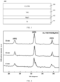
- FIG. 1 is a schematic diagram of a magneto-optic thin film 100 according to an embodiment of this application.
- the magneto-optic thin film 100 described herein includes a substrate 101, a diffusion barrier layer 102 disposed on the substrate 101, a buffer layer 103 disposed on the diffusion barrier layer 102, and an optical isolation layer 104 disposed on the buffer layer 103.
- the substrate 101 is made of silicon
- the diffusion barrier layer 102 is made of MgO
- the buffer layer 103 is made of YIG
- the optical isolation layer 104 is made of Ce:YIG.
- the optical isolation layer 104 made of the Ce:YIG is configured to isolate light through magneto-optic effect, so that light can be transmitted in the substrate 104 only unidirectionally.
- the buffer layer 103 made of the YIG is configured to alleviate lattice mismatch and thermal mismatch problems between the Ce:YIG and the substrate 101.
- the diffusion barrier layer 102 made of the MgO is configured to prevent mutual diffusion between the substrate 101, the buffer layer 103, and the optical isolation layer 104.
- the MgO compared with the SiO 2 , the MgO has higher density and thermal stability, and therefore can provide stable and reliable diffusion barrier effect. This further reduces optical loss of the magneto-optic thin film.
- a thickness of the diffusion barrier layer 102 may be less than 10 nm, for example, within a range of 3 nm to 8 nm, for example, 3 nm, 6 nm, or 8 nm. It should be understood that, in this embodiment of this application, the diffusion barrier layer 102 may have a larger or smaller thickness. This is not strictly limited in the scope of this application.
- loss of a YIG thin film material in the deposited buffer layer 103 can be adjusted by adjusting a thickness of the YIG thin film material.
- the inventor finds that the scattering loss of the material is low when a thickness of the buffer layer 103 is within a range of 90 nm to 110 nm.
- a layer of MgO is deposited on the substrate 101 as the diffusion barrier layer 102, to prevent mutual diffusion between the subsequently grown YIG and Ce:YIG thin film materials and the Si in the substrate 101, without affecting crystallinity of the YIG and Ce:YIG materials or mode field distribution of the device.
- loss can be reduced by selecting a buffer layer 103 that includes YIG and that has a thickness of 90 nm to 110 nm. In this manner, the finally prepared magneto-optic thin film 100 can achieve maximum saturation magnetization intensity of approximately 110 emu/cm 3 .
- a Faraday rotation angle of a target material with a doping concentration X of 2 is approximately 4300°/cm. This greatly helps improve a magneto-optic figure of merit of a material and develop a low-loss silicon-based optical isolator.
- the substrate 101 including the silicon is used as an example to describe the principle of this application.
- the substrate 101 may include another substrate material that is known or is available in the future, for example, silicon-on-insulator (SOI) or silicon nitride (SiN).
- the substrate 101 may include only one substrate material, or may include a plurality of substrate materials. This is not strictly limited in the scope of this application.
- a metal oxide in the diffusion barrier layer 102 may include zinc oxide (ZnO), instead of the MgO. Similar to the MgO, the deposited ZnO is polycrystalline. Therefore, this is more conducive to nucleation of the YIG on the diffusion barrier layer 102, and crystallinity is good. In addition, compared with the SiO 2 , the ZnO has higher density and thermal stability, and therefore can provide stable and reliable diffusion barrier effect. This further reduces optical loss of the magneto-optic thin film.
- ZnO zinc oxide
- the metal oxide in the diffusion barrier layer 102 may include both MgO and ZnO, instead of only the MgO or the ZnO. This also facilitates nucleation of the YIG on the diffusion barrier layer 102, and can provide stable and reliable diffusion barrier effect, and reduce optical loss of the magneto-optic thin film.
- the diffusion barrier layer 102 may include another metal compound with high density and thermal stability. This also facilitates nucleation of the YIG on the diffusion barrier layer 102, and can provide stable and reliable diffusion barrier effect, and reduce optical loss of the magneto-optic thin film.
- the buffer layer 103 including the YIG is used as an example to describe the principle of this application.
- the buffer layer 103 may include another buffer layer material that is known or that is available in the future. This is not strictly limited in the scope of this application.
- the optical isolation layer 104 including the Ce:YIG is used as an example to describe a principle of this application.
- the optical isolation layer 104 may include other rare earth-doped yttrium iron garnet. This is not strictly limited in the scope of this application.
- the magneto-optic thin film 100 described in this embodiment of this application may be used in an optical isolator, so that light can be transmitted in the optical isolator only along a single direction.
- An embodiment of this application further provides a method for manufacturing a magneto-optic thin film, including the following steps: Step 1: Deposit a diffusion barrier layer on a substrate, where the diffusion barrier layer includes a metal oxide, for example, MgO and/or ZnO, or another material, and is intended to prevent mutual diffusion between the subsequently grown YIG and Ce:YIG and the substrate, without affecting crystallinity of YIG and Ce:YIG materials or mode field distribution of a device. Step 2: Deposit a buffer layer including YIG on the diffusion barrier layer, where a thickness of the buffer layer is, for example, within a range of 90 nm to 110 nm.
- Step 1 Deposit a diffusion barrier layer on a substrate, where the diffusion barrier layer includes a metal oxide, for example, MgO and/or ZnO, or another material, and is intended to prevent mutual diffusion between the subsequently grown YIG and Ce:YIG and the substrate, without affecting crystallinity of YIG and Ce:YIG materials or mode field distribution of
- Step 3 Place the film layer obtained in step 2 in a deposition cavity for in-situ annealing, inject oxygen with an atmospheric pressure of 0.01 Pa to 10 Pa (for example, 0.01 Pa, 0.1Pa, or 10Pa), increase temperature to 600°C to 800°C, hold the temperature for 3 to 5 minutes, and wait for natural cooling to room temperature.
- Step 4 Place the film layer obtained in step 3 at 650°C to 700°C in an oxygen atmosphere in which partial pressure of oxygen is 0 mTorr to 100 mTorr, and deposit an optical isolation layer including Ce:YIG to obtain a magneto-optic thin film.
- step 4 a reason for preparation by using different partial pressure of oxygen is as follows: At low partial pressure of oxygen, there are many Fe 2+ ions in the Ce:YIG thin film, and material loss is high; and at high partial pressure of oxygen, Ce 3+ ions in the Ce:YIG thin film are oxidized into Ce 4+ , magneto-optic effect of the thin film is degraded, a device length increases, and loss increases.
- the MgO or the like is used as the diffusion barrier layer. This can improve crystallinity of a subsequently deposited thin film, and can also alleviate thermal stress mismatch, to prevent performance degradation due to stress mismatch between the YIG and the Ce:YIG.
- the thickness of the buffer layer has little impact on magnetization intensity of the magneto-optic thin film, but greatly affects an external magnetic field required for achieving saturation magnetization intensity.
- a layer of MgO is deposited on the substrate as the diffusion barrier layer, to prevent mutual diffusion between the subsequently grown YIG and Ce:YIG thin films and Si in the substrate, without affecting crystallinity of the YIG and Ce:YIG materials or mode field distribution of the device.
- loss can be reduced by selecting a YIG thin film with a thickness of 90 nm to 110 nm.
- a thickness of the diffusion barrier layer is less than 10 nm.
- the thickness of the diffusion barrier layer is within a range of 3 nm to 8 nm.
- the substrate includes at least one of silicon (Si), silicon-on-insulator (SOI), and silicon nitride (SiN).
- FIG. 2 shows effect of diffusion barrier layers with different thicknesses on crystallinity in an X-ray diffraction (XRD) diagram.
- XRD X-ray diffraction
- FIG. 3 shows comparison between a Faraday rotation angle of a magneto-optic thin film including an MgO diffusion barrier layer and a Faraday rotation angle of a magneto-optic thin film not including an MgO diffusion barrier layer.
- a curve 301 indicates the Faraday rotation angle of the magneto-optic thin film not including an MgO diffusion barrier layer.
- a curve 302 indicates the Faraday rotation angle of the magneto-optic thin film including the MgO diffusion barrier layer.
- the magneto-optic thin film including the MgO diffusion barrier layer has a significantly larger Faraday rotation angle, and this magneto-optic thin film has smaller optical loss.
- FIG. 4 shows comparison between a Faraday rotation angle, obtained before an aging test is performed, of a magneto-optic thin film including an MgO diffusion barrier layer and a Faraday rotation angle obtained after an aging test is performed.
- a curve 401 indicates the Faraday rotation angle, obtained before the aging test is performed, of the magneto-optic thin film including the MgO diffusion barrier layer.
- a curve 402 indicates the Faraday rotation angle, obtained after the aging test is performed (for example, at 80°C for 10 hours), of the magneto-optic thin film including the MgO diffusion barrier layer.
- the curve 401 is basically consistent with the curve 402. This indicates that, compared with the Faraday rotation angle obtained before the aging test is performed, the Faraday rotation angle obtained after the aging test is performed on an 8-nm diffusion barrier layer at 80°C for 10 hours does not deteriorate.
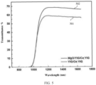
- FIG. 5 shows comparison between transmittance of a magneto-optic thin film including an MgO diffusion barrier layer and transmittance of a magneto-optic thin film not including an MgO diffusion barrier layer.
- a curve 501 indicates the transmittance of the magneto-optic thin film not including an MgO diffusion barrier layer.
- a curve 502 indicates the transmittance of the magneto-optic thin film including the MgO diffusion barrier layer.
- the transmittance of the magneto-optic thin film including the MgO diffusion barrier layer is greater than the transmittance of the magneto-optic thin film not including an MgO diffusion barrier layer. Therefore, the magneto-optic thin film including the MgO diffusion barrier layer can provide higher optical performance.
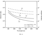
- FIG. 6 shows comparison between a refractive index of a magneto-optic thin film including an MgO diffusion barrier layer and a refractive index of a magneto-optic thin film not including an MgO diffusion barrier layer, and comparison between an extinction coefficient of the magneto-optic thin film including the MgO diffusion barrier layer and an extinction coefficient of the magneto-optic thin film not including an MgO diffusion barrier layer.
- a curve 601 indicates the refractive index of the magneto-optic thin film not including an MgO diffusion barrier layer.
- a curve 602 indicates the refractive index of the magneto-optic thin film including the MgO diffusion barrier layer.
- a curve 603 indicates the extinction coefficient of the magneto-optic thin film not including an MgO diffusion barrier layer.
- a curve 604 indicates the extinction coefficient of the magneto-optic thin film including the MgO diffusion barrier layer. As shown in FIG. 6 , compared with the magneto-optic thin film not including an MgO diffusion barrier layer, the magneto-optic thin film including the MgO diffusion barrier layer has a smaller refractive index and extinction coefficient.
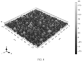
- FIG. 7 shows surface morphology of YIG grains captured by an atomic force microscope.
- FIG. 8 shows surface morphology of Ce:YIG captured by an atomic force microscope.
- YIG grains are small, nucleation sites are uniform, and most of the nucleation sites face upward. This facilitates preferred orientation of Ce:YIG and achieves good crystallinity.
Landscapes
- Physics & Mathematics (AREA)
- Chemical & Material Sciences (AREA)
- Nonlinear Science (AREA)
- Engineering & Computer Science (AREA)
- General Physics & Mathematics (AREA)
- Optics & Photonics (AREA)
- Organic Chemistry (AREA)
- Crystallography & Structural Chemistry (AREA)
- Materials Engineering (AREA)
- Metallurgy (AREA)
- Power Engineering (AREA)
- Inorganic Chemistry (AREA)
- Chemical Kinetics & Catalysis (AREA)
- General Chemical & Material Sciences (AREA)
- Optical Modulation, Optical Deflection, Nonlinear Optics, Optical Demodulation, Optical Logic Elements (AREA)
- Thin Magnetic Films (AREA)
Applications Claiming Priority (2)
| Application Number | Priority Date | Filing Date | Title |
|---|---|---|---|
| CN202111040113.0A CN113741068B (zh) | 2021-09-06 | 2021-09-06 | 磁光薄膜、光隔离器以及制造磁光薄膜的方法 |
| PCT/CN2022/116269 WO2023030397A1 (zh) | 2021-09-06 | 2022-08-31 | 磁光薄膜、光隔离器以及制造磁光薄膜的方法 |
Publications (2)
| Publication Number | Publication Date |
|---|---|
| EP4386473A1 true EP4386473A1 (de) | 2024-06-19 |
| EP4386473A4 EP4386473A4 (de) | 2024-12-18 |
Family
ID=78736177
Family Applications (1)
| Application Number | Title | Priority Date | Filing Date |
|---|---|---|---|
| EP22863532.2A Pending EP4386473A4 (de) | 2021-09-06 | 2022-08-31 | Magnetooptischer dünnfilm, optischer isolator und verfahren zur herstellung eines magnetooptischen dünnfilms |
Country Status (4)
| Country | Link |
|---|---|
| US (1) | US20240248333A1 (de) |
| EP (1) | EP4386473A4 (de) |
| CN (1) | CN113741068B (de) |
| WO (1) | WO2023030397A1 (de) |
Families Citing this family (2)
| Publication number | Priority date | Publication date | Assignee | Title |
|---|---|---|---|---|
| CN113741068B (zh) * | 2021-09-06 | 2024-06-18 | 华为技术有限公司 | 磁光薄膜、光隔离器以及制造磁光薄膜的方法 |
| CN118112828A (zh) * | 2024-04-30 | 2024-05-31 | 上海铭锟半导体有限公司 | 一种磁光效应驱动的非易失性光开关及其制备方法 |
Family Cites Families (8)
| Publication number | Priority date | Publication date | Assignee | Title |
|---|---|---|---|---|
| JP2889463B2 (ja) * | 1992-11-05 | 1999-05-10 | 富士ゼロックス株式会社 | 配向性強誘電体薄膜素子 |
| CN103255384B (zh) * | 2013-05-15 | 2016-08-10 | 电子科技大学 | 晶粒c轴垂直膜面取向生长的钡铁氧体薄膜制备方法 |
| CN105714379B (zh) * | 2016-02-26 | 2018-07-27 | 电子科技大学 | 一种硅上直接生长高掺杂钇铁石榴石薄膜的制备方法 |
| CN109440071B (zh) * | 2018-12-26 | 2020-12-29 | 电子科技大学 | 一种硅集成低光学损耗磁光薄膜及其制备方法 |
| US12560832B2 (en) * | 2019-04-23 | 2026-02-24 | Regents Of The University Of Minnesota | High gyrotropy photonic isolators directly on substrate |
| TWI764399B (zh) * | 2020-04-27 | 2022-05-11 | 台灣積體電路製造股份有限公司 | 半導體裝置、積體晶片及其形成方法 |
| WO2022051750A1 (en) * | 2020-09-03 | 2022-03-10 | Vida Products | Single crystal yig nanofilm fabricated by a metal organic deposition epitaxial growth process |
| CN113741068B (zh) * | 2021-09-06 | 2024-06-18 | 华为技术有限公司 | 磁光薄膜、光隔离器以及制造磁光薄膜的方法 |
-
2021
- 2021-09-06 CN CN202111040113.0A patent/CN113741068B/zh active Active
-
2022
- 2022-08-31 WO PCT/CN2022/116269 patent/WO2023030397A1/zh not_active Ceased
- 2022-08-31 EP EP22863532.2A patent/EP4386473A4/de active Pending
-
2024
- 2024-03-01 US US18/593,284 patent/US20240248333A1/en active Pending
Also Published As
| Publication number | Publication date |
|---|---|
| WO2023030397A1 (zh) | 2023-03-09 |
| EP4386473A4 (de) | 2024-12-18 |
| US20240248333A1 (en) | 2024-07-25 |
| CN113741068B (zh) | 2024-06-18 |
| CN113741068A (zh) | 2021-12-03 |
Similar Documents
| Publication | Publication Date | Title |
|---|---|---|
| US20240248333A1 (en) | Magneto-Optic Thin Film, Optical Isolator, and Method for Manufacturing Magneto-Optic Thin Film | |
| JP3813740B2 (ja) | 電子デバイス用基板 | |
| US6683012B2 (en) | Method for epitaxially growing crystalline insulation layer on crystalline silicon substrate while simultaneously growing silicon oxide, nitride, or oxynitride | |
| Heideman et al. | High quality ZnO layers with adjustable refractive indices for integrated optics applications | |
| US12560832B2 (en) | High gyrotropy photonic isolators directly on substrate | |
| JP2004095843A (ja) | 電子デバイス用基板および電子デバイス | |
| JPH0769523B2 (ja) | 磁気光学アイソレータ装置 | |
| Wolfe et al. | Thin‐film garnet materials with zero linear birefringence for magneto‐optic waveguide devices | |
| CN1314506A (zh) | 磁性石榴石单晶膜及其制法,和使用该单晶膜的法拉第转子 | |
| Pons-Y-Moll et al. | Structural and optical properties of rare-earth-doped Y 2 O 3 waveguides grown by pulsed-laser deposition | |
| CN104988470B (zh) | 一步脉冲激光沉积多层磁光薄膜的方法 | |
| US4959136A (en) | Method for making an amorphous aluminum-nitrogen alloy layer | |
| US4719154A (en) | Magneto-optic recording element with amorphous aluminum-nitrogen alloy layer | |
| US4946241A (en) | Method of manufacturing iron garnet layers | |
| CN109440071B (zh) | 一种硅集成低光学损耗磁光薄膜及其制备方法 | |
| US6641751B1 (en) | Magnetic garnet single crystal and faraday rotator using the same | |
| US5501913A (en) | Garnet polycrystalline film for magneto-optical recording medium | |
| TW202141567A (zh) | 複合基板及其製造方法 | |
| CN111257995A (zh) | 一种高折射率差yag单晶异质结构薄膜波导及其制备方法 | |
| CN111856791A (zh) | 基于模式滤波器的硅基磁光隔离器及制备方法 | |
| CN110172734B (zh) | 一种立方相掺杂铁酸铈磁光材料及其制备方法和应用 | |
| JP3773899B2 (ja) | 磁性半導体材料及びその製造方法 | |
| US5965287A (en) | Magneto-optical element material and Faraday element using the same | |
| CN100399111C (zh) | 法拉第转子及用其的光部件 | |
| CN113564709A (zh) | 一种金属杂质原子掺杂的硅酸铒及其制备方法和应用 |
Legal Events
| Date | Code | Title | Description |
|---|---|---|---|
| STAA | Information on the status of an ep patent application or granted ep patent |
Free format text: STATUS: THE INTERNATIONAL PUBLICATION HAS BEEN MADE |
|
| PUAI | Public reference made under article 153(3) epc to a published international application that has entered the european phase |
Free format text: ORIGINAL CODE: 0009012 |
|
| STAA | Information on the status of an ep patent application or granted ep patent |
Free format text: STATUS: REQUEST FOR EXAMINATION WAS MADE |
|
| 17P | Request for examination filed |
Effective date: 20240313 |
|
| AK | Designated contracting states |
Kind code of ref document: A1 Designated state(s): AL AT BE BG CH CY CZ DE DK EE ES FI FR GB GR HR HU IE IS IT LI LT LU LV MC MK MT NL NO PL PT RO RS SE SI SK SM TR |
|
| DAV | Request for validation of the european patent (deleted) | ||
| DAX | Request for extension of the european patent (deleted) | ||
| A4 | Supplementary search report drawn up and despatched |
Effective date: 20241118 |
|
| RIC1 | Information provided on ipc code assigned before grant |
Ipc: C30B 29/28 20060101ALI20241112BHEP Ipc: C30B 25/18 20060101ALI20241112BHEP Ipc: G02F 1/00 20060101ALI20241112BHEP Ipc: G02F 1/09 20060101AFI20241112BHEP |