EP4381502B1 - Eingangsschaltung für analogen neuronalen speicher in einem künstlichen neuronalen tiefenlernnetz - Google Patents
Eingangsschaltung für analogen neuronalen speicher in einem künstlichen neuronalen tiefenlernnetz Download PDFInfo
- Publication number
- EP4381502B1 EP4381502B1 EP21823704.8A EP21823704A EP4381502B1 EP 4381502 B1 EP4381502 B1 EP 4381502B1 EP 21823704 A EP21823704 A EP 21823704A EP 4381502 B1 EP4381502 B1 EP 4381502B1
- Authority
- EP
- European Patent Office
- Prior art keywords
- row
- input
- array
- digital
- output
- Prior art date
- Legal status (The legal status is an assumption and is not a legal conclusion. Google has not performed a legal analysis and makes no representation as to the accuracy of the status listed.)
- Active
Links
Images




















Classifications
-
- G—PHYSICS
- G11—INFORMATION STORAGE
- G11C—STATIC STORES
- G11C11/00—Digital stores characterised by the use of particular electric or magnetic storage elements; Storage elements therefor
- G11C11/54—Digital stores characterised by the use of particular electric or magnetic storage elements; Storage elements therefor using elements simulating biological cells, e.g. neuron
-
- G—PHYSICS
- G06—COMPUTING OR CALCULATING; COUNTING
- G06F—ELECTRIC DIGITAL DATA PROCESSING
- G06F17/00—Digital computing or data processing equipment or methods, specially adapted for specific functions
- G06F17/10—Complex mathematical operations
- G06F17/16—Matrix or vector computation, e.g. matrix-matrix or matrix-vector multiplication, matrix factorization
-
- G—PHYSICS
- G06—COMPUTING OR CALCULATING; COUNTING
- G06N—COMPUTING ARRANGEMENTS BASED ON SPECIFIC COMPUTATIONAL MODELS
- G06N3/00—Computing arrangements based on biological models
- G06N3/02—Neural networks
- G06N3/04—Architecture, e.g. interconnection topology
- G06N3/044—Recurrent networks, e.g. Hopfield networks
- G06N3/0442—Recurrent networks, e.g. Hopfield networks characterised by memory or gating, e.g. long short-term memory [LSTM] or gated recurrent units [GRU]
-
- G—PHYSICS
- G06—COMPUTING OR CALCULATING; COUNTING
- G06N—COMPUTING ARRANGEMENTS BASED ON SPECIFIC COMPUTATIONAL MODELS
- G06N3/00—Computing arrangements based on biological models
- G06N3/02—Neural networks
- G06N3/06—Physical realisation, i.e. hardware implementation of neural networks, neurons or parts of neurons
- G06N3/063—Physical realisation, i.e. hardware implementation of neural networks, neurons or parts of neurons using electronic means
- G06N3/065—Analogue means
-
- G—PHYSICS
- G11—INFORMATION STORAGE
- G11C—STATIC STORES
- G11C11/00—Digital stores characterised by the use of particular electric or magnetic storage elements; Storage elements therefor
- G11C11/56—Digital stores characterised by the use of particular electric or magnetic storage elements; Storage elements therefor using storage elements with more than two stable states represented by steps, e.g. of voltage, current, phase, frequency
- G11C11/5621—Digital stores characterised by the use of particular electric or magnetic storage elements; Storage elements therefor using storage elements with more than two stable states represented by steps, e.g. of voltage, current, phase, frequency using charge storage in a floating gate
- G11C11/5628—Programming or writing circuits; Data input circuits
-
- G—PHYSICS
- G11—INFORMATION STORAGE
- G11C—STATIC STORES
- G11C27/00—Electric analogue stores, e.g. for storing instantaneous values
- G11C27/02—Sample-and-hold arrangements
- G11C27/024—Sample-and-hold arrangements using a capacitive memory element
-
- G—PHYSICS
- G11—INFORMATION STORAGE
- G11C—STATIC STORES
- G11C27/00—Electric analogue stores, e.g. for storing instantaneous values
- G11C27/04—Shift registers
-
- G—PHYSICS
- G11—INFORMATION STORAGE
- G11C—STATIC STORES
- G11C7/00—Arrangements for writing information into, or reading information out from, a digital store
- G11C7/10—Input/output [I/O] data interface arrangements, e.g. I/O data control circuits, I/O data buffers
- G11C7/1006—Data managing, e.g. manipulating data before writing or reading out, data bus switches or control circuits therefor
-
- H—ELECTRICITY
- H03—ELECTRONIC CIRCUITRY
- H03M—CODING; DECODING; CODE CONVERSION IN GENERAL
- H03M1/00—Analogue/digital conversion; Digital/analogue conversion
- H03M1/12—Analogue/digital converters
- H03M1/34—Analogue value compared with reference values
- H03M1/38—Analogue value compared with reference values sequentially only, e.g. successive approximation type
- H03M1/46—Analogue value compared with reference values sequentially only, e.g. successive approximation type with digital/analogue converter for supplying reference values to converter
- H03M1/462—Details of the control circuitry, e.g. of the successive approximation register
-
- G—PHYSICS
- G06—COMPUTING OR CALCULATING; COUNTING
- G06N—COMPUTING ARRANGEMENTS BASED ON SPECIFIC COMPUTATIONAL MODELS
- G06N3/00—Computing arrangements based on biological models
- G06N3/02—Neural networks
- G06N3/04—Architecture, e.g. interconnection topology
- G06N3/048—Activation functions
-
- G—PHYSICS
- G11—INFORMATION STORAGE
- G11C—STATIC STORES
- G11C27/00—Electric analogue stores, e.g. for storing instantaneous values
- G11C27/02—Sample-and-hold arrangements
- G11C27/024—Sample-and-hold arrangements using a capacitive memory element
- G11C27/028—Current mode circuits, e.g. switched current memories
Definitions
- Numerous embodiments of input circuitry for an analog neural memory in a deep learning artificial neural network are disclosed.
- Artificial neural networks mimic biological neural networks (the central nervous systems of animals, in particular the brain) and are used to estimate or approximate functions that can depend on a large number of inputs and are generally unknown. Artificial neural networks generally include layers of interconnected "neurons" which exchange messages between each other.
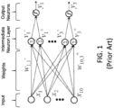
- Figure 1 illustrates an artificial neural network, where the circles represent the inputs or layers of neurons.
- the connections (called synapses) are represented by arrows and have numeric weights that can be tuned based on experience.
- neural networks include a layer of multiple inputs.
- the neurons at each level individually or collectively make a decision based on the received data from the synapses.
- the non-volatile memory arrays operate as an analog neural memory.
- the neural network device includes a first plurality of synapses configured to receive a first plurality of inputs and to generate therefrom a first plurality of outputs, and a first plurality of neurons configured to receive the first plurality of outputs.
- the first plurality of synapses includes a plurality of memory cells, wherein each of the memory cells includes spaced apart source and drain regions formed in a semiconductor substrate with a channel region extending there between, a floating gate disposed over and insulated from a first portion of the channel region and a non-floating gate disposed over and insulated from a second portion of the channel region.
- Each of the plurality of memory cells is configured to store a weight value corresponding to a number of electrons on the floating gate.
- the plurality of memory cells is configured to multiply the first plurality of inputs by the stored weight values to generate the first plurality of outputs.
- Non-volatile memories are well known.
- U.S. Patent 5,029,130 (“the '130 patent”) discloses an array of split gate non-volatile memory cells, which are a type of flash memory cells.
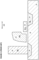
- Such a memory cell 210 is shown in Figure 2 .
- Each memory cell 210 includes source region 14 and drain region 16 formed in semiconductor substrate 12, with channel region 18 there between.
- Floating gate 20 is formed over and insulated from (and controls the conductivity of) a first portion of the channel region 18, and over a portion of the source region 14.
- Word line terminal 22 (which is typically coupled to a word line) has a first portion that is disposed over and insulated from (and controls the conductivity of) a second portion of the channel region 18, and a second portion that extends up and over the floating gate 20.
- the floating gate 20 and word line terminal 22 are insulated from the substrate 12 by a gate oxide.
- Bitline 24 is coupled to drain region 16.
- Memory cell 210 is erased (where electrons are removed from the floating gate) by placing a high positive voltage on the word line terminal 22, which causes electrons on the floating gate 20 to tunnel through the intermediate insulation from the floating gate 20 to the word line terminal 22 via Fowler-Nordheim (FN) tunneling.
- FN Fowler-Nordheim
- Memory cell 210 is programmed by source side injection (SSI) with hot electrons (where electrons are placed on the floating gate) by placing a positive voltage on the word line terminal 22, and a positive voltage on the source region 14. Electron current will flow from the drain region 16 towards the source region 14. The electrons will accelerate and become heated when they reach the gap between the word line terminal 22 and the floating gate 20. Some of the heated electrons will be injected through the gate oxide onto the floating gate 20 due to the attractive electrostatic force from the floating gate 20.
- SSI source side injection
- Memory cell 210 is read by placing positive read voltages on the drain region 16 and word line terminal 22 (which turns on the portion of the channel region 18 under the word line terminal). If the floating gate 20 is positively charged (i.e., erased of electrons), then the portion of the channel region 18 under the floating gate 20 is turned on as well, and current will flow across the channel region 18, which is sensed as the erased or "1" state. If the floating gate 20 is negatively charged (i.e., programmed with electrons), then the portion of the channel region under the floating gate 20 is mostly or entirely turned off, and current will not flow (or there will be little flow) across the channel region 18, which is sensed as the programmed or "0" state.
- Table No. 1 depicts typical voltage and current ranges that can be applied to the terminals of memory cell 110 for performing read, erase, and program operations: Table No. 1: Operation of Flash Memory Cell 210 of Figure 3 WL BL SL Read 2-3V 0.6-2V 0V Erase ⁇ 11-13V 0V 0V Program 1-2V 10.5-3 ⁇ A 9-10V
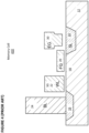
- Figure 3 depicts a four-gate memory cell 310 comprising source region 14, drain region 16, floating gate 20 over a first portion of channel region 18, a select gate 22 (typically coupled to a word line, WL) over a second portion of the channel region 18, a control gate 28 over the floating gate 20, and an erase gate 30 over the source region 14.
- WL word line
- FIG. 3 depicts a four-gate memory cell 310 comprising source region 14, drain region 16, floating gate 20 over a first portion of channel region 18, a select gate 22 (typically coupled to a word line, WL) over a second portion of the channel region 18, a control gate 28 over the floating gate 20, and an erase gate 30 over the source region 14.
- WL word line
- erase gate 30 over the source region 14.
- All gates are non-floating gates except floating gate 20, meaning that they are electrically connected or connectable to a voltage source. Programming is performed by heated electrons from the channel region 18 injecting themselves onto the floating gate 20. Erasing is performed by electrons tunneling from the floating gate
- Table No. 2 depicts typical voltage and current ranges that can be applied to the terminals of memory cell 310 for performing read, erase, and program operations: Table No. 2: Operation of Flash Memory Cell 310 of Figure 3 WL/SG BL CG EG SL Read 1.0-2V 0.6-2V 0-2.6V 0-2.6V 0V Erase -0.5V/0V 0V 0V/-8V 8-12V 0V Program 1V 0.1-1 ⁇ A 8-11V 4.5-9V 4.5-5V
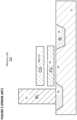
- Figure 4 depicts a three-gate memory cell 410, which is another type of flash memory cell.
- Memory cell 410 is identical to the memory cell 310 of Figure 3 except that memory cell 410 does not have a separate control gate.
- the erase operation (whereby erasing occurs through use of the erase gate) and read operation are similar to that of the Figure 3 except there is no control gate bias applied.
- the programming operation also is done without the control gate bias, and as a result, a higher voltage must be applied on the source line during a program operation to compensate for a lack of control gate bias.
- Table No. 3 depicts typical voltage and current ranges that can be applied to the terminals of memory cell 410 for performing read, erase, and program operations: Table No. 3: Operation of Flash Memory Cell 410 of Figure 4 WL/SG BL EG SL Read 0.7-2.2V 0.6-2V 0-2.6V 0V Erase -0.5V/0V 0V 11.5V 0V Program 1V 0.2-3 ⁇ A 4.5V 7-9V
- Figure 5 depicts stacked gate memory cell 510, which is another type of flash memory cell.
- Memory cell 510 is similar to memory cell 210 of Figure 2 , except that floating gate 20 extends over the entire channel region 18, and control gate 22 (which here will be coupled to a word line) extends over floating gate 20, separated by an insulating layer (not shown).
- the erase is done by FN tunneling of electrons from FG to substrate, programming is by channel hot electron (CHE) injection at region between the channel 18 and the drain region 16, by the electrons flowing from the source region 14 towards to drain region 16 and read operation which is similar to that for memory cell 210 with a higher control gate voltage.
- CHE channel hot electron
- Table No. 4 depicts typical voltage ranges that can be applied to the terminals of memory cell 510 and substrate 12 for performing read, erase, and program operations: Table No. 4: Operation of Flash Memory Cell 510 of Figure 5 CG BL SL Substrate Read 2-5V 0.6 - 2V 0V 0V Erase -8 to -10V/0V FLT FLT 8-10V / 15-20V Program 8-12V 3-5V 0V 0V
- non-volatile memory technologies such as FINFET split gate flash or stack gate flash memory, NAND flash, SONOS (silicon-oxide-nitride-oxide-silicon, charge trap in nitride), MONOS (metal-oxide-nitride-oxide-silicon, metal charge trap in nitride), ReRAM (resistive ram), PCM (phase change memory), MRAM (magnetic ram), FeRAM (ferroelectric ram), CT (charge trap) memory, CN (carbontube) memory, OTP (bi-level or multi-level one time programmable), and CeRAM (correlated electron ram), without limitation.
- SONOS silicon-oxide-nitride-oxide-silicon, charge trap in nitride
- MONOS metal-oxide-nitride-oxide-silicon, metal charge trap in nitride
- ReRAM resistive ram
- PCM phase change memory
- MRAM magnetic ram
- FeRAM ferrr
- the lines are configured so that each memory cell can be individually programmed, erased, and read without adversely affecting the memory state of other memory cells in the array, as further explained below.
- continuous (analog) programming of the memory cells is provided.
- the memory state (i.e., charge on the floating gate) of each memory cell in the array can be continuously changed from a fully erased state to a fully programmed state, independently and with minimal disturbance of other memory cells.
- the memory state (i.e., charge on the floating gate) of each memory cell in the array can be continuously changed from a fully programmed state to a fully erased state, and vice-versa, independently and with minimal disturbance of other memory cells.
- the cell storage is analog or at the very least can store one of many discrete values (such as 16 or 64 different values), which allows for very precise and individual tuning of all the cells in the memory array, and which makes the memory array ideal for storing and making fine tuning adjustments to the synapsis weights of the neural network.
- Figure 6 conceptually illustrates a non-limiting example of a neural network utilizing a non-volatile memory array of the present embodiments.
- This example uses the non-volatile memory array neural network for a facial recognition application, but any other appropriate application could be implemented using a non-volatile memory array based neural network.
- S0 is the input layer, which for this example is a 32x32 pixel RGB image with 5 bit precision (i.e. three 32x32 pixel arrays, one for each color R, G and B, each pixel being 5 bit precision).
- the synapses CB1 going from input layer S0 to layer C1 apply different sets of weights in some instances and shared weights in other instances and scan the input image with 3x3 pixel overlapping filters (kernel), shifting the filter by 1 pixel (or more than 1 pixel as dictated by the model).
- values for 9 pixels in a 3x3 portion of the image are provided to the synapses CB1, where these 9 input values are multiplied by the appropriate weights and, after summing the outputs of that multiplication, a single output value is determined and provided by a first synapse of CB1 for generating a pixel of one of the feature maps of layer C1.
- the 3x3 filter is then shifted one pixel to the right within input layer S0 (i.e., adding the column of three pixels on the right, and dropping the column of three pixels on the left), whereby the 9 pixel values in this newly positioned filter are provided to the synapses CB1, where they are multiplied by the same weights and a second single output value is determined by the associated synapse.
- This process is continued until the 3x3 filter scans across the entire 32x32 pixel image of input layer S0, for all three colors and for all bits (precision values).
- the process is then repeated using different sets of weights to generate a different feature map of layer C1, until all the features maps of layer C1 have been calculated.
- layer C1 in the present example, there are 16 feature maps, with 30x30 pixels each. Each pixel is a new feature pixel extracted from multiplying the inputs and kernel, and therefore each feature map is a two dimensional array, and thus in this example layer C1 constitutes 16 layers of two dimensional arrays (keeping in mind that the layers and arrays referenced herein are logical relationships, not necessarily physical relationships - i.e., the arrays are not necessarily oriented in physical two dimensional arrays). Each of the 16 feature maps in layer C1 is generated by one of sixteen different sets of synapse weights applied to the filter scans. The C1 feature maps could all be directed to different aspects of the same image feature, such as boundary identification.
- the first map (generated using a first weight set, shared for all scans used to generate this first map) could identify circular edges
- the second map generated using a second weight set different from the first weight set
- An activation function P1 (pooling) is applied before going from layer C1 to layer S1, which pools values from consecutive, non-overlapping 2x2 regions in each feature map.
- the purpose of the pooling function P1 is to average out the nearby location (or a max function can also be used), to reduce the dependence of the edge location for example and to reduce the data size before going to the next stage.
- layer S1 there are 16 15x15 feature maps (i.e., sixteen different arrays of 15x15 pixels each).
- the synapses CB2 going from layer S1 to layer C2 scan maps in layer S1 with 4x4 filters, with a filter shift of 1 pixel.
- An activation function P2 (pooling) is applied before going from layer C2 to layer S2, which pools values from consecutive non-overlapping 2x2 regions in each feature map.
- layer S2 there are 22 6x6 feature maps.
- An activation function (pooling) is applied at the synapses CB3 going from layer S2 to layer C3, where every neuron in layer C3 connects to every map in layer S2 via a respective synapse of CB3.
- the synapses CB4 going from layer C3 to the output layer S3 fully connects C3 to S3, i.e. every neuron in layer C3 is connected to every neuron in layer S3.
- the output at S3 includes 10 neurons, where the highest output neuron determines the class. This output could, for example, be indicative of an identification or classification of the contents of the original image.
- Each layer of synapses is implemented using an array, or a portion of an array, of non-volatile memory cells.
- FIG. 7 is a block diagram of an array that can be used for that purpose.
- VMM array 32 includes non-volatile memory cells and is utilized as the synapses (such as CB1, CB2, CB3, and CB4 in Figure 6 ) between one layer and the next layer.
- VMM array 32 includes an array of non-volatile memory cells 33, erase gate and word line gate decoder 34, control gate decoder 35, bit line decoder 36 and source line decoder 37, which decode the respective inputs for the non-volatile memory cell array 33.
- Input to VMM array 32 can be from the erase gate and wordline gate decoder 34 or from the control gate decoder 35.
- Source line decoder 37 in this example also decodes the output of the non-volatile memory cell array 33.
- bit line decoder 36 can decode the output of the non-volatile memory cell array 33.
- Non-volatile memory cell array 33 serves two purposes. First, it stores the weights that will be used by the VMM array 32. Second, the non-volatile memory cell array 33 effectively multiplies the inputs by the weights stored in the non-volatile memory cell array 33 and adds them up per output line (source line or bit line) to produce the output, which will be the input to the next layer or input to the final layer. By performing the multiplication and addition function, the non-volatile memory cell array 33 negates the need for separate multiplication and addition logic circuits and is also power efficient due to its in-situ memory computation.
- the output of non-volatile memory cell array 33 is supplied to a differential summer (such as a summing op-amp or a summing current mirror) 38, which sums up the outputs of the non-volatile memory cell array 33 to create a single value for that convolution.
- the differential summer 38 is arranged to perform summation of positive weight and negative weight.
- non-volatile memory cell array 33 constitutes a plurality of synapses (which receive their inputs from the prior layer of neurons or from an input layer such as an image database), and summing op-amp 38 and activation function block 39 constitute a plurality of neurons.
- the input to VMM array 32 in Figure 7 can be analog level, binary level, or digital bits (in which case a DAC is provided to convert digital bits to appropriate input analog level) and the output can be analog level, binary level, or digital bits (in which case an output ADC is provided to convert output analog level into digital bits).
- FIG. 8 is a block diagram depicting the usage of numerous layers of VMM arrays 32, here labeled as VMM arrays 32a, 32b, 32c, 32d, and 32e.
- the input denoted Inputx
- the converted analog inputs could be voltage or current.
- the input D/A conversion for the first layer could be done by using a function or a LUT (look up table) that maps the inputs Inputx to appropriate analog levels for the matrix multiplier of input VMM array 32a.
- the input conversion could also be done by an analog to analog (A/A) converter to convert an external analog input to a mapped analog input to the input VMM array 32a.
- A/A analog to analog
- VMM array 32a The output generated by input VMM array 32a is provided as an input to the next VMM array (hidden level 1) 32b, which in turn generates an output that is provided as an input to the next VMM array (hidden level 2) 32c, and so on.
- the various layers of VMM array 32 function as different layers of synapses and neurons of a convolutional neural network (CNN).
- CNN convolutional neural network
- Each VMM array 32a, 32b, 32c, 32d, and 32e can be a stand-alone, physical non-volatile memory array, or multiple VMM arrays could utilize different portions of the same physical non-volatile memory array, or multiple VMM arrays could utilize overlapping portions of the same physical non-volatile memory array.
- FIG. 8 contains five layers (32a,32b,32c,32d,32e): one input layer (32a), two hidden layers (32b,32c), and two fully connected layers (32d,32e).
- one input layer 32a
- two hidden layers 32b,32c
- two fully connected layers 32d,32e
- VMM Vector-by-Matrix Multiplication
- FIG 9 depicts neuron VMM array 900, which is particularly suited for memory cells 310 as shown in Figure 3 and is utilized as the synapses and parts of neurons between an input layer and the next layer.
- VMM array 900 comprises memory array 901 of non-volatile memory cells and reference array 902 (at the top of the array) of non-volatile reference memory cells. Alternatively, another reference array can be placed at the bottom.
- control gate lines such as control gate line 903, run in a vertical direction (hence reference array 902 in the row direction is orthogonal to control gate line 903)
- erase gate lines such as erase gate line 904, run in a horizontal direction.
- the inputs to VMM array 900 are provided on the control gate lines (CGO, CG1, CG2, CG3), and the output of VMM array 900 emerges on the source lines (SLO, SL1).
- SLO, SL1 source lines
- the current placed on each source line (SLO, SL1, respectively) performs a summing function of all the currents from the memory cells connected to that particular source line.
- the non-volatile memory cells of VMM array 900 i.e., the memory cells 310 of VMM array 900, are preferably configured to operate in a sub-threshold region.
- Vg n * Vt * log Ids / wp * Io
- wp is w of a reference or peripheral memory cell.
- wa w of each memory cell in the memory array.
- Vthp is effective threshold voltage of the peripheral memory cell and Vtha is effective threshold voltage of the main (data) memory cell.
- the threshold voltage of a transistor is a function of substrate body bias voltage and the substrate body bias voltage, denoted Vsb, can be modulated to compensate for various conditions, on such temperature.
- Vth0 is threshold voltage with zero substrate bias
- ⁇ F is a surface potential
- gamma is a body effect parameter
- a wordline or control gate can be used as the input for the memory cell for the input voltage.
- a wordline or control gate or bitline or sourceline can be used as the input for the memory cell operated in the linear region.
- the bitline or sourceline can be used as the output for the memory cell.
- a memory cell such as a reference memory cell or a peripheral memory cell
- a transistor operating in the linear region can be used to linearly convert an input/output current into an input/output voltage.
- a wordline, control gate, or erase gate can be used as the input for the memory cell operated in the saturation region.
- the bitline or sourceline can be used as the output for the output neuron.
- the memory cells of VMM arrays described herein can be used in all regions or a combination thereof (sub threshold, linear, or saturation) for each layer or multi layers of a neural network.
- VMM array 32 of Figure 7 Other embodiments for VMM array 32 of Figure 7 are described in U.S. Patent No. 10,748,630 . As described in that application. a sourceline or a bitline can be used as the neuron output (current summation output).
- FIG 10 depicts neuron VMM array 1000, which is particularly suited for memory cells 210 as shown in Figure 2 and is utilized as the synapses between an input layer and the next layer.
- VMM array 1000 comprises a memory array 1003 of non-volatile memory cells, reference array 1001 of first non-volatile reference memory cells, and reference array 1002 of second non-volatile reference memory cells.
- Reference arrays 1001 and 1002, arranged in the column direction of the array, serve to convert current inputs flowing into terminals BLR0, BLR1, BLR2, and BLR3 into voltage inputs WL0, WL1, WL2, and WL3.
- the first and second non-volatile reference memory cells are diode-connected through multiplexors 1014 (only partially depicted) with current inputs flowing into them.
- the reference cells are tuned (e.g., programmed) to target reference levels.
- the target reference levels are provided by a reference mini-array matrix (not shown).
- Memory array 1003 serves two purposes. First, it stores the weights that will be used by the VMM array 1000 on respective memory cells thereof. Second, memory array 1003 effectively multiplies the inputs (i.e. current inputs provided in terminals BLR0, BLR1, BLR2, and BLR3, which reference arrays 1001 and 1002 convert into the input voltages to supply to wordlines WL0, WL1, WL2, and WL3) by the weights stored in the memory array 1003 and then adds all the results (memory cell currents) to produce the output on the respective bit lines (BL0 - BLN), which will be the input to the next layer or input to the final layer.
- inputs i.e. current inputs provided in terminals BLR0, BLR1, BLR2, and BLR3, which reference arrays 1001 and 1002 convert into the input voltages to supply to wordlines WL0, WL1, WL2, and WL3
- memory array 1003 negates the need for separate multiplication and addition logic circuits and is also power efficient.
- the voltage inputs are provided on the word lines WL0, WL1, WL2, and WL3, and the output emerges on the respective bit lines BL0 - BLN during a read (inference) operation.
- the current placed on each of the bit lines BL0 - BLN performs a summing function of the currents from all non-volatile memory cells connected to that particular bitline.
- Table No. 5 depicts operating voltages and currents for VMM array 1000.
- the columns in the table indicate the voltages placed on word lines for selected cells, word lines for unselected cells, bit lines for selected cells, bit lines for unselected cells, source lines for selected cells, and source lines for unselected cells.
- the rows indicate the operations of read, erase, and program.
- VMM Array 1000 of Figure 10 Operation of VMM Array 1000 of Figure 10: WL WL -unsel BL BL -unsel SL SL -unsel Read 1-3.5V -0.5V/0V 0.6-2V (Ineuron) 0.6V-2V/0V 0V 0V Erase ⁇ 5-13V 0V 0V 0V 0V 0V Program 1-2V -0.5V/0V 0.1-3 uA Vinh ⁇ 2.5V 4-10V 0-1V/FLT
- FIG 11 depicts neuron VMM array 1100, which is particularly suited for memory cells 210 as shown in Figure 2 and is utilized as the synapses and parts of neurons between an input layer and the next layer.
- VMM array 1100 comprises a memory array 1103 of non-volatile memory cells, reference array 1101 of first non-volatile reference memory cells, and reference array 1102 of second non-volatile reference memory cells. Reference arrays 1101 and 1102 run in row direction of the VMM array 1100.
- VMM array is similar to VMM 1000 except that in VMM array 1100, the word lines run in the vertical direction.
- the inputs are provided on the word lines (WLA0, WLB0, WLA1, WLB2, WLA2, WLB2, WLA3, WLB3), and the output emerges on the source line (SL0, SL1) during a read operation.
- the current placed on each source line performs a summing function of all the currents from the memory cells connected to that particular source line.
- Table No. 6 depicts operating voltages and currents for VMM array 1100.
- the columns in the table indicate the voltages placed on word lines for selected cells, word lines for unselected cells, bit lines for selected cells, bit lines for unselected cells, source lines for selected cells, and source lines for unselected cells.
- the rows indicate the operations of read, erase, and program.
- VMM Array 1100 of Figure 11 WL WL -unsel BL BL -unsel SL SL -unsel Read 1-3.5V -0.5V/0V 0.6-2V 0.6V-2V/0V ⁇ 0.3-1V (Ineuron) 0V Erase ⁇ 5-13V 0V 0V 0V 0V SL-inhibit ( ⁇ 4-8V) Program 1-2V -0.5V/0V 0.1-3 uA Vinh ⁇ 2.5V 4-10V 0-1V/FLT
- FIG. 12 depicts neuron VMM array 1200, which is particularly suited for memory cells 310 as shown in Figure 3 and is utilized as the synapses and parts of neurons between an input layer and the next layer.
- VMM array 1200 comprises a memory array 1203 of non-volatile memory cells, reference array 1201 of first non-volatile reference memory cells, and reference array 1202 of second non-volatile reference memory cells.
- Reference arrays 1201 and 1202 serve to convert current inputs flowing into terminals BLR0, BLR1, BLR2, and BLR3 into voltage inputs CG0, CG1, CG2, and CG3.
- the first and second non-volatile reference memory cells are diode-connected through multiplexors 1212 (only partially shown) with current inputs flowing into them through BLR0, BLR1, BLR2, and BLR3.
- Multiplexors 1212 each include a respective multiplexor 1205 and a cascoding transistor 1204 to ensure a constant voltage on the bitline (such as BLR0) of each of the first and second non-volatile reference memory cells during a read operation.
- the reference cells are tuned to target reference levels.
- Memory array 1203 serves two purposes. First, it stores the weights that will be used by the VMM array 1200. Second, memory array 1203 effectively multiplies the inputs (current inputs provided to terminals BLR0, BLR1, BLR2, and BLR3, for which reference arrays 1201 and 1202 convert these current inputs into the input voltages to supply to the control gates (CGO, CG1, CG2, and CG3) by the weights stored in the memory array and then add all the results (cell currents) to produce the output, which appears on BL0 - BLN, and will be the input to the next layer or input to the final layer. By performing the multiplication and addition function, the memory array negates the need for separate multiplication and addition logic circuits and is also power efficient.
- the inputs are provided on the control gate lines (CGO, CG1, CG2, and CG3), and the output emerges on the bitlines (BL0 - BLN) during a read operation.
- the current placed on each bitline performs a summing function of all the currents from the memory cells connected to that particular bitline.
- VMM array 1200 implements uni-directional tuning for non-volatile memory cells in memory array 1203. That is, each non-volatile memory cell is erased and then partially programmed until the desired charge on the floating gate is reached. If too much charge is placed on the floating gate (such that the wrong value is stored in the cell), the cell is erased and the sequence of partial programming operations starts over. As shown, two rows sharing the same erase gate (such as EG0 or EG1) are erased together (which is known as a page erase), and thereafter, each cell is partially programmed until the desired charge on the floating gate is reached.
- EG0 or EG1 two rows sharing the same erase gate
- Table No. 7 depicts operating voltages and currents for VMM array 1200.
- the columns in the table indicate the voltages placed on word lines for selected cells, word lines for unselected cells, bit lines for selected cells, bit lines for unselected cells, control gates for selected cells, control gates for unselected cells in the same sector as the selected cells, control gates for unselected cells in a different sector than the selected cells, erase gates for selected cells, erase gates for unselected cells, source lines for selected cells, and source lines for unselected cells.
- the rows indicate the operations of read, erase, and program.
- VMM Array 1200 of Figure 12 WL WL - unsel BL - unsel CG CG- unsel same sector CG- unsel EG EG - unsel SL SL - unsel Read 1.0-2V -0.5V/ 0V 0.6-2V (Ineuron) 0V 0-2.6V 0-2.6V 0-2.6V 0-2.6V 0V 0V Erase 0V 0V 0V 0V 0V 0V 0-2.6V 0-2.6V 5-12V 0-2.6V 0V 0V Program 0.7-1V -0.5V/ 0V 0.1-1uA Vinh (1-2V) 4-11V 0-2.6V 0-2.6V 4.5-5V 0-2.6V 4.5-5V 0-1V
- FIG. 13 depicts neuron VMM array 1300, which is particularly suited for memory cells 310 as shown in Figure 3 , and is utilized as the synapses and parts of neurons between an input layer and the next layer.
- VMM array 1300 comprises a memory array 1303 of non-volatile memory cells, reference array 1301 or first non-volatile reference memory cells, and reference array 1302 of second non-volatile reference memory cells.
- EG lines EGR0, EG0, EG1 and EGR1 are run vertically while CG lines CG0, CG1, CG2 and CG3 and SL lines WL0, WL1, WL2 and WL3 are run horizontally.
- VMM array 1300 is similar to VMM array 1400, except that VMM array 1300 implements bi-directional tuning, where each individual cell can be completely erased, partially programmed, and partially erased as needed to reach the desired amount of charge on the floating gate due to the use of separate EG lines.
- reference arrays 1301 and 1302 convert input current in the terminal BLR0, BLR1, BLR2, and BLR3 into control gate voltages CG0, CG1, CG2, and CG3 (through the action of diode-connected reference cells through multiplexors 1314) to be applied to the memory cells in the row direction.
- the current output (neuron) is in the bitlines BL0 - BLN, where each bit line sums all currents from the non-volatile memory cells connected to that particular bitline.
- Table No. 8 depicts operating voltages and currents for VMM array 1300.
- the columns in the table indicate the voltages placed on word lines for selected cells, word lines for unselected cells, bit lines for selected cells, bit lines for unselected cells, control gates for selected cells, control gates for unselected cells in the same sector as the selected cells, control gates for unselected cells in a different sector than the selected cells, erase gates for selected cells, erase gates for unselected cells, source lines for selected cells, and source lines for unselected cells.
- the rows indicate the operations of read, erase, and program.
- VMM Array 1300 of Figure 13 WL WL - unsel BL BL - unsel CG CG -unsel same sector CG- unsel EG EG- unsel SL SL - unsel Read 1.0-2V -0.5V/ 0V 0.6-2V (Ineuron) 0V 0-2.6V 0-2.6V 0-2.6V 0-2.6V 0V 0V Erase 0V 0V 0V 0V 0V 0V 4-9V 0-2.6V 5-12V 0-2.6V 0V 0V Program 0.7-1V -0.5V/ 0V 0.1-1uA Vinh (1-2V) 4-11V 0-2.6V 0-2.6V 4.5-5V 0-2.6V 4.5-5V 0-1V
- Figure 22 depicts neuron VMM array 2200, which is particularly suited for memory cells 210 as shown in Figure 2 and is utilized as the synapses and parts of neurons between an input layer and the next layer.
- VMM array 2200 the inputs INPUT 0 ...., INPUT N are received on bit lines BL 0 , . . . BL N , respectively, and the outputs OUTPUT 1 , OUTPUT 2 , OUTPUT 3 , and OUTPUT 4 are generated on source lines SL 0 , SL 1 , SL 2 , and SL 3 , respectively.
- Figure 23 depicts neuron VMM array 2300, which is particularly suited for memory cells 210 as shown in Figure 2 and is utilized as the synapses and parts of neurons between an input layer and the next layer.
- the inputs INPUT 0 , INPUT 1 , INPUT 2 , and INPUT 3 are received on source lines SL 0 , SL 1 , SL 2 , and SL 3 , respectively, and the outputs OUTPUT 0 , . . . OUTPUT N are generated on bit lines BL 0 , ..., BL N .
- Figure 24 depicts neuron VMM array 2400, which is particularly suited for memory cells 210 as shown in Figure 2 , and is utilized as the synapses and parts of neurons between an input layer and the next layer.
- the inputs INPUT 0 , ..., INPUT M are received on word lines WL 0 , ..., WL M , respectively, and the outputs OUTPUT 0 , . . . OUTPUT N are generated on bit lines BL 0 , ..., BL N .
- Figure 25 depicts neuron VMM array 2500, which is particularly suited for memory cells 310 as shown in Figure 3 , and is utilized as the synapses and parts of neurons between an input layer and the next layer.
- the inputs INPUT 0 , ..., INPUT M are received on word lines WL 0 , ..., WL M , respectively, and the outputs OUTPUT 0 , . . . OUTPUT N are generated on bit lines BL 0 , ..., BL N .
- Figure 26 depicts neuron VMM array 2600, which is particularly suited for memory cells 410 as shown in Figure 4 , and is utilized as the synapses and parts of neurons between an input layer and the next layer.
- the inputs INPUT 0 , ..., INPUT n are received on vertical control gate lines CG 0 , ..., CG N , respectively, and the outputs OUTPUT 1 and OUTPUT 2 are generated on source lines SL 0 and SL 1 .
- Figure 27 depicts neuron VMM array 2700, which is particularly suited for memory cells 410 as shown in Figure 4 , and is utilized as the synapses and parts of neurons between an input layer and the next layer.
- the inputs INPUT 0 , ..., INPUT N are received on the gates of bit line control gates 2701-1, 2701-2, ..., 2701-(N-1), and 2701-N, respectively, which are coupled to bit lines BL 0 , ..., BL N , respectively.
- Exemplary outputs OUTPUT 1 and OUTPUT 2 are generated on source lines SL 0 and SL 1 .
- Figure 28 depicts neuron VMM array 2800, which is particularly suited for memory cells 310 as shown in Figure 3 , memory cells 510 as shown in Figure 5 , and memory cells 710 as shown in Figure 7 , and is utilized as the synapses and parts of neurons between an input layer and the next layer.
- the inputs INPUT 0 , ..., INPUT M are received on word lines WL 0 , ..., WL M
- the outputs OUTPUT 0 , ..., OUTPUT N are generated on bit lines BL 0 , ..., BL N , respectively.
- Figure 29 depicts neuron VMM array 2900, which is particularly suited for memory cells 310 as shown in Figure 3 , memory cells 510 as shown in Figure 5 , and memory cells 710 as shown in Figure 7 , and is utilized as the synapses and parts of neurons between an input layer and the next layer.
- the inputs INPUT 0 , ..., INPUT M are received on control gate lines CG 0 , ..., CG M .
- Outputs OUTPUT 0 , ..., OUTPUT N are generated on vertical source lines SL 0 , ..., SL N , respectively, where each source line SL i is coupled to the source lines of all memory cells in column i.
- Figure 30 depicts neuron VMM array 3000, which is particularly suited for memory cells 310 as shown in Figure 3 , memory cells 510 as shown in Figure 5 , and memory cells 710 as shown in Figure 7 , and is utilized as the synapses and parts of neurons between an input layer and the next layer.
- the inputs INPUT 0 , ..., INPUT M are received on control gate lines CG 0 , ..., CG M .
- Outputs OUTPUT 0 , ..., OUTPUT N are generated on vertical bit lines BL 0 , ..., BL N , respectively, where each bit line BL i is coupled to the bit lines of all memory cells in column i.
- LSTM long short-term memory
- LSTM units often are used in neural networks.
- LSTM allows a neural network to remember information over predetermined arbitrary time intervals and to use that information in subsequent operations.
- a conventional LSTM unit comprises a cell, an input gate, an output gate, and a forget gate. The three gates regulate the flow of information into and out of the cell and the time interval that the information is remembered in the LSTM.
- VMMs are particularly useful in LSTM units.
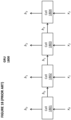
- Figure 14 depicts an exemplary LSTM 1400.
- LSTM 1400 in this example comprises cells 1401, 1402, 1403, and 1404.
- Cell 1401 receives input vector x 0 and generates output vector h 0 and cell state vector c 0 .
- Cell 1402 receives input vector x 1 , the output vector (hidden state) h 0 from cell 1401, and cell state c 0 from cell 1401 and generates output vector h 1 and cell state vector c 1 .
- Cell 1403 receives input vector x 2 , the output vector (hidden state) h 1 from cell 1402, and cell state c 1 from cell 1402 and generates output vector h 2 and cell state vector c 2 .
- Cell 1404 receives input vector x 3 , the output vector (hidden state) h 2 from cell 1403, and cell state c 2 from cell 1403 and generates output vector h 3 .
- Additional cells can be used, and an LSTM with four cells is merely an example.
- FIG 15 depicts an exemplary implementation of an LSTM cell 1500, which can be used for cells 1401, 1402, 1403, and 1404 in Figure 14 .
- LSTM cell 1500 receives input vector x(t), cell state vector c(t-1) from a preceding cell, and output vector h(t-1) from a preceding cell, and generates cell state vector c(t) and output vector h(t).
- LSTM cell 1500 comprises sigmoid function devices 1501, 1502, and 1503, each of which applies a number between 0 and 1 to control how much of each component in the input vector is allowed through to the output vector.
- LSTM cell 1500 also comprises tanh devices 1504 and 1505 to apply a hyperbolic tangent function to an input vector, multiplier devices 1506, 1507, and 1508 to multiply two vectors together, and addition device 1509 to add two vectors together.
- Output vector h(t) can be provided to the next LSTM cell in the system, or it can be accessed for other purposes.
- FIG. 16 depicts an LSTM cell 1600, which is an example of an implementation of LSTM cell 1500.
- LSTM cell 1600 For the reader's convenience, the same numbering from LSTM cell 1500 is used in LSTM cell 1600.
- Sigmoid function devices 1501, 1502, and 1503 and tanh device 1504 each comprise multiple VMM arrays 1601 and activation function blocks 1602.
- VMM arrays are particular useful in LSTM cells used in certain neural network systems.
- the multiplier devices 1506, 1507, and 1508 and the addition device 1509 are implemented in a digital manner or in an analog manner.
- the activation function blocks 1602 can be implemented in a digital manner or in an analog manner.
- LSTM cell 1600 An alternative to LSTM cell 1600 (and another example of an implementation of LSTM cell 1500) is shown in Figure 17 .
- sigmoid function devices 1501, 1502, and 1503 and tanh device 1504 share the same physical hardware (VMM arrays 1701 and activation function block 1702) in a time-multiplexed fashion.
- LSTM cell 1700 also comprises multiplier device 1703 to multiply two vectors together, addition device 1708 to add two vectors together, tanh device 1505 (which comprises activation function block 1702), register 1707 to store the value i(t) when i(t) is output from sigmoid function block 1702, register 1704 to store the value f(t) * c(t-1) when that value is output from multiplier device 1703 through multiplexor 1710, register 1705 to store the value i(t) * u(t) when that value is output from multiplier device 1703 through multiplexor 1710, and register 1706 to store the value o(t) * c ⁇ (t) when that value is output from multiplier device 1703 through multiplexor 1710, and multiplexor 1709.
- LSTM cell 1600 contains multiple sets of VMM arrays 1601 and respective activation function blocks 1602
- LSTM cell 1700 contains only one set of VMM arrays 1701 and activation function block 1702, which are used to represent multiple layers in the embodiment of LSTM cell 1700.
- LSTM cell 1700 will require less space than LSTM 1600, as LSTM cell 1700 will require 1/4 as much space for VMMs and activation function blocks compared to LSTM cell 1600.
- LSTM units will typically comprise multiple VMM arrays, each of which requires functionality provided by certain circuit blocks outside of the VMM arrays, such as a summer and activation function block and high voltage generation blocks. Providing separate circuit blocks for each VMM array would require a significant amount of space within the semiconductor device and would be somewhat inefficient. The embodiments described below therefore reduce the circuitry required outside of the VMM arrays themselves.
- GRUs are a gating mechanism in recurrent neural networks. GRUs are similar to LSTMs, except that GRU cells generally contain fewer components than an LSTM cell.
- FIG. 18 depicts an exemplary GRU 1800.
- GRU 1800 in this example comprises cells 1801, 1802, 1803, and 1804.
- Cell 1801 receives input vector x 0 and generates output vector h 0 .
- Cell 1802 receives input vector x 1 , the output vector h 0 from cell 1801 and generates output vector h 1 .
- Cell 1803 receives input vector x 2 and the output vector (hidden state) h 1 from cell 1802 and generates output vector h 2 .
- Cell 1804 receives input vector x 3 and the output vector (hidden state) h 2 from cell 1803 and generates output vector h 3 . Additional cells can be used, and an GRU with four cells is merely an example.
- FIG 19 depicts an exemplary implementation of a GRU cell 1900, which can be used for cells 1801, 1802, 1803, and 1804 of Figure 18 .
- GRU cell 1900 receives input vector x(t) and output vector h(t-1) from a preceding GRU cell and generates output vector h(t).
- GRU cell 1900 comprises sigmoid function devices 1901 and 1902, each of which applies a number between 0 and 1 to components from output vector h(t-1) and input vector x(t).
- GRU cell 1900 also comprises a tanh device 1903 to apply a hyperbolic tangent function to an input vector, a plurality of multiplier devices 1904, 1905, and 1906 to multiply two vectors together, an addition device 1907 to add two vectors together, and a complementary device 1908 to subtract an input from 1 to generate an output.
- a tanh device 1903 to apply a hyperbolic tangent function to an input vector
- a plurality of multiplier devices 1904, 1905, and 1906 to multiply two vectors together
- an addition device 1907 to add two vectors together
- a complementary device 1908 to subtract an input from 1 to generate an output.
- FIG. 20 depicts a GRU cell 2000, which is an example of an implementation of GRU cell 1900.
- GRU cell 1900 For the reader's convenience, the same numbering from GRU cell 1900 is used in GRU cell 2000.
- sigmoid function devices 1901 and 1902, and tanh device 1903 each comprise multiple VMM arrays 2001 and activation function blocks 2002.
- VMM arrays are of particular use in GRU cells used in certain neural network systems.
- the multiplier devices 1904, 1905, 1906, the addition device 1907, and the complementary device 1908 are implemented in a digital manner or in an analog manner.
- the activation function blocks 2002 can be implemented in a digital manner or in an analog manner.
- GRU cell 2000 (and another example of an implementation of CRU cell 1900) is shown in Figure 21 .
- GRU cell 2100 utilizes VMM arrays 2101 and activation function block 2102, which when configured as a sigmoid function applies a number between 0 and 1 to control how much of each component in the input vector is allowed through to the output vector.
- sigmoid function devices 1901 and 1902 and tanh device 1903 share the same physical hardware (VMM arrays 2101 and activation function block 2102) in a time-multiplexed fashion.
- GRU cell 2100 also comprises multiplier device 2103 to multiply two vectors together, addition device 2105 to add two vectors together, complementary device 2109 to subtract an input from 1 to generate an output, multiplexor 2104, register 2106 to hold the value h(t-1) * r(t) when that value is output from multiplier device 2103 through multiplexor 2104, register 2107 to hold the value h(t-1) *z(t) when that value is output from multiplier device 2103 through multiplexor 2104, and register 2108 to hold the value h ⁇ (t) * (1-z(t)) when that value is output from multiplier device 2103 through multiplexor 2104.
- GRU cell 2000 contains multiple sets of VMM arrays 2001 and activation function blocks 2002
- GRU cell 2100 contains only one set of VMM arrays 2101 and activation function block 2102, which are used to represent multiple layers in the embodiment of GRU cell 2100.
- GRU cell 2100 will require less space than GRU cell 2000, as GRU cell 2100 will require 1/3 as much space for VMMs and activation function blocks compared to GRU cell 2000.
- GRU systems will typically comprise multiple VMM arrays, each of which requires functionality provided by certain circuit blocks outside of the VMM arrays, such as a summer and activation function block and high voltage generation blocks. Providing separate circuit blocks for each VMM array would require a significant amount of space within the semiconductor device and would be somewhat inefficient. The embodiments described below therefore reduce the circuitry required outside of the VMM arrays themselves.
- the input to the VMM arrays can be an analog level, a binary level, a pulse, a time modulated pulse, or digital bits (in this case a DAC is needed to convert digital bits to appropriate input analog level) and the output can be an analog level, a binary level, a timing pulse, pulses, or digital bits (in this case an output ADC is needed to convert output analog level into digital bits).
- each weight W can be implemented by a single memory cell or by a differential cell or by two blend memory cells (average of 2 cells).
- the two blend memory cells two memory cells are needed to implement a weight W as an average of two cells.
- Figure 31 depicts VMM system 3100.
- W+ lines half of the bit lines are designated as W+ lines, that is, bit lines connecting to memory cells that will store positive weights W+
- W- lines half of the bit lines connecting to memory cells implementing negative weights W-.
- the W- lines are interspersed among the W+ lines in an alternating fashion.
- the subtraction operation is performed by a summation circuit that receives current from a W+ line and a W- line, such as summation circuits 3101 and 3102.
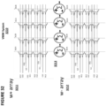
- FIG. 32 depicts another embodiment.
- positive weights W+ are implemented in first array 3211 and negative weights W- are implemented in a second array 3212, second array 3212 separate from the first array, and the resulting weights are appropriately combined together by summation circuits 3213.
- FIG. 33 depicts VMM system 3300.
- VMM system 3300 comprises array 3301 and array 3302.
- Half of the bit lines in each of array 3301 and 3302 are designated as W+ lines, that is, bit lines connecting to memory cells that will store positive weights W+
- the other half of the bit lines in each of array 3301 and 3302 are designated as W- lines, that is, bit lines connecting to memory cells implementing negative weights W-.
- the W- lines are interspersed among the W+ lines in an alternating fashion.
- the subtraction operation is performed by a summation circuit that receives current from a W+ line and a W- line, such as summation circuits 3303, 3304, 3305, and 3306.
- a summation circuit that receives current from a W+ line and a W- line, such as summation circuits 3303, 3304, 3305, and 3306.
- each W value from each array 3301 and 3302 can be further combined through summation circuits 3307 and 3308, such that each W value is the result of a W value from array 3301 minus a W value from array 3302, meaning that the end result from summation circuits 3307 and 3308 is a differential value of two differential values.
- Each non-volatile memory cells used in the analog neural memory system is to be erased and programmed to hold a very specific and precise amount of charge, i.e., the number of electrons, in the floating gate.
- each floating gate should hold one of N different values, where N is the number of different weights that can be indicated by each cell. Examples of N include 16, 32, 64, 128, and 256.
- a read operation should be able to accurately discern between N different levels.
- VMM systems There is a need in VMM systems for improved input blocks that can be used to quickly and accurately apply currents or voltages to one or more lines of rows of cells to be programmed, read, or erased.
- the present invention is defined in independent claim 1.
- Numerous embodiments of input circuitry for an analog neural memory in a deep learning artificial neural network are disclosed.
- the artificial neural networks of the present invention utilize a combination of CMOS technology and non-volatile memory arrays.
- FIG. 34 depicts a block diagram of VMM system 3400.
- VMM system 3400 comprises VMM array 3401, row decoder 3402, high voltage decoder 3403, column decoder 3404, bit line drivers 3405, input circuit 3406, output circuit 3407, control logic 3408, and bias generator 3409.
- VMM system 3400 further comprises high voltage generation block 3410, which comprises charge pump 3411, charge pump regulator 3412, and high voltage analog precision level generator 3413.
- VMM system 3400 further comprises (program/erase, or weight tuning) algorithm controller 3414, analog circuitry 3415, control engine 3416 (that may include special functions such as arithmetic functions, activation functions, embedded microcontroller logic, without limitation), and test control logic 3417.
- the systems and methods described below can be implemented in VMM system 3400.
- the input circuit 3406 may include circuits such as a DAC (digital to analog converter), DPC (digital to pulses converter, digital to time modulated pulse converter), AAC (analog to analog converter, such as a current to voltage converter, logarithmic converter ), PAC (pulse to analog level converter), or any other type of converters.
- the input circuit 3406 may implement normalization, linear or non-linear up/down scaling functions, or arithmetic functions.
- the input circuit 3406 may implement a temperature compensation function for input levels.
- the input circuit 3406 may implement an activation function such as ReLU or sigmoid.
- the output circuit 3407 may include circuits such as a ADC (analog to digital converter, to convert neuron analog output to digital bits), AAC (analog to analog converter, such as a current to voltage converter, logarithmic converter), APC (analog to pulse(s) converter, analog to time modulated pulse converter), or any other type of converters.
- the output circuit 3407 may implement an activation function such as rectified linear activation function (ReLU) or sigmoid.
- the output circuit 3407 may implement statistic normalization, regularization, up/down scaling/gain functions, statistical rounding, or arithmetic functions (e.g., add, subtract, divide, multiply, shift, log) for neuron outputs.
- the output circuit 3407 may implement a temperature compensation function for neuron outputs or array outputs (such as bitline output) so as to keep power consumption of the array approximately constant or to improve precision of the array (neuron) outputs such as by keeping the IV slope approximately the same.
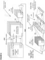
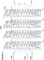
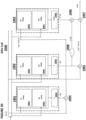
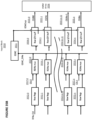
- Figure 35A depicts input block 3500 to be used to provide inputs to VMM array 3506.
- Input block 3500 comprises global digital-to-analog converter (DAC) 3501; row registers 3502-0 through 3502-n, each corresponding to a one of the rows numbered 0 through n in the array; digital comparator blocks 3503-0 through 3503-n; row sample-and-hold buffers 3504-0 through 3504-n, each corresponding to one of the rows numbered 0 through n; and output signals 3505-0 through 3505-n, each corresponding to one of the rows numbered 0 through n, and denoted CGINO, CGIN1..., CGINn-1 and CGINn, respectively.
- Signal GDACsup is the global DAC signal supplied by the global DAC 3501.
- the signals CGIN0-n couples to the row inputs of the array 3506.
- Digital comparator blocks 3503 compare the value stored in the associated row register 3502 against CLKCOUNTx, which is a result of counting a clock signal during an interval; if it matches, then the corresponding row S/H 3504 is enabled to sample the value from the global DAC 3501 into the respective row S/H buffer. This technique will be referred to as global row DAC sampling.
- Each row in VMM array 3506 has a corresponding row register 3502, digital comparator block 3503, and row S/H 3504.
- row registers 3502-0 through 3502-n are loaded with digital input bits DINx (where x is the number of bits, such as 8 or 16 bits) for that particular row and receives a clock signal, CLK.
- the CLK signal is used to load in the data from the DINx into the row registers 3502-x.
- Global digital-to-analog converter 3501 is shared by all rows, and in a time-multiplexed fashion, performs a digital-to-analog conversion on the digital bits DINx stored in a particular row register 3502. The conversion is done by comparing the digital input bits of a particular row versus CLKCOUNTx, which is digital counting value, by each of the digital comparator blocks 3503).
- Output signal 3504 can be applied, for example, to a control gate line or a word line during a programming operation in that particular row, in the manner described above with respect to other Figures.
- the row sample-and-hold buffer 3504 can be shared between multiple rows by time multiplexing the row sample-and-hold buffers.
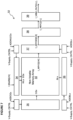
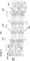
- Figure 35B depicts input block 3550 to be used to provide inputs to VMM array 3556.
- Input block 3550 comprises global digital-to-analog converter (DAC) 3551; row registers 3552-0 through 3552-n, each corresponding to a respective one of the rows numbered 0 through n in the VMM array; digital multiplexer (mux) blocks 3553-0 through 3553-n, each corresponding to a respective one of the rows numbered 0 through n; row sample-and-hold (S/H) buffers 3553-0 through 3553-n, each corresponding to a respective one of the rows numbered 0 through n; and output signals 3554-0 through 3554-n, denoted CGINO, CGIN1..., CGINn-1 and CGINn, respectively, each corresponding to a respective one of the rows numbered 0 through n.
- DAC digital-to-analog converter
- the digital mux blocks 3553 are used to multiplex out the data of the row registers 3552 into the bus GDAC_DINx, which is applied as an input to the global DAC 3551.
- the corresponding row S/H buffer samples the value from the global DAC into the local S/H.
- Each row has its own row register 3552, S/H buffer 3553m and output signal 3554.
- row registers 3552-0 through 3552-n are loaded with digital input bits DINx (where x is the number of bits, such as 8 or 16 bits) for that particular row and receives a clock signal, CLK.
- CLK clock signal
- the CLK signal is used to load in the data from the DINx into the row registers 3552-x.
- Global digital-to-analog converter 3551 is shared by all rows, and in a time-multiplexed fashion, performs a digital-to-analog conversion on the digital bits DINx stored in a particular row register 3552. The conversion is done by multiplexing the data of the row registers into the data input (bus GDAC_DINx) of the global DAC 3551.
- the multiplexing of the row register data into the data input bus GDAC_DINx is enabled by the signal EN-x 3557-x for each row.
- the corresponding row sample-and-hold buffer 3554 samples the analog output from global digital-to-analog converter 3551 and holds that value, which is then applied as output signal 3555 for that particular row.
- Output signal 3555 can be applied, for example, to a control gate line or a word line during a programming operation in that particular row, in the manner described above with respect to other Figures.
- the row sample-and-hold buffer 35554 can be shared between multiple rows by time multiplexing the row sample-and-hold buffers.
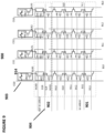
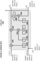
- Figure 36 depicts input block 3600 to be used to provide inputs to VMM array 3606.
- Input block 3600 is similar to input block 3500 but also provides a row decoder function to select one or more rows for an operation.
- Input block 3600 comprises global digital-to-analog converter and row decoder 3601; row registers 3602-0 through 3602-n, each corresponding to a respective one of the rows numbered 0 through n in the VMM array; digital comparator blocks 3603 through 3603-n each corresponding to a respective one of the rows numbered 0 through n in the VMM array; row sample-and-hold buffers 3604-0 through 3604-n; and output signals 3605-0 through 3605-n, denoted CGINO, CGIN1..., CGINn-1 and CGINn, respectively, each corresponding to a respective one of the rows numbered 0 through n.
- the digital comparator blocks 3603 compare the value stored in the respective row register 3602 against CLKCOUNTx, which is a counting value. When the digital counting values of the global DAC 3501 match the contents of the respective row register 3602. the respective row S/H buffer 3604 samples the value from the global DAC 3601 into the respective S/H buffer 3604. Each row has its own row register 3602, digital comparator block 3603, and row S/H buffer 3604.
- row registers 3602-0 through 3602-n are loaded with digital input bits DINx (where x is the number of bits, such as 8 or 16 bits) for the associated row and receives a clock signal, CLK.
- the CLK signal is used to load in the data from the DINx into the row registers 3602-x.
- Global digital-to-analog converter a 3601 (which consists of a plurality of global digital-to-analog converters, such as 3601-0 and 3601-1) is shared by all rows.
- global DAC 3601-0 operates on even rows and global DAC and row decoder 3601-1 operates on odd rows.
- Global digital-to-analog converter 3601 receives a row addresses through the row data-in bus GDAC_DINx and selects the corresponding ( rows. It then performs a digital-to-analog conversion on the digital bits DINx stored in the relevant row register(s) 3602 (through the GDAC_DINx bus).
- the corresponding row(s) sample-and-hold buffer 3604 for that row(s) samples the analog output from global digital-to-analog converter 3601 and holds that value, which is then applied as output signal 3605 for that particular row.
- Output signal 3605 can be applied, for example, to a control gate line or a word line during a programming operation in that particular row or rows, in the manner described above with respect to other Figures.
- Figure 37A depicts waveforms 3700 that illustrate exemplary linear voltage levels for exemplary sample-and-hold actions by row sample-and-hold buffer 3504 in Figure 35A , row sample-and-hold buffer 3554 in Figure 35B or row sample-and-hold buffer 3604 in Figure 36 .
- the signal GDACsup 3701 is the supplied voltage from the global linear DAC such as from the circuit blocks 3501 in Fig 35A , 3551 in Fig 35B , 3601x in Fig 36 . It shows the linear steps to illustrate this is a linear DAC.
- Figure 37B depicts waveforms 3720 that illustrate exemplary logarithmic voltage levels for exemplary sample-and-hold actions by row sample-and-hold buffer 3504 in Figure 35A , row sample-and-hold buffer 3554 in Figure 35B or row sample-and-hold buffer 3604 in Figure 36 .
- This is suitable for memory cells operating in sub threshold region.
- the global DAC voltage waveform can be done for memory cells operating in saturation region.
- the signal GDACsup 3721 is the supplied voltage from the global (sub threshold, linear, saturation) DAC such as from the circuit blocks 3501 in Fig 35A , 3551 in Fig 35B , 3601x in Fig 36 . It shows the log steps to illustrate this is a log DAC.
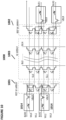
- Figure 38 depicts sample-and-hold buffer 3800, which can be used for row sample-and-hold buffer 3504 in Figure 35A , row sample-and-hold buffer 3554 in Figure 35B , or row sample-and-hold buffer 3604 in Figure 36 .
- Sample-and-hold buffer 3800 comprises switch 3801, capacitor 3802, and buffer 3803, the buffer 3803 can be done as a unity buffer using an operation amplifier.
- switch 3801 is closed (enabled, such as by the true result of the comparison of the digital comparator and the digital counting values), which allows an analog value (global DAC value) to be stored (held) in capacitor 3802.
- a value reflective of that stored value can then be output from buffer 3803 which drives a respective row input of the array.
- Capacitor 3802 can be an actual capacitor, or it can be an intrinsic capacitance found in a wire, for example.
- Sample-and-hold buffer 3900 comprises switch 3901 and capacitor 3902.
- switch 3901 is closed (enabled, such as by the true result of the comparison of the digital comparator and the digital counting value), which allows an analog value to be stored (held) in capacitor 3902.
- a value reflective of that value can then be output from capacitor 3902.
- Capacitor 3902 can be an actual capacitor, or it can be an intrinsic capacitance found in a wire, for example.
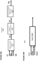
- Figure 40A depicts input block 4000.
- Input block 4000 comprises digital-to-analog converter 4001, voltage-to-current converter 4002, and current to voltage logarithmic converter 4003.
- Input block 4000 can be added to any of the preceding input blocks when it is desired to have an input voltage that varies according to a logarithmic function, which is useful, for example, if the memory cells in a VMM array are operating in the sub-threshold range.
- Digital-to-analog converter receives a digital input, DINx, and generates an analog voltage, Vout.
- Voltage-to-current converter 4002 linearly converts analog voltage Vout into a current Iout.
- the input block 4000 can be used as a global DAC as in Figure 35A , 35B and 36 . It can generate waveforms 3720 shown in Figure 37B .
- CLK is used to generate the DAC output voltages in a stepwise fashion from for example 0 to 256 steps for 8bit DAC.
- DINx is used to generate the DAC output voltage.
- Figure 40B depicts input block 4020.
- Input block 4020 comprises a digital-to-analog converter, which can be used as the global DAC. This can be used for example for memory cells operating in linear region.
- the input block 4020 can be used as a global DAC as in Figure 35 and 36 . It can generate waveforms 3700 shown in Figure 37A ,
- Figure 41A depicts input block 4100.
- Input block 4100 comprises current digital-to-analog converter 4101 and current to voltage logarithmic converter 4102.
- Input block 4100 can be added to any of the preceding input blocks when it is desired to have an input voltage that varies according to a logarithmic function, which is useful, for example, if the memory cells in a VMM array are operating in the sub-threshold range.
- Current digital-to-analog converter 4101 receives a digital input, DINx, as in previous examples and generates an analog current, Iout.
- Figure 41B depicts input block 4120.
- Input block 4120 comprises current digital-to-analog converter 4121 and current to voltage linear converter 4122.
- Input block 4120 can be added to any of the preceding input blocks when it is desired to have an input voltage that varies according to a linear function, which is useful, for example, if the memory cells in a VMM array are operating in the linear range.
- Current digital-to-analog converter 4121 receives a digital input, DINx, as in previous examples and generates an analog current, Iout.
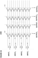
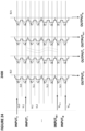
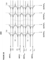
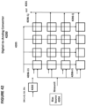
- Adjustable 2D thermometer code current digital-to-analog converter 4200 comprises control logic 4202 and 2D array 4205 comprising an array of i rows and j columns of devices 4206, where a particular device 4206 is noted by the label 4206-(row)(column).
- the particular devices 4206 may be current mirrors. As shown, there are 16 current mirrors (devices 4206) in the 2D array 4205.
- the adjustable 2D thermometer code current digital-to-analog converter 4200 converts a 4 digital input code into an output current 4201, Iout, with value from 1 to 16 times Ibiasunit which is provided from the bias source 4204.
- bias source 4204 can provide a current Ibiasunit of 1nA, which is mirrored into devices 4206.
- the first row consists of devices 4206-11 to 4206-1j and is enabled sequentially from left to right, one device 4206 at a time. Then the next row is enabled in a sequential manner from left to right to add to the first row, meaning 5 then 6 then 7 then 8 devices 4206 are enabled.
- any transistor mismatch associated with conventional binary decoding can be reduced.
- the sum of the enabled devices 4206 is then output as an output current 4201.
- the shown 4 x 4 2D thermometer code current digital-to-analog converter 4200 could be any other dimension such as 32 x 32 or 8 x 32.
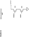
- Figure 43 depicts reference sub-circuit 4300, which is can be used for device 4206 in Figure 42 .
- Reference sub-circuit 4300 comprises NMOS transistors 4301 and 4302, configured as shown.
- the transistor 4302 is a current mirror bias transistor and transistor 4301 is an enabling transistor (to enable the bias transistor 4302 to be connected to output node OUTPUT), master bias current that is used to mirror to the transistor 4302 is not shown.
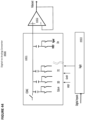
- Figure 44 depicts a SAR (successive approximation register) digital -to-analog converter 4400.
- This circuit is a digital -to-analog converter that relies upon charge redistribution using binary capacitors. It includes a binary CDAC (DAC basing on capacitors) 4401, op-amp/comparator 4402, and SAR logic 4403.
- GndV is a low voltage reference level, for example, ground level. This is, for example, used in Figures 40A and 40B .
- Figure 45 depicts voltage-to-current converter 4500, which comprises op amp 4501, NMOS transistor 4501, and resistor 4503, configured as shown.
- Voltage-to-current converter 4500 receives input voltage VIN and generates output current IOUT. This, for example, can be used in combination with DAC circuit 4400 to convert voltage into current. This current can be used to convert to a voltage using a log I to V converter such as in Fig 46 / 47 / 48 .
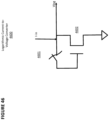
- Figure 46 depicts logarithmic current-to-voltage converter 4600.
- Logarithmic current-to-voltage converter 4600 comprises switch 4601 and NMOS transistor 4602, configured as shown.
- the NMOS 4602 operates in the sub-threshold region.
- Logarithmic current-to-voltage converter 4600 receives input I-in and generates output Vlog.
- Figure 47 depicts logarithmic current-to-voltage converter 4700.
- Logarithmic current-to-voltage converter 4700 comprises switches 4701 and 4702 and memory cell 4703, configured as shown.
- the memory cell 4703 operates in the sub-threshold region.
- Logarithmic current-to-voltage converter 4600 receives input I-in and generates output Vlog.
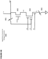
- Figure 48 depicts logarithmic current-to-voltage converter 4800.
- Logarithmic current-to-voltage converter 4800 comprises switches 4801 and 4802, NMOS transistor 4803, and memory cell 4804, configured as shown.
- the memory cell 4804 operates in the sub-threshold region.
- the transistor 4803 imposes a constant bias on the drain of memory cell 4804.
- Logarithmic current-to-voltage converter 4600 receives input I-in and generates output Vlog.
- the log I to V conversion is done to replicate the log I vs V slope of the memory cell current.
- K is determined by the floating charge in the memory cell, which basically represents the weight in neural network.
- the term “adjacent” includes “directly adjacent” (no intermediate materials, elements or space disposed therebetween) and “indirectly adjacent” (intermediate materials, elements or space disposed there between), “mounted to” includes “directly mounted to” (no intermediate materials, elements or space disposed there between) and “indirectly mounted to” (intermediate materials, elements or spaced disposed there between), and “electrically coupled” includes “directly electrically coupled to” (no intermediate materials or elements there between that electrically connect the elements together) and “indirectly electrically coupled to” (intermediate materials or elements there between that electrically connect the elements together).
- forming an element "over a substrate” can include forming the element directly on the substrate with no intermediate materials/elements therebetween, as well as forming the element indirectly on the substrate with one or more intermediate materials/elements there between.
Landscapes
- Engineering & Computer Science (AREA)
- Physics & Mathematics (AREA)
- Theoretical Computer Science (AREA)
- Biomedical Technology (AREA)
- Health & Medical Sciences (AREA)
- Life Sciences & Earth Sciences (AREA)
- General Physics & Mathematics (AREA)
- Mathematical Physics (AREA)
- Biophysics (AREA)
- Data Mining & Analysis (AREA)
- Molecular Biology (AREA)
- General Health & Medical Sciences (AREA)
- Computing Systems (AREA)
- Software Systems (AREA)
- General Engineering & Computer Science (AREA)
- Computational Linguistics (AREA)
- Artificial Intelligence (AREA)
- Evolutionary Computation (AREA)
- Neurology (AREA)
- Computer Hardware Design (AREA)
- Pure & Applied Mathematics (AREA)
- Mathematical Optimization (AREA)
- Mathematical Analysis (AREA)
- Computational Mathematics (AREA)
- Databases & Information Systems (AREA)
- Algebra (AREA)
- Non-Volatile Memory (AREA)
- Analogue/Digital Conversion (AREA)
- Read Only Memory (AREA)
- Complex Calculations (AREA)
- Semiconductor Memories (AREA)
Claims (7)
- Eingabeblock zum Bereitstellen einer Eingabe für ein Vektor-Matrix-Multiplikationsarray in einem neuronalen Speichersystem, das Vektor-Matrix-Multiplikationsarray umfassend nichtflüchtige Speicherzellen, die in Zeilen und Spalten angeordnet sind, und der Eingabeblock umfassend:einen globalen Digital-Analog-Umsetzer;eine Vielzahl von Zeilenabtast-and-Haltepuffern, wobei jeder Zeilenabtast-und-Haltepuffer einer Zeile in dem Array entspricht;dadurch gekennzeichnet, dass der Eingabeblock ferner umfassteine Vielzahl von Zeilenregistern, wobei jedes Zeilenregister einer Zeile in dem Array entspricht; undwobei, wenn eine Zeile ausgewählt wird, der globale Digital-Analog-Umsetzer einen in einem Zeilenregister gespeicherten digitalen Wert, der der ausgewählten Zeile entspricht, in einen analogen Wert umwandelt, der durch den Zeilenabtast- und Haltepuffer, der der ausgewählten Zeile entspricht, abgetastet und gehalten und an eine Leitung angelegt wird, die mit der ausgewählten Zeile gekoppelt ist.
- Eingabeblock nach Anspruch 1, wobei der globale Digital-Analog-Umsetzer einen linearen Digital-Analog-Umsetzer umfasst.
- Eingabeblock nach Anspruch 1, wobei der globale Digital-Analog-Umsetzer einen logarithmischen Digital-Analog-Umsetzer umfasst.
- Eingabeblock nach Anspruch 1, wobei der globale Digital-Analog-Umsetzer einen Digital-Analog-Umsetzer für ungerade Zeilen und einen weiteren Digital-Analog-Umsetzer für gerade Zeilen umfasst.
- Eingabeblock nach Anspruch 1, wobei der globale Digital-Analog-Umsetzer einen Zeilendecoder umfasst, der die ausgewählte Zeile als Reaktion auf eine Zeilenadresse auswählt.
- Eingabeblock nach Anspruch 1, wobei jeder Zeilenabtast-und-Haltepuffer einen Schalter und einen Kondensator umfasst, wobei wenn der Schalter geschlossen ist, er einen analogen Eingang an den Kondensator anlegt.
- Eingabeblock nach Anspruch 6, wobei jeder Zeilenabtast-und-Haltepuffer ferner einen Puffer zum Ausgeben eines Werts umfasst, der einen in dem Kondensator gespeicherten Wert widerspiegelt.
Priority Applications (1)
| Application Number | Priority Date | Filing Date | Title |
|---|---|---|---|
| EP25166189.8A EP4553838A3 (de) | 2021-08-02 | 2021-11-13 | Eingangsschaltung für analogen neuronalen speicher in einem künstlichen neuronalen tiefenlernnetz |
Applications Claiming Priority (3)
| Application Number | Priority Date | Filing Date | Title |
|---|---|---|---|
| US202163228570P | 2021-08-02 | 2021-08-02 | |
| US17/520,396 US12579422B2 (en) | 2021-08-02 | 2021-11-05 | Input circuitry for analog neural memory in a deep learning artificial neural network |
| PCT/US2021/059285 WO2023014387A1 (en) | 2021-08-02 | 2021-11-13 | Input circuitry for analog neural memory in a deep learning artificial neural network |
Related Child Applications (2)
| Application Number | Title | Priority Date | Filing Date |
|---|---|---|---|
| EP25166189.8A Division EP4553838A3 (de) | 2021-08-02 | 2021-11-13 | Eingangsschaltung für analogen neuronalen speicher in einem künstlichen neuronalen tiefenlernnetz |
| EP25166189.8A Division-Into EP4553838A3 (de) | 2021-08-02 | 2021-11-13 | Eingangsschaltung für analogen neuronalen speicher in einem künstlichen neuronalen tiefenlernnetz |
Publications (2)
| Publication Number | Publication Date |
|---|---|
| EP4381502A1 EP4381502A1 (de) | 2024-06-12 |
| EP4381502B1 true EP4381502B1 (de) | 2025-06-18 |
Family
ID=78829604
Family Applications (2)
| Application Number | Title | Priority Date | Filing Date |
|---|---|---|---|
| EP21823704.8A Active EP4381502B1 (de) | 2021-08-02 | 2021-11-13 | Eingangsschaltung für analogen neuronalen speicher in einem künstlichen neuronalen tiefenlernnetz |
| EP25166189.8A Pending EP4553838A3 (de) | 2021-08-02 | 2021-11-13 | Eingangsschaltung für analogen neuronalen speicher in einem künstlichen neuronalen tiefenlernnetz |
Family Applications After (1)
| Application Number | Title | Priority Date | Filing Date |
|---|---|---|---|
| EP25166189.8A Pending EP4553838A3 (de) | 2021-08-02 | 2021-11-13 | Eingangsschaltung für analogen neuronalen speicher in einem künstlichen neuronalen tiefenlernnetz |
Country Status (6)
| Country | Link |
|---|---|
| US (1) | US12579422B2 (de) |
| EP (2) | EP4381502B1 (de) |
| JP (2) | JP7733207B2 (de) |
| KR (2) | KR102840751B1 (de) |
| TW (2) | TW202533093A (de) |
| WO (1) | WO2023014387A1 (de) |
Families Citing this family (3)
| Publication number | Priority date | Publication date | Assignee | Title |
|---|---|---|---|---|
| WO2025042426A1 (en) * | 2023-08-24 | 2025-02-27 | Silicon Storage Technology, Inc. | Input block for vector-by-matrix multiplication array |
| WO2025122550A1 (en) * | 2023-12-04 | 2025-06-12 | Encharge Ai, Inc. | Systems and methods for input reference generation technique for in-memory computing array |
| KR102885665B1 (ko) * | 2024-06-10 | 2025-11-13 | 울산과학기술원 | 삼진 신경망을 이용한 연산 장치 및 연산 방법, 삼진 신경망을 이용한 연산 장치를 포함하는 아날로그 신호 분석 시스템 |
Family Cites Families (18)
| Publication number | Priority date | Publication date | Assignee | Title |
|---|---|---|---|---|
| JP2831076B2 (ja) * | 1990-01-19 | 1998-12-02 | 松下電器産業株式会社 | ニューロコンピュータ |
| US5029130A (en) | 1990-01-22 | 1991-07-02 | Silicon Storage Technology, Inc. | Single transistor non-valatile electrically alterable semiconductor memory device |
| JP2001339258A (ja) * | 2000-05-24 | 2001-12-07 | Thine Electronics Inc | 電圧電流変換回路 |
| WO2003049024A1 (en) * | 2001-10-09 | 2003-06-12 | Magtek, Inc. | Method and apparatus for generating images of magnetic fields in at least two dimensions |
| JP4060084B2 (ja) | 2002-01-29 | 2008-03-12 | カルソニックコンプレッサー株式会社 | 気体圧縮機 |
| US6747310B2 (en) | 2002-10-07 | 2004-06-08 | Actrans System Inc. | Flash memory cells with separated self-aligned select and erase gates, and process of fabrication |
| US9792744B2 (en) | 2015-06-01 | 2017-10-17 | Schlage Lock Company Llc | Antenna diversity implementation for wireless locks |
| KR102182583B1 (ko) | 2016-05-17 | 2020-11-24 | 실리콘 스토리지 테크놀로지 인크 | 비휘발성 메모리 어레이를 사용하는 딥러닝 신경망 분류기 |
| US11087207B2 (en) * | 2018-03-14 | 2021-08-10 | Silicon Storage Technology, Inc. | Decoders for analog neural memory in deep learning artificial neural network |
| US10748630B2 (en) | 2017-11-29 | 2020-08-18 | Silicon Storage Technology, Inc. | High precision and highly efficient tuning mechanisms and algorithms for analog neuromorphic memory in artificial neural networks |
| US10891080B1 (en) | 2018-06-04 | 2021-01-12 | Mentium Technologies Inc. | Management of non-volatile memory arrays |
| US10755783B2 (en) * | 2018-08-27 | 2020-08-25 | Silicon Storage Technology | Temperature and leakage compensation for memory cells in an analog neural memory system used in a deep learning neural network |
| US11893478B2 (en) * | 2019-01-18 | 2024-02-06 | Silicon Storage Technology, Inc. | Programmable output blocks for analog neural memory in a deep learning artificial neural network |
| US11500442B2 (en) * | 2019-01-18 | 2022-11-15 | Silicon Storage Technology, Inc. | System for converting neuron current into neuron current-based time pulses in an analog neural memory in a deep learning artificial neural network |
| US11423979B2 (en) * | 2019-04-29 | 2022-08-23 | Silicon Storage Technology, Inc. | Decoding system and physical layout for analog neural memory in deep learning artificial neural network |
| JP7034984B2 (ja) | 2019-05-30 | 2022-03-14 | 株式会社東芝 | 演算装置 |
| US11431347B2 (en) | 2019-12-09 | 2022-08-30 | Technion Research & Development Foundation Limited | Analog-to-digital converter using a pipelined memristive neural network |
| DE102021105181A1 (de) * | 2020-04-30 | 2021-11-04 | Taiwan Semiconductor Manufacturing Co., Ltd. | Vorrichtung und verfahren zum lesen von daten in einem speicher |
-
2021
- 2021-11-05 US US17/520,396 patent/US12579422B2/en active Active
- 2021-11-13 JP JP2024501687A patent/JP7733207B2/ja active Active
- 2021-11-13 EP EP21823704.8A patent/EP4381502B1/de active Active
- 2021-11-13 KR KR1020247002512A patent/KR102840751B1/ko active Active
- 2021-11-13 KR KR1020257025114A patent/KR20250117479A/ko active Pending
- 2021-11-13 EP EP25166189.8A patent/EP4553838A3/de active Pending
- 2021-11-13 WO PCT/US2021/059285 patent/WO2023014387A1/en not_active Ceased
-
2022
- 2022-07-25 TW TW114114699A patent/TW202533093A/zh unknown
- 2022-07-25 TW TW111127683A patent/TWI884383B/zh active
-
2025
- 2025-08-21 JP JP2025138408A patent/JP2025187037A/ja active Pending
Also Published As
| Publication number | Publication date |
|---|---|
| TWI884383B (zh) | 2025-05-21 |
| US20230048411A1 (en) | 2023-02-16 |
| KR20250117479A (ko) | 2025-08-04 |
| EP4553838A3 (de) | 2025-09-24 |
| TW202533093A (zh) | 2025-08-16 |
| KR20240026194A (ko) | 2024-02-27 |
| JP2025187037A (ja) | 2025-12-24 |
| KR102840751B1 (ko) | 2025-08-05 |
| WO2023014387A1 (en) | 2023-02-09 |
| JP7733207B2 (ja) | 2025-09-02 |
| EP4553838A2 (de) | 2025-05-14 |
| US12579422B2 (en) | 2026-03-17 |
| JP2024532008A (ja) | 2024-09-04 |
| TW202314599A (zh) | 2023-04-01 |
| EP4381502A1 (de) | 2024-06-12 |
Similar Documents
| Publication | Publication Date | Title |
|---|---|---|
| EP4202769B1 (de) | Analoges neuronales speichersystem für ein tiefenlernendes neuronales netz mit mehreren vektor-x-matrix-multiplikationsfeldern und gemeinsamen komponenten | |
| EP3867911B1 (de) | Präzisionsabstimmung für die programmierung eines analogen neuronalen speichers in einem künstlichen neuronalen tiefenlernnetz | |
| EP3918601B1 (de) | Präzisionsprogrammierschaltung für einen analogen neuronalen speicher in einem künstlichen neuronalen netzwerk mit tiefenlernen | |
| EP4341933B1 (de) | Ausgangsschaltung für analogen neuronalen speicher in einem künstlichen neuronalen tiefenlernnetz | |
| EP4381502B1 (de) | Eingangsschaltung für analogen neuronalen speicher in einem künstlichen neuronalen tiefenlernnetz | |
| KR20240148895A (ko) | 아날로그 출력을 활용한 벡터와 행렬 간 승산 어레이 | |
| WO2022245384A1 (en) | Output circuit for analog neural memory in a deep learning artificial neural network | |
| EP4381504B1 (de) | Ausgangsschaltung für analogen neuronalen speicher in einem künstlichen neuronalen tiefenlernnetz | |
| EP4341934B1 (de) | Geteilte arrayarchitektur für analogen neuronalen speicher in einem künstlichen neuronalen tiefenlernnetz | |
| US20220374696A1 (en) | Split array architecture for analog neural memory in a deep learning artificial neural network | |
| US20230325649A1 (en) | Vector-by-matrix-multiplication array utilizing analog inputs | |
| EP4659149A1 (de) | Strom-spannungswandler mit gleichtaktschaltung | |
| EP4385016B1 (de) | Hybrides speichersystem, das zur speicherung von gewichtsdaten eines neuronalen speichers in analoger oder digitaler form konfiguriert werden kann | |
| EP4469940B1 (de) | Künstliches neuronales netzwerk mit einem analogen array und einem digitalen array | |
| US12608137B2 (en) | Redundancy for an array of non-volatile memory cells using tag registers | |
| US20250068900A1 (en) | Output circuit for a vector-by-matrix multiplication array | |
| WO2023196000A1 (en) | Vector-by-matrix-multiplication array utilizing analog inputs | |
| WO2025111009A1 (en) | Sigma-delta analog-to-digital converter to generate digital output from vector-by-matrix multiplication array | |
| WO2024215346A1 (en) | Masking sparse inputs and outputs in neural network array | |
| CN117716427A (zh) | 用于深度学习人工神经网络中的模拟神经存储器的输入电路 |
Legal Events
| Date | Code | Title | Description |
|---|---|---|---|
| STAA | Information on the status of an ep patent application or granted ep patent |
Free format text: STATUS: UNKNOWN |
|
| STAA | Information on the status of an ep patent application or granted ep patent |
Free format text: STATUS: THE INTERNATIONAL PUBLICATION HAS BEEN MADE |
|
| PUAI | Public reference made under article 153(3) epc to a published international application that has entered the european phase |
Free format text: ORIGINAL CODE: 0009012 |
|
| STAA | Information on the status of an ep patent application or granted ep patent |
Free format text: STATUS: REQUEST FOR EXAMINATION WAS MADE |
|
| 17P | Request for examination filed |
Effective date: 20240226 |
|
| AK | Designated contracting states |
Kind code of ref document: A1 Designated state(s): AL AT BE BG CH CY CZ DE DK EE ES FI FR GB GR HR HU IE IS IT LI LT LU LV MC MK MT NL NO PL PT RO RS SE SI SK SM TR |
|
| DAV | Request for validation of the european patent (deleted) | ||
| DAX | Request for extension of the european patent (deleted) | ||
| GRAP | Despatch of communication of intention to grant a patent |
Free format text: ORIGINAL CODE: EPIDOSNIGR1 |
|
| STAA | Information on the status of an ep patent application or granted ep patent |
Free format text: STATUS: GRANT OF PATENT IS INTENDED |
|
| INTG | Intention to grant announced |
Effective date: 20250107 |
|
| GRAS | Grant fee paid |
Free format text: ORIGINAL CODE: EPIDOSNIGR3 |
|
| GRAA | (expected) grant |
Free format text: ORIGINAL CODE: 0009210 |
|
| STAA | Information on the status of an ep patent application or granted ep patent |
Free format text: STATUS: THE PATENT HAS BEEN GRANTED |
|
| P01 | Opt-out of the competence of the unified patent court (upc) registered |
Free format text: CASE NUMBER: APP_21522/2025 Effective date: 20250506 |
|
| AK | Designated contracting states |
Kind code of ref document: B1 Designated state(s): AL AT BE BG CH CY CZ DE DK EE ES FI FR GB GR HR HU IE IS IT LI LT LU LV MC MK MT NL NO PL PT RO RS SE SI SK SM TR |
|
| REG | Reference to a national code |
Ref country code: GB Ref legal event code: FG4D |
|
| REG | Reference to a national code |
Ref country code: CH Ref legal event code: EP |
|
| REG | Reference to a national code |
Ref country code: DE Ref legal event code: R096 Ref document number: 602021032556 Country of ref document: DE |
|
| REG | Reference to a national code |
Ref country code: CH Ref legal event code: EP |
|
| REG | Reference to a national code |
Ref country code: IE Ref legal event code: FG4D |
|
| REG | Reference to a national code |
Ref country code: NL Ref legal event code: FP |
|
| PG25 | Lapsed in a contracting state [announced via postgrant information from national office to epo] |
Ref country code: FI Free format text: LAPSE BECAUSE OF FAILURE TO SUBMIT A TRANSLATION OF THE DESCRIPTION OR TO PAY THE FEE WITHIN THE PRESCRIBED TIME-LIMIT Effective date: 20250618 |
|
| REG | Reference to a national code |
Ref country code: LT Ref legal event code: MG9D |
|
| PG25 | Lapsed in a contracting state [announced via postgrant information from national office to epo] |
Ref country code: GR Free format text: LAPSE BECAUSE OF FAILURE TO SUBMIT A TRANSLATION OF THE DESCRIPTION OR TO PAY THE FEE WITHIN THE PRESCRIBED TIME-LIMIT Effective date: 20250919 Ref country code: NO Free format text: LAPSE BECAUSE OF FAILURE TO SUBMIT A TRANSLATION OF THE DESCRIPTION OR TO PAY THE FEE WITHIN THE PRESCRIBED TIME-LIMIT Effective date: 20250918 |
|
| PG25 | Lapsed in a contracting state [announced via postgrant information from national office to epo] |
Ref country code: BG Free format text: LAPSE BECAUSE OF FAILURE TO SUBMIT A TRANSLATION OF THE DESCRIPTION OR TO PAY THE FEE WITHIN THE PRESCRIBED TIME-LIMIT Effective date: 20250618 |
|
| PG25 | Lapsed in a contracting state [announced via postgrant information from national office to epo] |
Ref country code: HR Free format text: LAPSE BECAUSE OF FAILURE TO SUBMIT A TRANSLATION OF THE DESCRIPTION OR TO PAY THE FEE WITHIN THE PRESCRIBED TIME-LIMIT Effective date: 20250618 |
|
| PG25 | Lapsed in a contracting state [announced via postgrant information from national office to epo] |
Ref country code: RS Free format text: LAPSE BECAUSE OF FAILURE TO SUBMIT A TRANSLATION OF THE DESCRIPTION OR TO PAY THE FEE WITHIN THE PRESCRIBED TIME-LIMIT Effective date: 20250918 |
|
| PG25 | Lapsed in a contracting state [announced via postgrant information from national office to epo] |
Ref country code: LV Free format text: LAPSE BECAUSE OF FAILURE TO SUBMIT A TRANSLATION OF THE DESCRIPTION OR TO PAY THE FEE WITHIN THE PRESCRIBED TIME-LIMIT Effective date: 20250618 |
|
| PGFP | Annual fee paid to national office [announced via postgrant information from national office to epo] |
Ref country code: NL Payment date: 20251022 Year of fee payment: 5 |
|
| PG25 | Lapsed in a contracting state [announced via postgrant information from national office to epo] |
Ref country code: PT Free format text: LAPSE BECAUSE OF FAILURE TO SUBMIT A TRANSLATION OF THE DESCRIPTION OR TO PAY THE FEE WITHIN THE PRESCRIBED TIME-LIMIT Effective date: 20251020 |
|
| REG | Reference to a national code |
Ref country code: AT Ref legal event code: MK05 Ref document number: 1804997 Country of ref document: AT Kind code of ref document: T Effective date: 20250618 |
|
| PG25 | Lapsed in a contracting state [announced via postgrant information from national office to epo] |
Ref country code: IS Free format text: LAPSE BECAUSE OF FAILURE TO SUBMIT A TRANSLATION OF THE DESCRIPTION OR TO PAY THE FEE WITHIN THE PRESCRIBED TIME-LIMIT Effective date: 20251018 |
|
| PGFP | Annual fee paid to national office [announced via postgrant information from national office to epo] |
Ref country code: DE Payment date: 20251022 Year of fee payment: 5 |
|
| PG25 | Lapsed in a contracting state [announced via postgrant information from national office to epo] |
Ref country code: AT Free format text: LAPSE BECAUSE OF FAILURE TO SUBMIT A TRANSLATION OF THE DESCRIPTION OR TO PAY THE FEE WITHIN THE PRESCRIBED TIME-LIMIT Effective date: 20250618 Ref country code: SM Free format text: LAPSE BECAUSE OF FAILURE TO SUBMIT A TRANSLATION OF THE DESCRIPTION OR TO PAY THE FEE WITHIN THE PRESCRIBED TIME-LIMIT Effective date: 20250618 |
|
| PGFP | Annual fee paid to national office [announced via postgrant information from national office to epo] |
Ref country code: FR Payment date: 20251022 Year of fee payment: 5 |
|
| PG25 | Lapsed in a contracting state [announced via postgrant information from national office to epo] |
Ref country code: CZ Free format text: LAPSE BECAUSE OF FAILURE TO SUBMIT A TRANSLATION OF THE DESCRIPTION OR TO PAY THE FEE WITHIN THE PRESCRIBED TIME-LIMIT Effective date: 20250618 |
|
| PG25 | Lapsed in a contracting state [announced via postgrant information from national office to epo] |
Ref country code: PL Free format text: LAPSE BECAUSE OF FAILURE TO SUBMIT A TRANSLATION OF THE DESCRIPTION OR TO PAY THE FEE WITHIN THE PRESCRIBED TIME-LIMIT Effective date: 20250618 |
|
| PG25 | Lapsed in a contracting state [announced via postgrant information from national office to epo] |
Ref country code: EE Free format text: LAPSE BECAUSE OF FAILURE TO SUBMIT A TRANSLATION OF THE DESCRIPTION OR TO PAY THE FEE WITHIN THE PRESCRIBED TIME-LIMIT Effective date: 20250618 |
|
| PG25 | Lapsed in a contracting state [announced via postgrant information from national office to epo] |
Ref country code: SK Free format text: LAPSE BECAUSE OF FAILURE TO SUBMIT A TRANSLATION OF THE DESCRIPTION OR TO PAY THE FEE WITHIN THE PRESCRIBED TIME-LIMIT Effective date: 20250618 |
|
| PG25 | Lapsed in a contracting state [announced via postgrant information from national office to epo] |
Ref country code: ES Free format text: LAPSE BECAUSE OF FAILURE TO SUBMIT A TRANSLATION OF THE DESCRIPTION OR TO PAY THE FEE WITHIN THE PRESCRIBED TIME-LIMIT Effective date: 20250618 |
|
| PG25 | Lapsed in a contracting state [announced via postgrant information from national office to epo] |
Ref country code: RO Free format text: LAPSE BECAUSE OF FAILURE TO SUBMIT A TRANSLATION OF THE DESCRIPTION OR TO PAY THE FEE WITHIN THE PRESCRIBED TIME-LIMIT Effective date: 20250618 |
|
| PG25 | Lapsed in a contracting state [announced via postgrant information from national office to epo] |
Ref country code: DK Free format text: LAPSE BECAUSE OF FAILURE TO SUBMIT A TRANSLATION OF THE DESCRIPTION OR TO PAY THE FEE WITHIN THE PRESCRIBED TIME-LIMIT Effective date: 20250618 |
|
| PG25 | Lapsed in a contracting state [announced via postgrant information from national office to epo] |
Ref country code: IT Free format text: LAPSE BECAUSE OF FAILURE TO SUBMIT A TRANSLATION OF THE DESCRIPTION OR TO PAY THE FEE WITHIN THE PRESCRIBED TIME-LIMIT Effective date: 20250618 |
|
| PLBE | No opposition filed within time limit |
Free format text: ORIGINAL CODE: 0009261 |
|
| STAA | Information on the status of an ep patent application or granted ep patent |
Free format text: STATUS: NO OPPOSITION FILED WITHIN TIME LIMIT |
|
| REG | Reference to a national code |
Ref country code: CH Ref legal event code: L10 Free format text: ST27 STATUS EVENT CODE: U-0-0-L10-L00 (AS PROVIDED BY THE NATIONAL OFFICE) Effective date: 20260430 |