EP4373237B1 - Bipolartransistorarrays - Google Patents
Bipolartransistorarrays Download PDFInfo
- Publication number
- EP4373237B1 EP4373237B1 EP23198101.0A EP23198101A EP4373237B1 EP 4373237 B1 EP4373237 B1 EP 4373237B1 EP 23198101 A EP23198101 A EP 23198101A EP 4373237 B1 EP4373237 B1 EP 4373237B1
- Authority
- EP
- European Patent Office
- Prior art keywords
- collector
- emitter
- layer
- substrate
- bipolar junction
- Prior art date
- Legal status (The legal status is an assumption and is not a legal conclusion. Google has not performed a legal analysis and makes no representation as to the accuracy of the status listed.)
- Active
Links
Images


Classifications
-
- H—ELECTRICITY
- H10—SEMICONDUCTOR DEVICES; ELECTRIC SOLID-STATE DEVICES NOT OTHERWISE PROVIDED FOR
- H10B—ELECTRONIC MEMORY DEVICES
- H10B63/00—Resistance change memory devices, e.g. resistive RAM [ReRAM] devices
- H10B63/30—Resistance change memory devices, e.g. resistive RAM [ReRAM] devices comprising selection components having three or more electrodes, e.g. transistors
- H10B63/32—Resistance change memory devices, e.g. resistive RAM [ReRAM] devices comprising selection components having three or more electrodes, e.g. transistors of the bipolar type
-
- H—ELECTRICITY
- H10—SEMICONDUCTOR DEVICES; ELECTRIC SOLID-STATE DEVICES NOT OTHERWISE PROVIDED FOR
- H10D—INORGANIC ELECTRIC SEMICONDUCTOR DEVICES
- H10D10/00—Bipolar junction transistors [BJT]
- H10D10/60—Lateral BJTs
-
- H—ELECTRICITY
- H10—SEMICONDUCTOR DEVICES; ELECTRIC SOLID-STATE DEVICES NOT OTHERWISE PROVIDED FOR
- H10B—ELECTRONIC MEMORY DEVICES
- H10B63/00—Resistance change memory devices, e.g. resistive RAM [ReRAM] devices
- H10B63/80—Arrangements comprising multiple bistable or multi-stable switching components of the same type on a plane parallel to the substrate, e.g. cross-point arrays
-
- H—ELECTRICITY
- H10—SEMICONDUCTOR DEVICES; ELECTRIC SOLID-STATE DEVICES NOT OTHERWISE PROVIDED FOR
- H10D—INORGANIC ELECTRIC SEMICONDUCTOR DEVICES
- H10D10/00—Bipolar junction transistors [BJT]
- H10D10/40—Vertical BJTs
-
- H—ELECTRICITY
- H10—SEMICONDUCTOR DEVICES; ELECTRIC SOLID-STATE DEVICES NOT OTHERWISE PROVIDED FOR
- H10D—INORGANIC ELECTRIC SEMICONDUCTOR DEVICES
- H10D30/00—Field-effect transistors [FET]
- H10D30/01—Manufacture or treatment
- H10D30/061—Manufacture or treatment of FETs having Schottky gates
- H10D30/0612—Manufacture or treatment of FETs having Schottky gates of lateral single-gate Schottky FETs
- H10D30/0614—Manufacture or treatment of FETs having Schottky gates of lateral single-gate Schottky FETs using processes wherein the final gate is made after the completion of the source and drain regions, e.g. gate-last processes using dummy gates
-
- H—ELECTRICITY
- H10—SEMICONDUCTOR DEVICES; ELECTRIC SOLID-STATE DEVICES NOT OTHERWISE PROVIDED FOR
- H10D—INORGANIC ELECTRIC SEMICONDUCTOR DEVICES
- H10D84/00—Integrated devices formed in or on semiconductor substrates that comprise only semiconducting layers, e.g. on Si wafers or on GaAs-on-Si wafers
- H10D84/40—Integrated devices formed in or on semiconductor substrates that comprise only semiconducting layers, e.g. on Si wafers or on GaAs-on-Si wafers characterised by the integration of at least one component covered by groups H10D12/00 or H10D30/00 with at least one component covered by groups H10D10/00 or H10D18/00, e.g. integration of IGFETs with BJTs
- H10D84/401—Combinations of FETs or IGBTs with BJTs
-
- H—ELECTRICITY
- H10—SEMICONDUCTOR DEVICES; ELECTRIC SOLID-STATE DEVICES NOT OTHERWISE PROVIDED FOR
- H10D—INORGANIC ELECTRIC SEMICONDUCTOR DEVICES
- H10D84/00—Integrated devices formed in or on semiconductor substrates that comprise only semiconducting layers, e.g. on Si wafers or on GaAs-on-Si wafers
- H10D84/60—Integrated devices formed in or on semiconductor substrates that comprise only semiconducting layers, e.g. on Si wafers or on GaAs-on-Si wafers characterised by the integration of at least one component covered by groups H10D10/00 or H10D18/00, e.g. integration of BJTs
-
- H—ELECTRICITY
- H10—SEMICONDUCTOR DEVICES; ELECTRIC SOLID-STATE DEVICES NOT OTHERWISE PROVIDED FOR
- H10B—ELECTRONIC MEMORY DEVICES
- H10B61/00—Magnetic memory devices, e.g. magnetoresistive RAM [MRAM] devices
- H10B61/20—Magnetic memory devices, e.g. magnetoresistive RAM [MRAM] devices comprising components having three or more electrodes, e.g. transistors
-
- H—ELECTRICITY
- H10—SEMICONDUCTOR DEVICES; ELECTRIC SOLID-STATE DEVICES NOT OTHERWISE PROVIDED FOR
- H10N—ELECTRIC SOLID-STATE DEVICES NOT OTHERWISE PROVIDED FOR
- H10N70/00—Solid-state devices having no potential barriers, and specially adapted for rectifying, amplifying, oscillating or switching
- H10N70/20—Multistable switching devices, e.g. memristors
-
- H—ELECTRICITY
- H10—SEMICONDUCTOR DEVICES; ELECTRIC SOLID-STATE DEVICES NOT OTHERWISE PROVIDED FOR
- H10N—ELECTRIC SOLID-STATE DEVICES NOT OTHERWISE PROVIDED FOR
- H10N70/00—Solid-state devices having no potential barriers, and specially adapted for rectifying, amplifying, oscillating or switching
- H10N70/801—Constructional details of multistable switching devices
- H10N70/821—Device geometry
- H10N70/826—Device geometry adapted for essentially vertical current flow, e.g. sandwich or pillar type devices
-
- H—ELECTRICITY
- H10—SEMICONDUCTOR DEVICES; ELECTRIC SOLID-STATE DEVICES NOT OTHERWISE PROVIDED FOR
- H10N—ELECTRIC SOLID-STATE DEVICES NOT OTHERWISE PROVIDED FOR
- H10N70/00—Solid-state devices having no potential barriers, and specially adapted for rectifying, amplifying, oscillating or switching
- H10N70/801—Constructional details of multistable switching devices
- H10N70/881—Switching materials
- H10N70/883—Oxides or nitrides
- H10N70/8833—Binary metal oxides, e.g. TaOx
Definitions
- This disclosure relates to integrated circuits and semiconductor device fabrication and, more specifically, to structures that include bipolar junction transistors and methods of forming such structures.
- a bipolar junction transistor is a three-terminal electronic device that includes an emitter, a collector, and an intrinsic base defining respective junctions with the emitter and collector.
- the emitter and collector are comprised of p-type semiconductor material, and the intrinsic base is comprised of n-type semiconductor material.
- the emitter and collector are comprised of n-type semiconductor material, and the intrinsic base is comprised of p-type semiconductor material. In operation, the base-emitter junction is forward biased, the base-collector junction is reverse biased, and the collector-emitter current may be controlled with the base-emitter voltage.
- a heterojunction bipolar transistor is a variant of a bipolar junction transistor in which the semiconductor materials have different energy bandgaps, which creates heterojunctions.
- the collector and emitter of a heterojunction bipolar transistor may be constituted by silicon
- the intrinsic base of a heterojunction bipolar transistor may be constituted by silicon-germanium, which is characterized by a narrower band gap than silicon.
- Heterojunction bipolar transistors may exhibit improvements in high frequency performance as a result of the introduction of heterojunctions.
- a resistive random-access memory device provides one type of embedded non-volatile memory technology.
- a bitcell of a resistive random-access memory device includes a resistive memory element and an access transistor that controls operations used to write, erase, and read the resistive memory element. Because resistive memory elements are non-volatile, bits of data are retained as stored content by the resistive memory elements when the resistive random-access memory device is not powered.
- the non-volatility of a resistive random-access memory device contrasts with volatile memory technologies, such as a static random-access memory device in which the stored content is eventually lost when unpowered and a dynamic random-access memory device in which the stored content is lost unless periodically refreshed.
- Field-effect transistors are commonly used as access transistors in a resistive random-access memory device. Reliable operation of the bitcell of a resistive random-access memory device imposes restrictions on the field-effect transistors. For example, the minimum voltage and drive current requirements imposed on the field-effect transistors restrict the ability to shrink the bitcell dimensions. As a result, the scalability of the bitcell is restricted.
- US 2020/381480 A1 and US 2006/289942 A1 describe memory device structures comprising bipolar junction transistor selectors formed by patterning a stack of layers on a substrate. Improved structures that include bipolar junction transistors and methods of forming such structures are needed.
- a structure comprises a semiconductor layer including a first section, a substrate, and a dielectric layer disposed between the semiconductor layer and the substrate.
- the structure further comprises a first bipolar junction transistor including a first collector in the substrate, a first emitter, and a first base layer positioned between the first collector and the first emitter.
- the first base layer extends through the dielectric layer from the first emitter to the first collector.
- the structure further comprises a second bipolar junction transistor including a second collector in the substrate, a second emitter, and a second base layer positioned between the second collector and the second emitter.
- the second base layer extends through the dielectric layer from the second emitter to the second collector.
- the second base layer is connected to the first base layer by the first section of the semiconductor layer to define a first base line.
- the first collector is a portion of a first well in the substrate, and the second collector is a portion of a second well in the substrate.
- the first collector, the first emitter, the second collector, and the second emitter may have n-type conductivity, and the first base layer and the second base layer may have p-type conductivity.
- the first well may be separated from the second well by a portion of the substrate. Moreover, the first well and the second well may have n-type conductivity, and the portion of the substrate may have p-type conductivity.
- the structure may further comprise a trench isolation region extending through the semiconductor layer and the dielectric layer into the substrate.
- the trench isolation region may be positioned between the first well and the second well.
- the structure may further comprise: a third bipolar junction transistor including a third collector in the substrate, a third emitter, and a third base layer, the third base layer extending through the dielectric layer from the third emitter to the third collector; and a trench isolation region positioned between the first base layer and the third base layer.
- the trench isolation region may extend into the first well. Additionally or alternatively, the trench isolation region may be positioned in a lateral direction between the first emitter and the third emitter.
- the first well and the second well of the structure may be longitudinally aligned orthogonal to the first base line.
- the structure may further comprise an alignment structure positioned between the first emitter and the second emitter.
- the alignment structure may be a dummy gate structure.
- the alignment structure may be positioned on the first section of the semiconductor layer.
- the above structure may further comprise a first memory element connected to the first emitter of the first bipolar junction transistor, and a second memory element connected to the second emitter of the second bipolar junction transistor.
- the first memory element and the second memory element may each include a first electrode, a second electrode, and a switching layer positioned between the first electrode and the second electrode.
- the structure may comprise an interconnect structure over the first bipolar junction transistor and the second bipolar junction transistor.
- the interconnect structure may include a plurality of dielectric layers in a layer stack.
- the first memory element and the second memory element may be positioned in the interconnect structure.
- the semiconductor layer may include a second section, and the above structure may further comprise: a third bipolar junction transistor positioned adjacent to the first bipolar junction transistor, the third bipolar junction transistor including a third collector in the substrate, a third emitter, and a third base layer, the third base layer extending through the dielectric layer from the third emitter to the third collector; and a fourth bipolar junction transistor including a fourth collector in the substrate, a fourth emitter, and a fourth base layer positioned between the fourth collector and the fourth emitter, the fourth base layer extending through the dielectric layer from the fourth emitter to the fourth collector, and the fourth base layer connected to the third base layer by the second section of the semiconductor layer to define a second base line.
- the first collector and the third collector may be portions of the first well, and the second collector and the fourth collector may be portions of the second well.
- a trench isolation region may be positioned between the first base line and the second base line.
- a method comprises forming a first bipolar junction transistor including a first collector in a substrate, a first emitter, and a first base layer positioned between the first collector and the first emitter.
- a dielectric layer is disposed between the substrate and an overlying semiconductor layer, and the first base layer extends through the dielectric layer from the first emitter to the first collector.
- the method further comprises forming a second bipolar junction transistor including a second collector in the substrate, a second emitter, and a second base layer positioned between the second collector and the second emitter.
- the second base layer extends through the dielectric layer from the second emitter to the second collector.
- the second base layer is connected to the first base layer by a section of the semiconductor layer to define a base line.
- the first collector is a portion of a first well in the substrate, and the second collector is a portion of a second well in the substrate.
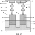
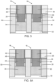
- a structure 10 for a resistive random-access memory device includes an array of bipolar junction transistors 12, 14, 16, 18 that may be fabricated using a silicon-on-insulator substrate that includes a semiconductor layer 28, a substrate 32, and a dielectric layer 30 disposed between the semiconductor layer 28 and the substrate 32.
- the semiconductor layer 28 may be comprised of a semiconductor material, such as single-crystal silicon, and may be lightly doped with a p-type dopant.
- the dielectric layer 30 may be comprised of a dielectric material, such as silicon dioxide, that is an electrical insulator.
- the substrate 32 may be comprised of a semiconductor material, such as silicon, and the substrate 32 may be lightly doped with a p-type dopant.
- the dielectric layer 30 has an upper interface 13 with the semiconductor layer 28, the dielectric layer 30 has a lower interface 15 with the substrate 32, and the upper and lower interfaces 13, 15 may be separated by the thickness of the dielectric layer 30.
- Field-effect transistors (not shown) may be fabricated by CMOS processes in a region of the silicon-on-insulator substrate different from the region including the bipolar junction transistors 12, 14, 16, 18.
- the semiconductor layer 28 may have a thickness suitable to fabricate fully-depleted silicon-on-insulator (FDSOI) field-effect transistors.
- FDSOI fully-depleted silicon-on-insulator
- the semiconductor layer 28 may have a thickness in a range of about 2 nanometers (nm) to about 20 nm.
- the dielectric layer 30 may have a thickness in a range of about 10 nm to about 50 nm.
- Wells 34, 36 may be formed as doped regions in the substrate 32 that are positioned in a vertical direction beneath the interface 15 between the dielectric layer 30 and the substrate 32.
- the wells 34, 36 may adjoin the interface 15 between the dielectric layer 30 and the substrate 32.
- the wells 34, 36 may longitudinally extend as stripes of doped semiconductor material, and the well 34 may be aligned parallel to the well 36.
- the semiconductor material constituting the wells 34, 36 may have an opposite conductivity type from the semiconductor material constituting the substrate 32.
- a portion of the substrate 32 is arranged in a lateral direction between the well 34 and the well 36, and the oppositely-doped portion of the substrate 32 may electrically isolate the well 34 from the well 36.
- the wells 34, 36 may be contacted at an edge of the transistor array.
- the wells 34, 36 may be formed in the substrate 32 by introducing a dopant by, for example, ion implantation with given implantation conditions.
- a patterned implantation mask may be formed to define selected areas that are exposed for the implantation of ions.
- the implantation mask may include a layer of an organic photoresist that is applied and patterned to form openings exposing the selected areas and determining, at least in part, the location and horizontal dimensions of the wells 34, 36.
- the implantation mask has a thickness and stopping power sufficient to block the implantation of ions in masked areas.
- the implantation conditions e.g., ion species, dose, kinetic energy
- the wells 34, 36 may be doped with a concentration of an n-type dopant (e.g., arsenic or phosphorus) such that the wells 34, 36 have n-type conductivity.
- an n-type dopant e.g., arsenic or phosphorus
- the bipolar junction transistor 12 includes a base layer 20 that adjoins an underlying portion of the well 34, and the adjoined portion of the well 34 may define a collector of the bipolar junction transistor 12.
- the bipolar junction transistor 14 includes a base layer 22 that adjoins an underlying portion of the well 34, and the adjoined portion of the well 34 may define a collector of the bipolar junction transistor 14.
- the base layer 20 is connected to the base layer 22 by a section of the semiconductor layer 28, and the base layers 20, 22 may be connected to adjacent base layers (not shown) by respective sections of the semiconductor layer 28 to define a base line 78 that may be contacted at an edge of the array.
- the bipolar junction transistor 16 includes a base layer 24 that adjoins an underlying portion of the well 36, and the adjoined portion of the well 36 may define a collector of the bipolar junction transistor 16.
- the bipolar junction transistor 18 includes a base layer 26 that adjoins an underlying portion of the well 36, and the adjoined portion of the well 36 may define a collector of the bipolar junction transistor 18.
- the base layer 24 is connected to the base layer 26 by a section of the semiconductor layer 28, and the base layers 24, 26 may be connected to adjacent base layers (not shown) by respective sections of the semiconductor layer 28 to define a base line 80 that may be contacted at an edge of the array.
- the base layers 20, 22 may define intrinsic bases of the bipolar junction transistors 12, 14 that adjoin the respective intersected portions of the well 34 along interfaces defining p-n junctions
- the base layers 24, 26 may define intrinsic bases of the bipolar junction transistors 16, 18 that adjoin the respective intersected portions of the well 36 along interfaces defining p-n junctions.
- the base layers 20, 22, 24, 26 may be formed by patterning trenches that penetrate through the semiconductor layer 28 and dielectric layer 30 with lithography and etching processes, depositing and planarizing a semiconductor layer to fill the trenches, and forming trench isolation regions 25 positioned between the base layer 20, 22 in one row and the base layers 24, 26 in an adjacent row.
- the base layers 20, 22, 24, 26 may be comprised of a semiconductor material that is doped to have an opposite conductivity type from the doped regions providing the wells 34, 36.
- the base layers 20, 22, 24, 26 may be comprised of silicon.
- the base layers 20, 22, 24, 26 may be comprised of silicon-germanium.
- the base layers 20, 22, 24, 26 may be comprised of silicon-germanium containing a germanium content of less than or equal to than 35 atomic percent and the balance silicon.
- the base layers 20, 22, 24, 26 may be doped with a concentration a p-type dopant (e.g., boron) such that the base layers 20, 22, 24, 26 have p-type conductivity.
- a p-type dopant e.g., boron
- the base layers 20, 22 extend through the semiconductor layer 28 and the dielectric layer 30 to adjoin the well 34, and the base layers 24, 26 extend through the semiconductor layer 28 and the dielectric layer 30 to adjoin the well 36.
- the base layers 20, 22, 24, 26 may extend in a vertical direction fully through the dielectric layer 30 from the level of the interface 13 to the level of the interface 15.
- lower portions of the base layers 20, 22, 24, 26 may be coplanar or substantially coplanar with the interface 15.
- the wells 34, 36 may be longitudinally aligned orthogonal to the base line 78 including the base layer 20, the base layer 24, and the sections of the semiconductor layer 28 connected to the base layers 20, 24. As best shown in FIG.
- the wells 34, 36 may be longitudinally aligned orthogonal to the base line 80 including the base layer 22, the base layer 26, and the sections of the semiconductor layer 28 connected to the base layers 22, 26.
- the sections of the semiconductor layer 28 in the base lines 78, 80 may be doped to have the same conductivity type (e.g., p-type) as the base layers 20, 22, 24, 26, 28, and the sections of the semiconductor layer 28 in the base lines 78, 80 are isolated from the substrate 32 by the dielectric layer 30.
- the trench isolation regions 25 electrically isolate the base layers 20, 24 in the base line 78 from the base layers 22, 26 in the base line 80.
- the trench isolation regions 25 may be formed by patterning shallow trenches with lithography and etching processes, depositing a dielectric material, such as silicon dioxide, to fill the shallow trenches, and planarizing and/or recessing the dielectric material.
- One of the trench isolation regions 25 is positioned between the base layer 20 and the base layer 22, and another of the trench isolation regions 25 is positioned between the base layer 24 and the base layer 26.
- Alignment structures 38 are formed that may be aligned parallel to each other and that may extend parallel to the wells 34, 36.
- the alignment structures 38 may be dummy gate structures formed by a CMOS process and that may include a layer of polysilicon stacked on a layer of a dielectric material, such as silicon dioxide.
- the alignment structures 38 are positioned on the semiconductor layer 28 and, in particular, on the sections of the semiconductor layer 28 participating in the base lines 78, 80.
- the alignment structures 38 may be electrically non-functional in the bipolar junction transistors 12, 14, 16, 18.
- the bipolar junction transistor 12 includes an emitter 40 that adjoins the base layer 20 along an interface defining a p-n junction.
- the bipolar junction transistor 14 includes an emitter 42 that adjoins the base layer 22 along an interface defining a p-n junction.
- the bipolar junction transistor 16 includes an emitter 44 that adjoins the base layer 24 along an interface defining a p-n junction.
- the bipolar junction transistor 18 includes an emitter 46 that adjoins the base layer 26 along an interface defining a p-n junction.
- One of the trench isolation regions 25 is positioned in a lateral direction between the emitter 40 and the emitter 42, and one of the trench isolation regions 25 is positioned in a lateral direction between the emitter 44 and the emitter 46.
- the emitters 40, 42, 44, 46 may be respectively formed as raised semiconductor layers on the base layers 20, 22, 24, 26 at the intersections between the base lines 78, 80 and the wells 34, 36.
- the base layers 20, 22, 24, 26 are positioned in a vertical direction between the portions of the wells 34, 36 defining the collectors and the emitters 40, 42, 44, 46.
- the emitters 40, 42, 44, 46 may be formed by epitaxially growing semiconductor material.
- the alignment structures 38 and the trench isolation regions 25 may function to self-align the formation of the emitters 40, 42, 44, 46 in a selective epitaxial growth process.
- the respective surface areas of the base layers 20, 22, 24, 26 contacted by the emitters 40, 42, 44, 46 are constrained by the alignment structures 38 and the trench isolation regions 25 such that the cross-sectional areas of the emitters 40, 42, 44, 46 in a vertical perspective are equal to the contacted surface areas of the base layers 20, 22, 24, 26.
- the semiconductor material of the emitters 40, 42, 44, 46 may be doped to have the same conductivity type as the wells 34, 36 and an opposite conductivity type from the base layers 20, 22, 24, 26.
- the semiconductor material of the emitters 40, 42, 44, 46 may be doped (e.g., heavily doped) with a concentration of an n-type dopant (e.g., arsenic or phosphorus) such that the emitters 40, 42, 44, 46 have n-type conductivity.
- an n-type dopant e.g., arsenic or phosphorus
- Spacers 48 may be positioned between the alignment structures 38 and the emitters 40, 42, 44, 46.
- the spacers 48 may be formed on the alignment structures 38, before forming the emitters 40, 42, 44, 46, by depositing a layer comprised of a dielectric material, such as silicon nitride, that is an electrical insulator and etching the deposited layer with an anisotropic etching process.
- a dielectric material such as silicon nitride
- the structure 10 may be formed in a BiCMOS process with a minimal number of added masks.
- the formation of the emitters 40, 42, 44, 46 may be shared with the formation of raised sources and drains of field-effect transistors formed on the same chip as the bipolar junction transistors 12, 14, 16, 18.
- the bipolar junction transistors 12, 14, 16, 18, which have a vertical arrangement of p-n junctions, can be formed with a more compact size than field-effect transistors, which may permit downward scaling in the dimensions of an associated resistive random-access memory device due to the elimination of field-effect transistors as access transistors.
- an interconnect structure may be formed over the bipolar junction transistors 12, 14, 16, 18.
- the interconnect structure may include dielectric layers 60, 62, 64 arranged in a layer stack defining multiple metallization levels.
- the dielectric layers 60, 62, 64 may be comprised of a dielectric material, such as silicon dioxide or a low-k dielectric material, that is an electrical insulator.
- Resistive memory elements 52, 54, 56, 58 may be formed as representative non-volatile memory elements in the interconnect structure.
- the resistive memory elements 52, 54, 56, 58 are respectively coupled to the bipolar junction transistors 12, 14, 16, 18 to define different bitcells of the resistive random-access memory device, and the bipolar junction transistors 12, 14, 16, 18 provide access transistors for accessing the bitcells.
- the well 34 may define a word line of the resistive random-access memory device for accessing the bipolar junction transistors 12, 14, and the well 36 may define another word line of the resistive random-access memory device for accessing the bipolar junction transistors 16, 18.
- the wells 34, 36 may be connected by a bus to peripheral circuits that include, for example, word line drivers.
- the base lines 78, 80 may define bit lines of the resistive random-access memory device.
- the base lines 78, 80 may be connected by a bus to peripheral circuits that include, for example, bit line drivers, a multiplexer, and a sense amplifier.
- the bit lines defined by the base lines 78, 80 may be aligned orthogonal to the word lines defined by the wells 34, 36, which enables connections to be established to the bipolar junction transistors 12, 14, 16, 18 at edges of the array for reading, writing, and erasing the resistive memory elements 52, 54, 56, 58.
- the resistive memory elements 52, 54, 56, 58 may arranged in an array that is characterized by rows and columns and that may be spatially coordinated with the array of bipolar junction transistors 12, 14, 16, 18.
- Each of the resistive memory elements 52, 54, 56, 58 includes a bottom electrode 68, a top electrode 72, and a switching layer 70 positioned between the bottom electrode 68 and the top electrode 72.
- the bottom electrodes 68 may define respective cathodes of the resistive memory elements 52, 54, 56, 58, and the top electrodes 72 may define respective anodes of the resistive memory elements 52, 54, 56, 58.
- Each bottom electrode 68 comprised of a metal, such as tantalum, titanium nitride, tantalum nitride, or a combination thereof.
- Each switching layer 70 may be comprised of a metal oxide, such as hafnium oxide, magnesium oxide, tantalum oxide, titanium oxide, or aluminum oxide, or a dielectric material, such as silicon nitride or silicon dioxide.
- Each top electrode 72 may be comprised of a metal, such as tungsten, titanium nitride, tantalum nitride, or platinum.
- the interconnect structure may include vertical interconnections 76 defined by a stack of contacts, via plugs, and metal features that physically and electrically connect the emitter 40 of the bipolar junction transistor 12 to the bottom electrode 68 of the resistive memory element 52, the emitter 42 of the bipolar junction transistor 14 to the bottom electrode 68 of the resistive memory element 54, the emitter 44 of the bipolar junction transistor 16 to the bottom electrode 68 of the resistive memory element 56, and the emitter 46 of the bipolar junction transistor 18 to the bottom electrode 68 of the resistive memory element 58.
- the structure 10 for the resistive random-access memory device may be expanded to include additional bipolar junction transistors and additional resistive memory elements.
- the expanded array may include additional wells arranged adjacent to the wells 34, 36, additional base lines arranged adjacent to the base lines 78, 80, and additional emitters at the intersections of the additional base lines and additional wells.
- the number of resistive memory elements in the expanded array may be increased commensurate with the increased number of bipolar junction transistors.
- the resistive memory elements 52, 54, 56, 58 may be replaced by a different non-volatile memory elements, such as magnetoresistive memory elements.
- trench isolation regions 50 may be formed in the spaces between the wells 34, 36.
- the trench isolation regions 50 may extend to a greater depth in the substrate 32 than the wells 34, 36.
- the trench isolation regions 50 which are comprised of a dielectric material, such as silicon dioxide, may be formed along with the trench isolation regions 25.
- One of the trench isolation regions 50 is positioned in a lateral direction between the well 34 and the well 36 to electrically isolate the well 34 from the well 36.
- the methods as described above are used in the fabrication of integrated circuit chips.
- the resulting integrated circuit chips can be distributed by the fabricator in raw wafer form (e.g., as a single wafer that has multiple unpackaged chips), as a bare die, or in a packaged form.
- the chip may be integrated with other chips, discrete circuit elements, and/or other signal processing devices as part of either an intermediate product or an end product.
- the end product can be any product that includes integrated circuit chips, such as computer products having a central processor or smartphones.
- references herein to terms modified by language of approximation, such as “about”, “approximately”, and “substantially”, are not to be limited to the precise value specified.
- the language of approximation may correspond to the precision of an instrument used to measure the value and, unless otherwise dependent on the precision of the instrument, may indicate a range of +/- 10% of the stated value(s).
- references herein to terms such as “vertical”, “horizontal”, etc. are made by way of example, and not by way of limitation, to establish a frame of reference.
- the term “horizontal” as used herein is defined as a plane parallel to a conventional plane of a semiconductor substrate, regardless of its actual three-dimensional spatial orientation.
- the terms “vertical” and “normal” refer to a direction in the frame of reference perpendicular to the horizontal, as just defined.
- the term “lateral” refers to a direction in the frame of reference within the horizontal plane.
- a feature “connected” or “coupled” to or with another feature may be directly connected or coupled to or with the other feature or, instead, one or more intervening features may be present.
- a feature may be “directly connected” or “directly coupled” to or with another feature if intervening features are absent.
- a feature may be “indirectly connected” or “indirectly coupled” to or with another feature if at least one intervening feature is present.
- a feature “on” or “contacting” another feature may be directly on or in direct contact with the other feature or, instead, one or more intervening features may be present.
- a feature may be “directly on” or in “direct contact” with another feature if intervening features are absent.
- a feature may be “indirectly on” or in “indirect contact” with another feature if at least one intervening feature is present.
- Different features may “overlap” if a feature extends over, and covers a part of, another feature.
Landscapes
- Metal-Oxide And Bipolar Metal-Oxide Semiconductor Integrated Circuits (AREA)
- Bipolar Transistors (AREA)
Claims (15)
- Struktur umfassend:eine Halbleiterschicht (28) umfassend eine erste Sektion;ein Substrat (32);eine zwischen der Halbleiterschicht (28) und dem Substrat (32) angeordnete dielektrische Schicht (30); undeinen ersten Bipolartransistor (12) umfassend einen ersten Kollektor in dem Substrat (32), einen ersten Emitter (40), und eine zwischen dem ersten Kollektor und dem ersten Emitter (40) positionierte erste Basisschicht (20), wobei sich die erste Basisschicht (20) durch die dielektrische Schicht (30) von dem ersten Emitter (40) zu dem ersten Kollektor erstreckt; undeinen zweiten Bipolartransistor (16) umfassend einen zweiten Kollektor in dem Substrat (32), einen zweiten Emitter (44), und eine zwischen dem zweiten Kollektor und dem zweiten Emitter (44) positionierte zweite Basisschicht (24), wobei sich die zweite Basisschicht (24) durch die dielektrische Schicht (30) von dem zweiten Emitter (44) zu dem zweiten Kollektor erstreckt, und die zweite Basisschicht (24) mit der ersten Basisschicht (20) durch die erste Sektion der Halbleiterschicht (28) verbunden ist, um eine erste Basisleitung (78) zu definieren,wobei der erste Kollektor ein Abschnitt einer ersten Wanne (34) in dem Substrat (32) ist, und der zweite Kollektor ein Abschnitt einer zweiten Wanne (36) in dem Substrat (32) ist.
- Struktur nach Anspruch 1, wobei die erste Wanne (34) von der zweiten Wanne (36) durch einen Abschnitt des Substrats (32) getrennt ist.
- Struktur nach Anspruch 2, wobei die erste Wanne (34) und die zweite Wanne (36) eine n-Typ-Leitfähigkeit aufweisen, und der Abschnitt des Substrats (32) eine p-Typ-Leitfähigkeit aufweist.
- Struktur nach einem der Ansprüche 1 bis 3, ferner umfassend:
eine Grabenisolationsregion (50), die sich durch die Halbleiterschicht (32) und die dielektrische Schicht (30) in das Substrat (32) erstreckt, wobei die Grabenisolationsregion (50) zwischen der ersten Wanne (34) und der zweiten Wanne (36) positioniert ist. - Struktur nach einem der Ansprüche 1 bis 4, ferner umfassend:einen dritten Bipolartransistor (14) umfassend einen dritten Kollektor in dem Substrat (32), einen dritten Emitter (42), und eine dritte Basisschicht (22), wobei sich die dritte Basisschicht (22) durch die dielektrische Schicht (30) von dem dritten Emitter (42) zu dem dritten Kollektor erstreckt; undeine zwischen der ersten Basisschicht (20) und der dritten Basisschicht (22) positionierte Grabenisolationsregion (25).
- Struktur nach Anspruch 5, wobei sich die Grabenisolationsregion (25) in die erste Wanne (34) erstreckt, und/oder wobei die Grabenisolationsregion (25) in einer lateralen Richtung zwischen dem ersten Emitter (40) und dem dritten Emitter (42) positioniert ist.
- Struktur nach einem der Ansprüche 1 bis 6, wobei die erste Wanne (34) und die zweite Wanne (36) orthogonal zu der ersten Basisleitung (78) längs ausgerichtet ist.
- Struktur nach einem der Ansprüche 1 bis 7, ferner umfassend:
eine zwischen dem ersten Emitter (40) und dem zweiten Emitter (44) positionierte Ausrichtungsstruktur (38). - Struktur nach Anspruch 8, wobei die Ausrichtungsstruktur (38) eine Dummy-Gate-Struktur ist und/oder wobei die Ausrichtungsstruktur (38) an der ersten Sektion der Halbleiterschicht (28) positioniert ist.
- Struktur nach einem der Ansprüche 1 bis 9, ferner umfassend:ein mit dem ersten Emitter (40) des ersten Bipolartransistors (12) verbundenes erstes Speicherelement (52); undein mit dem zweiten Emitter (44) des zweiten Bipolartransistors (16) verbundenes zweites Speicherelement (56), wobei optional das erste Speicherelement (52) und das zweite Speicherelement (56) jeweils eine erste Elektrode (72), eine zweite Elektrode (68), und eine zwischen der ersten Elektrode (72) und der zweiten Elektrode (68) positionierte Schaltschicht (70) umfassen.
- Struktur nach Anspruch 10, ferner umfassend eine Interconnect-Struktur über dem ersten Bipolartransistor (12) und dem zweiten Bipolartransistor (16), wobei die Interconnect-Struktur eine Vielzahl von dielektrischen Schichten (60, 62, 64) in einem Schichtstapel umfasst, wobei das erste Speicherelement (52) und das zweite Speicherelement (56) in der Interconnect-Struktur positioniert sind.
- Struktur nach einem der Ansprüche 1 bis 11, wobei die Halbleiterschicht (28) eine zweite Sektion umfasst, und ferner umfassend:einen angrenzend an den ersten Bipolartransistor (12) positionierten dritten Bipolartransistor (14), wobei der dritte Bipolartransistor (14) einen dritten Kollektor in dem Substrat (32), einen dritten Emitter (42), und eine dritte Basisschicht (22) umfasst, wobei sich die dritte Basisschicht (22) durch die dielektrische Schicht (30) von dem dritten Emitter (42) zu dem dritten Kollektor erstreckt; undeinen vierten Bipolartransistor (18) umfassend einen vierten Kollektor in dem Substrat (32), einen vierten Emitter (46), und eine zwischen dem vierten Kollektor und dem vierten Emitter (46) positionierte vierte Basisschicht (26), wobei sich die vierte Basisschicht (26) durch die dielektrische Schicht (30) von dem vierten Emitter (46) zu dem vierten Kollektor erstreckt, und die vierte Basisschicht (26) mit der dritten Basisschicht (22) durch die zweite Sektion der Halbleiterschicht (28) verbunden ist, um eine zweite Basisleitung (80) zu definieren,wobei der erste Kollektor und der dritte Kollektor Abschnitte der ersten Wanne (34) sind, und der zweite Kollektor und der vierte Kollektor Abschnitte der zweiten Wanne (36) sind.
- Struktur nach Anspruch 12, ferner umfassend eine zwischen der ersten Basisleitung (78) und der zweiten Basisleitung (80) positionierte Grabenisolationsregion.
- Struktur nach einem der Ansprüche 1 bis 13, wobei der erste Kollektor, der erste Emitter (40), der zweite Kollektor, und der zweite Emitter (44) eine n-Typ-Leitfähigkeit aufweisen, und die erste Basisschicht (20) und die zweite Basisschicht (24) eine p-Typ-Leitfähigkeit aufweisen.
- Verfahren umfassend:Bilden eines ersten Bipolartransistors (12) umfassend einen ersten Kollektor in einem Substrat (32), einen ersten Emitter (40), und eine zwischen dem ersten Kollektor und dem ersten Emitter (40) positionierte erste Basisschicht (20), wobei eine dielektrische Schicht (30) zwischen einer Halbleiterschicht (28) und dem Substrat (32) angeordnet ist, und sich die erste Basisschicht (20) durch die dielektrische Schicht (30) von dem ersten Emitter (40) zu dem ersten Kollektor erstreckt; undBilden eines zweiten Bipolartransistors (16) umfassend einen zweiten Kollektor in dem Substrat (32), einen zweiten Emitter (44), und eine zwischen dem zweiten Kollektor und dem zweiten Emitter (44) positionierte zweite Basisschicht (24), wobei sich die zweite Basisschicht (24) durch die dielektrische Schicht (30) von dem zweiten Emitter (44) zu dem zweiten Kollektor erstreckt, und die zweite Basisschicht (24) mit der ersten Basisschicht (20) durch eine Sektion der Halbleiterschicht (28) verbunden ist, um eine Basisleitung (78) zu definieren,wobei der erste Kollektor ein Abschnitt einer ersten Wanne (34) in dem Substrat (32) ist, und der zweite Kollektor ein Abschnitt einer zweiten Wanne (36) in dem Substrat (32) ist.
Applications Claiming Priority (1)
| Application Number | Priority Date | Filing Date | Title |
|---|---|---|---|
| US17/990,898 US12464745B2 (en) | 2022-11-21 | 2022-11-21 | Bipolar junction transistor arrays |
Publications (3)
| Publication Number | Publication Date |
|---|---|
| EP4373237A1 EP4373237A1 (de) | 2024-05-22 |
| EP4373237C0 EP4373237C0 (de) | 2025-05-14 |
| EP4373237B1 true EP4373237B1 (de) | 2025-05-14 |
Family
ID=88097755
Family Applications (1)
| Application Number | Title | Priority Date | Filing Date |
|---|---|---|---|
| EP23198101.0A Active EP4373237B1 (de) | 2022-11-21 | 2023-09-19 | Bipolartransistorarrays |
Country Status (3)
| Country | Link |
|---|---|
| US (1) | US12464745B2 (de) |
| EP (1) | EP4373237B1 (de) |
| CN (1) | CN118448413A (de) |
Families Citing this family (2)
| Publication number | Priority date | Publication date | Assignee | Title |
|---|---|---|---|---|
| US12471294B2 (en) * | 2022-11-21 | 2025-11-11 | Globalfoundries U.S. Inc. | Array arrangements of vertical bipolar junction transistors |
| US12464745B2 (en) | 2022-11-21 | 2025-11-04 | Globalfoundries U.S. Inc. | Bipolar junction transistor arrays |
Family Cites Families (24)
| Publication number | Priority date | Publication date | Assignee | Title |
|---|---|---|---|---|
| JP2005244145A (ja) | 2004-01-28 | 2005-09-08 | Sharp Corp | 半導体記憶装置及びその製造方法 |
| JP4783070B2 (ja) | 2005-06-24 | 2011-09-28 | シャープ株式会社 | 半導体記憶装置及びその製造方法 |
| KR101481401B1 (ko) | 2008-05-19 | 2015-01-14 | 삼성전자주식회사 | 비휘발성 기억 장치 |
| US8476686B2 (en) | 2008-07-09 | 2013-07-02 | Infineon Technologies Ag | Memory device and method for making same |
| US8687403B1 (en) * | 2010-06-10 | 2014-04-01 | Adesto Technologies Corporation | Circuits having programmable impedance elements |
| US8603885B2 (en) | 2011-01-04 | 2013-12-10 | International Business Machines Corporation | Flat response device structures for bipolar junction transistors |
| US20130277753A1 (en) * | 2012-04-20 | 2013-10-24 | International Business Machines Corporation | Bicmos devices on etsoi |
| US9153672B2 (en) | 2012-12-21 | 2015-10-06 | Taiwan Semiconductor Manufacturing Co., Ltd. | Vertical BJT for high density memory |
| US8975146B2 (en) | 2013-05-01 | 2015-03-10 | International Business Machines Corporation | Trench isolation structures and methods for bipolar junction transistors |
| US9231074B2 (en) | 2013-07-19 | 2016-01-05 | Globalfoundries Inc. | Bipolar junction transistors with an air gap in the shallow trench isolation |
| US9059196B2 (en) * | 2013-11-04 | 2015-06-16 | International Business Machines Corporation | Bipolar junction transistors with self-aligned terminals |
| US9496250B2 (en) | 2014-12-08 | 2016-11-15 | Globalfoundries Inc. | Tunable scaling of current gain in bipolar junction transistors |
| US9543403B2 (en) | 2015-01-21 | 2017-01-10 | Globalfoundries Inc. | Bipolar junction transistor with multiple emitter fingers |
| US9871076B2 (en) * | 2016-04-05 | 2018-01-16 | Globalfoundries Singapore Pte. Ltd. | Domain wall magnetic memory |
| US10115810B2 (en) | 2017-02-20 | 2018-10-30 | Globalfoundries Inc. | Heterojunction bipolar transistor with a thickened extrinsic base |
| US10670638B2 (en) | 2017-11-09 | 2020-06-02 | Texas Instruments Incorporated | Layout for reduced cross-talk in common terminal transistor |
| US10411109B2 (en) | 2018-01-02 | 2019-09-10 | International Business Machines Corporation | Bipolar junction transistor (BJT) for liquid flow biosensing applications without a reference electrode and large sensing area |
| KR20190133349A (ko) | 2018-05-23 | 2019-12-03 | 삼성전자주식회사 | Esd 보호를 위한 반도체 장치 |
| US10916642B2 (en) | 2019-04-18 | 2021-02-09 | Globalfoundries U.S. Inc. | Heterojunction bipolar transistor with emitter base junction oxide interface |
| US11018188B2 (en) * | 2019-06-03 | 2021-05-25 | International Business Machines Corporation | Three-dimensional stackable multi-layer cross-point memory with bipolar junction transistor selectors |
| US12408417B2 (en) | 2022-02-28 | 2025-09-02 | Globalfoundries U.S. Inc. | Forksheet semiconductor structure including at least one bipolar junction transistor and method |
| TWI888717B (zh) | 2022-04-06 | 2025-07-01 | 聯華電子股份有限公司 | 靜電放電保護結構 |
| US12426278B2 (en) | 2022-10-26 | 2025-09-23 | Globalfoundries U.S. Inc. | Resistive memory elements accessed by bipolar junction transistors |
| US12464745B2 (en) | 2022-11-21 | 2025-11-04 | Globalfoundries U.S. Inc. | Bipolar junction transistor arrays |
-
2022
- 2022-11-21 US US17/990,898 patent/US12464745B2/en active Active
-
2023
- 2023-09-19 EP EP23198101.0A patent/EP4373237B1/de active Active
- 2023-10-20 CN CN202311368471.3A patent/CN118448413A/zh active Pending
Also Published As
| Publication number | Publication date |
|---|---|
| US20240170560A1 (en) | 2024-05-23 |
| CN118448413A (zh) | 2024-08-06 |
| US12464745B2 (en) | 2025-11-04 |
| EP4373237C0 (de) | 2025-05-14 |
| EP4373237A1 (de) | 2024-05-22 |
Similar Documents
| Publication | Publication Date | Title |
|---|---|---|
| US6246083B1 (en) | Vertical gain cell and array for a dynamic random access memory | |
| JP4044293B2 (ja) | 半導体装置及びその製造方法 | |
| JP3322936B2 (ja) | 半導体記憶装置 | |
| US6528837B2 (en) | Circuit and method for an open bit line memory cell with a vertical transistor and trench plate trench capacitor | |
| US8686494B2 (en) | Recessed channel negative differential resistance-based memory cell | |
| EP4373237B1 (de) | Bipolartransistorarrays | |
| CN113035867B (zh) | 存储器件和半导体器件 | |
| US12426278B2 (en) | Resistive memory elements accessed by bipolar junction transistors | |
| JPH10507592A (ja) | 縦型mosトランジスタを有する固定記憶装置の製造方法 | |
| EP4387410B1 (de) | Transistoranordnungen mit steuerbarer gate-spannung | |
| EP4312479B1 (de) | Resistive speicherelementarrays mit gemeinsam genutzten elektrodenstreifen und ein verfahren | |
| US12471294B2 (en) | Array arrangements of vertical bipolar junction transistors | |
| CN117855271A (zh) | 具有混合阱的铁电场效应晶体管 | |
| KR100911194B1 (ko) | 상변화 메모리 소자 및 그 제조방법 | |
| WO2024055422A1 (zh) | 半导体结构及其形成方法、半导体结构的操作方法 | |
| JP4565380B2 (ja) | 読み出し専用記憶装置 | |
| US20250159905A1 (en) | Switching memory elements accessed by heterojunction bipolar transistors | |
| KR100717279B1 (ko) | 마스크롬 소자 및 그 형성 방법 | |
| KR20240155822A (ko) | 반도체 메모리 장치 및 이의 제조 방법 |
Legal Events
| Date | Code | Title | Description |
|---|---|---|---|
| PUAI | Public reference made under article 153(3) epc to a published international application that has entered the european phase |
Free format text: ORIGINAL CODE: 0009012 |
|
| STAA | Information on the status of an ep patent application or granted ep patent |
Free format text: STATUS: THE APPLICATION HAS BEEN PUBLISHED |
|
| AK | Designated contracting states |
Kind code of ref document: A1 Designated state(s): AL AT BE BG CH CY CZ DE DK EE ES FI FR GB GR HR HU IE IS IT LI LT LU LV MC ME MK MT NL NO PL PT RO RS SE SI SK SM TR |
|
| STAA | Information on the status of an ep patent application or granted ep patent |
Free format text: STATUS: REQUEST FOR EXAMINATION WAS MADE |
|
| 17P | Request for examination filed |
Effective date: 20240905 |
|
| RBV | Designated contracting states (corrected) |
Designated state(s): AL AT BE BG CH CY CZ DE DK EE ES FI FR GB GR HR HU IE IS IT LI LT LU LV MC ME MK MT NL NO PL PT RO RS SE SI SK SM TR |
|
| RIC1 | Information provided on ipc code assigned before grant |
Ipc: H10N 70/20 20230101ALN20250102BHEP Ipc: H10B 61/00 20230101ALN20250102BHEP Ipc: H10D 84/60 20250101ALI20250102BHEP Ipc: H10B 63/00 20230101AFI20250102BHEP |
|
| GRAP | Despatch of communication of intention to grant a patent |
Free format text: ORIGINAL CODE: EPIDOSNIGR1 |
|
| STAA | Information on the status of an ep patent application or granted ep patent |
Free format text: STATUS: GRANT OF PATENT IS INTENDED |
|
| INTG | Intention to grant announced |
Effective date: 20250207 |
|
| RIN1 | Information on inventor provided before grant (corrected) |
Inventor name: PRITCHARD, DAVID Inventor name: JAIN, VIBHOR Inventor name: YU, HONG Inventor name: PEKARIK, JOHN J. Inventor name: GOPINATH, VENKATESH Inventor name: DERRICKSON, ALEXANDER |
|
| GRAS | Grant fee paid |
Free format text: ORIGINAL CODE: EPIDOSNIGR3 |
|
| GRAA | (expected) grant |
Free format text: ORIGINAL CODE: 0009210 |
|
| STAA | Information on the status of an ep patent application or granted ep patent |
Free format text: STATUS: THE PATENT HAS BEEN GRANTED |
|
| AK | Designated contracting states |
Kind code of ref document: B1 Designated state(s): AL AT BE BG CH CY CZ DE DK EE ES FI FR GB GR HR HU IE IS IT LI LT LU LV MC ME MK MT NL NO PL PT RO RS SE SI SK SM TR |
|
| REG | Reference to a national code |
Ref country code: GB Ref legal event code: FG4D |
|
| REG | Reference to a national code |
Ref country code: CH Ref legal event code: EP |
|
| REG | Reference to a national code |
Ref country code: IE Ref legal event code: FG4D |
|
| U01 | Request for unitary effect filed |
Effective date: 20250514 |
|
| U07 | Unitary effect registered |
Designated state(s): AT BE BG DE DK EE FI FR IT LT LU LV MT NL PT RO SE SI Effective date: 20250520 |
|
| U20 | Renewal fee for the european patent with unitary effect paid |
Year of fee payment: 3 Effective date: 20250807 |
|
| PG25 | Lapsed in a contracting state [announced via postgrant information from national office to epo] |
Ref country code: ES Free format text: LAPSE BECAUSE OF FAILURE TO SUBMIT A TRANSLATION OF THE DESCRIPTION OR TO PAY THE FEE WITHIN THE PRESCRIBED TIME-LIMIT Effective date: 20250514 |
|
| PG25 | Lapsed in a contracting state [announced via postgrant information from national office to epo] |
Ref country code: NO Free format text: LAPSE BECAUSE OF FAILURE TO SUBMIT A TRANSLATION OF THE DESCRIPTION OR TO PAY THE FEE WITHIN THE PRESCRIBED TIME-LIMIT Effective date: 20250814 Ref country code: GR Free format text: LAPSE BECAUSE OF FAILURE TO SUBMIT A TRANSLATION OF THE DESCRIPTION OR TO PAY THE FEE WITHIN THE PRESCRIBED TIME-LIMIT Effective date: 20250815 |
|
| PG25 | Lapsed in a contracting state [announced via postgrant information from national office to epo] |
Ref country code: PL Free format text: LAPSE BECAUSE OF FAILURE TO SUBMIT A TRANSLATION OF THE DESCRIPTION OR TO PAY THE FEE WITHIN THE PRESCRIBED TIME-LIMIT Effective date: 20250514 |
|
| PG25 | Lapsed in a contracting state [announced via postgrant information from national office to epo] |
Ref country code: HR Free format text: LAPSE BECAUSE OF FAILURE TO SUBMIT A TRANSLATION OF THE DESCRIPTION OR TO PAY THE FEE WITHIN THE PRESCRIBED TIME-LIMIT Effective date: 20250514 |
|
| PG25 | Lapsed in a contracting state [announced via postgrant information from national office to epo] |
Ref country code: RS Free format text: LAPSE BECAUSE OF FAILURE TO SUBMIT A TRANSLATION OF THE DESCRIPTION OR TO PAY THE FEE WITHIN THE PRESCRIBED TIME-LIMIT Effective date: 20250814 |
|
| PG25 | Lapsed in a contracting state [announced via postgrant information from national office to epo] |
Ref country code: IS Free format text: LAPSE BECAUSE OF FAILURE TO SUBMIT A TRANSLATION OF THE DESCRIPTION OR TO PAY THE FEE WITHIN THE PRESCRIBED TIME-LIMIT Effective date: 20250914 |
|
| PG25 | Lapsed in a contracting state [announced via postgrant information from national office to epo] |
Ref country code: SM Free format text: LAPSE BECAUSE OF FAILURE TO SUBMIT A TRANSLATION OF THE DESCRIPTION OR TO PAY THE FEE WITHIN THE PRESCRIBED TIME-LIMIT Effective date: 20250514 |
|
| PG25 | Lapsed in a contracting state [announced via postgrant information from national office to epo] |
Ref country code: CZ Free format text: LAPSE BECAUSE OF FAILURE TO SUBMIT A TRANSLATION OF THE DESCRIPTION OR TO PAY THE FEE WITHIN THE PRESCRIBED TIME-LIMIT Effective date: 20250514 |
|
| PG25 | Lapsed in a contracting state [announced via postgrant information from national office to epo] |
Ref country code: SK Free format text: LAPSE BECAUSE OF FAILURE TO SUBMIT A TRANSLATION OF THE DESCRIPTION OR TO PAY THE FEE WITHIN THE PRESCRIBED TIME-LIMIT Effective date: 20250514 |
|
| PLBE | No opposition filed within time limit |
Free format text: ORIGINAL CODE: 0009261 |
|
| STAA | Information on the status of an ep patent application or granted ep patent |
Free format text: STATUS: NO OPPOSITION FILED WITHIN TIME LIMIT |
|
| REG | Reference to a national code |
Ref country code: CH Ref legal event code: L10 Free format text: ST27 STATUS EVENT CODE: U-0-0-L10-L00 (AS PROVIDED BY THE NATIONAL OFFICE) Effective date: 20260325 |