EP4369382A1 - Dmos device having junction field plate and manufacturing method therefor - Google Patents
Dmos device having junction field plate and manufacturing method therefor Download PDFInfo
- Publication number
- EP4369382A1 EP4369382A1 EP22914399.5A EP22914399A EP4369382A1 EP 4369382 A1 EP4369382 A1 EP 4369382A1 EP 22914399 A EP22914399 A EP 22914399A EP 4369382 A1 EP4369382 A1 EP 4369382A1
- Authority
- EP
- European Patent Office
- Prior art keywords
- trench
- polycrystalline silicon
- silicon layer
- doped
- doped polycrystalline
- Prior art date
- Legal status (The legal status is an assumption and is not a legal conclusion. Google has not performed a legal analysis and makes no representation as to the accuracy of the status listed.)
- Pending
Links
Images



Classifications
-
- H—ELECTRICITY
- H10—SEMICONDUCTOR DEVICES; ELECTRIC SOLID-STATE DEVICES NOT OTHERWISE PROVIDED FOR
- H10D—INORGANIC ELECTRIC SEMICONDUCTOR DEVICES
- H10D30/00—Field-effect transistors [FET]
- H10D30/01—Manufacture or treatment
- H10D30/021—Manufacture or treatment of FETs having insulated gates [IGFET]
-
- H—ELECTRICITY
- H10—SEMICONDUCTOR DEVICES; ELECTRIC SOLID-STATE DEVICES NOT OTHERWISE PROVIDED FOR
- H10D—INORGANIC ELECTRIC SEMICONDUCTOR DEVICES
- H10D30/00—Field-effect transistors [FET]
- H10D30/01—Manufacture or treatment
- H10D30/021—Manufacture or treatment of FETs having insulated gates [IGFET]
- H10D30/028—Manufacture or treatment of FETs having insulated gates [IGFET] of double-diffused metal oxide semiconductor [DMOS] FETs
- H10D30/0281—Manufacture or treatment of FETs having insulated gates [IGFET] of double-diffused metal oxide semiconductor [DMOS] FETs of lateral DMOS [LDMOS] FETs
- H10D30/0289—Manufacture or treatment of FETs having insulated gates [IGFET] of double-diffused metal oxide semiconductor [DMOS] FETs of lateral DMOS [LDMOS] FETs using recessing of the gate electrodes, e.g. to form trench gate electrodes
-
- H—ELECTRICITY
- H10—SEMICONDUCTOR DEVICES; ELECTRIC SOLID-STATE DEVICES NOT OTHERWISE PROVIDED FOR
- H10D—INORGANIC ELECTRIC SEMICONDUCTOR DEVICES
- H10D30/00—Field-effect transistors [FET]
- H10D30/01—Manufacture or treatment
- H10D30/021—Manufacture or treatment of FETs having insulated gates [IGFET]
- H10D30/028—Manufacture or treatment of FETs having insulated gates [IGFET] of double-diffused metal oxide semiconductor [DMOS] FETs
- H10D30/0291—Manufacture or treatment of FETs having insulated gates [IGFET] of double-diffused metal oxide semiconductor [DMOS] FETs of vertical DMOS [VDMOS] FETs
- H10D30/0297—Manufacture or treatment of FETs having insulated gates [IGFET] of double-diffused metal oxide semiconductor [DMOS] FETs of vertical DMOS [VDMOS] FETs using recessing of the gate electrodes, e.g. to form trench gate electrodes
-
- H—ELECTRICITY
- H10—SEMICONDUCTOR DEVICES; ELECTRIC SOLID-STATE DEVICES NOT OTHERWISE PROVIDED FOR
- H10D—INORGANIC ELECTRIC SEMICONDUCTOR DEVICES
- H10D30/00—Field-effect transistors [FET]
- H10D30/60—Insulated-gate field-effect transistors [IGFET]
-
- H—ELECTRICITY
- H10—SEMICONDUCTOR DEVICES; ELECTRIC SOLID-STATE DEVICES NOT OTHERWISE PROVIDED FOR
- H10D—INORGANIC ELECTRIC SEMICONDUCTOR DEVICES
- H10D30/00—Field-effect transistors [FET]
- H10D30/60—Insulated-gate field-effect transistors [IGFET]
- H10D30/64—Double-diffused metal-oxide semiconductor [DMOS] FETs
- H10D30/65—Lateral DMOS [LDMOS] FETs
- H10D30/658—Lateral DMOS [LDMOS] FETs having trench gate electrodes
-
- H—ELECTRICITY
- H10—SEMICONDUCTOR DEVICES; ELECTRIC SOLID-STATE DEVICES NOT OTHERWISE PROVIDED FOR
- H10D—INORGANIC ELECTRIC SEMICONDUCTOR DEVICES
- H10D30/00—Field-effect transistors [FET]
- H10D30/60—Insulated-gate field-effect transistors [IGFET]
- H10D30/64—Double-diffused metal-oxide semiconductor [DMOS] FETs
- H10D30/66—Vertical DMOS [VDMOS] FETs
- H10D30/664—Inverted VDMOS transistors, i.e. source-down VDMOS transistors
-
- H—ELECTRICITY
- H10—SEMICONDUCTOR DEVICES; ELECTRIC SOLID-STATE DEVICES NOT OTHERWISE PROVIDED FOR
- H10D—INORGANIC ELECTRIC SEMICONDUCTOR DEVICES
- H10D30/00—Field-effect transistors [FET]
- H10D30/60—Insulated-gate field-effect transistors [IGFET]
- H10D30/64—Double-diffused metal-oxide semiconductor [DMOS] FETs
- H10D30/66—Vertical DMOS [VDMOS] FETs
- H10D30/668—Vertical DMOS [VDMOS] FETs having trench gate electrodes, e.g. UMOS transistors
-
- H—ELECTRICITY
- H10—SEMICONDUCTOR DEVICES; ELECTRIC SOLID-STATE DEVICES NOT OTHERWISE PROVIDED FOR
- H10D—INORGANIC ELECTRIC SEMICONDUCTOR DEVICES
- H10D62/00—Semiconductor bodies, or regions thereof, of devices having potential barriers
- H10D62/10—Shapes, relative sizes or dispositions of the regions of the semiconductor bodies; Shapes of the semiconductor bodies
- H10D62/102—Constructional design considerations for preventing surface leakage or controlling electric field concentration
- H10D62/103—Constructional design considerations for preventing surface leakage or controlling electric field concentration for increasing or controlling the breakdown voltage of reverse-biased devices
- H10D62/105—Constructional design considerations for preventing surface leakage or controlling electric field concentration for increasing or controlling the breakdown voltage of reverse-biased devices by having particular doping profiles, shapes or arrangements of PN junctions; by having supplementary regions, e.g. junction termination extension [JTE]
- H10D62/106—Constructional design considerations for preventing surface leakage or controlling electric field concentration for increasing or controlling the breakdown voltage of reverse-biased devices by having particular doping profiles, shapes or arrangements of PN junctions; by having supplementary regions, e.g. junction termination extension [JTE] having supplementary regions doped oppositely to or in rectifying contact with regions of the semiconductor bodies, e.g. guard rings with PN or Schottky junctions
-
- H—ELECTRICITY
- H10—SEMICONDUCTOR DEVICES; ELECTRIC SOLID-STATE DEVICES NOT OTHERWISE PROVIDED FOR
- H10D—INORGANIC ELECTRIC SEMICONDUCTOR DEVICES
- H10D64/00—Electrodes of devices having potential barriers
- H10D64/111—Field plates
-
- H—ELECTRICITY
- H10—SEMICONDUCTOR DEVICES; ELECTRIC SOLID-STATE DEVICES NOT OTHERWISE PROVIDED FOR
- H10D—INORGANIC ELECTRIC SEMICONDUCTOR DEVICES
- H10D64/00—Electrodes of devices having potential barriers
- H10D64/111—Field plates
- H10D64/117—Recessed field plates, e.g. trench field plates or buried field plates
-
- H—ELECTRICITY
- H10—SEMICONDUCTOR DEVICES; ELECTRIC SOLID-STATE DEVICES NOT OTHERWISE PROVIDED FOR
- H10D—INORGANIC ELECTRIC SEMICONDUCTOR DEVICES
- H10D64/00—Electrodes of devices having potential barriers
- H10D64/20—Electrodes characterised by their shapes, relative sizes or dispositions
- H10D64/23—Electrodes carrying the current to be rectified, amplified, oscillated or switched, e.g. sources, drains, anodes or cathodes
- H10D64/251—Source or drain electrodes for field-effect devices
- H10D64/252—Source or drain electrodes for field-effect devices for vertical or pseudo-vertical devices
-
- H—ELECTRICITY
- H10—SEMICONDUCTOR DEVICES; ELECTRIC SOLID-STATE DEVICES NOT OTHERWISE PROVIDED FOR
- H10P—GENERIC PROCESSES OR APPARATUS FOR THE MANUFACTURE OR TREATMENT OF DEVICES COVERED BY CLASS H10
- H10P32/00—Diffusion of dopants within, into or out of wafers, substrates or parts of devices
- H10P32/10—Diffusion of dopants within, into or out of semiconductor bodies or layers
- H10P32/14—Diffusion of dopants within, into or out of semiconductor bodies or layers within a single semiconductor body or layer in a solid phase; between different semiconductor bodies or layers, both in a solid phase
-
- H—ELECTRICITY
- H10—SEMICONDUCTOR DEVICES; ELECTRIC SOLID-STATE DEVICES NOT OTHERWISE PROVIDED FOR
- H10P—GENERIC PROCESSES OR APPARATUS FOR THE MANUFACTURE OR TREATMENT OF DEVICES COVERED BY CLASS H10
- H10P32/00—Diffusion of dopants within, into or out of wafers, substrates or parts of devices
- H10P32/10—Diffusion of dopants within, into or out of semiconductor bodies or layers
- H10P32/17—Diffusion of dopants within, into or out of semiconductor bodies or layers characterised by the semiconductor material
- H10P32/171—Diffusion of dopants within, into or out of semiconductor bodies or layers characterised by the semiconductor material being group IV material
-
- H—ELECTRICITY
- H10—SEMICONDUCTOR DEVICES; ELECTRIC SOLID-STATE DEVICES NOT OTHERWISE PROVIDED FOR
- H10D—INORGANIC ELECTRIC SEMICONDUCTOR DEVICES
- H10D30/00—Field-effect transistors [FET]
- H10D30/60—Insulated-gate field-effect transistors [IGFET]
- H10D30/64—Double-diffused metal-oxide semiconductor [DMOS] FETs
- H10D30/66—Vertical DMOS [VDMOS] FETs
- H10D30/663—Vertical DMOS [VDMOS] FETs having both source contacts and drain contacts on the same surface, i.e. up-drain VDMOS
Definitions
- the present disclosure relates to the field of semiconductor device technologies, and in particular, to a DMOS device with a junction field plate and its manufacturing method.
- Double-diffused Metal-Oxide-Semiconductor (DMOS) devices are typical and widely applied high-voltage power semiconductor devices. By adding a lightly doped drift region between source and drain in a DMOS device, the majority of voltage falls in the lightly doped drift region, so that the voltage resistance capability of the device is improved and the device may be used as a power MOS device in an integrated circuit. According to different structures, the DMOS devices may be divided into two types: Lateral (horizontal) DMOS (LDMOS) devices and Vertical (longitudinal) DMOS (VDMOS) devices.
- LDMOS Lateral (horizontal) DMOS
- VDMOS Vertical (longitudinal) DMOS
- the LDMOS devices are Radio Frequency (RF) power devices with great market demand and broad development prospects.
- RF Radio Frequency
- silicon-based LDMOS devices are used in almost all base stations and long-range transmitters.
- the LDMOS devices are widely applied to RF amplifiers in High Frequency (HF), Very High Frequency (VHF), and Ultra High Frequency (UHF) communication systems, pulse radar, industrial, scientific and medical applications, avionics, and other fields. Since the LDMOS devices have advantages of high gain, high linearity, high voltage resistance, high output power, easy compatibility with a Complementary Metal Oxide Semiconductor (CMOS) technology, etc., the silicon-based LDMOS devices have become a new hotspot in RF semiconductor power devices.
- CMOS Complementary Metal Oxide Semiconductor
- BV Breakdown Voltage
- Rdson Specific on-Resistance
- the high BV may be achieved only by increasing a size of the drift region, which increases chip area and cost of the LDMOS device. More seriously, a relationship between Rdson and BV of the device may be expressed as Rdson ⁇ BV 2.5 . That is, increasing the size of the drift region will increase Rdson, which leads to a sharp increase in power consumption, followed by a decrease in device switching speed.
- a purpose of the present disclosure is to provide a DMOS device with a junction field plate and its manufacturing method, so as to solve the problem that DMOS devices cannot effectively improve voltage resistance or decrease Rdson in prior art.
- the present disclosure provides a method for manufacturing a DMOS device with a junction field plate.
- the method for manufacturing the DMOS device with the junction field plate includes:
- providing the semiconductor substrate, in which the first trench is formed includes: forming a second trench in communication with the first trench in the semiconductor substrate;
- the first conduction type is of a P-type, and the second conduction type is of an N-type; forming the first doped polycrystalline silicon layer with the first conduction type on the semiconductor substrate includes:
- the first conduction type is of a P-type
- the second conduction type is of an N-type
- performing the first doping process and the second doping process on the first doped polycrystalline silicon layer includes: doping phosphonium ions, with a doping concentration from 1E17 atom/cm -3 to 1E18 atom/cm -3 , in the first doping process; and doping indium ions, with a doping concentration from 1E20 atom/cm -3 to 1E21 atom/cm -3 , in the second doping process.
- performing the heat treatment process, so that the second doped polycrystalline silicon layer in the first trench extends toward the side surfaces of the first trench further includes: a diffusion speed of doping ions in the first doping process being faster than that in the second doping process, so that an extension length of the first doped sublayer in the first trench toward the side surfaces of the first trench is greater than that of the second doped sublayer in the first trench toward the side surfaces of the first trench, and an extension length of the first doped sublayer in the second trench toward the side surfaces of the second trench is greater than that of the second doped sublayer in the second trench toward the side surfaces of the second trench.
- performing the heat treatment process, so that the second doped polycrystalline silicon layer in the first trench extends toward the side surfaces of the first trench further includes: the second doped polycrystalline silicon layer on the surface of the semiconductor substrate covers a portion of the side surfaces of the first trench and a portion of the side surfaces of the second trench.
- removing the portion of the second doped polycrystalline silicon layer to expose the portion of the bottom surface of the first trench includes:
- the first conduction type is of a P-type
- the second conduction type is of an N-type
- forming the body region and the source region located in the body region at the bottom of the first trench includes:
- removing the first doped polycrystalline silicon layer on the side surfaces of the second trench, where the second doped polycrystalline silicon layer in the second trench serves as the gate lead-out layer, and the gate lead-out layer is connected to the gate electrode includes:
- the present disclosure further provides a DMOS device with a junction field plate.
- the DMOS device with the junction field plate includes:
- a second trench in communication with the first trench is further formed in the semiconductor substrate, the second doped polycrystalline silicon layer covers a bottom surface of the second trench, the second doped polycrystalline silicon layer in the second trench serves as a gate lead-out layer, the gate lead-out layer is connected to the gate electrode, and the third lead-out structure is connected to the gate lead-out layer to achieve electrical connection with the gate electrode.
- the second doped polycrystalline silicon layer, the first doped polycrystalline silicon layer, and the third doped sublayer are sequentially in adjacent contact and cover side surfaces of the first trench.
- the second doped sublayer is located in the first doped sublayer, and in the first trench, a bottom surface of the first doped polycrystalline silicon layer is connected to the first doped sublayer and the second doped sublayer.
- the second trench in a first direction, is in communication with the first trench; in a second direction, the second trench is separated from the first trench, where the first direction is perpendicular to the second direction.
- the body region surrounds the bottom of the first trench.
- a drain region is located on a surface of a semiconductor substrate.
- a source region is located in the semiconductor substrate at a bottom of a first trench.
- a gate electrode is located at the bottom of the first trench. Therefore, lateral voltage resistance relative to LDMOS is changed to longitudinal voltage resistance, which may reduce a size of the entire device, decrease Rdson, and greatly optimize a contradiction relationship between voltage resistance and Rdson. Further, a junction field plate structure is formed in the DMOS device, which improves an effect on reducing surface resistance (Resurf).
- a depth of trenches in the DMOS device may be reduced, and thereby a depth-to-width ratio of the device is reduced, improving the feasibility of increasing a voltage resistance level.
- both the source region and the drain region in the DMOS device are led out on a same surface, which may be compatible with a technology for manufacturing a CMOS device.
- a second doped polycrystalline silicon layer includes a first doped sublayer and a second doped sublayer located on the first doped sublayer.
- the first doped sublayer and the second doped sublayer are of different conduction types. Therefore, in a case of an N-type gate electrode, a P-type doped layer may be directly connected to a potential of the gate electrode, which improves an effect of the junction field plate.
- first”, “second”, etc. serve only to distinguish structures/steps from each other, but do not indicate a sequential relationship between these structures/steps.
- a core idea of the present disclosure is to provide a DMOS device with a junction field plate and its manufacturing method.
- a drain region is located on a surface of a semiconductor substrate.
- a source region is located in the semiconductor substrate at a bottom of a first trench.
- a gate electrode is located at the bottom of the first trench. Therefore, lateral voltage resistance relative to LDMOS is changed to longitudinal voltage resistance, which may reduce a size of the entire device, decrease Rdson, and greatly optimize a contradiction relationship between voltage resistance and Rdson.
- a junction field plate structure is formed in the DMOS device, which improves an effect on reducing surface resistance (Resurf).
- a depth of trenches in the DMOS device may be reduced, and thereby a depth-to-width ratio of the device is reduced, improving the feasibility of increasing a voltage resistance level.
- both the source region and the drain region in the DMOS device are led out on a same surface, which may be compatible with a technology for manufacturing a CMOS device.
- a second doped polycrystalline silicon layer includes a first doped sublayer and a second doped sublayer located on the first doped sublayer.
- the first doped sublayer and the second doped sublayer are of different conduction types. Therefore, in a case of an N-type gate electrode, a P-type doped layer may be directly connected to a potential of the gate electrode, which improves an effect of the junction field plate.
- the DMOS device may be either an N-type DMOS device or a P-type DMOS device.
- the N-type DMOS device is taken as an example for detailed description. Based on the detailed description of the N-type DMOS device, those skilled in the art may obtain the P-type DMOS device and its manufacturing method accordingly, which will not be repeated here.
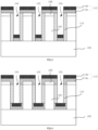
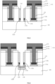
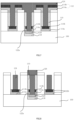
- FIGs. 1 to 12 are structural schematic diagrams illustrating components formed in executing a method for manufacturing a DMOS device with a junction field plate according to an embodiment of the present disclosure.
- a semiconductor substrate 100 is provided, and a first trench 102 and a second trench 104 are formed in the semiconductor substrate 100.
- the semiconductor substrate 100 is provided, and then a doping process is performed on the semiconductor substrate 100 to form a drift region 106 in the semiconductor substrate 100, where the drift region 106 may be formed by using any one known technology.
- a first hard mask layer 108 is formed on a surface of the semiconductor substrate 100, and the first hard mask layer 108 may be specifically of a multi-layer structure.
- the first hard mask layer 108 may be of a multi-layer structure with three layers of ONO (oxide-SIN-oxide).
- the first hard mask layer 108 undergoes a patterning process to expose a portion of the surface of the semiconductor substrate 100. Subsequently, an etching process may be performed on the exposed semiconductor substrate 100 to form the first trench 102 and the second trench 104.
- the first trench 102 and the second trench 104 are respectively located on two sides of the drift region 106. That is, the drift region 106 is formed in the semiconductor substrate 100 between the first trench 102 and the second trench 104.
- a first dielectric layer (not shown in FIG. 1 ) is formed on the semiconductor substrate 100, and the first dielectric layer covers surfaces of the semiconductor substrate 100, the first trench 102, and the second trench 104.
- the first dielectric layer may be specifically an oxide layer, a nitride layer, or the like.
- a first doped polycrystalline silicon layer 110 is formed on the semiconductor substrate 100, and the first doped polycrystalline silicon layer 110 covers the surface of the semiconductor substrate 100, the surface of the first trench 102, and the surface of the second trench 104. Specifically, in the embodiments of the present application, the first doped polycrystalline silicon layer 110 covers an upper surface of the first hard mask layer 108, side surfaces and a bottom surface of the first trench 102, and side surfaces and a bottom surface of the second trench 104. In the embodiments of the present application, the first doped polycrystalline silicon layer 110 covers the first dielectric layer.
- a thickness of the first doped polycrystalline silicon layer 110 is from 0.15 ⁇ m to 0.35 ⁇ m.
- the thickness of the first doped polycrystalline silicon layer 110 may be 0.18 ⁇ m, 0.20 ⁇ m, 0.25 ⁇ m, 0.27 ⁇ m or 0.33 ⁇ m.
- the first doped polycrystalline silicon layer 110 may be specifically formed in the following manners: forming a polycrystalline silicon layer (not shown in FIG. 2 ) on the semiconductor substrate 100, and performing a P-type doping process on the polycrystalline silicon layer to form the first doped polycrystalline silicon layer 110.
- a doping concentration for the first doped polycrystalline silicon layer is from 4E14 atom/cm -3 to 1E16 atom/cm -3 .
- the doping concentration for the first doped polycrystalline silicon layer may be 8E14 atom/cm -3 , 1E15 atom/cm -3 , 5E15 atom/cm -3 or 9E15 atom/cm -3 .
- Doping ions may be, for example, boron (B).
- an N-type doping process and a P-type doping process are performed on the first doped polycrystalline silicon layer 110 to form a second doped polycrystalline silicon layer 112 on the surface of the semiconductor substrate 100, a portion of the bottom surface of the first trench 102, and a portion of the bottom surface of the second trench 104.
- the second doped polycrystalline silicon layer 112 includes a first doped sublayer 114a and a second doped sublayer 114b located on the first doped sublayer 114a.
- the first doped sublayer 114a is of an N-type
- the second doped sublayer 114b is of a P-type.
- the second doped sublayer 114b is heavily doped. That is, the first doped polycrystalline silicon layer 110 is a lightly doped P-type conduction layer, and the second doped sublayer 114b is a heavily doped P-type conduction layer.
- a doping process may be performed on the entire semiconductor substrate 100 by using a universal injection technology, which may reduce process cost.
- N-type doping ions are phosphonium ions, with a doping concentration from 1E17 atom/cm -3 to 1E18 atom/cm -3 .
- the doping concentration of the N-type doping ions is 2E17 atom/cm -3 , 4E17 atom/cm -3 , 5E17 atom/cm -3 , or 7E17 atom/cm -3 .
- P-type doping ions are indium ions, with a doping concentration from 1E20 atom/cm -3 to 1E21 atom/cm -3 .
- the doping concentration of the P-type doping ions is 2E20 atom/cm -3 , 3E20 atom/cm -3 , 5E20 atom/cm -3 , or 8E20 atom/cm -3 . That is, here, the heavily doped second doped sublayer 114b is formed.
- a heat treatment process is performed on the second doped polycrystalline silicon layer 112. Doping ions in the second doped polycrystalline silicon layer 112 on the bottom surface of the first trench 102 and the bottom surface of the second trench 104 diffuse into the first doped polycrystalline silicon layer 110, so that the second doped polycrystalline silicon layer 112 on the bottom surface of the first trench 102 extends toward the side surfaces of the first trench 102, and the second doped polycrystalline silicon layer 112 on the bottom surface of the second trench 104 extends toward the side surfaces of the second trench 104.
- the heat treatment process is an annealing process. In other embodiments of the present application, the heat treatment process may be other high-temperature treatment process.
- a diffusion speed of the N-type doping ions is faster than that of the P-type doping ions, so that an extension length of the first doped sublayer 114a in the first trench 102 toward the side surfaces of the first trench 102 is greater than that of the second doped sublayer 114b in the first trench 102 toward the side surfaces of the first trench 102, and an extension length of the first doped sublayer 114a in the second trench 104 toward the side surfaces of the second trench 104 is greater than that of the second doped sublayer 114b in the second trench 104 toward the side surfaces of the second trench 104.
- a bottom wall and side walls of the second doped sublayer 114b in the first trench 102 may be surrounded by the first doped sublayer 114a, and a bottom wall and side walls of the second doped sublayer 114b in the second trench 104 may be surrounded by the first doped sublayer 114a.
- bottom wall is equivalent to the term “bottom surface”
- side wall is equivalent to the term “side surface”. Because the term “surface” usually has only one expression, and the term “bottom wall” and the term “bottom surface” as well as the term “side wall” and the term “side surface” are often used in combination, such expressions continue to be used in the terms of the present application.
- first doped sublayer 114a in the first trench 102 extends to the side surfaces of the first trench 102, so that the first doped sublayer 114a covers the entire bottom surface of the first trench 102; the second doped sublayer 114b in the first trench 102 extends toward the side surfaces of the first trench 102, but is not connected to/does not contact with the side surfaces of the first trench 102, so that the second doped sublayer 114b is located in the first doped sublayer 114a.
- the first doped sublayer 114a in the second trench 104 extends to the side surfaces of the second trench 104, so that the first doped sublayer 114a covers the entire bottom surface of the second trench 104; the second doped sublayer 114b in the second trench 104 extends toward the side surfaces of the second trench 104, but is not connected to/does not contact with the side surfaces of the second trench 104, so that the second doped sublayer 114b is located in the first doped sublayer 114a.
- doping ions in the second doped polycrystalline silicon layer 112 on the surface of the semiconductor substrate 100 diffuse into the first doped polycrystalline silicon layer 110, so that the second doped polycrystalline silicon layer 112 on the surface of the semiconductor substrate 100 extends toward the side surfaces of the first trench 102 and the side surfaces of the second trench 104, and covers a portion of the side surfaces of the first trench 102 and a portion of the side surfaces of the second trench 104. That is, the second doped polycrystalline silicon layer 112 on the surface of the semiconductor substrate 100 extends to cover a top (side surfaces) of the first trench 102 and a top (side surfaces) of the second trench 104.
- the first doped sublayer 114a in the second doped polycrystalline silicon layer 112 covering an upper surface of the semiconductor substrate 100 extends toward the side surfaces of the first trench 102 and the side surfaces of the second trench 104, and covers a portion of the side surfaces of the first trench 102 near the top of the first trench 102 and a portion of the side surfaces of the second trench 104 near the top of the second trench 104.
- the gate electrode further includes the first dielectric layer (not shown in FIG. 5 ) between the retained (remaining) first doped sublayer 114a and the surface of the first trench 102.
- the first doped sublayer 114a in the first trench 102 serves as the gate electrode 122a. That is, if both the reference sign 114a and the reference sign 122a appear in the drawings, they may indicate a same structure; in addition, hereinafter, due to the need for expression, the first doped sublayer 114a in the first trench 102 and the gate electrode 122a may appear simultaneously, and both of them are necessary for achieving different explanations.
- removing a portion of the second doped polycrystalline silicon layer 112 on the bottom surface of the first trench 102 includes: forming a first patterned photoresist layer 116, where the first patterned photoresist layer 116 fills the second trench 104 and extends to cover a portion of the second doped polycrystalline silicon layer 112 on the semiconductor substrate 100 (i.e., a portion of the second doped polycrystalline silicon layer 112 near the second trench 104), and another portion of the second doped polycrystalline silicon layer 112 in the first trench 102 and on the semiconductor substrate 100 (i.e., a portion of the second doped polycrystalline silicon layer 112 near the first trench 102) is exposed; performing an etching process on the exposed second doped polycrystalline silicon layer 112 on the bottom surface of the first trench 102 (here, the second doped polycrystalline silicon layer 112 on the bottom surface of the first trench 102 near the side surfaces of the first trench 102, due to being covered with
- a portion of the second doped polycrystalline silicon layer 112 on the bottom surface of the first trench 102 and a portion of the second doped polycrystalline silicon layer 112 on the semiconductor substrate 100 may be removed by using a dry etching process, so as to expose the semiconductor substrate 100 at the bottom of the first trench 102 and an upper surface of the first doped polycrystalline silicon layer 110 in the first trench 102.
- the first hard mask layer 108 at trench opening edges of the first trench 102, and the semiconductor substrate 100 on a portion of the bottom surface of the first trench 102 are exposed, and the first doped polycrystalline silicon layer 110 on the side surfaces of the first trench 102, and the second doped polycrystalline silicon layer 112 on the side surfaces of the first trench 102 are retained.
- the second doped polycrystalline silicon layer 112 on the side surfaces of the first trench 102 may be the second doped polycrystalline silicon layer 112 located on the side surfaces of the first trench 102 and on an upper portion and a lower portion of the first doped polycrystalline silicon layer 110 (the second doped polycrystalline silicon layer 112 located on the side surfaces of the first trench 102 and on the upper portion of the first doped polycrystalline silicon layer 110 is not shown in FIG. 5 ); the second doped polycrystalline silicon layer 112 on the side surfaces of the first trench 102 may be the second doped polycrystalline silicon layer 112 located on the side surfaces of the first trench 102 and only on the lower portion of the first doped polycrystalline silicon layer 110.
- a body region 118 and a source region 120 located in the body region 118 are formed in the semiconductor substrate 100 at the bottom of the first trench 102.
- a P-type doping process may be performed on the semiconductor substrate 100 at the bottom of the first trench 102 to form the body region 118 in the semiconductor substrate 100 at the bottom of the first trench 102.
- the body region 118 may be in adjacent contact only with the bottom surface of the first trench 102.
- the body region 118 may surround the bottom of the first trench 102. That is, the body region 118 is in adjacent contact with both the bottom surface of the first trench 102 and a portion of the side surfaces of the first trench 102.
- an N-type doping process is performed on a portion of the body region 118 to form the source region 120 in the body region 118.
- the first doped sublayer 114a is connected to the source region 120. That is, the source region 120 extends to directly below the first doped sublayer 114a, so as to be connected to the first doped sublayer 114a.
- the N-type doping process is performed to form the source region 120, the upper surface of the first doped polycrystalline silicon layer 110 in the first trench 102 is doped with N-type ions.
- the first patterned photoresist layer 116 is removed.
- the first doped polycrystalline silicon layer 110 on the side surfaces of the second trench 104 is removed, and the second doped polycrystalline silicon layer 112 at the bottom of the second trench 104 serves as a gate lead-out layer 122b.
- the second doped polycrystalline silicon layer 112 in the second trench 104 serves as the gate lead-out layer 122b. That is, if both the reference sign 112 and the reference sign 122b appear in the drawings, they may indicate a same structure; in addition, hereinafter, due to the need for expression, the second doped polycrystalline silicon layer 112 in the second trench 104 and the gate lead-out layer 122b may appear simultaneously, and both of them are necessary for achieving different explanations.
- a second hard mask layer 124 (which is so called for distinguishing from the previous first hard mask layer 108) is filled in the first trench 102 and the second trench 104, and the second hard mask layer 124 extends to cover the second doped polycrystalline silicon layer 112 on the surface of the semiconductor substrate 100.
- the second hard mask layer 124 have a multi-layer structure made of materials ONO.
- a portion of the second doped polycrystalline silicon layer 112 on the bottom surface of the first trench 102 a portion of the second doped polycrystalline silicon layer 112 on the semiconductor substrate 100 is further removed, and a portion of the first hard mask layer 108 is exposed. Therefore, here, the second hard mask layer 124 further covers the exposed portion of the first hard mask layer 108.
- a portion of the second hard mask layer 124 is removed by using a wet or dry etching process, so as to expose the second doped polycrystalline silicon layer 112 on the surface of the semiconductor substrate 100. That is, here, the second hard mask layer 124 on the surface of the semiconductor substrate 100 is removed, and the second hard mask layer 124 in the first trench 102 and the second trench 104 is retained, so as to expose the second doped polycrystalline silicon layer 112 on the surface of the semiconductor substrate 100.
- the second doped polycrystalline silicon layer 112 on the surface of the semiconductor substrate 100 is removed by using a dry etching process.
- the first hard mask layer 108 on the surface of the semiconductor substrate 100 is exposed.
- the first doped polycrystalline silicon layer 110 in the second trench 104 and the second hard mask layer 124 in the second trench 104 are further exposed.
- the second doped polycrystalline silicon layer 112 is retained on side walls of the first trench 102 and on the upper portion of the first doped polycrystalline silicon layer 110 in a structure shown in FIG.
- a second patterned photoresist layer 126 is formed.
- the second patterned photoresist layer 126 covers the first trench 102, and the first hard mask layer 108 on the surface of the semiconductor substrate 100 and the second trench 104 are exposed.
- the second patterned photoresist layer 126 covers the second hard mask layer 124 in the first trench 102 and the first doped polycrystalline silicon layer 110.
- the second patterned photoresist layer 126 may cover the second hard mask layer 124 in the first trench 102, and the second doped polycrystalline silicon layer 112 on the side surfaces of the first trench 102 and on the upper portion of the first doped polycrystalline silicon layer 110.
- the first doped polycrystalline silicon layer 110 on the side surfaces of the second trench 104 is removed by using a dry etching process, and the second doped polycrystalline silicon layer 112 at the bottom of the second trench 104 is retained.
- the second doped polycrystalline silicon layer 112 retained in the second trench 104 serves as the gate lead-out layer 122b.
- the second patterned photoresist layer 126 is removed.
- the gate lead-out layer 122b may facilitate the lead-out of the gate electrode 122a, simplifying the process and improving the quality and reliability of the DMOS device.
- the gate lead-out layer 122b may not be manufactured, and accordingly, there is no need to form the second trench 104, and even no need to form the first doped polycrystalline silicon layer 110, the second doped polycrystalline silicon layer 112, etc. therein.
- refilling the second hard mask layer 124 in the second trench 104 is further included, so as to fully fill the second trench 104.
- CMP Chemical Mechanical Polishing
- the semiconductor substrate 100, and the second doped polycrystalline silicon layer 112 on the upper portion of the first doped polycrystalline silicon layer 110 in the first trench 102 may be exposed.
- the second patterned photoresist layer 126 and the first hard mask layer 108 may be removed respectively by using two processes. For example, the second patterned photoresist layer 126 may be removed first by using a stripping process, and then the first hard mask layer 108 may be removed by using a CMP process.
- a doping process is performed on the semiconductor substrate 100 and the first doped polycrystalline silicon layer 110 to form a drain region 128 on the surface of the semiconductor substrate 100 and a third doped sublayer 130 on a surface of the first doped polycrystalline silicon layer 110, forming a junction field plate 132 on the side surfaces of the first trench 102. That is, the first doped sublayer 114a on the side surfaces of the bottom of the first trench 102 serves as a device gate electrode, and in combination with the second doped sublayer 114b, the first doped polycrystalline silicon layer 110, and the third doped sublayer 130 on the side surfaces of the first trench 102, serve as the junction field plate 132.
- the drain region 128 is located in the semiconductor substrate 100 between the first trench 102 and the second trench 104.
- a first lead-out structure 134 electrically connected to the source region 120, a second lead-out structure 136 electrically connected to the drain region 128, and a third lead-out structure 138 electrically connected to the gate lead-out layer 122b are formed, where the second lead-out structure 136 is further electrically connected to the third doped sublayer 130.
- the third lead-out structure 138 is connected to the gate lead-out layer 122b to achieve electrical connection with the gate electrode 122a.
- a second dielectric layer 140 may be formed, and the second dielectric layer 140 covers the semiconductor substrate 100 and the second hard mask layer 124; next, an etching process is performed on the second dielectric layer 140 and the second hard mask layer 124 to form a first opening exposing the source region 120 (not shown in FIG. 11 ), a second opening exposing the drain region 128 and the third doped sublayer 130 (not shown in FIG. 11 ), and a third opening exposing the gate lead-out layer 122b (not shown in FIG. 11 ); then, a conduction layer is filled in the first opening, the second opening, and the third opening to form the first lead-out structure 134, the second lead-out structure 136, and the third lead-out structure 138.
- first opening, the second opening, and the third opening may be formed in different etching steps.
- the second opening may be formed in a shallow hole etching step
- the first opening and the third opening may be formed in a deep hole etching step.
- the DMOS device with the junction field plate includes: a semiconductor substrate 100, in which a first trench 102 is formed; a first doped polycrystalline silicon layer 110 and a second doped polycrystalline silicon layer 112 formed on side walls of the first trench 102, where the second doped polycrystalline silicon layer 112 is closer to a bottom of the first trench 102 than the first doped polycrystalline silicon layer 110, and the second doped polycrystalline silicon layer 112 includes a first doped sublayer 114a and a second doped sublayer 114b located on the first doped sublayer 114a; a third doped sublayer 130 formed on the side walls of the first trench 102, where the third doped sublayer 130 is closer to a top of the first trench 102 than the first doped polycrystalline silicon layer 110, the first doped sublayer 114a in the first trench 102 serves as a gate electrode
- the second doped polycrystalline silicon layer 112, the first doped polycrystalline silicon layer 110, and the third doped sublayer 130 which are sequentially in adjacent contact and cover side surfaces of the first trench 102 in a direction from the bottom of the first trench 102 to a trench opening of the first trench 102, form the junction field plate 132.
- the DMOS device with the junction field plate further includes a second trench 104 in communication with the first trench 102.
- FIG. 12 is a top view illustrating a section of the DMOS device with the junction field plate in FIG. 11 along a line AA'.
- the second trench 104 in a first direction X, is in communication with the first trench 102; in a second direction Y, the second trench 104 is separated from the first trench 102, where the first direction X is perpendicular to the second direction Y. That is, the first trench 102 and the second trench 104 form a trench similar to a " " shape.
- the second doped polycrystalline silicon layer 112 further covers a bottom surface of the second trench 104, and the second doped polycrystalline silicon layer 112 in the second trench 104 serves as a gate lead-out layer 122b.
- the gate lead-out layer 122b is connected to the gate electrode 122a, and the third lead-out structure 138 is directly connected to the gate lead-out layer 122b to achieve electrical connection with the gate electrode 122a.
- the second doped sublayer 114b is located in the first doped sublayer 114a, and in the first trench 102, a bottom surface of the first doped polycrystalline silicon layer 110 is connected to both the first doped sublayer 114a and the second doped sublayer 114b.
- the DMOS device with the junction field plate further includes: a drift region 106 formed in the semiconductor substrate 100 between the first trench 102 and the second trench 104.
- the drain region 128 is located in the semiconductor substrate 100 between the first trench 102 and the second trench 104. Furthermore, the drain region 128 is located in the drift region 106.
- the first trench 102, the drift region 106, and the second trench 104 are arranged along the second direction Y.
- the first doped polycrystalline silicon layer 110 is a doped polycrystalline silicon layer, and a doping concentration therefor is from 4E14 atom/cm -3 to 1E16 atom/cm -3 .
- a thickness of the first doped polycrystalline silicon layer 110 is from 0.15 ⁇ m to 0.35 ⁇ m.
- the first doped sublayer 114a is a doped polycrystalline silicon layer, and doping ions are phosphonium ions, with a doping concentration from 1E17 atom/cm -3 to 1E18 atom/cm -3 .
- the second doped sublayer 114b is a doped polycrystalline silicon layer, and doping ions are indium ions, with a doping concentration from 1E20 atom/cm -3 to 1E21 atom/cm -3 .
- the drain region 128 is located on the surface of the semiconductor substrate 100.
- the source region 120 is located in the semiconductor substrate 100 at the bottom of the first trench 102.
- the gate electrode 122a is located at the bottom of the first trench 102. Therefore, compared with LDMOS, the lateral voltage resistance is changed to the longitudinal voltage resistance, which may reduce the size of the entire device, decrease Rdson, and greatly optimize the relationship between voltage resistance and Rdson. Further, the junction field plate 132 is formed in the DMOS device, which improves the effect on reducing surface resistance (Resurf).
- the depth of trenches in the DMOS device may be reduced, and thereby the depth-to-width ratio of trenches in the device is reduced, improving the feasibility of increasing a voltage resistance level. That is, further improvement in the voltage resistance level of the DMOS device may be achieved, without increasing the depth-to-width ratio of trenches, and there is no loss in device current capability. Furthermore, both the source region 120 and the drain region 128 in the DMOS device are led out on the same surface, which may be compatible with the technology for manufacturing the CMOS device.
- the second doped polycrystalline silicon layer 112 includes the first doped sublayer 114a and the second doped sublayer 114b located on the first doped sublayer 114a.
- the first doped sublayer 114a and the second doped sublayer 114b are of different conduction types. Therefore, in a case of the N-type gate electrode, the P-type doped layer may be directly connected to the potential of the gate electrode 122, which improves the effect of the junction field plate 132.
- the side surfaces of the second trench 104 and the first trench 102 are provided with a communication trench, so that the first doped sublayer 114a and the second doped sublayer 114b in the second trench 104 are electrically connected to the first doped sublayer 114a and the second doped sublayer 114b in the first trench 102.
- the gate voltage is directly added to the first doped polycrystalline silicon layer 110 in the first trench 102, without additionally conducting the gate voltage to the first doped polycrystalline silicon layer 110 in the first trench 102 through breakdown of PN junction. Therefore, in a case of the N-type gate electrode, the P-type doped layer may be directly connected to the potential of the gate electrode, which improves the switch capability of the gate electrode and the effect of the junction field plate.
- the first trench 102 and the second trench 104 in the top view of FIG. 12 , in a plane where the semiconductor substrate 100 is located, the first trench 102 and the second trench 104 form a trench similar to a " "shape.
- the first trench 102 and the second trench 104 in a plane where the semiconductor substrate 100 is located, may form a comb-like structure, which includes a comb tooth portion and a comb handle portion connected to the comb tooth portion.
- FIGs. 13 and 14 are schematic diagrams illustrating the operation of a junction field plate according to an embodiment of the present disclosure.
- the first doped polycrystalline silicon layer 110 in the junction field plate 132 has a positive charge, so that more electrons accumulate in the drift region 106, and a resistance of the drift region 106 decreases, improving the current capability.
- FIG. 14 when the gate voltage is equal to 0 and the drain voltage is greater than 0, PN junction reverse bias occurs in the drain region 128.
- Potential lines in the drift region 106 may be adjusted through potential lines in the first doped polycrystalline silicon layer 110 (in the junction field plate 132), so that the potential lines in the drift region 106 may be more evenly distributed in the drift region 106, achieving the effect on increasing voltage resistance.
Landscapes
- Insulated Gate Type Field-Effect Transistor (AREA)
Abstract
Description
- This application claims priority to
Chinese patent application No. 2021116820195 entitled "DMOS device having junction field plate and manufacturing method therefor" and filed with the Chinese Patent Office on December 31, 2021 - The present disclosure relates to the field of semiconductor device technologies, and in particular, to a DMOS device with a junction field plate and its manufacturing method.
- Double-diffused Metal-Oxide-Semiconductor (DMOS) devices are typical and widely applied high-voltage power semiconductor devices. By adding a lightly doped drift region between source and drain in a DMOS device, the majority of voltage falls in the lightly doped drift region, so that the voltage resistance capability of the device is improved and the device may be used as a power MOS device in an integrated circuit. According to different structures, the DMOS devices may be divided into two types: Lateral (horizontal) DMOS (LDMOS) devices and Vertical (longitudinal) DMOS (VDMOS) devices.
- The LDMOS devices are Radio Frequency (RF) power devices with great market demand and broad development prospects. In the field of RF wireless communication, silicon-based LDMOS devices are used in almost all base stations and long-range transmitters. In addition, the LDMOS devices are widely applied to RF amplifiers in High Frequency (HF), Very High Frequency (VHF), and Ultra High Frequency (UHF) communication systems, pulse radar, industrial, scientific and medical applications, avionics, and other fields. Since the LDMOS devices have advantages of high gain, high linearity, high voltage resistance, high output power, easy compatibility with a Complementary Metal Oxide Semiconductor (CMOS) technology, etc., the silicon-based LDMOS devices have become a new hotspot in RF semiconductor power devices.
- The key to an LDMOS device is to achieve high Breakdown Voltage (BV, which is also referred to as voltage resistance) and low Specific on-Resistance (Rdson). In prior art, the high BV may be achieved only by increasing a size of the drift region, which increases chip area and cost of the LDMOS device. More seriously, a relationship between Rdson and BV of the device may be expressed as Rdson∝BV2.5. That is, increasing the size of the drift region will increase Rdson, which leads to a sharp increase in power consumption, followed by a decrease in device switching speed.
- Therefore, how to alleviate contradiction between voltage resistance and Rdson, effectively improve voltage resistance or decrease Rdson has become a difficult problem for those skilled in the art to solve urgently.
- A purpose of the present disclosure is to provide a DMOS device with a junction field plate and its manufacturing method, so as to solve the problem that DMOS devices cannot effectively improve voltage resistance or decrease Rdson in prior art.
- In order to solve the problem, the present disclosure provides a method for manufacturing a DMOS device with a junction field plate. The method for manufacturing the DMOS device with the junction field plate includes:
- providing a semiconductor substrate, in which a first trench is formed;
- forming a first doped polycrystalline silicon layer with a first conduction type on the semiconductor substrate, where the first doped polycrystalline silicon layer covers a surface of the semiconductor substrate and a surface of the first trench;
- performing a first doping process and a second doping process on the first doped polycrystalline silicon layer to form a second doped polycrystalline silicon layer on the surface of the semiconductor substrate and a portion of a bottom surface of the first trench, where the second doped polycrystalline silicon layer includes a first doped sublayer with a second conduction type and a second doped sublayer with a first conduction type located on the first doped sublayer;
- performing a heat treatment process, so that the second doped polycrystalline silicon layer in the first trench extends toward side surfaces of the first trench;
- removing a portion of the second doped polycrystalline silicon layer to expose a portion of the bottom surface of the first trench;
- forming a body region at a bottom of the first trench and forming a source region located in the body region;
- performing a third doping process to form a drain region on the surface of the semiconductor substrate and a third doped sublayer with a second conduction type on a surface of the first doped polycrystalline silicon layer, where the second doped polycrystalline silicon layer, the first doped polycrystalline silicon layer, and the third doped sublayer on the side surfaces of the first trench serve as the junction field plate, and the first doped sublayer on the side surfaces of the first trench serves as a gate electrode; and
- forming a first lead-out structure electrically connected to the source region, a second lead-out structure electrically connected to the drain region and the third doped sublayer, and a third lead-out structure electrically connected to the gate electrode.
- Optionally, in the method for manufacturing the DMOS device with the junction field plate, providing the semiconductor substrate, in which the first trench is formed, includes: forming a second trench in communication with the first trench in the semiconductor substrate;
- forming the first doped polycrystalline silicon layer with the first conduction type on the semiconductor substrate, where the first doped polycrystalline silicon layer covers the surface of the semiconductor substrate and the surface of the first trench, includes: the first doped polycrystalline silicon layer covers a surface of the second trench;
- performing the first doping process and the second doping process on the first doped polycrystalline silicon layer to form the second doped polycrystalline silicon layer on the surface of the semiconductor substrate and the portion of the bottom surface of the first trench, where the second doped polycrystalline silicon layer includes the first doped sublayer with the second conduction type and the second doped sublayer with the first conduction type located on the first doped sublayer, includes: forming the second doped polycrystalline silicon layer on a portion of a bottom surface of the second trench;
- performing the heat treatment process, so that the second doped polycrystalline silicon layer in the first trench extends toward the side surfaces of the first trench, includes: so that the second doped polycrystalline silicon layer in the second trench extends toward side surfaces of the second trench;
- after forming the body region and the source region located in the body region at the bottom of the first trench, and before performing the third doping process to form the drain region on the surface of the semiconductor substrate and the third doped sublayer with the second conduction type on the surface of the first doped polycrystalline silicon layer, where the second doped polycrystalline silicon layer, the first doped polycrystalline silicon layer, and the third doped sublayer on the side surfaces of the first trench serve as the junction field plate, and the first doped sublayer on the side surfaces of the first trench serves as the gate electrode, the method further includes: removing the first doped polycrystalline silicon layer on the side surfaces of the second trench, where the second doped polycrystalline silicon layer in the second trench serves as a gate lead-out layer, and the gate lead-out layer is connected to the gate electrode; and
- forming the first lead-out structure electrically connected to the source region, the second lead-out structure electrically connected to the drain region and the third doped sublayer, and the third lead-out structure electrically connected to the gate electrode includes: the third lead-out structure is connected to the gate lead-out layer to achieve electrical connection with the gate electrode.
- Optionally, in the method for manufacturing the DMOS device with the junction field plate, the first conduction type is of a P-type, and the second conduction type is of an N-type; forming the first doped polycrystalline silicon layer with the first conduction type on the semiconductor substrate includes:
- forming a polycrystalline silicon layer on the semiconductor substrate; and
- performing a P-type doping process on the polycrystalline silicon layer to form the first doped polycrystalline silicon layer,
- where a doping concentration for the first doped polycrystalline silicon layer is from 4E14 atom/cm-3 to 1E16 atom/cm-3, and a thickness of the first doped polycrystalline silicon layer is from 0.15µm to 0.35µm.
- Optionally, in the method for manufacturing the DMOS device with the junction field plate, the first conduction type is of a P-type, and the second conduction type is of an N-type; performing the first doping process and the second doping process on the first doped polycrystalline silicon layer includes:
doping phosphonium ions, with a doping concentration from 1E17 atom/cm-3 to 1E18 atom/cm-3, in the first doping process; and doping indium ions, with a doping concentration from 1E20 atom/cm-3 to 1E21 atom/cm-3, in the second doping process. - Optionally, in the method for manufacturing the DMOS device with the junction field plate, performing the heat treatment process, so that the second doped polycrystalline silicon layer in the first trench extends toward the side surfaces of the first trench, further includes:
a diffusion speed of doping ions in the first doping process being faster than that in the second doping process, so that an extension length of the first doped sublayer in the first trench toward the side surfaces of the first trench is greater than that of the second doped sublayer in the first trench toward the side surfaces of the first trench, and an extension length of the first doped sublayer in the second trench toward the side surfaces of the second trench is greater than that of the second doped sublayer in the second trench toward the side surfaces of the second trench. - Optionally, in the method for manufacturing the DMOS device with the junction field plate, performing the heat treatment process, so that the second doped polycrystalline silicon layer in the first trench extends toward the side surfaces of the first trench, further includes:
the second doped polycrystalline silicon layer on the surface of the semiconductor substrate covers a portion of the side surfaces of the first trench and a portion of the side surfaces of the second trench. - Optionally, in the method for manufacturing the DMOS device with the junction field plate, removing the portion of the second doped polycrystalline silicon layer to expose the portion of the bottom surface of the first trench includes:
- forming a first patterned photoresist layer, where the first patterned photoresist layer fills the second trench and extends to cover a portion of the second doped polycrystalline silicon layer on the semiconductor substrate, and another portion of the second doped polycrystalline silicon layer in the first trench and on the semiconductor substrate is exposed; and
- performing an etching process on a portion of the second doped polycrystalline silicon layer in the first trench and the exposed second doped polycrystalline silicon layer on the semiconductor substrate to remove the portion of the second doped polycrystalline silicon layer in the first trench and the exposed second doped polycrystalline silicon layer on the semiconductor substrate.
- Optionally, in the method for manufacturing the DMOS device with the junction field plate, the first conduction type is of a P-type, and the second conduction type is of an N-type; forming the body region and the source region located in the body region at the bottom of the first trench includes:
- performing a P-type doping process on the semiconductor substrate at the bottom of the first trench to form the body region in the semiconductor substrate at the bottom of the first trench; and
- performing an N-type doping process on a portion of the body region to form the source region in the body region.
- Optionally, in the method for manufacturing the DMOS device with the junction field plate, removing the first doped polycrystalline silicon layer on the side surfaces of the second trench, where the second doped polycrystalline silicon layer in the second trench serves as the gate lead-out layer, and the gate lead-out layer is connected to the gate electrode, includes:
- filling a hard mask layer in the first trench and the second trench, where the hard mask layer extends to cover the second doped polycrystalline silicon layer on the surface of the semiconductor substrate;
- removing a portion of the hard mask layer by using a wet or dry etching process to expose the second doped polycrystalline silicon layer on the surface of the semiconductor substrate;
- removing the second doped polycrystalline silicon layer on the surface of the semiconductor substrate by using a dry etching process;
- forming a second patterned photoresist layer, where the second patterned photoresist layer covers the hard mask layer in the first trench and the first doped polycrystalline silicon layer; and
- removing the first doped polycrystalline silicon layer on the side surfaces of the second trench by using a dry etching process.
- The present disclosure further provides a DMOS device with a junction field plate. The DMOS device with the junction field plate includes:
- a semiconductor substrate, in which a first trench is formed;
- a first doped polycrystalline silicon layer and a second doped polycrystalline silicon layer formed on side walls of the first trench, where the second doped polycrystalline silicon layer is closer to a bottom of the first trench than the first doped polycrystalline silicon layer, and the second doped polycrystalline silicon layer includes a first doped sublayer and a second doped sublayer located on the first doped sublayer;
- a third doped sublayer formed on the side walls of the first trench, where the third doped sublayer is closer to a top of the first trench than the first doped polycrystalline silicon layer, the first doped sublayer in the first trench serves as a gate electrode, and the first doped polycrystalline silicon layer, the second doped polycrystalline silicon layer, and the third doped sublayer in the first trench serve as the junction field plate, where the first doped polycrystalline silicon layer is of a first conduction type, the first doped sublayer is of a second conduction type, the second doped sublayer is of the first conduction type, and the third doped sublayer is of the second conduction type;
- a body region in the semiconductor substrate formed at the bottom of the first trench and a source region located in the body region;
- a drain region formed on a surface of the semiconductor substrate; and
- a first lead-out structure electrically connected to the source region, a second lead-out structure electrically connected to the drain region and the third doped sublayer, and a third lead-out structure electrically connected to the gate electrode.
- Optionally, in the DMOS device with the junction field plate, a second trench in communication with the first trench is further formed in the semiconductor substrate, the second doped polycrystalline silicon layer covers a bottom surface of the second trench, the second doped polycrystalline silicon layer in the second trench serves as a gate lead-out layer, the gate lead-out layer is connected to the gate electrode, and the third lead-out structure is connected to the gate lead-out layer to achieve electrical connection with the gate electrode.
- Optionally, in the DMOS device with the junction field plate, in the first trench, in a direction from the bottom of the first trench to a trench opening of the first trench, the second doped polycrystalline silicon layer, the first doped polycrystalline silicon layer, and the third doped sublayer are sequentially in adjacent contact and cover side surfaces of the first trench.
- Optionally, in the DMOS device with the junction field plate, the second doped sublayer is located in the first doped sublayer, and in the first trench, a bottom surface of the first doped polycrystalline silicon layer is connected to the first doped sublayer and the second doped sublayer.
- Optionally, in the DMOS device with the junction field plate, in a first direction, the second trench is in communication with the first trench; in a second direction, the second trench is separated from the first trench, where the first direction is perpendicular to the second direction.
- Optionally, in the DMOS device with the junction field plate, the body region surrounds the bottom of the first trench.
- In a DMOS device with a junction field plate and its manufacturing method provided in the present disclosure, a drain region is located on a surface of a semiconductor substrate. A source region is located in the semiconductor substrate at a bottom of a first trench. A gate electrode is located at the bottom of the first trench. Therefore, lateral voltage resistance relative to LDMOS is changed to longitudinal voltage resistance, which may reduce a size of the entire device, decrease Rdson, and greatly optimize a contradiction relationship between voltage resistance and Rdson. Further, a junction field plate structure is formed in the DMOS device, which improves an effect on reducing surface resistance (Resurf). At the same time, due to the existence of the junction field plate structure, a depth of trenches in the DMOS device may be reduced, and thereby a depth-to-width ratio of the device is reduced, improving the feasibility of increasing a voltage resistance level. Furthermore, both the source region and the drain region in the DMOS device are led out on a same surface, which may be compatible with a technology for manufacturing a CMOS device. In addition, a second doped polycrystalline silicon layer includes a first doped sublayer and a second doped sublayer located on the first doped sublayer. The first doped sublayer and the second doped sublayer are of different conduction types. Therefore, in a case of an N-type gate electrode, a P-type doped layer may be directly connected to a potential of the gate electrode, which improves an effect of the junction field plate.
-
-
FIGs. 1 to 11 are structural schematic diagrams illustrating components formed in executing a method for manufacturing a DMOS device with a junction field plate according to an embodiment of the present disclosure; -
FIG. 12 is a top view illustrating a second doped polycrystalline silicon layer in the DMOS device with the junction field plate inFIG. 11 ; -
FIGs. 13 and 14 are schematic diagrams illustrating the operation of a junction field plate according to an embodiment of the present disclosure; - In order to make the purpose, advantages, and features of the present disclosure more clear, the DMOS device with the junction field plate and its manufacturing method provided in the present disclosure will be described in detail below with reference to the accompanying drawings and specific embodiments. According to the following description, the advantages and features of the present disclosure will be more clearly.
- It should be noted that the accompanying drawings are made in a very simplified form and an inaccurate proportion only to conveniently and clearly help to illustrate the purpose of the embodiments of the present disclosure. In addition, a structure shown in a drawing is often a portion of an actual structure. Specifically, focuses that need to be shown in the drawings are different, and sometimes different proportions are used.
- In addition, in the terms of the present disclosure, terms "first", "second", etc. serve only to distinguish structures/steps from each other, but do not indicate a sequential relationship between these structures/steps.
- A core idea of the present disclosure is to provide a DMOS device with a junction field plate and its manufacturing method. A drain region is located on a surface of a semiconductor substrate. A source region is located in the semiconductor substrate at a bottom of a first trench. A gate electrode is located at the bottom of the first trench. Therefore, lateral voltage resistance relative to LDMOS is changed to longitudinal voltage resistance, which may reduce a size of the entire device, decrease Rdson, and greatly optimize a contradiction relationship between voltage resistance and Rdson. Further, a junction field plate structure is formed in the DMOS device, which improves an effect on reducing surface resistance (Resurf). At the same time, due to the existence of the junction field plate structure, a depth of trenches in the DMOS device may be reduced, and thereby a depth-to-width ratio of the device is reduced, improving the feasibility of increasing a voltage resistance level. Furthermore, both the source region and the drain region in the DMOS device are led out on a same surface, which may be compatible with a technology for manufacturing a CMOS device. In addition, a second doped polycrystalline silicon layer includes a first doped sublayer and a second doped sublayer located on the first doped sublayer. The first doped sublayer and the second doped sublayer are of different conduction types. Therefore, in a case of an N-type gate electrode, a P-type doped layer may be directly connected to a potential of the gate electrode, which improves an effect of the junction field plate.
- In the DMOS device with the junction field plate and its manufacturing method according to the present application, the DMOS device may be either an N-type DMOS device or a P-type DMOS device. In the specific embodiments of the present application, the N-type DMOS device is taken as an example for detailed description. Based on the detailed description of the N-type DMOS device, those skilled in the art may obtain the P-type DMOS device and its manufacturing method accordingly, which will not be repeated here.
-
FIGs. 1 to 12 are structural schematic diagrams illustrating components formed in executing a method for manufacturing a DMOS device with a junction field plate according to an embodiment of the present disclosure. - As shown in
FIG. 1 , in the embodiments of the present application, first, asemiconductor substrate 100 is provided, and afirst trench 102 and asecond trench 104 are formed in thesemiconductor substrate 100. Specifically, first, thesemiconductor substrate 100 is provided, and then a doping process is performed on thesemiconductor substrate 100 to form adrift region 106 in thesemiconductor substrate 100, where thedrift region 106 may be formed by using any one known technology. In the embodiments of the present application, next, a firsthard mask layer 108 is formed on a surface of thesemiconductor substrate 100, and the firsthard mask layer 108 may be specifically of a multi-layer structure. For example, the firsthard mask layer 108 may be of a multi-layer structure with three layers of ONO (oxide-SIN-oxide). The firsthard mask layer 108 undergoes a patterning process to expose a portion of the surface of thesemiconductor substrate 100. Subsequently, an etching process may be performed on the exposedsemiconductor substrate 100 to form thefirst trench 102 and thesecond trench 104. Thefirst trench 102 and thesecond trench 104 are respectively located on two sides of thedrift region 106. That is, thedrift region 106 is formed in thesemiconductor substrate 100 between thefirst trench 102 and thesecond trench 104. Further, a first dielectric layer (not shown inFIG. 1 ) is formed on thesemiconductor substrate 100, and the first dielectric layer covers surfaces of thesemiconductor substrate 100, thefirst trench 102, and thesecond trench 104. The first dielectric layer may be specifically an oxide layer, a nitride layer, or the like. - Next, referring to
FIG. 2 , a first dopedpolycrystalline silicon layer 110 is formed on thesemiconductor substrate 100, and the first dopedpolycrystalline silicon layer 110 covers the surface of thesemiconductor substrate 100, the surface of thefirst trench 102, and the surface of thesecond trench 104. Specifically, in the embodiments of the present application, the first dopedpolycrystalline silicon layer 110 covers an upper surface of the firsthard mask layer 108, side surfaces and a bottom surface of thefirst trench 102, and side surfaces and a bottom surface of thesecond trench 104. In the embodiments of the present application, the first dopedpolycrystalline silicon layer 110 covers the first dielectric layer. - Preferably, a thickness of the first doped
polycrystalline silicon layer 110 is from 0.15µm to 0.35µm. For example, the thickness of the first dopedpolycrystalline silicon layer 110 may be 0.18µm, 0.20µm, 0.25µm, 0.27µm or 0.33µm. - In the embodiments of the present application, the first doped
polycrystalline silicon layer 110 may be specifically formed in the following manners: forming a polycrystalline silicon layer (not shown inFIG. 2 ) on thesemiconductor substrate 100, and performing a P-type doping process on the polycrystalline silicon layer to form the first dopedpolycrystalline silicon layer 110. Preferably, a doping concentration for the first doped polycrystalline silicon layer is from 4E14 atom/cm-3 to 1E16 atom/cm-3. For example, the doping concentration for the first doped polycrystalline silicon layer may be 8E14 atom/cm-3, 1E15 atom/cm-3, 5E15 atom/cm-3 or 9E15 atom/cm-3. Doping ions may be, for example, boron (B). - Next, as shown in
FIG. 3 , an N-type doping process and a P-type doping process are performed on the first dopedpolycrystalline silicon layer 110 to form a second dopedpolycrystalline silicon layer 112 on the surface of thesemiconductor substrate 100, a portion of the bottom surface of thefirst trench 102, and a portion of the bottom surface of thesecond trench 104. The second dopedpolycrystalline silicon layer 112 includes a firstdoped sublayer 114a and a seconddoped sublayer 114b located on the firstdoped sublayer 114a. Correspondingly, the firstdoped sublayer 114a is of an N-type, and the seconddoped sublayer 114b is of a P-type. Further, compared to the first dopedpolycrystalline silicon layer 110, the seconddoped sublayer 114b is heavily doped. That is, the first dopedpolycrystalline silicon layer 110 is a lightly doped P-type conduction layer, and the seconddoped sublayer 114b is a heavily doped P-type conduction layer. In the embodiments of the present application, a doping process may be performed on theentire semiconductor substrate 100 by using a universal injection technology, which may reduce process cost. The first dopedpolycrystalline silicon layer 110 located at a bottom of thefirst trench 102 and covering the side surfaces of thefirst trench 102, and the first dopedpolycrystalline silicon layer 110 located at a bottom of thesecond trench 104 and covering the side surfaces of thesecond trench 104, due to a blocking effect of the first dopedpolycrystalline silicon layer 110 thereon, in performing the N-type doping process and the P-type doping process on the first dopedpolycrystalline silicon layer 110, are usually maintained as the first dopedpolycrystalline silicon layer 110. - Preferably, N-type doping ions are phosphonium ions, with a doping concentration from 1E17 atom/cm-3 to 1E18 atom/cm-3. For example, the doping concentration of the N-type doping ions is 2E17 atom/cm-3, 4E17 atom/cm-3, 5E17 atom/cm-3, or 7E17 atom/cm-3. P-type doping ions are indium ions, with a doping concentration from 1E20 atom/cm-3 to 1E21 atom/cm-3. For example, the doping concentration of the P-type doping ions is 2E20 atom/cm-3, 3E20 atom/cm-3, 5E20 atom/cm-3, or 8E20 atom/cm-3. That is, here, the heavily doped second doped
sublayer 114b is formed. - Next, as shown in
FIG. 4 , a heat treatment process is performed on the second dopedpolycrystalline silicon layer 112. Doping ions in the second dopedpolycrystalline silicon layer 112 on the bottom surface of thefirst trench 102 and the bottom surface of thesecond trench 104 diffuse into the first dopedpolycrystalline silicon layer 110, so that the second dopedpolycrystalline silicon layer 112 on the bottom surface of thefirst trench 102 extends toward the side surfaces of thefirst trench 102, and the second dopedpolycrystalline silicon layer 112 on the bottom surface of thesecond trench 104 extends toward the side surfaces of thesecond trench 104. In the embodiments of the present application, the heat treatment process is an annealing process. In other embodiments of the present application, the heat treatment process may be other high-temperature treatment process. - In the embodiments of the present application, a diffusion speed of the N-type doping ions is faster than that of the P-type doping ions, so that an extension length of the first
doped sublayer 114a in thefirst trench 102 toward the side surfaces of thefirst trench 102 is greater than that of the seconddoped sublayer 114b in thefirst trench 102 toward the side surfaces of thefirst trench 102, and an extension length of the firstdoped sublayer 114a in thesecond trench 104 toward the side surfaces of thesecond trench 104 is greater than that of the seconddoped sublayer 114b in thesecond trench 104 toward the side surfaces of thesecond trench 104. In other embodiments of the present application, after the heat treatment process is performed, a bottom wall and side walls of the seconddoped sublayer 114b in thefirst trench 102 may be surrounded by the firstdoped sublayer 114a, and a bottom wall and side walls of the seconddoped sublayer 114b in thesecond trench 104 may be surrounded by the firstdoped sublayer 114a. - In the terms of the present application, the term "bottom wall" is equivalent to the term "bottom surface", and the term "side wall" is equivalent to the term "side surface". Because the term "surface" usually has only one expression, and the term "bottom wall" and the term "bottom surface" as well as the term "side wall" and the term "side surface" are often used in combination, such expressions continue to be used in the terms of the present application.
- Further, the first
doped sublayer 114a in thefirst trench 102 extends to the side surfaces of thefirst trench 102, so that the firstdoped sublayer 114a covers the entire bottom surface of thefirst trench 102; the seconddoped sublayer 114b in thefirst trench 102 extends toward the side surfaces of thefirst trench 102, but is not connected to/does not contact with the side surfaces of thefirst trench 102, so that the seconddoped sublayer 114b is located in the firstdoped sublayer 114a. - Correspondingly, in the embodiments of the present application, the first
doped sublayer 114a in thesecond trench 104 extends to the side surfaces of thesecond trench 104, so that the firstdoped sublayer 114a covers the entire bottom surface of thesecond trench 104; the seconddoped sublayer 114b in thesecond trench 104 extends toward the side surfaces of thesecond trench 104, but is not connected to/does not contact with the side surfaces of thesecond trench 104, so that the seconddoped sublayer 114b is located in the firstdoped sublayer 114a. - Continuously referring to
FIG. 4 , in the embodiments of the present application, in performing the heat treatment process on the second dopedpolycrystalline silicon layer 112, doping ions in the second dopedpolycrystalline silicon layer 112 on the surface of the semiconductor substrate 100 (specifically, a surface of the first hard mask layer 108) diffuse into the first dopedpolycrystalline silicon layer 110, so that the second dopedpolycrystalline silicon layer 112 on the surface of thesemiconductor substrate 100 extends toward the side surfaces of thefirst trench 102 and the side surfaces of thesecond trench 104, and covers a portion of the side surfaces of thefirst trench 102 and a portion of the side surfaces of thesecond trench 104. That is, the second dopedpolycrystalline silicon layer 112 on the surface of thesemiconductor substrate 100 extends to cover a top (side surfaces) of thefirst trench 102 and a top (side surfaces) of thesecond trench 104. - Specifically, in the embodiments of the present application, the first
doped sublayer 114a in the second dopedpolycrystalline silicon layer 112 covering an upper surface of thesemiconductor substrate 100 extends toward the side surfaces of thefirst trench 102 and the side surfaces of thesecond trench 104, and covers a portion of the side surfaces of thefirst trench 102 near the top of thefirst trench 102 and a portion of the side surfaces of thesecond trench 104 near the top of thesecond trench 104. - Next, as shown in
FIG. 5 , a portion of the second dopedpolycrystalline silicon layer 112 on the bottom surface of thefirst trench 102 is removed. The second dopedpolycrystalline silicon layer 112 on the bottom surface of thefirst trench 102 near the side surfaces of thefirst trench 102 is retained, where the retained (remaining) first dopedsublayer 114a serves as agate electrode 122a. In the embodiments of the present application, the gate electrode further includes the first dielectric layer (not shown inFIG. 5 ) between the retained (remaining) first dopedsublayer 114a and the surface of thefirst trench 102. - It should be noted that, starting from
FIG. 5 , the firstdoped sublayer 114a in thefirst trench 102 serves as thegate electrode 122a. That is, if both thereference sign 114a and thereference sign 122a appear in the drawings, they may indicate a same structure; in addition, hereinafter, due to the need for expression, the firstdoped sublayer 114a in thefirst trench 102 and thegate electrode 122a may appear simultaneously, and both of them are necessary for achieving different explanations. - Continuously referring to
FIG. 5 , in the embodiments of the present application, removing a portion of the second doped polycrystalline silicon layer 112 on the bottom surface of the first trench 102 includes: forming a first patterned photoresist layer 116, where the first patterned photoresist layer 116 fills the second trench 104 and extends to cover a portion of the second doped polycrystalline silicon layer 112 on the semiconductor substrate 100 (i.e., a portion of the second doped polycrystalline silicon layer 112 near the second trench 104), and another portion of the second doped polycrystalline silicon layer 112 in the first trench 102 and on the semiconductor substrate 100 (i.e., a portion of the second doped polycrystalline silicon layer 112 near the first trench 102) is exposed; performing an etching process on the exposed second doped polycrystalline silicon layer 112 on the bottom surface of the first trench 102 (here, the second doped polycrystalline silicon layer 112 on the bottom surface of the first trench 102 near the side surfaces of the first trench 102, due to being covered with the first doped polycrystalline silicon layer 110 thereon (which may correspondingly refer toFIG. 5 ), is not exposed) and the exposed second doped polycrystalline silicon layer 112 on the semiconductor substrate 100 to remove a portion of the second doped polycrystalline silicon layer 112 on the bottom surface of the first trench 102 and a portion of the second doped polycrystalline silicon layer 112 on the semiconductor substrate 100. - Here, a portion of the second doped
polycrystalline silicon layer 112 on the bottom surface of thefirst trench 102 and a portion of the second dopedpolycrystalline silicon layer 112 on thesemiconductor substrate 100 may be removed by using a dry etching process, so as to expose thesemiconductor substrate 100 at the bottom of thefirst trench 102 and an upper surface of the first dopedpolycrystalline silicon layer 110 in thefirst trench 102. In other embodiments of the present application, after the etching process is performed on the exposed second dopedpolycrystalline silicon layer 112 on the bottom surface of thefirst trench 102 and the exposed second dopedpolycrystalline silicon layer 112 on thesemiconductor substrate 100, the firsthard mask layer 108 at trench opening edges of thefirst trench 102, and thesemiconductor substrate 100 on a portion of the bottom surface of thefirst trench 102 are exposed, and the first dopedpolycrystalline silicon layer 110 on the side surfaces of thefirst trench 102, and the second dopedpolycrystalline silicon layer 112 on the side surfaces of thefirst trench 102 are retained. The second dopedpolycrystalline silicon layer 112 on the side surfaces of thefirst trench 102 may be the second dopedpolycrystalline silicon layer 112 located on the side surfaces of thefirst trench 102 and on an upper portion and a lower portion of the first doped polycrystalline silicon layer 110 (the second dopedpolycrystalline silicon layer 112 located on the side surfaces of thefirst trench 102 and on the upper portion of the first dopedpolycrystalline silicon layer 110 is not shown inFIG. 5 ); the second dopedpolycrystalline silicon layer 112 on the side surfaces of thefirst trench 102 may be the second dopedpolycrystalline silicon layer 112 located on the side surfaces of thefirst trench 102 and only on the lower portion of the first dopedpolycrystalline silicon layer 110. - Next, as shown in
FIG. 6 , abody region 118 and asource region 120 located in thebody region 118 are formed in thesemiconductor substrate 100 at the bottom of thefirst trench 102. Specifically, first, a P-type doping process may be performed on thesemiconductor substrate 100 at the bottom of thefirst trench 102 to form thebody region 118 in thesemiconductor substrate 100 at the bottom of thefirst trench 102. Thebody region 118 may be in adjacent contact only with the bottom surface of thefirst trench 102. Thebody region 118 may surround the bottom of thefirst trench 102. That is, thebody region 118 is in adjacent contact with both the bottom surface of thefirst trench 102 and a portion of the side surfaces of thefirst trench 102. Next, an N-type doping process is performed on a portion of thebody region 118 to form thesource region 120 in thebody region 118. In the embodiments of the present application, the firstdoped sublayer 114a is connected to thesource region 120. That is, thesource region 120 extends to directly below the firstdoped sublayer 114a, so as to be connected to the firstdoped sublayer 114a. While the N-type doping process is performed to form thesource region 120, the upper surface of the first dopedpolycrystalline silicon layer 110 in thefirst trench 102 is doped with N-type ions. In the embodiments of the present application, after thebody region 118 and thesource region 120 are formed, the firstpatterned photoresist layer 116 is removed. - In the embodiments of the present application, next, as shown in
FIG. 8 , the first dopedpolycrystalline silicon layer 110 on the side surfaces of thesecond trench 104 is removed, and the second dopedpolycrystalline silicon layer 112 at the bottom of thesecond trench 104 serves as a gate lead-out layer 122b. - It should be noted that, starting from
FIG. 8 , the second dopedpolycrystalline silicon layer 112 in thesecond trench 104 serves as the gate lead-out layer 122b. That is, if both thereference sign 112 and thereference sign 122b appear in the drawings, they may indicate a same structure; in addition, hereinafter, due to the need for expression, the second dopedpolycrystalline silicon layer 112 in thesecond trench 104 and the gate lead-out layer 122b may appear simultaneously, and both of them are necessary for achieving different explanations. - Specifically, first, as shown in
FIG. 7 , a second hard mask layer 124 (which is so called for distinguishing from the previous first hard mask layer 108) is filled in thefirst trench 102 and thesecond trench 104, and the secondhard mask layer 124 extends to cover the second dopedpolycrystalline silicon layer 112 on the surface of thesemiconductor substrate 100. Here, the secondhard mask layer 124 have a multi-layer structure made of materials ONO. In the embodiments of the present application, in the process of removing a portion of the second dopedpolycrystalline silicon layer 112 on the bottom surface of thefirst trench 102, a portion of the second dopedpolycrystalline silicon layer 112 on thesemiconductor substrate 100 is further removed, and a portion of the firsthard mask layer 108 is exposed. Therefore, here, the secondhard mask layer 124 further covers the exposed portion of the firsthard mask layer 108. - Next, as shown in
FIG. 8 , a portion of the secondhard mask layer 124 is removed by using a wet or dry etching process, so as to expose the second dopedpolycrystalline silicon layer 112 on the surface of thesemiconductor substrate 100. That is, here, the secondhard mask layer 124 on the surface of thesemiconductor substrate 100 is removed, and the secondhard mask layer 124 in thefirst trench 102 and thesecond trench 104 is retained, so as to expose the second dopedpolycrystalline silicon layer 112 on the surface of thesemiconductor substrate 100. - Continuously referring to
FIG. 8 , next, the second dopedpolycrystalline silicon layer 112 on the surface of thesemiconductor substrate 100 is removed by using a dry etching process. Here, the firsthard mask layer 108 on the surface of thesemiconductor substrate 100 is exposed. In the embodiments of the present application, after the second dopedpolycrystalline silicon layer 112 on the surface of thesemiconductor substrate 100 is removed, the first dopedpolycrystalline silicon layer 110 in thesecond trench 104 and the secondhard mask layer 124 in thesecond trench 104 are further exposed. In other embodiments of the present application, in a case where the second dopedpolycrystalline silicon layer 112 is retained on side walls of thefirst trench 102 and on the upper portion of the first dopedpolycrystalline silicon layer 110 in a structure shown inFIG. 5 obtained by performing the etching process, after the second dopedpolycrystalline silicon layer 112 on the surface of thesemiconductor substrate 100 is removed by using a dry etching process, the second dopedpolycrystalline silicon layer 112 on the side surfaces of thefirst trench 102 and on the upper portion of the first doped polycrystalline silicon layer 110 (not shown inFIG. 8 ), and the secondhard mask layer 124 in thefirst trench 102 are exposed. - Next, continuously referring to
FIG. 8 , a secondpatterned photoresist layer 126 is formed. The secondpatterned photoresist layer 126 covers thefirst trench 102, and the firsthard mask layer 108 on the surface of thesemiconductor substrate 100 and thesecond trench 104 are exposed. In the embodiments of the present application, the secondpatterned photoresist layer 126 covers the secondhard mask layer 124 in thefirst trench 102 and the first dopedpolycrystalline silicon layer 110. In other embodiments of the present application, the secondpatterned photoresist layer 126 may cover the secondhard mask layer 124 in thefirst trench 102, and the second dopedpolycrystalline silicon layer 112 on the side surfaces of thefirst trench 102 and on the upper portion of the first dopedpolycrystalline silicon layer 110. Next, the first dopedpolycrystalline silicon layer 110 on the side surfaces of thesecond trench 104 is removed by using a dry etching process, and the second dopedpolycrystalline silicon layer 112 at the bottom of thesecond trench 104 is retained. The second dopedpolycrystalline silicon layer 112 retained in thesecond trench 104 serves as the gate lead-out layer 122b. In the embodiments of the present application, after the gate lead-out layer 122b is formed, the secondpatterned photoresist layer 126 is removed. - In the embodiments of the present application, the gate lead-
out layer 122b may facilitate the lead-out of thegate electrode 122a, simplifying the process and improving the quality and reliability of the DMOS device. In other embodiments of the present application, the gate lead-out layer 122b may not be manufactured, and accordingly, there is no need to form thesecond trench 104, and even no need to form the first dopedpolycrystalline silicon layer 110, the second dopedpolycrystalline silicon layer 112, etc. therein. - Referring to
FIG. 9 , in the embodiments of the present application, refilling the secondhard mask layer 124 in thesecond trench 104 is further included, so as to fully fill thesecond trench 104. Next, a Chemical Mechanical Polishing (CMP) process is performed on thesemiconductor substrate 100 to remove the secondpatterned photoresist layer 126, and the firsthard mask layer 108 on the surface of thesemiconductor substrate 100, exposing thesemiconductor substrate 100 and the upper surface of the first dopedpolycrystalline silicon layer 110. In other embodiments of the present application, thesemiconductor substrate 100, and the second dopedpolycrystalline silicon layer 112 on the upper portion of the first dopedpolycrystalline silicon layer 110 in the first trench 102 (the second dopedpolycrystalline silicon layer 112 on the side surfaces of thefirst trench 102 and on the upper portion of the first dopedpolycrystalline silicon layer 110 is not shown inFIG. 9 ) may be exposed. The secondpatterned photoresist layer 126 and the firsthard mask layer 108 may be removed respectively by using two processes. For example, the secondpatterned photoresist layer 126 may be removed first by using a stripping process, and then the firsthard mask layer 108 may be removed by using a CMP process. - Next, referring to
FIG. 10 , a doping process is performed on thesemiconductor substrate 100 and the first dopedpolycrystalline silicon layer 110 to form adrain region 128 on the surface of thesemiconductor substrate 100 and a thirddoped sublayer 130 on a surface of the first dopedpolycrystalline silicon layer 110, forming ajunction field plate 132 on the side surfaces of thefirst trench 102. That is, the firstdoped sublayer 114a on the side surfaces of the bottom of thefirst trench 102 serves as a device gate electrode, and in combination with the seconddoped sublayer 114b, the first dopedpolycrystalline silicon layer 110, and the thirddoped sublayer 130 on the side surfaces of thefirst trench 102, serve as thejunction field plate 132. Thedrain region 128 is located in thesemiconductor substrate 100 between thefirst trench 102 and thesecond trench 104. - As shown in
FIG. 11 , next, a first lead-outstructure 134 electrically connected to thesource region 120, a second lead-outstructure 136 electrically connected to thedrain region 128, and a third lead-outstructure 138 electrically connected to the gate lead-out layer 122b are formed, where the second lead-outstructure 136 is further electrically connected to the thirddoped sublayer 130. In the embodiments of the present application, the third lead-outstructure 138 is connected to the gate lead-out layer 122b to achieve electrical connection with thegate electrode 122a. Specifically, asecond dielectric layer 140 may be formed, and thesecond dielectric layer 140 covers thesemiconductor substrate 100 and the secondhard mask layer 124; next, an etching process is performed on thesecond dielectric layer 140 and the secondhard mask layer 124 to form a first opening exposing the source region 120 (not shown inFIG. 11 ), a second opening exposing thedrain region 128 and the third doped sublayer 130 (not shown inFIG. 11 ), and a third opening exposing the gate lead-out layer 122b (not shown inFIG. 11 ); then, a conduction layer is filled in the first opening, the second opening, and the third opening to form the first lead-outstructure 134, the second lead-outstructure 136, and the third lead-outstructure 138. Further, the first opening, the second opening, and the third opening may be formed in different etching steps. For example, the second opening may be formed in a shallow hole etching step, and the first opening and the third opening may be formed in a deep hole etching step. - Continuously referring to
FIG. 11 , correspondingly, in the embodiments of the present application, a DMOS device with a junction field plate is further provided. Specifically, the DMOS device with the junction field plate includes: a semiconductor substrate 100, in which a first trench 102 is formed; a first doped polycrystalline silicon layer 110 and a second doped polycrystalline silicon layer 112 formed on side walls of the first trench 102, where the second doped polycrystalline silicon layer 112 is closer to a bottom of the first trench 102 than the first doped polycrystalline silicon layer 110, and the second doped polycrystalline silicon layer 112 includes a first doped sublayer 114a and a second doped sublayer 114b located on the first doped sublayer 114a; a third doped sublayer 130 formed on the side walls of the first trench 102, where the third doped sublayer 130 is closer to a top of the first trench 102 than the first doped polycrystalline silicon layer 110, the first doped sublayer 114a in the first trench 102 serves as a gate electrode 122a, and the first doped polycrystalline silicon layer 110, the second doped polycrystalline silicon layer 112, and the third doped sublayer 130 in the first trench 102 form the junction field plate 132, where the first doped polycrystalline silicon layer 110 is of a P-type, the first doped sublayer 114a is of an N-type, the second doped sublayer 114b is of a P-type, and the third doped sublayer 130 is of an N-type; a body region 118 in the semiconductor substrate 100 formed at the bottom of the first trench 102 and a source region 120 located in the body region 118; a drain region 128 formed on a surface of the semiconductor substrate 100; and a first lead-out structure 134 electrically connected to the source region 120, a second lead-out structure 136 electrically connected to the drain region 128, and a third lead-out structure 138 electrically connected to the gate electrode 122a, where the second lead-out structure 136 is further electrically connected to the third doped sublayer 130. - In other embodiments of the present application, the second doped
polycrystalline silicon layer 112, the first dopedpolycrystalline silicon layer 110, and the thirddoped sublayer 130, which are sequentially in adjacent contact and cover side surfaces of thefirst trench 102 in a direction from the bottom of thefirst trench 102 to a trench opening of thefirst trench 102, form thejunction field plate 132. - In other embodiments of the present application, the DMOS device with the junction field plate further includes a
second trench 104 in communication with thefirst trench 102. Correspondingly,FIG. 12 is a top view illustrating a section of the DMOS device with the junction field plate inFIG. 11 along a line AA'. As shown inFIG. 12 , in the embodiments of the present application, in a first direction X, thesecond trench 104 is in communication with thefirst trench 102; in a second direction Y, thesecond trench 104 is separated from thefirst trench 102, where the first direction X is perpendicular to the second direction Y. That is, thefirst trench 102 and thesecond trench 104 form a trench similar to a "" shape. The second doped
polycrystalline silicon layer 112 further covers a bottom surface of thesecond trench 104, and the second dopedpolycrystalline silicon layer 112 in thesecond trench 104 serves as a gate lead-out layer 122b. The gate lead-out layer 122b is connected to thegate electrode 122a, and the third lead-outstructure 138 is directly connected to the gate lead-out layer 122b to achieve electrical connection with thegate electrode 122a. - In the embodiments of the present application, the second
doped sublayer 114b is located in the firstdoped sublayer 114a, and in thefirst trench 102, a bottom surface of the first dopedpolycrystalline silicon layer 110 is connected to both the firstdoped sublayer 114a and the seconddoped sublayer 114b. - Further, the DMOS device with the junction field plate further includes: a
drift region 106 formed in thesemiconductor substrate 100 between thefirst trench 102 and thesecond trench 104. Thedrain region 128 is located in thesemiconductor substrate 100 between thefirst trench 102 and thesecond trench 104. Furthermore, thedrain region 128 is located in thedrift region 106. Here, thefirst trench 102, thedrift region 106, and thesecond trench 104 are arranged along the second direction Y. - Preferably, the first doped
polycrystalline silicon layer 110 is a doped polycrystalline silicon layer, and a doping concentration therefor is from 4E14 atom/cm-3 to 1E16 atom/cm-3. A thickness of the first dopedpolycrystalline silicon layer 110 is from 0.15µm to 0.35µm. The firstdoped sublayer 114a is a doped polycrystalline silicon layer, and doping ions are phosphonium ions, with a doping concentration from 1E17 atom/cm-3 to 1E18 atom/cm-3. The seconddoped sublayer 114b is a doped polycrystalline silicon layer, and doping ions are indium ions, with a doping concentration from 1E20 atom/cm-3 to 1E21 atom/cm-3. - In summary, in the DMOS device with the junction field plate and its manufacturing method provided in the present disclosure, the
drain region 128 is located on the surface of thesemiconductor substrate 100. Thesource region 120 is located in thesemiconductor substrate 100 at the bottom of thefirst trench 102. Thegate electrode 122a is located at the bottom of thefirst trench 102. Therefore, compared with LDMOS, the lateral voltage resistance is changed to the longitudinal voltage resistance, which may reduce the size of the entire device, decrease Rdson, and greatly optimize the relationship between voltage resistance and Rdson. Further, thejunction field plate 132 is formed in the DMOS device, which improves the effect on reducing surface resistance (Resurf). At the same time, due to the existence of thejunction field plate 132, the depth of trenches in the DMOS device may be reduced, and thereby the depth-to-width ratio of trenches in the device is reduced, improving the feasibility of increasing a voltage resistance level. That is, further improvement in the voltage resistance level of the DMOS device may be achieved, without increasing the depth-to-width ratio of trenches, and there is no loss in device current capability. Furthermore, both thesource region 120 and thedrain region 128 in the DMOS device are led out on the same surface, which may be compatible with the technology for manufacturing the CMOS device. In addition, the second dopedpolycrystalline silicon layer 112 includes the firstdoped sublayer 114a and the seconddoped sublayer 114b located on the firstdoped sublayer 114a. The firstdoped sublayer 114a and the seconddoped sublayer 114b are of different conduction types. Therefore, in a case of the N-type gate electrode, the P-type doped layer may be directly connected to the potential of the gate electrode 122, which improves the effect of thejunction field plate 132. - Further, here, the side surfaces of the
second trench 104 and thefirst trench 102 are provided with a communication trench, so that the firstdoped sublayer 114a and the seconddoped sublayer 114b in thesecond trench 104 are electrically connected to the firstdoped sublayer 114a and the seconddoped sublayer 114b in thefirst trench 102. This allows that, after a gate voltage is added to the firstdoped sublayer 114a and the seconddoped sublayer 114b in thesecond trench 104 through the third lead-outstructure 138, the gate voltage may be directly added to the first dopedpolycrystalline silicon layer 110 in thefirst trench 102 through the seconddoped sublayer 114b in thesecond trench 104 and the seconddoped sublayer 114b in thefirst trench 102. That is, while the gate voltage is added to the gate structure in thefirst trench 102, the gate voltage is directly added to the first dopedpolycrystalline silicon layer 110 in thefirst trench 102, without additionally conducting the gate voltage to the first dopedpolycrystalline silicon layer 110 in thefirst trench 102 through breakdown of PN junction. Therefore, in a case of the N-type gate electrode, the P-type doped layer may be directly connected to the potential of the gate electrode, which improves the switch capability of the gate electrode and the effect of the junction field plate. - In the embodiments of the present application, in the top view of
FIG. 12 , in a plane where thesemiconductor substrate 100 is located, thefirst trench 102 and thesecond trench 104 form a trench similar to a ""shape. In other embodiments of the present application, in the top view ofFIG. 12 , in a plane where thesemiconductor substrate 100 is located, thefirst trench 102 and thesecond trench 104 may form a comb-like structure, which includes a comb tooth portion and a comb handle portion connected to the comb tooth portion. - Further,
FIGs. 13 and 14 are schematic diagrams illustrating the operation of a junction field plate according to an embodiment of the present disclosure. As shown inFIG. 13 , when the gate voltage is greater than a threshold voltage, the first doped polycrystalline silicon layer 110 (in the junction field plate 132) has a positive charge, so that more electrons accumulate in thedrift region 106, and a resistance of thedrift region 106 decreases, improving the current capability. As shown inFIG. 14 , when the gate voltage is equal to 0 and the drain voltage is greater than 0, PN junction reverse bias occurs in thedrain region 128. Potential lines in thedrift region 106 may be adjusted through potential lines in the first doped polycrystalline silicon layer 110 (in the junction field plate 132), so that the potential lines in thedrift region 106 may be more evenly distributed in thedrift region 106, achieving the effect on increasing voltage resistance. - The above description is only a description of the preferred embodiments of the present disclosure, which is not intended to limit the scope of the present disclosure. Any change, modification, etc. made to the present disclosure by those skilled in the art according to the disclosure shall fall within the protection scope of the claims.
100 - semiconductor substrate; 102 - first trench; 104 - second trench; 106 - drift region; 108 - first hard mask layer; 110 - first doped polycrystalline silicon layer; 112 - second doped polycrystalline silicon layer; 114a - first doped sublayer; 114b - second doped sublayer; 116 - first patterned photoresist layer; 118 - body region; 120 - source region; 122a - gate electrode; 122b - gate lead-out layer; 124 - second hard mask layer; 126 - second patterned photoresist layer; 128 - drain region; 130 - third doped sublayer; 132 - junction field plate; 134 - first lead-out structure; 136 - second lead-out structure; 138 - third lead-out structure; 140 - second dielectric layer.
Claims (15)
- A method of manufacturing a DMOS device with a junction field plate, the method comprising:providing a semiconductor substrate, in which a first trench is formed;forming a first doped polycrystalline silicon layer with a first conduction type on the semiconductor substrate, wherein the first doped polycrystalline silicon layer covers a surface of the semiconductor substrate and a surface of the first trench;performing a first doping process and a second doping process on the first doped polycrystalline silicon layer to form a second doped polycrystalline silicon layer on the surface of the semiconductor substrate and a portion of a bottom surface of the first trench, wherein the second doped polycrystalline silicon layer comprises a first doped sublayer with a second conduction type and a second doped sublayer with a first conduction type located on the first doped sublayer;performing a heat treatment process, so that the second doped polycrystalline silicon layer in the first trench extends toward side surfaces of the first trench;removing a portion of the second doped polycrystalline silicon layer to expose a portion of the bottom surface of the first trench;forming a body region at a bottom of the first trench and forming a source region located in the body region;performing a third doping process to form a drain region on the surface of the semiconductor substrate and a third doped sublayer with a second conduction type on a surface of the first doped polycrystalline silicon layer, wherein the second doped polycrystalline silicon layer, the first doped polycrystalline silicon layer, and the third doped sublayer on the side surfaces of the first trench serve as the junction field plate, and the first doped sublayer on the side surfaces of the first trench serves as a gate electrode; andforming a first lead-out structure electrically connected to the source region, a second lead-out structure electrically connected to the drain region and the third doped sublayer, and a third lead-out structure electrically connected to the gate electrode.
- The method of manufacturing a DMOS device with a junction field plate according to claim 1, wherein providing the semiconductor substrate, in which the first trench is formed, comprises: forming a second trench in communication with the first trench in the semiconductor substrate;forming the first doped polycrystalline silicon layer with the first conduction type on the semiconductor substrate, wherein the first doped polycrystalline silicon layer covers the surface of the semiconductor substrate and the surface of the first trench, comprises: the first doped polycrystalline silicon layer covers a surface of the second trench;performing the first doping process and the second doping process on the first doped polycrystalline silicon layer to form the second doped polycrystalline silicon layer on the surface of the semiconductor substrate and the portion of the bottom surface of the first trench, wherein the second doped polycrystalline silicon layer comprises the first doped sublayer with the second conduction type and the second doped sublayer with the first conduction type located on the first doped sublayer, comprises: forming the second doped polycrystalline silicon layer on a portion of a bottom surface of the second trench;performing the heat treatment process, so that the second doped polycrystalline silicon layer in the first trench extends toward the side surfaces of the first trench, comprises: so that the second doped polycrystalline silicon layer in the second trench extends toward side surfaces of the second trench;after forming the body region and the source region located in the body region at the bottom of the first trench, and before performing the third doping process to form the drain region on the surface of the semiconductor substrate and the third doped sublayer with the second conduction type on the surface of the first doped polycrystalline silicon layer, wherein the second doped polycrystalline silicon layer, the first doped polycrystalline silicon layer, and the third doped sublayer on the side surfaces of the first trench serve as the junction field plate, and the first doped sublayer on the side surfaces of the first trench serves as the gate electrode, the method further comprises: removing the first doped polycrystalline silicon layer on the side surfaces of the second trench, wherein the second doped polycrystalline silicon layer in the second trench serves as a gate lead-out layer, and the gate lead-out layer is connected to the gate electrode; andforming the first lead-out structure electrically connected to the source region, the second lead-out structure electrically connected to the drain region and the third doped sublayer, and the third lead-out structure electrically connected to the gate electrode comprises: the third lead-out structure is connected to the gate lead-out layer to achieve electrical connection with the gate electrode.
- The method of manufacturing a DMOS device with a junction field plate according to claim 1 or 2, wherein the first conduction type is of a P-type, and the second conduction type is of an N-type; forming the first doped polycrystalline silicon layer with the first conduction type on the semiconductor substrate comprises:forming a polycrystalline silicon layer on the semiconductor substrate; andperforming a P-type doping process on the polycrystalline silicon layer to form the first doped polycrystalline silicon layer,wherein a doping concentration for the first doped polycrystalline silicon layer is from 4E14 atom/cm-3 to 1E16 atom/cm-3, and a thickness of the first doped polycrystalline silicon layer is from 0.15µm to 0.35µm.
- The method of manufacturing a DMOS device with a junction field plate according to claim 1 or 2, wherein the first conduction type is of a P-type, and the second conduction type is of an N-type; performing the first doping process and the second doping process on the first doped polycrystalline silicon layer comprises:doping phosphonium ions, with a doping concentration from 1E17 atom/cm-3 to 1E18 atom/cm-3, in the first doping process; anddoping indium ions, with a doping concentration from 1E20 atom/cm-3 to 1E21 atom/cm-3, in the second doping process.
- The method of manufacturing a DMOS device with a junction field plate according to claim 2, wherein performing the heat treatment process, so that the second doped polycrystalline silicon layer in the first trench extends toward the side surfaces of the first trench, further comprises:
a diffusion speed of doping ions in the first doping process being faster than that in the second doping process, so that an extension length of the first doped sublayer in the first trench toward the side surfaces of the first trench is greater than that of the second doped sublayer in the first trench toward the side surfaces of the first trench, and an extension length of the first doped sublayer in the second trench toward the side surfaces of the second trench is greater than that of the second doped sublayer in the second trench toward the side surfaces of the second trench. - The method of manufacturing a DMOS device with a junction field plate according to claim 2, wherein performing the heat treatment process, so that the second doped polycrystalline silicon layer in the first trench extends toward the side surfaces of the first trench, further comprises:
the second doped polycrystalline silicon layer on the surface of the semiconductor substrate covers a portion of the side surfaces of the first trench and a portion of the side surfaces of the second trench. - The method of manufacturing a DMOS device with a junction field plate according to claim 2, wherein removing the portion of the second doped polycrystalline silicon layer to expose the portion of the bottom surface of the first trench comprises:forming a first patterned photoresist layer, wherein the first patterned photoresist layer fills the second trench and extends to cover a portion of the second doped polycrystalline silicon layer on the semiconductor substrate, and another portion of the second doped polycrystalline silicon layer in the first trench and on the semiconductor substrate is exposed; andperforming an etching process on a portion of the second doped polycrystalline silicon layer in the first trench and the exposed second doped polycrystalline silicon layer on the semiconductor substrate to remove the portion of the second doped polycrystalline silicon layer in the first trench and the exposed second doped polycrystalline silicon layer on the semiconductor substrate.
- The method of manufacturing a DMOS device with a junction field plate according to claim 1 or 2, wherein the first conduction type is of a P-type, and the second conduction type is of an N-type; forming the body region and the source region located in the body region at the bottom of the first trench comprises:performing a P-type doping process on the semiconductor substrate at the bottom of the first trench to form the body region in the semiconductor substrate at the bottom of the first trench; andperforming an N-type doping process on a portion of the body region to form the source region in the body region.
- The method of manufacturing a DMOS device with a junction field plate according to claim 2, wherein removing the first doped polycrystalline silicon layer on the side surfaces of the second trench, wherein the second doped polycrystalline silicon layer in the second trench serves as the gate lead-out layer, and the gate lead-out layer is connected to the gate electrode, comprises:filling a hard mask layer in the first trench and the second trench, wherein the hard mask layer extends to cover the second doped polycrystalline silicon layer on the surface of the semiconductor substrate;removing a portion of the hard mask layer by using a wet or dry etching process to expose the second doped polycrystalline silicon layer on the surface of the semiconductor substrate;removing the second doped polycrystalline silicon layer on the surface of the semiconductor substrate by using a dry etching process;forming a second patterned photoresist layer, wherein the second patterned photoresist layer covers the hard mask layer in the first trench and the first doped polycrystalline silicon layer; andremoving the first doped polycrystalline silicon layer on the side surfaces of the second trench by using a dry etching process.
- A DMOS device with a junction field plate, the device comprising:a semiconductor substrate, in which a first trench is formed;a first doped polycrystalline silicon layer and a second doped polycrystalline silicon layer formed on side walls of the first trench, wherein the second doped polycrystalline silicon layer is closer to a bottom of the first trench than the first doped polycrystalline silicon layer, and the second doped polycrystalline silicon layer includes a first doped sublayer and a second doped sublayer located on the first doped sublayer;a third doped sublayer formed on the side walls of the first trench, wherein the third doped sublayer is closer to a top of the first trench than the first doped polycrystalline silicon layer, the first doped sublayer in the first trench serves as a gate electrode, and the first doped polycrystalline silicon layer, the second doped polycrystalline silicon layer, and the third doped sublayer in the first trench serve as the junction field plate, wherein the first doped polycrystalline silicon layer is of a first conduction type, the first doped sublayer is of a second conduction type, the second doped sublayer is of the first conduction type, and the third doped sublayer is of the second conduction type;a body region in the semiconductor substrate formed at the bottom of the first trench and a source region located in the body region;a drain region formed on a surface of the semiconductor substrate; anda first lead-out structure electrically connected to the source region, a second lead-out structure electrically connected to the drain region and the third doped sublayer, and a third lead-out structure electrically connected to the gate electrode.
- The DMOS device with a junction field plate according to claim 10, wherein a second trench in communication with the first trench is further formed in the semiconductor substrate, the second doped polycrystalline silicon layer covers a bottom surface of the second trench, the second doped polycrystalline silicon layer in the second trench serves as a gate lead-out layer, the gate lead-out layer is connected to the gate electrode, and the third lead-out structure is connected to the gate lead-out layer to achieve electrical connection with the gate electrode.
- The DMOS device with a junction field plate according to claim 10 or 11, wherein, in the first trench, in a direction from the bottom of the first trench to a trench opening of the first trench, the second doped polycrystalline silicon layer, the first doped polycrystalline silicon layer, and the third doped sublayer are sequentially in adjacent contact and cover side surfaces of the first trench.
- The DMOS device with a junction field plate according to claim 10 or 11, wherein the second doped sublayer is located in the first doped sublayer, and in the first trench, a bottom surface of the first doped polycrystalline silicon layer is connected to the first doped sublayer and the second doped sublayer.
- The DMOS device with a junction field plate according to claim 11, wherein, in a first direction, the second trench is in communication with the first trench; in a second direction, the second trench is separated from the first trench, wherein the first direction is perpendicular to the second direction.
- The DMOS device with a junction field plate according to claim 10 or 11, wherein the body region surrounds the bottom of the first trench.
Applications Claiming Priority (2)
| Application Number | Priority Date | Filing Date | Title |
|---|---|---|---|
| CN202111682019.5A CN116417347A (en) | 2021-12-31 | 2021-12-31 | DMOS device with junction field plate and manufacturing method thereof |
| PCT/CN2022/140340 WO2023125145A1 (en) | 2021-12-31 | 2022-12-20 | Dmos device having junction field plate and manufacturing method therefor |
Publications (2)
| Publication Number | Publication Date |
|---|---|
| EP4369382A1 true EP4369382A1 (en) | 2024-05-15 |
| EP4369382A4 EP4369382A4 (en) | 2025-07-16 |
Family
ID=86997735
Family Applications (1)
| Application Number | Title | Priority Date | Filing Date |
|---|---|---|---|
| EP22914399.5A Pending EP4369382A4 (en) | 2021-12-31 | 2022-12-20 | DMOS device with a junction field plate and method for its manufacture |
Country Status (4)
| Country | Link |
|---|---|
| US (1) | US12622009B2 (en) |
| EP (1) | EP4369382A4 (en) |
| CN (1) | CN116417347A (en) |
| WO (1) | WO2023125145A1 (en) |
Family Cites Families (25)
| Publication number | Priority date | Publication date | Assignee | Title |
|---|---|---|---|---|
| US5122848A (en) * | 1991-04-08 | 1992-06-16 | Micron Technology, Inc. | Insulated-gate vertical field-effect transistor with high current drive and minimum overlap capacitance |
| JP3400025B2 (en) | 1993-06-30 | 2003-04-28 | 株式会社東芝 | High voltage semiconductor device |
| JP3395473B2 (en) * | 1994-10-25 | 2003-04-14 | 富士電機株式会社 | Horizontal trench MISFET and manufacturing method thereof |
| US6316807B1 (en) * | 1997-12-05 | 2001-11-13 | Naoto Fujishima | Low on-resistance trench lateral MISFET with better switching characteristics and method for manufacturing same |
| GB0010041D0 (en) * | 2000-04-26 | 2000-06-14 | Koninkl Philips Electronics Nv | Trench semiconductor device manufacture |
| DE10042226B4 (en) * | 2000-08-28 | 2014-12-24 | Infineon Technologies Ag | Source-down power MOSFET and method of making the same |
| JP4797265B2 (en) | 2001-03-21 | 2011-10-19 | 富士電機株式会社 | Semiconductor device and manufacturing method of semiconductor device |
| US7012301B2 (en) * | 2001-12-18 | 2006-03-14 | Fuji Electric Co., Ltd. | Trench lateral power MOSFET and a method of manufacturing the same |
| JP4997694B2 (en) | 2004-10-07 | 2012-08-08 | 富士電機株式会社 | Semiconductor device and manufacturing method thereof |
| DE102004052610B4 (en) * | 2004-10-29 | 2020-06-18 | Infineon Technologies Ag | Power transistor with a semiconductor volume |
| JP5164333B2 (en) * | 2005-12-28 | 2013-03-21 | オンセミコンダクター・トレーディング・リミテッド | Semiconductor device |
| EP2002482A2 (en) * | 2006-03-28 | 2008-12-17 | Nxp B.V. | Trench-gate semiconductor device and method of fabrication thereof |
| US7633120B2 (en) * | 2006-08-08 | 2009-12-15 | Alph & Omega Semiconductor, Ltd. | Inverted-trench grounded-source field effect transistor (FET) structure using highly conductive substrates |
| TWI426568B (en) * | 2010-03-29 | 2014-02-11 | Sinopower Semiconductor Inc | Semiconductor power component and manufacturing method thereof |
| CN101840935B (en) * | 2010-05-17 | 2012-02-29 | 电子科技大学 | SOI Lateral MOSFET Devices |
| US9818859B2 (en) * | 2011-08-26 | 2017-11-14 | Taiwan Semiconductor Manufacturing Company, Ltd. | Quasi-vertical power MOSFET and methods of forming the same |
| US9293376B2 (en) * | 2012-07-11 | 2016-03-22 | Taiwan Semiconductor Manufacturing Company, Ltd. | Apparatus and method for power MOS transistor |
| US8748976B1 (en) * | 2013-03-06 | 2014-06-10 | Texas Instruments Incorporated | Dual RESURF trench field plate in vertical MOSFET |
| TWI524525B (en) * | 2013-06-05 | 2016-03-01 | 帥群微電子股份有限公司 | Power transistor with bungee on top and method of forming same |
| DE102015106790B4 (en) * | 2015-04-30 | 2020-08-06 | Infineon Technologies Austria Ag | Semiconductor device and trench field plate field effect transistor with a field dielectric having thermally grown and deposited parts |
| DE102015108091A1 (en) * | 2015-05-21 | 2016-11-24 | Infineon Technologies Dresden Gmbh | Transistor arrangement with power transistors and voltage-limiting components |
| CN107785273B (en) * | 2016-08-31 | 2020-03-13 | 无锡华润上华科技有限公司 | Semiconductor device and method for manufacturing the same |
| CN109192667A (en) * | 2018-09-18 | 2019-01-11 | 深圳市心版图科技有限公司 | A kind of power device terminal structure and preparation method thereof |
| US11335803B2 (en) * | 2019-11-14 | 2022-05-17 | Diodes Incorporated | Source-down transistor with vertical field plate |
| CN111725071B (en) * | 2020-07-20 | 2021-06-18 | 西安电子科技大学 | A silicon-based junction-type accumulation layer and a buffer layer lateral double-diffusion field effect transistor and its manufacturing method |
-
2021
- 2021-12-31 CN CN202111682019.5A patent/CN116417347A/en active Pending
-
2022
- 2022-12-20 US US18/684,175 patent/US12622009B2/en active Active
- 2022-12-20 WO PCT/CN2022/140340 patent/WO2023125145A1/en not_active Ceased
- 2022-12-20 EP EP22914399.5A patent/EP4369382A4/en active Pending
Also Published As
| Publication number | Publication date |
|---|---|
| EP4369382A4 (en) | 2025-07-16 |
| US12622009B2 (en) | 2026-05-05 |
| US20240222473A1 (en) | 2024-07-04 |
| CN116417347A (en) | 2023-07-11 |
| WO2023125145A1 (en) | 2023-07-06 |
Similar Documents
| Publication | Publication Date | Title |
|---|---|---|
| KR101729935B1 (en) | Method of forming an insulated gate field effect transistor device having a shield electrode structure | |
| US8907394B2 (en) | Insulated gate semiconductor device having shield electrode structure | |
| US9806175B2 (en) | Power MOSFET device structure for high frequency applications | |
| US20100308400A1 (en) | Semiconductor Power Switches Having Trench Gates | |
| TWI475614B (en) | Ditch installation structure and manufacturing | |
| US8471331B2 (en) | Method of making an insulated gate semiconductor device with source-substrate connection and structure | |
| KR20130031205A (en) | Semiconductor device and method for manufacturing the same | |
| US8921184B2 (en) | Method of making an electrode contact structure and structure therefor | |
| CN111081779A (en) | A shielded gate trench MOSFET and its manufacturing method | |
| KR101912030B1 (en) | Combined gate and source trench formation and related structure | |
| CN114141621A (en) | Carrier storage groove gate bipolar transistor with split gate and preparation method thereof | |
| CN115084267A (en) | SOI LDMOS device and manufacturing method thereof | |
| CN114843346A (en) | Low resistance trench type silicon carbide transistor and method of manufacturing the same | |
| US8575688B2 (en) | Trench device structure and fabrication | |
| TW202215548A (en) | Ldmos transistor and manufacturing method thereof | |
| CN115528115B (en) | LDMOS power device and preparation method thereof | |
| CN110838524B (en) | LDMOS device and method of forming the same | |
| CN106601811B (en) | Trench Power Transistor | |
| CN112687735B (en) | Shielding grid power device and preparation method thereof | |
| CN210156383U (en) | Super junction power semiconductor device | |
| US12622009B2 (en) | DMOS device having junction field plate and manufacturing method therefor | |
| CN106601795A (en) | Trench field effect transistor and manufacturing method thereof | |
| CN100395876C (en) | Method for manufacturing power metal oxide semiconductor field effect transistor | |
| CN106992123B (en) | Lateral diffusion metal oxide semiconductor element and manufacturing method thereof | |
| US20240096963A1 (en) | Self-aligned channel metal oxide semiconductor (mos) device and fabrication method thereof |
Legal Events
| Date | Code | Title | Description |
|---|---|---|---|
| STAA | Information on the status of an ep patent application or granted ep patent |
Free format text: STATUS: THE INTERNATIONAL PUBLICATION HAS BEEN MADE |
|
| PUAI | Public reference made under article 153(3) epc to a published international application that has entered the european phase |
Free format text: ORIGINAL CODE: 0009012 |
|
| STAA | Information on the status of an ep patent application or granted ep patent |
Free format text: STATUS: REQUEST FOR EXAMINATION WAS MADE |
|
| 17P | Request for examination filed |
Effective date: 20240208 |
|
| AK | Designated contracting states |
Kind code of ref document: A1 Designated state(s): AL AT BE BG CH CY CZ DE DK EE ES FI FR GB GR HR HU IE IS IT LI LT LU LV MC ME MK MT NL NO PL PT RO RS SE SI SK SM TR |
|
| DAV | Request for validation of the european patent (deleted) | ||
| DAX | Request for extension of the european patent (deleted) | ||
| REG | Reference to a national code |
Ref country code: DE Ref legal event code: R079 Free format text: PREVIOUS MAIN CLASS: H01L0021336000 Ipc: H10D0030010000 |
|
| A4 | Supplementary search report drawn up and despatched |
Effective date: 20250618 |
|
| RIC1 | Information provided on ipc code assigned before grant |
Ipc: H10D 30/01 20250101AFI20250612BHEP Ipc: H10D 30/66 20250101ALI20250612BHEP |