EP4364875A1 - Cutting tool - Google Patents
Cutting tool Download PDFInfo
- Publication number
- EP4364875A1 EP4364875A1 EP21948372.4A EP21948372A EP4364875A1 EP 4364875 A1 EP4364875 A1 EP 4364875A1 EP 21948372 A EP21948372 A EP 21948372A EP 4364875 A1 EP4364875 A1 EP 4364875A1
- Authority
- EP
- European Patent Office
- Prior art keywords
- layer
- less
- coating film
- max
- cutting tool
- Prior art date
- Legal status (The legal status is an assumption and is not a legal conclusion. Google has not performed a legal analysis and makes no representation as to the accuracy of the status listed.)
- Pending
Links
- 238000005520 cutting process Methods 0.000 title claims abstract description 138
- 239000011248 coating agent Substances 0.000 claims abstract description 127
- 238000000576 coating method Methods 0.000 claims abstract description 127
- 239000000758 substrate Substances 0.000 claims abstract description 77
- 230000008859 change Effects 0.000 claims abstract description 12
- ZOXJGFHDIHLPTG-UHFFFAOYSA-N Boron Chemical compound [B] ZOXJGFHDIHLPTG-UHFFFAOYSA-N 0.000 claims abstract description 7
- 229910052796 boron Inorganic materials 0.000 claims abstract description 7
- QCWXUUIWCKQGHC-UHFFFAOYSA-N Zirconium Chemical compound [Zr] QCWXUUIWCKQGHC-UHFFFAOYSA-N 0.000 claims abstract description 6
- 229910021478 group 5 element Inorganic materials 0.000 claims abstract description 6
- 229910021476 group 6 element Inorganic materials 0.000 claims abstract description 6
- 229910052735 hafnium Inorganic materials 0.000 claims abstract description 6
- VBJZVLUMGGDVMO-UHFFFAOYSA-N hafnium atom Chemical compound [Hf] VBJZVLUMGGDVMO-UHFFFAOYSA-N 0.000 claims abstract description 6
- 230000000737 periodic effect Effects 0.000 claims abstract description 6
- 229910052710 silicon Inorganic materials 0.000 claims abstract description 6
- 239000010703 silicon Substances 0.000 claims abstract description 6
- 229910052726 zirconium Inorganic materials 0.000 claims abstract description 6
- 238000002441 X-ray diffraction Methods 0.000 claims description 26
- 239000010410 layer Substances 0.000 description 205
- 229910010038 TiAl Inorganic materials 0.000 description 38
- 238000000034 method Methods 0.000 description 31
- 238000005259 measurement Methods 0.000 description 28
- 239000010936 titanium Substances 0.000 description 28
- 239000000463 material Substances 0.000 description 22
- 239000000203 mixture Substances 0.000 description 18
- 238000012545 processing Methods 0.000 description 16
- 239000002344 surface layer Substances 0.000 description 14
- 150000002500 ions Chemical class 0.000 description 13
- 238000000227 grinding Methods 0.000 description 11
- 229910052582 BN Inorganic materials 0.000 description 10
- -1 titanium aluminum silicon Chemical compound 0.000 description 10
- PZNSFCLAULLKQX-UHFFFAOYSA-N Boron nitride Chemical compound N#B PZNSFCLAULLKQX-UHFFFAOYSA-N 0.000 description 9
- 239000007789 gas Substances 0.000 description 8
- 230000000694 effects Effects 0.000 description 7
- 238000004519 manufacturing process Methods 0.000 description 7
- 239000004575 stone Substances 0.000 description 7
- NRTOMJZYCJJWKI-UHFFFAOYSA-N Titanium nitride Chemical compound [Ti]#N NRTOMJZYCJJWKI-UHFFFAOYSA-N 0.000 description 6
- 238000009826 distribution Methods 0.000 description 6
- 239000012495 reaction gas Substances 0.000 description 6
- 238000004544 sputter deposition Methods 0.000 description 6
- 230000003746 surface roughness Effects 0.000 description 5
- 238000012360 testing method Methods 0.000 description 5
- 238000005422 blasting Methods 0.000 description 4
- 238000003801 milling Methods 0.000 description 4
- 229910052581 Si3N4 Inorganic materials 0.000 description 3
- 238000004458 analytical method Methods 0.000 description 3
- 230000000052 comparative effect Effects 0.000 description 3
- 229910003460 diamond Inorganic materials 0.000 description 3
- 239000010432 diamond Substances 0.000 description 3
- 238000010849 ion bombardment Methods 0.000 description 3
- 238000007733 ion plating Methods 0.000 description 3
- 238000010884 ion-beam technique Methods 0.000 description 3
- 239000010955 niobium Substances 0.000 description 3
- TWNQGVIAIRXVLR-UHFFFAOYSA-N oxo(oxoalumanyloxy)alumane Chemical compound O=[Al]O[Al]=O TWNQGVIAIRXVLR-UHFFFAOYSA-N 0.000 description 3
- 230000002093 peripheral effect Effects 0.000 description 3
- 238000005240 physical vapour deposition Methods 0.000 description 3
- 238000005498 polishing Methods 0.000 description 3
- 238000002360 preparation method Methods 0.000 description 3
- XEEYBQQBJWHFJM-UHFFFAOYSA-N Iron Chemical compound [Fe] XEEYBQQBJWHFJM-UHFFFAOYSA-N 0.000 description 2
- 241000206607 Porphyra umbilicalis Species 0.000 description 2
- 238000005299 abrasion Methods 0.000 description 2
- 239000006061 abrasive grain Substances 0.000 description 2
- 239000011230 binding agent Substances 0.000 description 2
- 238000005219 brazing Methods 0.000 description 2
- 239000011651 chromium Substances 0.000 description 2
- 239000011247 coating layer Substances 0.000 description 2
- 239000002131 composite material Substances 0.000 description 2
- 150000001875 compounds Chemical class 0.000 description 2
- 239000013078 crystal Substances 0.000 description 2
- 230000001186 cumulative effect Effects 0.000 description 2
- 230000006378 damage Effects 0.000 description 2
- 238000010586 diagram Methods 0.000 description 2
- 238000002149 energy-dispersive X-ray emission spectroscopy Methods 0.000 description 2
- 238000001883 metal evaporation Methods 0.000 description 2
- 238000012986 modification Methods 0.000 description 2
- 230000004048 modification Effects 0.000 description 2
- 239000002245 particle Substances 0.000 description 2
- 230000008569 process Effects 0.000 description 2
- 230000009467 reduction Effects 0.000 description 2
- HQVNEWCFYHHQES-UHFFFAOYSA-N silicon nitride Chemical compound N12[Si]34N5[Si]62N3[Si]51N64 HQVNEWCFYHHQES-UHFFFAOYSA-N 0.000 description 2
- 229910052719 titanium Inorganic materials 0.000 description 2
- WFKWXMTUELFFGS-UHFFFAOYSA-N tungsten Chemical compound [W] WFKWXMTUELFFGS-UHFFFAOYSA-N 0.000 description 2
- 229910052721 tungsten Inorganic materials 0.000 description 2
- 239000010937 tungsten Substances 0.000 description 2
- UONOETXJSWQNOL-UHFFFAOYSA-N tungsten carbide Chemical compound [W+]#[C-] UONOETXJSWQNOL-UHFFFAOYSA-N 0.000 description 2
- PIGFYZPCRLYGLF-UHFFFAOYSA-N Aluminum nitride Chemical compound [Al]#N PIGFYZPCRLYGLF-UHFFFAOYSA-N 0.000 description 1
- QYEXBYZXHDUPRC-UHFFFAOYSA-N B#[Ti]#B Chemical compound B#[Ti]#B QYEXBYZXHDUPRC-UHFFFAOYSA-N 0.000 description 1
- OKTJSMMVPCPJKN-UHFFFAOYSA-N Carbon Chemical compound [C] OKTJSMMVPCPJKN-UHFFFAOYSA-N 0.000 description 1
- 229910000997 High-speed steel Inorganic materials 0.000 description 1
- 229910000831 Steel Inorganic materials 0.000 description 1
- 229910033181 TiB2 Inorganic materials 0.000 description 1
- RTAQQCXQSZGOHL-UHFFFAOYSA-N Titanium Chemical compound [Ti] RTAQQCXQSZGOHL-UHFFFAOYSA-N 0.000 description 1
- 229910001315 Tool steel Inorganic materials 0.000 description 1
- 230000002159 abnormal effect Effects 0.000 description 1
- UQZIWOQVLUASCR-UHFFFAOYSA-N alumane;titanium Chemical compound [AlH3].[Ti] UQZIWOQVLUASCR-UHFFFAOYSA-N 0.000 description 1
- 229910052799 carbon Inorganic materials 0.000 description 1
- 239000000919 ceramic Substances 0.000 description 1
- 239000011195 cermet Substances 0.000 description 1
- 238000012512 characterization method Methods 0.000 description 1
- 238000005352 clarification Methods 0.000 description 1
- 238000007796 conventional method Methods 0.000 description 1
- PMHQVHHXPFUNSP-UHFFFAOYSA-M copper(1+);methylsulfanylmethane;bromide Chemical compound Br[Cu].CSC PMHQVHHXPFUNSP-UHFFFAOYSA-M 0.000 description 1
- 238000005553 drilling Methods 0.000 description 1
- 238000001035 drying Methods 0.000 description 1
- 238000010891 electric arc Methods 0.000 description 1
- 238000000921 elemental analysis Methods 0.000 description 1
- 230000001747 exhibiting effect Effects 0.000 description 1
- 238000000605 extraction Methods 0.000 description 1
- 230000001771 impaired effect Effects 0.000 description 1
- 230000006872 improvement Effects 0.000 description 1
- 229910052742 iron Inorganic materials 0.000 description 1
- 230000001678 irradiating effect Effects 0.000 description 1
- 229910052751 metal Inorganic materials 0.000 description 1
- 239000002184 metal Substances 0.000 description 1
- 229910052758 niobium Inorganic materials 0.000 description 1
- 238000000682 scanning probe acoustic microscopy Methods 0.000 description 1
- 238000000926 separation method Methods 0.000 description 1
- HBMJWWWQQXIZIP-UHFFFAOYSA-N silicon carbide Chemical compound [Si+]#[C-] HBMJWWWQQXIZIP-UHFFFAOYSA-N 0.000 description 1
- 239000011343 solid material Substances 0.000 description 1
- 239000010959 steel Substances 0.000 description 1
- 239000000126 substance Substances 0.000 description 1
- 229910052715 tantalum Inorganic materials 0.000 description 1
- MTPVUVINMAGMJL-UHFFFAOYSA-N trimethyl(1,1,2,2,2-pentafluoroethyl)silane Chemical compound C[Si](C)(C)C(F)(F)C(F)(F)F MTPVUVINMAGMJL-UHFFFAOYSA-N 0.000 description 1
- 238000007740 vapor deposition Methods 0.000 description 1
- 230000008016 vaporization Effects 0.000 description 1
Images



Classifications
-
- C—CHEMISTRY; METALLURGY
- C23—COATING METALLIC MATERIAL; COATING MATERIAL WITH METALLIC MATERIAL; CHEMICAL SURFACE TREATMENT; DIFFUSION TREATMENT OF METALLIC MATERIAL; COATING BY VACUUM EVAPORATION, BY SPUTTERING, BY ION IMPLANTATION OR BY CHEMICAL VAPOUR DEPOSITION, IN GENERAL; INHIBITING CORROSION OF METALLIC MATERIAL OR INCRUSTATION IN GENERAL
- C23C—COATING METALLIC MATERIAL; COATING MATERIAL WITH METALLIC MATERIAL; SURFACE TREATMENT OF METALLIC MATERIAL BY DIFFUSION INTO THE SURFACE, BY CHEMICAL CONVERSION OR SUBSTITUTION; COATING BY VACUUM EVAPORATION, BY SPUTTERING, BY ION IMPLANTATION OR BY CHEMICAL VAPOUR DEPOSITION, IN GENERAL
- C23C14/00—Coating by vacuum evaporation, by sputtering or by ion implantation of the coating forming material
- C23C14/06—Coating by vacuum evaporation, by sputtering or by ion implantation of the coating forming material characterised by the coating material
- C23C14/0641—Nitrides
-
- B—PERFORMING OPERATIONS; TRANSPORTING
- B23—MACHINE TOOLS; METAL-WORKING NOT OTHERWISE PROVIDED FOR
- B23B—TURNING; BORING
- B23B27/00—Tools for turning or boring machines; Tools of a similar kind in general; Accessories therefor
- B23B27/14—Cutting tools of which the bits or tips or cutting inserts are of special material
- B23B27/148—Composition of the cutting inserts
-
- C—CHEMISTRY; METALLURGY
- C23—COATING METALLIC MATERIAL; COATING MATERIAL WITH METALLIC MATERIAL; CHEMICAL SURFACE TREATMENT; DIFFUSION TREATMENT OF METALLIC MATERIAL; COATING BY VACUUM EVAPORATION, BY SPUTTERING, BY ION IMPLANTATION OR BY CHEMICAL VAPOUR DEPOSITION, IN GENERAL; INHIBITING CORROSION OF METALLIC MATERIAL OR INCRUSTATION IN GENERAL
- C23C—COATING METALLIC MATERIAL; COATING MATERIAL WITH METALLIC MATERIAL; SURFACE TREATMENT OF METALLIC MATERIAL BY DIFFUSION INTO THE SURFACE, BY CHEMICAL CONVERSION OR SUBSTITUTION; COATING BY VACUUM EVAPORATION, BY SPUTTERING, BY ION IMPLANTATION OR BY CHEMICAL VAPOUR DEPOSITION, IN GENERAL
- C23C14/00—Coating by vacuum evaporation, by sputtering or by ion implantation of the coating forming material
- C23C14/02—Pretreatment of the material to be coated
- C23C14/024—Deposition of sublayers, e.g. to promote adhesion of the coating
-
- C—CHEMISTRY; METALLURGY
- C23—COATING METALLIC MATERIAL; COATING MATERIAL WITH METALLIC MATERIAL; CHEMICAL SURFACE TREATMENT; DIFFUSION TREATMENT OF METALLIC MATERIAL; COATING BY VACUUM EVAPORATION, BY SPUTTERING, BY ION IMPLANTATION OR BY CHEMICAL VAPOUR DEPOSITION, IN GENERAL; INHIBITING CORROSION OF METALLIC MATERIAL OR INCRUSTATION IN GENERAL
- C23C—COATING METALLIC MATERIAL; COATING MATERIAL WITH METALLIC MATERIAL; SURFACE TREATMENT OF METALLIC MATERIAL BY DIFFUSION INTO THE SURFACE, BY CHEMICAL CONVERSION OR SUBSTITUTION; COATING BY VACUUM EVAPORATION, BY SPUTTERING, BY ION IMPLANTATION OR BY CHEMICAL VAPOUR DEPOSITION, IN GENERAL
- C23C14/00—Coating by vacuum evaporation, by sputtering or by ion implantation of the coating forming material
- C23C14/22—Coating by vacuum evaporation, by sputtering or by ion implantation of the coating forming material characterised by the process of coating
- C23C14/24—Vacuum evaporation
- C23C14/32—Vacuum evaporation by explosion; by evaporation and subsequent ionisation of the vapours, e.g. ion-plating
- C23C14/325—Electric arc evaporation
-
- C—CHEMISTRY; METALLURGY
- C23—COATING METALLIC MATERIAL; COATING MATERIAL WITH METALLIC MATERIAL; CHEMICAL SURFACE TREATMENT; DIFFUSION TREATMENT OF METALLIC MATERIAL; COATING BY VACUUM EVAPORATION, BY SPUTTERING, BY ION IMPLANTATION OR BY CHEMICAL VAPOUR DEPOSITION, IN GENERAL; INHIBITING CORROSION OF METALLIC MATERIAL OR INCRUSTATION IN GENERAL
- C23C—COATING METALLIC MATERIAL; COATING MATERIAL WITH METALLIC MATERIAL; SURFACE TREATMENT OF METALLIC MATERIAL BY DIFFUSION INTO THE SURFACE, BY CHEMICAL CONVERSION OR SUBSTITUTION; COATING BY VACUUM EVAPORATION, BY SPUTTERING, BY ION IMPLANTATION OR BY CHEMICAL VAPOUR DEPOSITION, IN GENERAL
- C23C14/00—Coating by vacuum evaporation, by sputtering or by ion implantation of the coating forming material
- C23C14/22—Coating by vacuum evaporation, by sputtering or by ion implantation of the coating forming material characterised by the process of coating
- C23C14/34—Sputtering
-
- C—CHEMISTRY; METALLURGY
- C23—COATING METALLIC MATERIAL; COATING MATERIAL WITH METALLIC MATERIAL; CHEMICAL SURFACE TREATMENT; DIFFUSION TREATMENT OF METALLIC MATERIAL; COATING BY VACUUM EVAPORATION, BY SPUTTERING, BY ION IMPLANTATION OR BY CHEMICAL VAPOUR DEPOSITION, IN GENERAL; INHIBITING CORROSION OF METALLIC MATERIAL OR INCRUSTATION IN GENERAL
- C23C—COATING METALLIC MATERIAL; COATING MATERIAL WITH METALLIC MATERIAL; SURFACE TREATMENT OF METALLIC MATERIAL BY DIFFUSION INTO THE SURFACE, BY CHEMICAL CONVERSION OR SUBSTITUTION; COATING BY VACUUM EVAPORATION, BY SPUTTERING, BY ION IMPLANTATION OR BY CHEMICAL VAPOUR DEPOSITION, IN GENERAL
- C23C28/00—Coating for obtaining at least two superposed coatings either by methods not provided for in a single one of groups C23C2/00 - C23C26/00 or by combinations of methods provided for in subclasses C23C and C25C or C25D
- C23C28/04—Coating for obtaining at least two superposed coatings either by methods not provided for in a single one of groups C23C2/00 - C23C26/00 or by combinations of methods provided for in subclasses C23C and C25C or C25D only coatings of inorganic non-metallic material
- C23C28/044—Coating for obtaining at least two superposed coatings either by methods not provided for in a single one of groups C23C2/00 - C23C26/00 or by combinations of methods provided for in subclasses C23C and C25C or C25D only coatings of inorganic non-metallic material coatings specially adapted for cutting tools or wear applications
-
- C—CHEMISTRY; METALLURGY
- C23—COATING METALLIC MATERIAL; COATING MATERIAL WITH METALLIC MATERIAL; CHEMICAL SURFACE TREATMENT; DIFFUSION TREATMENT OF METALLIC MATERIAL; COATING BY VACUUM EVAPORATION, BY SPUTTERING, BY ION IMPLANTATION OR BY CHEMICAL VAPOUR DEPOSITION, IN GENERAL; INHIBITING CORROSION OF METALLIC MATERIAL OR INCRUSTATION IN GENERAL
- C23C—COATING METALLIC MATERIAL; COATING MATERIAL WITH METALLIC MATERIAL; SURFACE TREATMENT OF METALLIC MATERIAL BY DIFFUSION INTO THE SURFACE, BY CHEMICAL CONVERSION OR SUBSTITUTION; COATING BY VACUUM EVAPORATION, BY SPUTTERING, BY ION IMPLANTATION OR BY CHEMICAL VAPOUR DEPOSITION, IN GENERAL
- C23C28/00—Coating for obtaining at least two superposed coatings either by methods not provided for in a single one of groups C23C2/00 - C23C26/00 or by combinations of methods provided for in subclasses C23C and C25C or C25D
- C23C28/04—Coating for obtaining at least two superposed coatings either by methods not provided for in a single one of groups C23C2/00 - C23C26/00 or by combinations of methods provided for in subclasses C23C and C25C or C25D only coatings of inorganic non-metallic material
- C23C28/048—Coating for obtaining at least two superposed coatings either by methods not provided for in a single one of groups C23C2/00 - C23C26/00 or by combinations of methods provided for in subclasses C23C and C25C or C25D only coatings of inorganic non-metallic material with layers graded in composition or physical properties
-
- C—CHEMISTRY; METALLURGY
- C23—COATING METALLIC MATERIAL; COATING MATERIAL WITH METALLIC MATERIAL; CHEMICAL SURFACE TREATMENT; DIFFUSION TREATMENT OF METALLIC MATERIAL; COATING BY VACUUM EVAPORATION, BY SPUTTERING, BY ION IMPLANTATION OR BY CHEMICAL VAPOUR DEPOSITION, IN GENERAL; INHIBITING CORROSION OF METALLIC MATERIAL OR INCRUSTATION IN GENERAL
- C23C—COATING METALLIC MATERIAL; COATING MATERIAL WITH METALLIC MATERIAL; SURFACE TREATMENT OF METALLIC MATERIAL BY DIFFUSION INTO THE SURFACE, BY CHEMICAL CONVERSION OR SUBSTITUTION; COATING BY VACUUM EVAPORATION, BY SPUTTERING, BY ION IMPLANTATION OR BY CHEMICAL VAPOUR DEPOSITION, IN GENERAL
- C23C30/00—Coating with metallic material characterised only by the composition of the metallic material, i.e. not characterised by the coating process
- C23C30/005—Coating with metallic material characterised only by the composition of the metallic material, i.e. not characterised by the coating process on hard metal substrates
-
- B—PERFORMING OPERATIONS; TRANSPORTING
- B23—MACHINE TOOLS; METAL-WORKING NOT OTHERWISE PROVIDED FOR
- B23B—TURNING; BORING
- B23B2228/00—Properties of materials of tools or workpieces, materials of tools or workpieces applied in a specific manner
- B23B2228/10—Coatings
- B23B2228/105—Coatings with specified thickness
Definitions
- the present disclosure relates to a cutting tool.
- Patent Literature 1 a high-hardness composite material having a substrate made of cBN sintered material for tools is disclosed.
- the high-hardness composite material has a hard heat-resistant coating film having a composition represented by TiAlN.
- Patent Literature 2 a surface-coated cutting tool having a tool base made of polycrystalline cubic boron nitride sintered material and a hard coating layer on the surface of the tool base is disclosed.
- the hard coating layer has a lower layer (AlTiN layer) directly on the tool base, and an upper layer (AlTiBN layer) on the lower layer, and the upper layer has a compositionally modulated structure in which the boron concentration repeatedly changes along the layer thickness direction.
- a cutting tool of the present disclosure relates to a cutting tool comprising a substrate and a coating film disposed on the substrate, wherein
- an object of the present disclosure is to provide a cutting tool having a long tool life even in high-efficiency processing.
- a cutting tool having a long tool life may be provided even in high-efficiency processing.
- the cutting tool of the present disclosure may have a long tool life even in high-efficiency processing.
- an average of crystallite size is preferably 5 nm or more and 90 nm or less.
- the coating film further comprises a foundation layer
- the first layer has a residual stress of preferably -3.0 GPa or more and -0.1 GPa or less. Thereby, the film strength of the coating film is further improved.
- a roughness of a surface of the coating film, Ra surf is preferably 0 ⁇ m or more and 0.1 ⁇ m or less. Thereby, the peeling resistance of the coating film is improved.
- a skewness of a surface of the coating film, Rsk surf is preferably -2 or more and 2 or less. Thereby, the peeling resistance of the coating film is further improved.
- a skewness of a surface of the substrate in contact with the coating film, Rsk sub is preferably -2 or more and 2 or less. Thereby, the peeling resistance of the coating film is further improved.
- an expression in the form of "A to B” means to include the upper limit and the lower limit of a range (in other words, A or more and B or less). In the case where A has no unit added while B has a unit added, the unit of A and the unit of B are the same.
- TiAlSiN allows the ratio of the number of atoms constituting TiAlSiN to include all the conventionally known atomic ratios.
- a cutting tool 10 of the present embodiment comprises a substrate 11 and a coating film 40 disposed on substrate 11;
- the cutting tool of the present disclosure may have a long tool life even in high-efficiency processing. The reason is presumed as follows.
- x and y change along the thickness direction of first layer 12, a maximum value of x, x max , is 0.20 or more and 0.70 or less, a minimum value of x, x min , is 0 or more and 0.6 or less, x max and x min satisfy 0.01 ⁇ x max - x min ⁇ 0.7, a maximum value of y, y max , is 0.01 or more and 0.20 or less, a minimum value of y, y min , is 0 or more and 0.19 or less, and y max and y min satisfy 0.01 ⁇ y max - y min ⁇ 0.2.
- first layer 12 grain growth in first layer 12 is suppressed, because the lattice constants of Ti (1-x-y) Al x M y N are hardly equalized. Accordingly, in first layer 12, fine texture may be formed. As a result, cutting tool 10 having coating film 40 including first layer 12 has excellent film strength, so that a long tool life may be achieved even in high-efficiency processing.
- cutting tool 10 of the present embodiment are not particularly limited.
- Examples of the shape of cutting tool 10 of the present embodiment include a drill, an end mill, an indexable cutting insert for drilling, an indexable cutting insert for end milling, an indexable cutting insert for milling, an indexable cutting insert for lathe turning, a metal saw, a gear cutting tool, a reamer, a tap, and a tip for pin milling of a crankshaft.
- Fig. 1 is a perspective view showing an aspect of a cutting tool 10 of the present disclosure.
- Cutting tool 10 in such a shape is used as an indexable cutting insert such as an indexable cutting insert for lathe turning.
- cutting tool 10 of the present embodiment is not limited to one having a structure in which the whole of cutting tool 10 includes a substrate 11 and a coating film 40 formed on substrate 11 as shown in Fig. 1 alone, but includes one having the structure in a part of cutting tool 10 (in particular, cutting edge (cutting blade), etc.) only.
- cutting edge portion alone of the base (support) made of cemented carbide or the like has the structure is also included in the cutting tool of the present embodiment.
- the cutting edge portion is presumed to be the cutting tool.
- the structure is referred to as the cutting tool.
- a conventionally known substrate of this type may be used without any particular limitation.
- examples thereof include a cemented carbide (for example, a tungsten carbide (WC)-based cemented carbide, a cemented carbide containing Co in addition to WC, and a cemented carbide with addition of a carbonitride of Ti, Ta, Nb, etc., in addition to WC), a cermet (containing TiC, TiN, TiCN or the like as main component), a high-speed steel, a tool steel, ceramics (titanium carbide (TiC), silicon carbide (SiC), silicon nitride (SiN), Aluminum nitride (AlN), aluminum oxide (Al 2 O 3 ), sialon, and mixture thereof), a polycrystalline cubic boron nitride sintered material (cBN sintered material), a diamond sintered material, and a hard material with polycrystalline cubic boron nitride particles dispersed in a binder
- a polycrystalline cubic boron nitride sintered material is particularly preferably selected.
- the reason is that the polycrystalline cubic boron nitride sintered material exhibits particularly excellent abrasion resistance in cutting of an iron-based high-hardness material, having suitability for a substrate of cutting tools for the use.
- the cemented carbide exhibits the effect of the present embodiment even when containing free carbon or an abnormal phase referred to as ⁇ phase in the texture.
- the substrate for use of the present embodiment allows the surface to be a modified surface.
- a cemented carbide may have a de- ⁇ layer formed on the surface, and a cBN sintered material may have a surface hardened layer. Even with such modification of the surface, the effect of the present embodiment may be exhibited.
- the substrate may include one having a tip breaker or one having no tip breaker.
- the shape of the cutting edge may include any one of a sharp edge (a ridge at which a rake face and a flank face cross), a honed shape (rounded sharp edge), a negative land (chamfered shape), and a combined shape of a honed shape and a negative land.
- the skewness of a surface of the substrate in contact with the coating film, Rsk sub is preferably -2 or more and 2 or less.
- the term "skewness” means the skewness of the roughness curve specified in JIS B 0601-2001, which is a parameter representing the degree of distortion of ridges and valleys of a plane.
- the term “skewness” is an index representing the symmetricalness of the ridges and valleys relative to an average line L1 as center as shown in Fig. 9 and Fig. 10 .
- the "skewness” has a positive value ( Fig. 9 ).
- the "skewness" has a negative value ( Fig. 10 ). Further, in the case where the probability density distribution curve shown in Fig. 9 or Fig. 10 follows a normal distribution, the skewness has a value of "0".
- the surface of the substrate in contact with the coating film has a reduced skew of distribution of the ridges and valleys.
- the adhesion between the substrate and the coating film may be improved.
- the surface of the substrate in contact with the coating film has a reduced skew of distribution of the ridges and valleys.
- the stress concentration caused by a load during processing is reduced, so that the peeling resistance of the coating film may be improved.
- the relations between the skewness Rsk sub and adhesion between the substrate and the coating film, and between the skewness Rsk sub and the peeling resistance of the coating film have been newly found by the present inventors.
- the lower limit of the Rsk sub is more preferably -1.8 or more, still more preferably -1.6 or more, and furthermore preferably -1.4 or more.
- the upper limit of the Rsk sub is more preferably 1.8 or less, still more preferably 1.6 or less, and furthermore preferably 1.4 or less.
- the Rsk sub is more preferably -1.8 or more and 1.8 or less, still more preferably -1.6 or more and 1.6 or less, and furthermore preferably -1.4 or more and 1.4 or less.
- the skewness of a surface of the substrate in contact with the coating film, Rsk sub may be determined, for example, by the following method.
- a cutting tool is cut along the normal direction of the flank face with the cutting edge included to expose the cross section.
- the cutting may be performed using a focused ion beam system, a cross section polisher, or the like.
- SEM scanning electron microscope
- the cross section is observed with a magnifying power of 2000 to obtain a backscattered electron image.
- an image processing software e.g., trade name "Winroof” manufactured by Mitani Corporation
- any optional 50 ⁇ m-square spot including "surface of coating film” and “face in contact with the coating film of a substrate (corresponding to the interface between the substrate and the coating film)" is selected to trace the "face of the substrate in contact with the coating film” as a line for extraction.
- the extracted line is converted into numerical values using an image processing software (e.g., trade name "Winroof” manufactured by Mitani Corporation) to calculate the average of the numerical values.
- image processing software e.g., trade name "Winroof” manufactured by Mitani Corporation
- expression “converting a line into numerical values” means that when the extracted line is placed on an x-y coordinate axis, the y-axis values of the line are outputted in the x-axis direction at 0.05 ⁇ m intervals.
- Coating film 40 is disposed on substrate 11 ( Fig. 2 to Fig. 6).
- Fig. 2 to Fig. 6 are schematic cross-sectional views showing an aspect of the cutting tool of the present disclosure.
- “Coating film” covers at least the cutting edge of substrate 11, so that various properties such as peeling resistance, breakage resistance and abrasion resistance of a cutting tool are improved.
- the cutting edge described herein means a region within 500 ⁇ m from the cutting edge ridgeline along the substrate surface. It is preferable that coating film 40 cover whole the surface of substrate 11. However, the case where a part of substrate 11 is not covered with coating film 40, or the structure of coating film 40 is partly different is included within the scope of the present embodiment.
- the thickness of the coating film is preferably 0.4 ⁇ m or more and 8 ⁇ m or less, more preferably 0.6 ⁇ m or more and 7 ⁇ m or less, still more preferably 0.8 ⁇ m or more and 6 ⁇ m or less, furthermore preferably 1.0 ⁇ m or more and 5 ⁇ m or less, and particularly preferably 1.2 ⁇ m or more and 4 ⁇ m or less.
- the thickness of the coating film means the sum total of the respective thicknesses of the layers that constitute the coating film. Examples of the "layers that constitute the coating film" include the first layer, the foundation layer, and another layer that is described as a layer other than the first layer and the foundation layer in the following.
- the thickness of the coating film may be determined as follows. First, a cutting tool is cut at an optional position to prepare a sample including the cross section of the coating film. For the preparation of the sample, a focused ion beam system, a cross section polisher, etc. may be used. Subsequently, the prepared cross section is observed with a scanning electron microscope, with the magnification power being adjusted to include the whole region in the thickness direction of the coating film in the observed image. Subsequently, the thickness is observed at five points, and the average thereof is determined as the thickness of the coating film. The measurement of the thickness of the first layer, the foundation layer or the other layer is performed in the same manner.
- Coating film 40 includes first layer 12.
- a plurality of first layers 12 may be disposed as long as the effect that the cutting tool exhibits is maintained. Thereby, even when a part of the coating film is worn, the first layer remains in the coating film, so that the cutting tool may retain excellent film strength.
- the expression "including the first layer” means that the coating film may include the foundation layer and another layer other than the first layer and the foundation layer described in the following, in addition to the first layer.
- the skewness of a surface of the coating film, Rsk surf is preferably -2 or more and 2 or less. Thereby, the surface of the coating film has a reduced skew of distribution of the ridges and valleys. As a result, the stress concentration caused by a load during processing is reduced, so that the peeling resistance of the coating film may be improved.
- the lower limit of the Rsk surf is more preferably -1.8 or more, still more preferably -1.6 or more, and furthermore preferably -1.4 or more.
- the upper limit of the Rsk surf is more preferably 1.8 or less, still more preferably 1.6 or less, and furthermore preferably 1.4 or less.
- the Rsk surf is more preferably -1.8 or more and 1.8 or less, still more preferably -1.6 or more and 1.6 or less, and furthermore preferably -1.4 or more and 1.4 or less.
- the roughness of a surface of the coating film, Ra surf is preferably 0 ⁇ m or more and 0.1 ⁇ m or less. Thereby, irregularities on the surface of the coating film is reduced. As a result, the stress concentration caused by a load during processing is reduced, so that the peeling resistance of the coating film may be improved.
- the lower limit of the Ra surf is preferably 0.01 ⁇ m or more, more preferably 0.02 ⁇ m or more, and still more preferably 0.03 ⁇ m or more.
- the upper limit of the Ra surf is preferably 0.09 ⁇ m or less, more preferably 0.08 ⁇ m or less, and still more preferably 0.07 ⁇ m or less.
- the Ra surf is preferably 0.01 ⁇ m or more and 0.09 ⁇ m or less, more preferably 0.02 ⁇ m or more and 0.08 ⁇ m or less, and still more preferably 0.03 ⁇ m or more and 0.08 ⁇ m or less.
- surface roughness Ra means the arithmetic average roughness specified in JIS B 0601-2001.
- the roughness of a surface of the coating film, Ra surf is measured by the following procedure. On the rake face in the region within a distance of 1000 ⁇ m from the cutting edge, a 400 ⁇ m-square measurement region is set. The surface roughness of the measurement region is measured with a stylus-type surface profile meter. By the same procedure, the surface roughness is measured in a measurement region at five optional spots. The average of the surface roughness at the five spots is calculated to determine the roughness of a surface of the coating film, Ra surf . It is to be noted that the "skewness of a surface of the coating film, Rsk surf " is also determined by the same method.
- the first layer preferably has a thickness of 0.2 ⁇ m or more and 9 ⁇ m or less. Thereby, the film strength of the coating film is improved. As a result, the film strength of the coating film may be improved.
- the lower limit of the thickness of the first layer is preferably 0.4 ⁇ m or more, more preferably 0.6 ⁇ m or more, and still more preferably 0.8 ⁇ m or more.
- the upper limit of the thickness of the first layer is preferably 8 ⁇ m or less, more preferably 7 ⁇ m or less, and still more preferably 6 ⁇ m or less.
- the thickness of the first layer is preferably 0.4 ⁇ m or more and 8 ⁇ m or less, more preferably 0.6 ⁇ m or more and 7 ⁇ m or less, and still more preferably 0.8 ⁇ m or more and 6 ⁇ m or less.
- the first layer is composed of Ti (1-x-y) Al x M y N, wherein M is at least one element selected from the group consisting of zirconium, hafnium, a group V element in the periodic table, a group VI element, silicon and boron. Thereby, the first layer may have excellent strength.
- x and y change along the thickness direction of first layer 12; a maximum value of x, x max , is 0.20 or more and 0.70 or less; a minimum value of x, x min , is 0 or more and 0.6 or less; x max and x min satisfy 0.01 ⁇ x max - x min ⁇ 0.7; a maximum value of y, y max , is 0.01 or more and 0.20 or less; a minimum value of y, y min , is 0 or more and 0.19 or less; and y max and y min satisfy 0.01 ⁇ y max - y min ⁇ 0.2.
- first layer 12 grain growth in first layer 12 is suppressed, because the lattice constants of Ti (1-x-y) Al x M y N are hardly equalized. Accordingly, in first layer 12, fine texture may be formed. As a result, cutting tool 10 having coating film 40 including first layer 12 may have excellent film strength.
- the lower limit of the x max is preferably 0.25 or more, more preferably 0.3 or more, and still more preferably 0.35 or more.
- the upper limit of the x max is preferably 0.65 or less, more preferably 0.6 or less, and still more preferably 0.55 or less.
- the x max is preferably 0.25 or more and 0.65 or less, more preferably 0.3 or more and 0.6 or less, and still more preferably 0.35 or more and 0.55 or less.
- the lower limit of the x min is preferably 0.05 or more, more preferably 0.1 or more, and still more preferably 0.15 or more.
- the upper limit of the x min is preferably 0.57 or less, more preferably 0.54 or less, and still more preferably 0.50 or less.
- the x min is preferably 0.05 or more and 0.57 or less, more preferably 0.1 or more and 0.54 or less, and still more preferably 0.15 or more and 0.50 or less.
- the lower limit of the y max is preferably 0.015 or more, more preferably 0.02 or more, and still more preferably 0.025 or more.
- the upper limit of the y max is preferably 0.18 or less, more preferably 0.16 or less, and still more preferably 0.14 or less.
- the y max is preferably 0.015 or more and 0.18 or less, more preferably 0.02 or more and 0.16 or less, and still more preferably 0.025 or more and 0.14 or less.
- the lower limit of the y min is preferably 0.005 or more, more preferably 0.01 or more, and still more preferably 0.015 or more.
- the upper limit of the y min is preferably 0.17 or less, more preferably 0.15 or less, and still more preferably 0.13 or less.
- the y min is preferably 0.005 or more and 0.17 or less, more preferably 0.01 or more and 0.15 or less, and still more preferably 0.015 or more and 0.13 or less.
- the lower limit of the x max -x min is preferably 0.05 or more, more preferably 0.1 or more, and still more preferably 0.15 or more.
- the upper limit of the x max -x min is preferably 0.6 or less, more preferably 0.5 or less, and still more preferably 0.4 or less.
- the x max -x min is preferably 0.05 or more and 0.6 or less, more preferably 0.1 or more and 0.5 or less, and still more preferably 0.15 or more and 0.4 or less.
- the lower limit of the y max -y min is preferably 0.015 or more, more preferably 0.02 or more, and still more preferably 0.025 or more.
- the upper limit of the y max -y min is preferably 0.18 or less, more preferably 0.16 or less, and still more preferably 0.15 or less.
- the y max -y min is preferably 0.015 or more and 0.18 or less, more preferably 0.02 or more and 0.16 or less, and still more preferably 0.025 or more and 0.15 or less.
- the x max , x min , y max and y min may be determined as follows. First, the type and atomic content ratio of the element represented by M in Ti (1-x-y) Al x M y N that constitutes the first layer, and the atomic content ratio of Al are measured by Auger electron spectroscopy along the thickness direction of the first layer from the flank face side of the coating film.
- the analysis conditions and the conditions for ion sputtering (Ar + ) are as follows.
- the measurement is performed at five optional points. From the average of the measured values of the atomic content ratio at the five points, x max , x min , y max and y min are determined. Further, the type of element represented by M is identified.
- the expression "in the first layer, x and y change along the thickness direction of the first layer” is a concept including an aspect in which "in the first layer, x and y periodically change along the thickness direction of the first layer at the same period width” and an aspect other than the aspect in which "in the first layer, x and y periodically change along the thickness direction of the first layer at the same period width”.
- the average of the period width may be 1 nm or more and 500 nm or less.
- the average of the period width is determined by plotting the x max , x min , y max and y min in a graph with the horizontal axis representing the depth of the first layer and the vertical axis representing the concentration of x or y so as to identify the periodicity of x or y.
- the x max , and the y max are preferably the maximum value of x and the maximum value of y of the period width, respectively.
- the x min , and the y min are preferably the minimum value of x and the minimum value of y of the period width, respectively.
- the respective period widths include a region No. 1-1 (not shown in drawing) and a region No. 1-2 (not shown in drawing) laminated along the thickness direction of the first layer.
- the x may be the maximum value x max
- the y may be the maximum value y max
- the x may be the minimum value x min
- the y may be the minimum value y min .
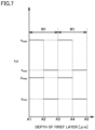
- the relation between the depth of the first layer and x or y is explained with use of Fig. 7 .
- the horizontal axis represents the depth of the first layer
- the vertical axis represents the concentration of x or y.
- the intersection point of the vertical axis and the horizontal axis is a spot nearest to the surface side of the coating film in the first layer.
- the intersection point represents a spot having a depth of 0 ⁇ m in the first layer.
- the spot having a depth of 0 ⁇ m in the first layer is represented as A1 in Fig. 7 .
- the x is the maximum value x max and the y is the maximum value y max ; and the region corresponds to region No. 1-1.
- the x is the minimum value x min and the y is the minimum value y min ; and the region corresponds to region No. 1-2.
- the x is the maximum value x max and the y is the maximum value y max ; and the region corresponds to region No. 1-1.
- the x is the minimum value x min and the y is the minimum value y min ; and the region corresponds to region No. 1-2.
- the sum total of the depth of a pair next to each other including region No. 1-1 and region No. 1-2, i.e., a distance W1 from a depth of 0 ⁇ m (A1) to a depth of A3 ⁇ m, or a distance W1 from a depth of A3 ⁇ m to a depth of A5 ⁇ m, corresponds to the period width.
- the respective period widths include a region No. 1-1 (not shown in drawing) and a region No. 1-2 (not shown in drawing) laminated along the thickness direction of the first layer.
- the x may be the minimum value x max
- the y may be the minimum value y min
- the x may be the minimum value x min
- the y may be the maximum value y max .
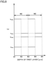
- the relation between the depth of the first layer and x or y is explained with use of Fig. 8 .
- the horizontal axis represents the depth of the first layer
- the vertical axis represents the concentration of x or y.
- the intersection point of the vertical axis and the horizontal axis is a spot nearest to the surface side of the coating film in the first layer.
- the intersection point represents a spot having a depth of 0 ⁇ m in the first layer.
- the spot having a depth of 0 ⁇ m in the first layer is represented as B1 in Fig. 8 .
- the x is the maximum value x max and the y is the minimum value y min , and the region corresponds to region No. 1-1.
- the x is the minimum value x min and the y is the maximum value y max ; and the region corresponds to region No. 1-2.
- the x is the maximum value x max and the y is the minimum value y min ; and the region corresponds to region No. 1-1.
- the x is the minimum value x min and the y is the maximum value y max ; and the region corresponds to region No. 1-2.
- the sum total of the depth of a pair next to each other including region No. 1-1 and region No. 1-2, i.e., a distance W2 from a depth of 0 ⁇ m (B1) to a depth of B3 ⁇ m, or a distance W2 from a depth of B3 ⁇ m to a depth of B5 ⁇ m, corresponds to the period width.
- the average of the crystallite size is preferably 5 nm or more and 90 nm or less.
- the film strength of the coating film including the first layer is further improved resulting from refinement of the crystallite size.
- reduction in toughness of the first layer caused by a too small crystallite size is suppressed, so that occurrence of cracks in the first layer may be suppressed.
- the lower limit of the average of the crystallite size is preferably 8 nm or more, more preferably 12 nm or more, and still more preferably 15 nm or more.
- the upper limit of the average of the crystallite size is 80 nm or less, more preferably 70 nm or less, and still more preferably 60 nm or less.
- the average of the crystallite size is preferably 8 nm or more and 80 nm or less, more preferably 12 nm or more and 70 nm or less, and still more preferably 15 nm or more and 60 nm or less.
- the average of the crystallite size may be determined by X-ray diffraction measurement (XRD measurement), for example, under the following conditions. Specifically, X-ray is irradiated to the surface of the coating film for the X-ray diffraction measurement (XRD measurement) to measure the full width half maximum (FWHM).
- the full width half maximum ⁇ is assigned to Scherrer's equation represented by the following (I) to derive crystallite size y.
- ⁇ K ⁇ / ⁇ cos ⁇ wherein K means a shape factor. In the present specification, K is "0.9".
- ⁇ means the wavelength of X-ray.
- ⁇ means the full width half maximum (FWHM) represented in radian unit.
- ⁇ means the Bragg angle of the (200) peak of the first layer.
- the measurement is performed at five spots optionally selected. Subsequently, the average of the crystallite size at the five measurement spots is calculated to determine the average of the crystallite size. Further, in the case where the coating film includes a surface layer (another layer), the XRD measurement is performed after exposure of the first layer.
- the residual stress in the first layer is preferably -3.0 GPa or more and -0.1 GPa or less. Thereby, the film strength of a cutting tool may be further improved.
- the lower limit of the residual stress in the first layer is preferably -2.8 GPa or more, more preferably -2.5 GPa or more, and still more preferably -2.2 GPa or more.
- the upper limit of the residual stress in the first layer is preferably -0.2 GPa or less, more preferably -0.3 GPa or less, and still more preferably -0.4 GPa or less.
- the residual stress in the first layer is preferably -2.8 GPa or more and -0.2 GPa or less, more preferably -2.5 GPa or more and -0.3 GPa or less, and still more preferably -2.5 GPa or more and -0.4 GPa or less.
- the residual stress means "compressive residual stress”.
- the residual stress may be determined by a 2 ⁇ -sin2 ⁇ method (side inclination method) with use of X-ray.
- the measurement conditions are as follows.
- the first layer is analyzed at three optional points on the flank face of the first layer by the 2 ⁇ -sin2 ⁇ method (side inclination method) with use of X-ray, and the average of the residual stresses obtained at these three points is determined as the residual stress in the first layer.
- the coating film includes a surface layer (another layer)
- the XRD measurement is performed after exposure of the first layer.
- a ratio of X-ray diffraction intensity I (200) of (200) plane of the first layer to the sum of I (200) , X-ray diffraction intensity I (111) of (111) plane of the first layer, and X-ray diffraction intensity I (220) of (220) plane of the first layer, I (200) /(I (200) + I (111) + I (220) ), is preferably 0.50 or more.
- X-ray diffraction intensity I (200) of (200) plane means the diffraction intensity (height of peak) of the highest peak among X-ray diffraction peaks derived from (200) plane (hereinafter, also referred to as "maximum diffraction intensity").
- maximum diffraction intensity means the sum of the maximum diffraction intensity (height of peak).
- the lower limit of I (200) /(I (200) +I (111) +I (220) ) is preferably 0.53 or more, more preferably 0.56 or more, and still more preferably 0.60 or more.
- the upper limit of I (200) /(I (200) +I (111) +I (220) ) is preferably 0.97 or less, more preferably 0.94 or less, and still more preferably 0.90 or less.
- I (200) /(I (200) +I (111) +I (220) ) is preferably 0.53 or more and 0.97 or less, more preferably 0.56 or more and 0.94 or less, and still more preferably 0.60 or more and 0.90 or less.
- I (200) , I (111) and I (220) may be determined by X-ray diffraction measurement (XRD measurement), for example, under the following conditions. Specifically, I (200) , I (111) and I (220) may be obtained by irradiating X-ray to the surface of the coating film to perform X-ray diffraction measurement (XRD measurement). The measurement is performed at five optionally selected spots on the flank face. Subsequently, the respective averages of I (200) , I (111) and I (220) at five spots are calculated. Subsequently, based on the average of I (200) , the average of I (111) and the average of I (220) , I (200) /(I (200) +I (111) +I (220) ) may be calculated.
- XRD measurement X-ray diffraction measurement
- the coating film further comprises a foundation layer, and the foundation layer preferably is composed of Ti a Al 1-a N or Al p Cr 1-p N.
- the foundation layer be disposed directly on the substrate and directly under the first layer. Thereby, the adhesion between the substrate and the coating film may be improved.
- the foundation layer has a thickness of preferably 0.05 ⁇ m or more and 1.0 ⁇ m or less. Thereby, the adhesion between the substrate and the coating film may be further improved.
- the reason is as follows. With a foundation layer having a too thin thickness, the adhesion between the substrate and the coating film tends to be hardly improved, and with a foundation layer having a too thick thickness, the improvement in the film strength resulting from the refinement of particles in the first layer tends to be hindered.
- the lower limit of the thickness of the foundation layer is preferably 0.10 ⁇ m or more, more preferably 0.15 ⁇ m or more, and still more preferably 0.20 ⁇ m or more.
- the upper limit of the thickness of the foundation layer is preferably 0.80 ⁇ m or less, more preferably 0.60 ⁇ m or less, and still more preferably 0.40 ⁇ m or less.
- the thickness of the foundation layer is preferably 0.10 ⁇ m or more and 0.80 ⁇ m or less, more preferably 0.15 ⁇ m or more and 0.60 ⁇ m or less, and still more preferably 0.20 ⁇ m or more and 0.40 ⁇ m or less.
- the a be 0.2 or more and 1.0 or less. Thereby, the adhesion to the substrate is improved, so that the peeling resistance of the coating film may be improved.
- the a is preferably 0.3 or more and 0.9 or less, more preferably 0.4 or more and 0.8 or less, and still more preferably 0.5 or more and 0.7 or less.
- the p be preferably 0 or more and 0.8 or less. Thereby, the adhesion to the substrate is improved, so that the peeling resistance of the coating film may be improved.
- the p is preferably 0.1 or more and 0.77 or less, more preferably 0.2 or more and 0.74 or less, and still more preferably 0.3 or more and 0.7 or less.
- the a and the p may be determined by the following method.
- a cutting tool is cut at an optional position to prepare a sample including a cross section of the coating film.
- a focused ion beam system, a cross section polisher, or the like may be used.
- the elemental analysis of the sample may be performed by energy dispersive X-ray spectroscopy (EDX) attached to SEM for the determination.
- EDX energy dispersive X-ray spectroscopy
- the coating film may further include other layers.
- examples of the other layers include an intermediate layer 14 and a surface layer 15.
- the coating film of the present embodiment may include intermediate layer 14, for example, between first layers 12 adjacent to each other ( Fig. 4 ), or between first layer 12 and surface layer 15 ( Fig. 5 ).
- Intermediate layer 14 is a layer disposed between first layer 12 and another first layer 12 or a layer other than first layer 12 (surface layer 15 or the like).
- the composition of the intermediate layer may be, for example, titanium nitride (TiN), titanium carbonitride (TiCN), titanium aluminum nitride (TiAlN), titanium aluminum silicon nitride (TiAlSiN), titanium aluminum boron nitride (TiAlBN), titanium aluminum zirconium nitride (TiAlZrN), titanium aluminum hafnium nitride (TiAlHfN), titanium aluminum vanadium nitride (TiAlVN), titanium aluminum niobium nitride (TiAlNbN), titanium aluminum tantalum nitride (TiAlTaN), titanium aluminum chromium nitride (TiAlCrN), titanium aluminum molybdenum nitride (TiAlMoN), or titanium aluminum tungsten nitride (TiAlWN).
- the thickness of the intermediate layer may be, for example, 0.2
- the coating film of the present embodiment may include a surface layer ( Fig. 6 ).
- Surface layer 15 is a layer disposed nearest to the surface side in coating film 40. However, the surface layer may not be formed at the cutting edge ridgeline.
- Examples of surface layer 15 include TiN layer. Since the TiN layer has a distinct color (exhibiting golden color), when used as surface layer 15, identification of the corner of a cutting insert after use for cutting (identification of used portion) is advantageously easy.
- the thickness of surface layer 15 may be, for example, 0.01 ⁇ m or more and 0.3 ⁇ m or less.
- a method for producing the cutting tool of embodiment 1 is described as follows. The following production method is an example, and the cutting tool in embodiment 1 may be produced by another method.
- the substrate is prepared.
- any substrate may be used as long as it is conventionally known as the substrate of this type.
- a base having a shape according to ISO standard DNGA150408, made of cemented carbide material (equivalent to K10) is prepared.
- Each of the cutting edge (corner) portions of the base is bonded to a substrate made of polycrystalline cubic boron nitride sintered material (shape: triangular prism having an isosceles triangle bottom with an apex angle of 55°, each of the sides of the angle having a length of 2 mm, and a thickness of 2 mm) so as to obtain a bonded body.
- shape triangular prism having an isosceles triangle bottom with an apex angle of 55°, each of the sides of the angle having a length of 2 mm, and a thickness of 2 mm
- a brazing material made of Ti-Zr-Cu is used for the bonding.
- the outer peripheral surface, top face and bottom face of the bonded body are ground to form a negative land shape (negative land width: 150 ⁇ m, negative land angle: 25°) at the cutting edge.
- a base having cutting edge (cutting blade) portions made of polycrystalline cubic boron nitride sintered materials, respectively, is obtained.
- a fine-grained grinding stone having a grit size of 700 or more for grinding the outer peripheral surface, the top face and the negative land portion of the bonded body.
- a grinding stone having a grit size of less than 700 irregularities caused from grinding streaks tend to occur, so that the absolute value of Rsk sub tends to increase.
- an Rsk sub having a certain value or more is preferred to improve adhesion between the substrate and the coating film.
- the present inventors have newly found that with an Rsk sub in the range of -2 or more and 2 or less, the surface of the substrate in contact with the coating film has a reduced skew of distribution of the ridges and valleys, so that adhesion between the substrate and the coating film may be improved, and further, the stress concentration caused by a load during processing is reduced, so that the peeling resistance of the coating film may be improved. Further, it has been newly found by the present inventors that with use of a fine-grained grinding stone having a grit size of 700 or more, Rsk sub may be controlled to the range of -2 or more and 2 or less.
- the surface of the substrate is ion bombarded.
- a base is set in a vacuum chamber of a film forming apparatus. Subsequently, the chamber is evacuated. Subsequently, the base is heated to 500°C, while rotating a rotary table at 3 rpm. Subsequently, Ar gas is introduced into the vacuum chamber, and a tungsten filament is discharged to generate Ar ions. A bias voltage is applied to the base, and the base is ion bombarded with Ar ions under the following conditions.
- the Rsk sub may be controlled to the range of -2 or more and 2 or less.
- Rsk sub may be controlled to the desired value.
- a coating film is formed on the substrate.
- the third step includes "covering with first layer” for covering at least a part of the surface of the ion bombarded substrate.
- Examples of the method for covering at least a part of the surface of the substrate with the first layer include a physical vapor deposition (PVD) method.
- PVD physical vapor deposition
- Examples of the PVD method include an AIP method (ion plating method for vaporizing solid material with use of vacuum arc discharge) and a sputtering method.
- AIP method ion plating method for vaporizing solid material with use of vacuum arc discharge
- a sputtering method In the case of producing a TiAlSiN layer by AIP method, a TiAlSi target as metal evaporation source and N 2 as reaction gas may be used.
- a TiAlSiN layer by sputtering method a TiAlSi target as metal evaporation source, N 2 as reaction gas, and a sputtering gas such as Ar, Kr and Xe as reaction gas may be used.
- the basal plate (substrate) temperature may be set to 300°C to 800°C, and the gas pressure may be set to 0.1 to 10 Pa.
- Covering with the first layer includes one or both of a step (i) of fluctuating the bias voltage during film forming and a step (ii) of performing simultaneous vapor deposition with two types of target compositions prepared.
- the step (i) may be performed, for example, by using a TiAlSi target as the target, and intermittently fluctuating the bias voltage between 35 V and 50 V.
- the step (ii) may be performed, for example, by using a TiAlSi target and a TiAlN target as two types of targets, and fixing the bias voltage at 30 V.
- the third step may include forming other layers such as a foundation layer and a surface layer in addition to covering with the first layer.
- the other layers may be formed by a conventional method.
- forming a foundation layer is referred to step (iii) in some cases.
- the surface of the coating film obtained in the third step is dry blasted.
- the fourth step is performed as follows.
- the rake face, flank face and negative land face of the coating film obtained in the third step are blasted with an elastic polishing medium including diamond abrasive grains from a projection distance of 100 mm at a projection angle adjusted to about 15 degrees to 70 degrees for 60 seconds to 120 seconds.
- an elastic polishing medium including diamond abrasive grains from a projection distance of 100 mm at a projection angle adjusted to about 15 degrees to 70 degrees for 60 seconds to 120 seconds.
- Ra surf may be controlled to 0 ⁇ m or more and 0.1 ⁇ m or less, and Rsk surf may be controlled to -2 or more and 2 or less.
- processing the surface of the coating film other than the steps described above may be appropriately performed by a method other than the fourth step.
- a base having a shape according to ISO standard DNGA150408, made of cemented carbide material (equivalent to K10) was prepared. Subsequently, the cutting edge (corner) portions of the base were bonded to a substrate made of polycrystalline cubic boron nitride sintered material (shape: triangular prism having an isosceles triangle bottom with an apex angle of 55°, each of the sides of the angle having a length of 2 mm, and a thickness of 2 mm) having a cBN content of 70%, with a binder composition including TiN, TiB 2 , Al 2 O 3 and AlN so as to obtain a bonded body.
- shape polycrystalline cubic boron nitride sintered material
- a brazing material made of Ti-Zr-Cu was used for the bonding.
- the outer peripheral surface, top face and bottom face of the bonded body were ground to form a negative land shape (negative land width: 150 ⁇ m, negative land angle: 25°) at the cutting edge. Grinding was performed using a grinding stone having a grit size shown in the column "grinding stone" of "first step” in Table 1 and Table 2. Thus, a base having cutting edge (cutting blade) portions made of polycrystalline cubic boron nitride sintered materials, respectively, was obtained.
- the base was set in a vacuum chamber of a film forming apparatus. Subsequently, the chamber was evacuated. Subsequently, the base was heated to 500°C, while rotating a rotary table at 3 rpm. Subsequently, Ar gas was introduced into the vacuum chamber (pressure: 1 Pa), and a tungsten filament was discharged to generate Ar ions. A bias voltage was applied to the base, and the base was ion bombarded with the Ar ions. The bias voltage and the time for ion bombardment are as shown in columns "Bias voltage” and “Time” of "Second step" in Table 1 and Table 2.
- step (iii) was performed under conditions with use of a target described in column “Target” of "Forming foundation layer” in Table 2, and at a bias voltage described in column “Bias voltage” of "Forming foundation layer” in Table 2.
- a first layer was formed on the surface of the substrate or the foundation layer.
- the step (i) was performed for samples No. 1 to No. 10, and the step (ii) was performed for samples No. 11 to No. 48, and samples No. 101 to No. 104.
- step (i) by using the target described in column “Target” of “Step (i)” of “Covering with first layer” in Table 1 and Table 2, and N 2 gas as reaction gas, covering with first layer was performed at the bias voltage described in column “Bias voltage".
- the description 30/150 in column “Bias voltage” means that the bias voltage was intermittently switched between 30 V and 150 V. More specifically, a single period in which the bias voltage maintained at 30 V for 120 seconds and then switched to 150 V to be maintained for 120 seconds was repeated. In other words, the single period time was 240 seconds.
- step (ii) by using the two types of targets described in column “Target” of “Step (ii)” of “Covering with first layer” in Table 1 and Table 2, and N 2 gas as reaction gas, covering with first layer was performed at the bias voltage described in column “Bias voltage".
- TiAlSi and TiAl were used as the targets, N 2 gas was used as reaction gas, and the bias voltage was set to 30 V.
- both of the two targets are "TiAlB" targets.
- composition ratio of the targets is different as follows.
- the surface to be processed (rake face, flank face and negative land face) on the surface of the coating film obtained in third step was blasted under conditions described in Table 1 and Table 2.
- the rake face, flank face and negative land face of the coating film were blasted with an elastic polishing medium including diamond abrasive grains from a projection distance of 100 mm at a projection angle adjusted to about 15 degrees to 70 degrees for 60 seconds.
- Respective properties of cutting tools of samples No. 1 to No. 48 and samples No. 101 to No. 104 were evaluated as follows. Cutting tools of samples No. 1 to No. 48 correspond to Examples, and cutting tools of samples No. 101 to No. 104 correspond to Comparative Examples.
- the thickness of the first layer was determined by the method described in embodiment 1. The results obtained are described in item “Thickness of first layer [ ⁇ m]” in Table 3 and Table 4, respectively. Further, with regard to the cutting tools of samples No. 40 to No. 45, the thickness of the foundation layer was determined by the method described in embodiment 1. The results obtained are described in item “Thickness of foundation layer [ ⁇ m]” in Table 3 and Table 4, respectively.
- the cutting conditions correspond to high efficiency processing.
- Samples No. 1 to No. 48 correspond to Examples.
- Samples No. 101 to No. 104 correspond to Comparative Examples. From the results in Table 3 and Table 4, it has been found that the cutting tools of samples No. 1 to No. 48 corresponding to Examples have a longer tool life even in high efficiency processing than the cutting tools of samples No. 101 to No. 104 corresponding to Comparative Examples.
- rake face 1: rake face, 2: flank face, 3: cutting edge ridgeline, 10: cutting tool, 11: substrate, 12: first layer, 13: foundation layer, 14: intermediate layer, 15: surface layer, 40: coating film, w1 and w2: period width, a1 to a5 and b1 to b5: depth of first layer, l1: average line
Landscapes
- Chemical & Material Sciences (AREA)
- Engineering & Computer Science (AREA)
- Mechanical Engineering (AREA)
- Chemical Kinetics & Catalysis (AREA)
- Materials Engineering (AREA)
- Metallurgy (AREA)
- Organic Chemistry (AREA)
- Inorganic Chemistry (AREA)
- Cutting Tools, Boring Holders, And Turrets (AREA)
- Drilling Tools (AREA)
- Physical Vapour Deposition (AREA)
Abstract
A cutting tool comprising a substrate and a coating film disposed on the substrate, wherein the coating film comprises a first layer; the first layer has a thickness of 0.2 µm or more and 9 µm or less; the first layer is composed of Ti(1-x-y)AlxMyN, wherein M is at least one element selected from the group consisting of zirconium, hafnium, a group V element in the periodic table, a group VI element, silicon and boron; in the first layer, x and y change along the thickness direction of the first layer; a maximum value of x, xmax, is 0.20 or more and 0.70 or less; a minimum value of x, xmin, is 0 or more and 0.6 or less; xmax and xmin satisfy 0.01 ≤ xmax - xmin ≤ 0.7; a maximum value of y, ymax, is 0.01 or more and 0.20 or less; a minimum value of y, ymin, is 0 or more and 0.19 or less; and ymax and ymin satisfy 0.01 ≤ ymax - ymin ≤ 0.2.
Description
- The present disclosure relates to a cutting tool.
- In order to extend the service life of cutting tools, various studies have been made. In
Japanese Patent Laying-Open No. 8-119774 WO 2021/085253 (Patent Literature 2), a surface-coated cutting tool having a tool base made of polycrystalline cubic boron nitride sintered material and a hard coating layer on the surface of the tool base is disclosed. The hard coating layer has a lower layer (AlTiN layer) directly on the tool base, and an upper layer (AlTiBN layer) on the lower layer, and the upper layer has a compositionally modulated structure in which the boron concentration repeatedly changes along the layer thickness direction. -
- PTL 1:
Japanese Patent Laying-Open No. 8-119774 - PTL 2:
WO 2021/085253 - A cutting tool of the present disclosure relates to a cutting tool comprising a substrate and a coating film disposed on the substrate, wherein
- the coating film comprises a first layer;
- the first layer has a thickness of 0.2 µm or more and 9 µm or less;
- the first layer is composed of Ti(1-x-y)AlxMyN,
- wherein M is at least one element selected from the group consisting of zirconium, hafnium, a group V element in the periodic table, a group VI element, silicon and boron;
- in the first layer, x and y change along a thickness direction of the first layer;
- a maximum value of x, xmax, is 0.20 or more and 0.70 or less;
- a minimum value of x, xmin, is 0 or more and 0.6 or less;
- xmax and xmin satisfy 0.01 ≤ xmax - xmin ≤ 0.7,
- a maximum value of y, ymax, is 0.01 or more and 0.20 or less;
- a minimum value of y, ymin, is 0 or more and 0.19 or less; and
- ymax and ymin satisfy 0.01 ≤ ymax - ymin ≤ 0.2.
-
-
Fig. 1 is a perspective view showing an aspect of a cutting tool of the present disclosure. -
Fig. 2 is a schematic cross-sectional view showing an aspect of a cutting tool of the present disclosure. -
Fig. 3 is a schematic cross-sectional view showing another aspect of a cutting tool of the present disclosure. -
Fig. 4 is a schematic cross-sectional view further showing another aspect of a cutting tool of the present disclosure. -
Fig. 5 is a schematic cross-sectional view showing another different aspect of a cutting tool of the present disclosure. -
Fig. 6 is a schematic cross-sectional view further showing another different aspect of a cutting tool of the present disclosure. -
Fig. 7 is a graph showing the relationship between the depth of the first layer and x or y in an aspect of the cutting tool of the present disclosure. -
Fig. 8 is a graph showing the relationship between the depth of the first layer and x or y in another aspect of the cutting tool of the present disclosure. -
Fig. 9 is a diagram illustrating the relationship between the surface irregularity and skewness. -
Fig. 10 is a diagram illustrating the relationship between the surface irregularity and skewness. - In recent years, needs of high-efficiency processing has been enhanced. Along with the needs, a cutting tool having a long tool life has been required even in high-efficiency processing.
- Accordingly, an object of the present disclosure is to provide a cutting tool having a long tool life even in high-efficiency processing.
- According to the present disclosure, a cutting tool having a long tool life may be provided even in high-efficiency processing.
- First, embodiments of the present disclosure are listed and explained.
- (1) A cutting tool comprises a substrate and a coating film disposed on the substrate, wherein
- the coating film comprises a first layer;
- the first layer has a thickness of 0.2 µm or more and 9 µm or less;
- the first layer is composed of Ti(1-x-y)AlxMyN,
- wherein M is at least one element selected from the group consisting of zirconium, hafnium, a group V element in the periodic table, a group VI element, silicon and boron;
- in the first layer, x and y change along a thickness direction of the first layer;
- a maximum value of x, xmax, is 0.20 or more and 0.70 or less;
- a minimum value of x, xmin, is 0 or more and 0.6 or less;
- xmax and xmin satisfy 0.01 ≤ xmax - xmin ≤ 0.7,
- a maximum value of y, ymax, is 0.01 or more and 0.20 or less;
- a minimum value of y, ymin, is 0 or more and 0.19 or less; and
- ymax and ymin satisfy 0.01 ≤ ymax - ymin ≤ 0.2.
- The cutting tool of the present disclosure may have a long tool life even in high-efficiency processing.
- (2) In the first layer, an average of crystallite size is preferably 5 nm or more and 90 nm or less. Thereby, the film strength of the coating film is further improved. Further, occurrence of cracks in the first layer is suppressed.
- (3) The coating film further comprises a foundation layer;
- wherein the foundation layer is disposed directly on the substrate and directly under the first layer;
- the foundation layer has a thickness of 0.05 µm or more and 1.0 µm or less;
- the foundation layer comprises TiaAl1-aN or AlpCr1-pN;
- a is 0.2 or more and 1.0 or less,
- and p is preferably 0 or more and 0.8 or less. Thereby, the adhesion between the substrate and the coating film of the cutting tool is improved.
- (4) The first layer has a residual stress of preferably -3.0 GPa or more and -0.1 GPa or less. Thereby, the film strength of the coating film is further improved.
- (5) A roughness of a surface of the coating film, Rasurf, is preferably 0 µm or more and 0.1 µm or less. Thereby, the peeling resistance of the coating film is improved.
- (6) A skewness of a surface of the coating film, Rsksurf, is preferably -2 or more and 2 or less. Thereby, the peeling resistance of the coating film is further improved.
- (7) A skewness of a surface of the substrate in contact with the coating film, Rsksub, is preferably -2 or more and 2 or less. Thereby, the peeling resistance of the coating film is further improved.
- (8) A ratio of X-ray diffraction intensity I(200) of (200) plane of the first layer to a sum of I(200), X-ray diffraction intensity I(111) of (111) plane of the coating film, and X-ray diffraction intensity I(220) of (220) plane of the coating film, I(200)/(I(200) + I(111)+ I(220)), is preferably 0.50 or more. Thereby, the peeling resistance of the coating film is further improved.
- A specific example of the cutting tool in an embodiment of the present disclosure (hereinafter also referred to as "present embodiment") is explained with reference to drawings. In the drawings of the present disclosure, the same reference sign represents the same part or a corresponding part. Dimensions such as length, width, thickness, depth, etc., are appropriately changed for clarification and simplification of drawings, not necessarily representing actual dimensions.
- In the present specification, an expression in the form of "A to B" means to include the upper limit and the lower limit of a range (in other words, A or more and B or less). In the case where A has no unit added while B has a unit added, the unit of A and the unit of B are the same.
- In the present specification, in the case where a compound or the like is represented by a chemical formula without particular limitation on the atomic ratio, all the conventionally known atomic ratios are included, not necessarily limited to the stoichiometric range alone. For example, a description "TiAlSiN" allows the ratio of the number of atoms constituting TiAlSiN to include all the conventionally known atomic ratios.
- In the present specification, individual planes in crystallographic description are represented in ().
- As shown in
Fig. 2 to Fig. 6 , acutting tool 10 of the present embodiment comprises asubstrate 11 and acoating film 40 disposed onsubstrate 11; -
coating film 40 comprises afirst layer 12; -
first layer 12 has a thickness of 0.2 µm or more and 9 µm or less; -
first layer 12 is composed of Ti(1-x-y)AlxMyN, - wherein M is at least one element selected from the group consisting of zirconium, hafnium, a group V element in the periodic table, a group VI element, silicon and boron;
- in
first layer 12, x and y change along the thickness direction offirst layer 12; - a maximum value of x, xmax, is 0.20 or more and 0.70 or less;
- a minimum value of x, xmin, is 0 or more and 0.6 or less;
- xmax and xmin satisfy 0.01 ≤ xmax - xmin ≤ 0.7,
- a maximum value of y, ymax, is 0.01 or more and 0.20 or less;
- a minimum value of y, ymin, is 0 or more and 0.19 or less; and
- ymax and ymin satisfy 0.01 ≤ ymax - ymin ≤ 0.2.
- The cutting tool of the present disclosure may have a long tool life even in high-efficiency processing. The reason is presumed as follows.
- In
first layer 12, x and y change along the thickness direction offirst layer 12, a maximum value of x, xmax, is 0.20 or more and 0.70 or less, a minimum value of x, xmin, is 0 or more and 0.6 or less, xmax and xmin satisfy 0.01 ≤ xmax - xmin ≤ 0.7, a maximum value of y, ymax, is 0.01 or more and 0.20 or less, a minimum value of y, ymin, is 0 or more and 0.19 or less, and ymax and ymin satisfy 0.01 ≤ ymax - ymin ≤ 0.2. As a result, grain growth infirst layer 12 is suppressed, because the lattice constants of Ti(1-x-y)AlxMyN are hardly equalized. Accordingly, infirst layer 12, fine texture may be formed. As a result, cuttingtool 10 havingcoating film 40 includingfirst layer 12 has excellent film strength, so that a long tool life may be achieved even in high-efficiency processing. - The shape and use of cutting
tool 10 of the present embodiment are not particularly limited. Examples of the shape of cuttingtool 10 of the present embodiment include a drill, an end mill, an indexable cutting insert for drilling, an indexable cutting insert for end milling, an indexable cutting insert for milling, an indexable cutting insert for lathe turning, a metal saw, a gear cutting tool, a reamer, a tap, and a tip for pin milling of a crankshaft. -
Fig. 1 is a perspective view showing an aspect of acutting tool 10 of the present disclosure. Cuttingtool 10 in such a shape is used as an indexable cutting insert such as an indexable cutting insert for lathe turning. - Further, cutting
tool 10 of the present embodiment is not limited to one having a structure in which the whole of cuttingtool 10 includes asubstrate 11 and acoating film 40 formed onsubstrate 11 as shown inFig. 1 alone, but includes one having the structure in a part of cutting tool 10 (in particular, cutting edge (cutting blade), etc.) only. For example, one in which the cutting edge portion alone of the base (support) made of cemented carbide or the like has the structure is also included in the cutting tool of the present embodiment. In that case, literally, the cutting edge portion is presumed to be the cutting tool. In other words, even in the case where the structure occupies only a part of the cutting tool, the structure is referred to as the cutting tool. - As the substrate of the present embodiment, a conventionally known substrate of this type may be used without any particular limitation. Examples thereof include a cemented carbide (for example, a tungsten carbide (WC)-based cemented carbide, a cemented carbide containing Co in addition to WC, and a cemented carbide with addition of a carbonitride of Ti, Ta, Nb, etc., in addition to WC), a cermet (containing TiC, TiN, TiCN or the like as main component), a high-speed steel, a tool steel, ceramics (titanium carbide (TiC), silicon carbide (SiC), silicon nitride (SiN), Aluminum nitride (AlN), aluminum oxide (Al2O3), sialon, and mixture thereof), a polycrystalline cubic boron nitride sintered material (cBN sintered material), a diamond sintered material, and a hard material with polycrystalline cubic boron nitride particles dispersed in a binder phase.
- Among these various substrates, a polycrystalline cubic boron nitride sintered material is particularly preferably selected. The reason is that the polycrystalline cubic boron nitride sintered material exhibits particularly excellent abrasion resistance in cutting of an iron-based high-hardness material, having suitability for a substrate of cutting tools for the use.
- In the case where a cemented carbide is used as substrate, the cemented carbide exhibits the effect of the present embodiment even when containing free carbon or an abnormal phase referred to as η phase in the texture. The substrate for use of the present embodiment allows the surface to be a modified surface. For example, a cemented carbide may have a de-β layer formed on the surface, and a cBN sintered material may have a surface hardened layer. Even with such modification of the surface, the effect of the present embodiment may be exhibited.
- In the case where the cutting tool is an indexable cutting insert (indexable cutting insert for lathe turning, an indexable cutting insert for milling, etc.), the substrate may include one having a tip breaker or one having no tip breaker. The shape of the cutting edge may include any one of a sharp edge (a ridge at which a rake face and a flank face cross), a honed shape (rounded sharp edge), a negative land (chamfered shape), and a combined shape of a honed shape and a negative land.
- The skewness of a surface of the substrate in contact with the coating film, Rsksub, is preferably -2 or more and 2 or less. The term "skewness" means the skewness of the roughness curve specified in JIS B 0601-2001, which is a parameter representing the degree of distortion of ridges and valleys of a plane. In other words, the term "skewness" is an index representing the symmetricalness of the ridges and valleys relative to an average line L1 as center as shown in
Fig. 9 and Fig. 10 . In the case where the plane is skewed to the upper side relative to average line L1, the "skewness" has a positive value (Fig. 9 ). In contrast, in the case where the plane is skewed to the lower side relative to average line L1, the "skewness" has a negative value (Fig. 10 ). Further, in the case where the probability density distribution curve shown inFig. 9 or Fig. 10 follows a normal distribution, the skewness has a value of "0". - In the case where the skewness of the surface of the substrate in contact with the coating film, Rsksub, is -2 or more and 2 or less, the surface of the substrate in contact with the coating film has a reduced skew of distribution of the ridges and valleys. As a result, the adhesion between the substrate and the coating film may be improved. The surface of the substrate in contact with the coating film has a reduced skew of distribution of the ridges and valleys. As a result, the stress concentration caused by a load during processing is reduced, so that the peeling resistance of the coating film may be improved. The relations between the skewness Rsksub and adhesion between the substrate and the coating film, and between the skewness Rsksub and the peeling resistance of the coating film have been newly found by the present inventors.
- The lower limit of the Rsksub is more preferably -1.8 or more, still more preferably -1.6 or more, and furthermore preferably -1.4 or more. The upper limit of the Rsksub is more preferably 1.8 or less, still more preferably 1.6 or less, and furthermore preferably 1.4 or less. Further, the Rsksub is more preferably -1.8 or more and 1.8 or less, still more preferably -1.6 or more and 1.6 or less, and furthermore preferably -1.4 or more and 1.4 or less.
- The skewness of a surface of the substrate in contact with the coating film, Rsksub, may be determined, for example, by the following method. First, a cutting tool is cut along the normal direction of the flank face with the cutting edge included to expose the cross section. The cutting may be performed using a focused ion beam system, a cross section polisher, or the like. Using a scanning electron microscope (SEM), the cross section is observed with a magnifying power of 2000 to obtain a backscattered electron image. Subsequently, using an image processing software (e.g., trade name "Winroof" manufactured by Mitani Corporation), the backscattered electron image is magnified 2.5 times to obtain a field of view. Subsequently, in the field of view, any optional 50 µm-square spot including "surface of coating film" and "face in contact with the coating film of a substrate (corresponding to the interface between the substrate and the coating film)" is selected to trace the "face of the substrate in contact with the coating film" as a line for extraction. The extracted line is converted into numerical values using an image processing software (e.g., trade name "Winroof" manufactured by Mitani Corporation) to calculate the average of the numerical values. Here, expression "converting a line into numerical values" means that when the extracted line is placed on an x-y coordinate axis, the y-axis values of the line are outputted in the x-axis direction at 0.05 µm intervals. Subsequently, based on the average, an average line is drawn in the direction approximately parallel with the face of the substrate in contact with the coating film. Subsequently, in coordinate axes with the average line as X-axis, and with the vertical direction to the X-axis as Y-axis, the face roughness curve Z (x) at the surface of the coating film is obtained using the image processing software. Subsequently, Z (x) is assigned to the following formula (1) to obtain Rq. Here, "l" is "50 µm".
[Expression 1]
- Subsequently, Z(x) and Rq are assigned to the following formula (2) to obtain skewness Rsk.
[Expression 2]
- The above procedure is performed for five optional fields of view in the cross section to obtain the Rsk, of which average is calculated to determine the skewness Rsksub.
-
Coating film 40 is disposed on substrate 11 (Fig. 2 to Fig. 6). Fig. 2 to Fig. 6 are schematic cross-sectional views showing an aspect of the cutting tool of the present disclosure. "Coating film" covers at least the cutting edge ofsubstrate 11, so that various properties such as peeling resistance, breakage resistance and abrasion resistance of a cutting tool are improved. The cutting edge described herein means a region within 500 µm from the cutting edge ridgeline along the substrate surface. It is preferable that coatingfilm 40 cover whole the surface ofsubstrate 11. However, the case where a part ofsubstrate 11 is not covered withcoating film 40, or the structure ofcoating film 40 is partly different is included within the scope of the present embodiment. - The thickness of the coating film is preferably 0.4 µm or more and 8 µm or less, more preferably 0.6 µm or more and 7 µm or less, still more preferably 0.8 µm or more and 6 µm or less, furthermore preferably 1.0 µm or more and 5 µm or less, and particularly preferably 1.2 µm or more and 4 µm or less. The thickness of the coating film means the sum total of the respective thicknesses of the layers that constitute the coating film. Examples of the "layers that constitute the coating film" include the first layer, the foundation layer, and another layer that is described as a layer other than the first layer and the foundation layer in the following.
- The thickness of the coating film may be determined as follows. First, a cutting tool is cut at an optional position to prepare a sample including the cross section of the coating film. For the preparation of the sample, a focused ion beam system, a cross section polisher, etc. may be used. Subsequently, the prepared cross section is observed with a scanning electron microscope, with the magnification power being adjusted to include the whole region in the thickness direction of the coating film in the observed image. Subsequently, the thickness is observed at five points, and the average thereof is determined as the thickness of the coating film. The measurement of the thickness of the first layer, the foundation layer or the other layer is performed in the same manner.
-
Coating film 40 includesfirst layer 12. In an aspect of the present embodiment, a plurality offirst layers 12 may be disposed as long as the effect that the cutting tool exhibits is maintained. Thereby, even when a part of the coating film is worn, the first layer remains in the coating film, so that the cutting tool may retain excellent film strength. The expression "including the first layer" means that the coating film may include the foundation layer and another layer other than the first layer and the foundation layer described in the following, in addition to the first layer. - The skewness of a surface of the coating film, Rsksurf, is preferably -2 or more and 2 or less. Thereby, the surface of the coating film has a reduced skew of distribution of the ridges and valleys. As a result, the stress concentration caused by a load during processing is reduced, so that the peeling resistance of the coating film may be improved. The lower limit of the Rsksurf is more preferably -1.8 or more, still more preferably -1.6 or more, and furthermore preferably -1.4 or more. The upper limit of the Rsksurf is more preferably 1.8 or less, still more preferably 1.6 or less, and furthermore preferably 1.4 or less. Further, the Rsksurf is more preferably -1.8 or more and 1.8 or less, still more preferably -1.6 or more and 1.6 or less, and furthermore preferably -1.4 or more and 1.4 or less.
- The roughness of a surface of the coating film, Rasurf, is preferably 0 µm or more and 0.1 µm or less. Thereby, irregularities on the surface of the coating film is reduced. As a result, the stress concentration caused by a load during processing is reduced, so that the peeling resistance of the coating film may be improved. The lower limit of the Rasurf is preferably 0.01 µm or more, more preferably 0.02 µm or more, and still more preferably 0.03 µm or more. The upper limit of the Rasurf is preferably 0.09 µm or less, more preferably 0.08 µm or less, and still more preferably 0.07 µm or less. Further, the Rasurf is preferably 0.01 µm or more and 0.09 µm or less, more preferably 0.02 µm or more and 0.08 µm or less, and still more preferably 0.03 µm or more and 0.08 µm or less. The term "surface roughness Ra" means the arithmetic average roughness specified in JIS B 0601-2001.
- The roughness of a surface of the coating film, Rasurf, is measured by the following procedure. On the rake face in the region within a distance of 1000 µm from the cutting edge, a 400 µm-square measurement region is set. The surface roughness of the measurement region is measured with a stylus-type surface profile meter. By the same procedure, the surface roughness is measured in a measurement region at five optional spots. The average of the surface roughness at the five spots is calculated to determine the roughness of a surface of the coating film, Rasurf. It is to be noted that the "skewness of a surface of the coating film, Rsksurf" is also determined by the same method.
- The first layer preferably has a thickness of 0.2 µm or more and 9 µm or less. Thereby, the film strength of the coating film is improved. As a result, the film strength of the coating film may be improved. The lower limit of the thickness of the first layer is preferably 0.4 µm or more, more preferably 0.6 µm or more, and still more preferably 0.8 µm or more. The upper limit of the thickness of the first layer is preferably 8 µm or less, more preferably 7 µm or less, and still more preferably 6 µm or less. Further, the thickness of the first layer is preferably 0.4 µm or more and 8 µm or less, more preferably 0.6 µm or more and 7 µm or less, and still more preferably 0.8 µm or more and 6 µm or less.
- The first layer is composed of Ti(1-x-y)AlxMyN, wherein M is at least one element selected from the group consisting of zirconium, hafnium, a group V element in the periodic table, a group VI element, silicon and boron. Thereby, the first layer may have excellent strength.
- In
first layer 12, x and y change along the thickness direction offirst layer 12; a maximum value of x, xmax, is 0.20 or more and 0.70 or less; a minimum value of x, xmin, is 0 or more and 0.6 or less; xmax and xmin satisfy 0.01 ≤ xmax - xmin ≤ 0.7; a maximum value of y, ymax, is 0.01 or more and 0.20 or less; a minimum value of y, ymin, is 0 or more and 0.19 or less; and ymax and ymin satisfy 0.01 ≤ ymax - ymin ≤ 0.2. As a result, grain growth infirst layer 12 is suppressed, because the lattice constants of Ti(1-x-y)AlxMyN are hardly equalized. Accordingly, infirst layer 12, fine texture may be formed. As a result, cuttingtool 10 havingcoating film 40 includingfirst layer 12 may have excellent film strength. - The lower limit of the xmax is preferably 0.25 or more, more preferably 0.3 or more, and still more preferably 0.35 or more. The upper limit of the xmax is preferably 0.65 or less, more preferably 0.6 or less, and still more preferably 0.55 or less. The xmax is preferably 0.25 or more and 0.65 or less, more preferably 0.3 or more and 0.6 or less, and still more preferably 0.35 or more and 0.55 or less.
- The lower limit of the xmin is preferably 0.05 or more, more preferably 0.1 or more, and still more preferably 0.15 or more. The upper limit of the xmin is preferably 0.57 or less, more preferably 0.54 or less, and still more preferably 0.50 or less. The xmin is preferably 0.05 or more and 0.57 or less, more preferably 0.1 or more and 0.54 or less, and still more preferably 0.15 or more and 0.50 or less.
- The lower limit of the ymax is preferably 0.015 or more, more preferably 0.02 or more, and still more preferably 0.025 or more. The upper limit of the ymax is preferably 0.18 or less, more preferably 0.16 or less, and still more preferably 0.14 or less. The ymax is preferably 0.015 or more and 0.18 or less, more preferably 0.02 or more and 0.16 or less, and still more preferably 0.025 or more and 0.14 or less.
- The lower limit of the ymin is preferably 0.005 or more, more preferably 0.01 or more, and still more preferably 0.015 or more. The upper limit of the ymin is preferably 0.17 or less, more preferably 0.15 or less, and still more preferably 0.13 or less. The ymin is preferably 0.005 or more and 0.17 or less, more preferably 0.01 or more and 0.15 or less, and still more preferably 0.015 or more and 0.13 or less.
- The lower limit of the xmax-xmin is preferably 0.05 or more, more preferably 0.1 or more, and still more preferably 0.15 or more. The upper limit of the xmax-xmin is preferably 0.6 or less, more preferably 0.5 or less, and still more preferably 0.4 or less. The xmax-xmin is preferably 0.05 or more and 0.6 or less, more preferably 0.1 or more and 0.5 or less, and still more preferably 0.15 or more and 0.4 or less.
- The lower limit of the ymax-ymin is preferably 0.015 or more, more preferably 0.02 or more, and still more preferably 0.025 or more. The upper limit of the ymax-ymin is preferably 0.18 or less, more preferably 0.16 or less, and still more preferably 0.15 or less. The ymax-ymin is preferably 0.015 or more and 0.18 or less, more preferably 0.02 or more and 0.16 or less, and still more preferably 0.025 or more and 0.15 or less.
- The xmax, xmin, ymax and ymin may be determined as follows. First, the type and atomic content ratio of the element represented by M in Ti(1-x-y)AlxMyN that constitutes the first layer, and the atomic content ratio of Al are measured by Auger electron spectroscopy along the thickness direction of the first layer from the flank face side of the coating film. The analysis conditions and the conditions for ion sputtering (Ar+) are as follows.
-
- Energy of primary electron: 10 keV
- Electric current: about 3 nA
- Incident angle: 0 degree relative normal line of flank face of sample
- Analysis region: about 10 µm by 10 µm
-
- Energy: 1 keV
- Incident angle: about 0 degree relative to normal line of flank face of sample
- Sputtering rate: about 2 nm/min
- The measurement is performed at five optional points. From the average of the measured values of the atomic content ratio at the five points, xmax, xmin, ymax and ymin are determined. Further, the type of element represented by M is identified.
- In the present specification, the expression "in the first layer, x and y change along the thickness direction of the first layer" is a concept including an aspect in which "in the first layer, x and y periodically change along the thickness direction of the first layer at the same period width" and an aspect other than the aspect in which "in the first layer, x and y periodically change along the thickness direction of the first layer at the same period width".
- In the case where in the first layer, x and y periodically change along the thickness direction of the first layer at the same period width, the average of the period width may be 1 nm or more and 500 nm or less. The average of the period width is determined by plotting the xmax, xmin, ymax and ymin in a graph with the horizontal axis representing the depth of the first layer and the vertical axis representing the concentration of x or y so as to identify the periodicity of x or y.
- In the case where in the first layer, x and y periodically change along the thickness direction of the first layer at the same period width, the xmax, and the ymax are preferably the maximum value of x and the maximum value of y of the period width, respectively. The xmin, and the ymin are preferably the minimum value of x and the minimum value of y of the period width, respectively. Thereby, in
first layer 12, a finer texture may be formed. As a result, cuttingtool 10 havingcoating film 40 includingfirst layer 12 may have more excellent film strength. - In the cutting tool of the present embodiment, the respective period widths include a region No. 1-1 (not shown in drawing) and a region No. 1-2 (not shown in drawing) laminated along the thickness direction of the first layer. In region No. 1-1, the x may be the maximum value xmax, and the y may be the maximum value ymax, and in region No. 1-2, the x may be the minimum value xmin, and the y may be the minimum value ymin. In this case, the relation between the depth of the first layer and x or y is explained with use of
Fig. 7 . - In the graph of
Fig. 7 , the horizontal axis represents the depth of the first layer, and the vertical axis represents the concentration of x or y. The intersection point of the vertical axis and the horizontal axis is a spot nearest to the surface side of the coating film in the first layer. In other words, the intersection point represents a spot having a depth of 0 µm in the first layer. The spot having a depth of 0 µm in the first layer is represented as A1 inFig. 7 . In the region ranging from a depth of 0 µm (A1) to a depth of A2 µm, the x is the maximum value xmax and the y is the maximum value ymax; and the region corresponds to region No. 1-1. In the region ranging from a depth of A2 µm to a depth of A3 µm, the x is the minimum value xmin and the y is the minimum value ymin; and the region corresponds to region No. 1-2. Further, in the region ranging from a depth of A3 µm to a depth of A4 µm, the x is the maximum value xmax and the y is the maximum value ymax; and the region corresponds to region No. 1-1. In the region ranging from a depth of A4 µm to a depth of A5 µm, the x is the minimum value xmin and the y is the minimum value ymin; and the region corresponds to region No. 1-2. - In
Fig. 7 , the sum total of the depth of a pair next to each other including region No. 1-1 and region No. 1-2, i.e., a distance W1 from a depth of 0 µm (A1) to a depth of A3 µm, or a distance W1 from a depth of A3 µm to a depth of A5 µm, corresponds to the period width. - In the cutting tool of the present embodiment, the respective period widths include a region No. 1-1 (not shown in drawing) and a region No. 1-2 (not shown in drawing) laminated along the thickness direction of the first layer. In region No. 1-1, the x may be the minimum value xmax, and the y may be the minimum value ymin, and in region No. 1-2, the x may be the minimum value xmin, and the y may be the maximum value ymax. In this case, the relation between the depth of the first layer and x or y is explained with use of
Fig. 8 . - In the graph of
Fig. 8 , the horizontal axis represents the depth of the first layer, and the vertical axis represents the concentration of x or y. The intersection point of the vertical axis and the horizontal axis is a spot nearest to the surface side of the coating film in the first layer. In other words, the intersection point represents a spot having a depth of 0 µm in the first layer. The spot having a depth of 0 µm in the first layer is represented as B1 inFig. 8 . In the region ranging from a depth of 0 µm (B1) to a depth of B2 µm, the x is the maximum value xmax and the y is the minimum value ymin, and the region corresponds to region No. 1-1. In the region ranging from a depth of B2 µm to a depth of B3 µm, the x is the minimum value xmin and the y is the maximum value ymax; and the region corresponds to region No. 1-2. Further, in the region ranging from a depth of B3 µm to a depth of B4 µm, the x is the maximum value xmax and the y is the minimum value ymin; and the region corresponds to region No. 1-1. In the region ranging from a depth of B4 µm to a depth of B5 µm, the x is the minimum value xmin and the y is the maximum value ymax; and the region corresponds to region No. 1-2. - In
Fig. 8 , the sum total of the depth of a pair next to each other including region No. 1-1 and region No. 1-2, i.e., a distance W2 from a depth of 0 µm (B1) to a depth of B3 µm, or a distance W2 from a depth of B3 µm to a depth of B5 µm, corresponds to the period width. - In the first layer, the average of the crystallite size is preferably 5 nm or more and 90 nm or less. Thereby, the film strength of the coating film including the first layer is further improved resulting from refinement of the crystallite size. Further, reduction in toughness of the first layer caused by a too small crystallite size is suppressed, so that occurrence of cracks in the first layer may be suppressed. Further, the lower limit of the average of the crystallite size is preferably 8 nm or more, more preferably 12 nm or more, and still more preferably 15 nm or more. The upper limit of the average of the crystallite size is 80 nm or less, more preferably 70 nm or less, and still more preferably 60 nm or less. The average of the crystallite size is preferably 8 nm or more and 80 nm or less, more preferably 12 nm or more and 70 nm or less, and still more preferably 15 nm or more and 60 nm or less.
- The average of the crystallite size may be determined by X-ray diffraction measurement (XRD measurement), for example, under the following conditions. Specifically, X-ray is irradiated to the surface of the coating film for the X-ray diffraction measurement (XRD measurement) to measure the full width half maximum (FWHM). The full width half maximum β is assigned to Scherrer's equation represented by the following (I) to derive crystallite size y.

-
- Scanning axis: 2θ-θ
- X-ray source: Cu-Kα line (1.541862 angstrom)
- Detector: zero-dimensional detector (scintillation counter)
- Tube voltage: 45 kV
- Tube current: 40 mA
- Incidence optics: use of mirror
- Photo detective optics: use of analyzer crystal (PW3098/27)
- Step: 0.03°
- Cumulative time: 2 seconds
- Scanning range (2θ): 10° to 120°
- It has been confirmed that the same measurement results are obtained at different measurement spots optionally selected in the same cutting tool.
- The residual stress in the first layer is preferably -3.0 GPa or more and -0.1 GPa or less. Thereby, the film strength of a cutting tool may be further improved. Further, the lower limit of the residual stress in the first layer is preferably -2.8 GPa or more, more preferably -2.5 GPa or more, and still more preferably -2.2 GPa or more. Further, the upper limit of the residual stress in the first layer is preferably -0.2 GPa or less, more preferably -0.3 GPa or less, and still more preferably -0.4 GPa or less. The residual stress in the first layer is preferably -2.8 GPa or more and -0.2 GPa or less, more preferably -2.5 GPa or more and -0.3 GPa or less, and still more preferably -2.5 GPa or more and -0.4 GPa or less. In the case where the residual stress has a negative value, the residual stress means "compressive residual stress".
- The residual stress may be determined by a 2θ-sin2ψ method (side inclination method) with use of X-ray. Specifically, the measurement conditions are as follows. For example, the first layer is analyzed at three optional points on the flank face of the first layer by the 2θ-sin2ψ method (side inclination method) with use of X-ray, and the average of the residual stresses obtained at these three points is determined as the residual stress in the first layer. Further, in the case where the coating film includes a surface layer (another layer), the XRD measurement is performed after exposure of the first layer.
- It has been confirmed that the same measurement results are obtained at different measurement spots optionally selected in the same cutting tool.
-
- Tube voltage: 45 kV
- Tube current: 200 mA
- X-ray source: Cu-Kα line (1.541862 angstrom)
- Incidence optics: collimator having a diameter of φ0.3
- Peak for use: TiN (2,0,0)
- (Ratio of X-ray diffraction intensity of (200) plane of first layer to sum of X-ray diffraction intensity of (200) plane of first layer, X-ray diffraction intensity of (111) plane of first layer, and X-ray diffraction intensity of (220) plane of first layer)
- A ratio of X-ray diffraction intensity I(200) of (200) plane of the first layer to the sum of I(200), X-ray diffraction intensity I(111) of (111) plane of the first layer, and X-ray diffraction intensity I(220) of (220) plane of the first layer, I(200)/(I(200) + I(111) + I(220)), is preferably 0.50 or more. Thereby, the toughness of the coating film is enhanced to suppress the propagation of cracks, so that the peeling resistance of the coating film is further improved. Here, "X-ray diffraction intensity I(200) of (200) plane" means the diffraction intensity (height of peak) of the highest peak among X-ray diffraction peaks derived from (200) plane (hereinafter, also referred to as "maximum diffraction intensity"). In the case where two or more compounds contained in the coating film have X-ray diffraction peaks derived from respective (200) planes, or in the case where a plurality of X-ray diffraction peaks derived from (200) planes are present at different positions, "X-ray diffraction intensity I(200) of (200) plane" means the sum of the maximum diffraction intensity (height of peak). The same applies to "X-ray diffraction intensity I(111) of (111) plane", and "X-ray diffraction intensity I(220) of (220) plane".
- The lower limit of I(200)/(I(200)+I(111)+I(220)) is preferably 0.53 or more, more preferably 0.56 or more, and still more preferably 0.60 or more. The upper limit of I(200)/(I(200)+I(111)+I(220)) is preferably 0.97 or less, more preferably 0.94 or less, and still more preferably 0.90 or less. I(200)/(I(200)+I(111)+I(220)) is preferably 0.53 or more and 0.97 or less, more preferably 0.56 or more and 0.94 or less, and still more preferably 0.60 or more and 0.90 or less.
- I(200), I(111) and I(220) may be determined by X-ray diffraction measurement (XRD measurement), for example, under the following conditions. Specifically, I(200), I(111) and I(220) may be obtained by irradiating X-ray to the surface of the coating film to perform X-ray diffraction measurement (XRD measurement). The measurement is performed at five optionally selected spots on the flank face. Subsequently, the respective averages of I(200), I(111) and I(220) at five spots are calculated. Subsequently, based on the average of I(200), the average of I(111) and the average of I(220), I(200)/(I(200)+I(111)+I(220)) may be calculated.
-
- Scanning axis: 2θ-θ
- X-ray source: Cu-Kα line (1.541862 angstrom)
- Detector: zero-dimensional detector (scintillation counter)
- Tube voltage: 45 kV
- Tube current: 40 mA
- Incidence optics: use of mirror
- Photo detective optics: use of analyzer crystal (PW3098/27)
- Step: 0.03°
- Cumulative time: 2 seconds
- Scanning range (2θ): 10° to 120°
- It has been confirmed that the same measurement results are obtained at different measurement spots optionally selected in the same cutting tool.
- The coating film further comprises a foundation layer, and the foundation layer preferably is composed of TiaAl1-aN or AlpCr1-pN. In this case, it is preferable that the foundation layer be disposed directly on the substrate and directly under the first layer. Thereby, the adhesion between the substrate and the coating film may be improved.
- The foundation layer has a thickness of preferably 0.05 µm or more and 1.0 µm or less. Thereby, the adhesion between the substrate and the coating film may be further improved. The reason is as follows. With a foundation layer having a too thin thickness, the adhesion between the substrate and the coating film tends to be hardly improved, and with a foundation layer having a too thick thickness, the improvement in the film strength resulting from the refinement of particles in the first layer tends to be hindered. The lower limit of the thickness of the foundation layer is preferably 0.10 µm or more, more preferably 0.15 µm or more, and still more preferably 0.20 µm or more. The upper limit of the thickness of the foundation layer is preferably 0.80 µm or less, more preferably 0.60 µm or less, and still more preferably 0.40 µm or less. The thickness of the foundation layer is preferably 0.10 µm or more and 0.80 µm or less, more preferably 0.15 µm or more and 0.60 µm or less, and still more preferably 0.20 µm or more and 0.40 µm or less.
- It is preferable that the a be 0.2 or more and 1.0 or less. Thereby, the adhesion to the substrate is improved, so that the peeling resistance of the coating film may be improved. The a is preferably 0.3 or more and 0.9 or less, more preferably 0.4 or more and 0.8 or less, and still more preferably 0.5 or more and 0.7 or less.
- It is preferable that the p be preferably 0 or more and 0.8 or less. Thereby, the adhesion to the substrate is improved, so that the peeling resistance of the coating film may be improved. The p is preferably 0.1 or more and 0.77 or less, more preferably 0.2 or more and 0.74 or less, and still more preferably 0.3 or more and 0.7 or less.
- The a and the p may be determined by the following method. First, a cutting tool is cut at an optional position to prepare a sample including a cross section of the coating film. For the preparation of the sample, a focused ion beam system, a cross section polisher, or the like may be used. Subsequently, the elemental analysis of the sample may be performed by energy dispersive X-ray spectroscopy (EDX) attached to SEM for the determination.
- As long as the effect of the present embodiment is not impaired, the coating film may further include other layers. As shown in
Fig. 4 to Fig. 6 , examples of the other layers include anintermediate layer 14 and asurface layer 15. - The coating film of the present embodiment may include
intermediate layer 14, for example, betweenfirst layers 12 adjacent to each other (Fig. 4 ), or betweenfirst layer 12 and surface layer 15 (Fig. 5 ).Intermediate layer 14 is a layer disposed betweenfirst layer 12 and anotherfirst layer 12 or a layer other than first layer 12 (surface layer 15 or the like). The composition of the intermediate layer may be, for example, titanium nitride (TiN), titanium carbonitride (TiCN), titanium aluminum nitride (TiAlN), titanium aluminum silicon nitride (TiAlSiN), titanium aluminum boron nitride (TiAlBN), titanium aluminum zirconium nitride (TiAlZrN), titanium aluminum hafnium nitride (TiAlHfN), titanium aluminum vanadium nitride (TiAlVN), titanium aluminum niobium nitride (TiAlNbN), titanium aluminum tantalum nitride (TiAlTaN), titanium aluminum chromium nitride (TiAlCrN), titanium aluminum molybdenum nitride (TiAlMoN), or titanium aluminum tungsten nitride (TiAlWN). The thickness of the intermediate layer may be, for example, 0.2 µm or more and 1 µm or less. - The coating film of the present embodiment may include a surface layer (
Fig. 6 ).Surface layer 15 is a layer disposed nearest to the surface side incoating film 40. However, the surface layer may not be formed at the cutting edge ridgeline. - Examples of
surface layer 15 include TiN layer. Since the TiN layer has a distinct color (exhibiting golden color), when used assurface layer 15, identification of the corner of a cutting insert after use for cutting (identification of used portion) is advantageously easy. - The thickness of
surface layer 15 may be, for example, 0.01 µm or more and 0.3 µm or less. - A method for producing the cutting tool of
embodiment 1 is described as follows. The following production method is an example, and the cutting tool inembodiment 1 may be produced by another method. - A method for producing the cutting tool of the present embodiment includes:
- a first step of preparing the substrate (hereinafter, also referred to simply as "first step"), and
- a third step of forming the coating film on the substrate (hereinafter, also referred to simply as "third step"). Further, the production method further includes a second step of ion bombarding the surface of the substrate obtained in the first step (hereinafter, also referred to simply as "second step"), and a fourth step of dry blasting the surface of the coating film obtained in the third step (hereinafter, also referred to simply as "fourth step"). Each of the steps are described as follows.
- In the first step, the substrate is prepared. As the substrate, any substrate may be used as long as it is conventionally known as the substrate of this type. For example, a base having a shape according to ISO standard DNGA150408, made of cemented carbide material (equivalent to K10) is prepared. Each of the cutting edge (corner) portions of the base is bonded to a substrate made of polycrystalline cubic boron nitride sintered material (shape: triangular prism having an isosceles triangle bottom with an apex angle of 55°, each of the sides of the angle having a length of 2 mm, and a thickness of 2 mm) so as to obtain a bonded body. For the bonding, a brazing material made of Ti-Zr-Cu is used. Subsequently, the outer peripheral surface, top face and bottom face of the bonded body are ground to form a negative land shape (negative land width: 150 µm, negative land angle: 25°) at the cutting edge. Thus, a base having cutting edge (cutting blade) portions made of polycrystalline cubic boron nitride sintered materials, respectively, is obtained.
- As described above, it is preferable to use a fine-grained grinding stone having a grit size of 700 or more for grinding the outer peripheral surface, the top face and the negative land portion of the bonded body. In the case of using a grinding stone having a grit size of less than 700, irregularities caused from grinding streaks tend to occur, so that the absolute value of Rsksub tends to increase. Conventionally, it has been presumed that an Rsksub having a certain value or more is preferred to improve adhesion between the substrate and the coating film. As a result of extensive study, the present inventors have newly found that with an Rsksub in the range of -2 or more and 2 or less, the surface of the substrate in contact with the coating film has a reduced skew of distribution of the ridges and valleys, so that adhesion between the substrate and the coating film may be improved, and further, the stress concentration caused by a load during processing is reduced, so that the peeling resistance of the coating film may be improved. Further, it has been newly found by the present inventors that with use of a fine-grained grinding stone having a grit size of 700 or more, Rsksub may be controlled to the range of -2 or more and 2 or less.
- In the second step, the surface of the substrate is ion bombarded. For example, first, a base is set in a vacuum chamber of a film forming apparatus. Subsequently, the chamber is evacuated. Subsequently, the base is heated to 500°C, while rotating a rotary table at 3 rpm. Subsequently, Ar gas is introduced into the vacuum chamber, and a tungsten filament is discharged to generate Ar ions. A bias voltage is applied to the base, and the base is ion bombarded with Ar ions under the following conditions.
-
- Pressure of Ar gas: 1 Pa
- Basal plate bias voltage: -600 V to -1000 V
- Processing time: 10 minutes to 45 minutes
- Thereby, the Rsksub may be controlled to the range of -2 or more and 2 or less.
- It has been newly found by the present inventors that the ion bombardment of the surface of the substrate under the conditions, Rsksub may be controlled to the desired value.
- In the third step, a coating film is formed on the substrate. The third step includes "covering with first layer" for covering at least a part of the surface of the ion bombarded substrate.
- Examples of the method for covering at least a part of the surface of the substrate with the first layer include a physical vapor deposition (PVD) method.
- Examples of the PVD method include an AIP method (ion plating method for vaporizing solid material with use of vacuum arc discharge) and a sputtering method. In the case of producing a TiAlSiN layer by AIP method, a TiAlSi target as metal evaporation source and N2 as reaction gas may be used. In the case of producing a TiAlSiN layer by sputtering method, a TiAlSi target as metal evaporation source, N2 as reaction gas, and a sputtering gas such as Ar, Kr and Xe as reaction gas may be used. The basal plate (substrate) temperature may be set to 300°C to 800°C, and the gas pressure may be set to 0.1 to 10 Pa.
- Covering with the first layer includes one or both of a step (i) of fluctuating the bias voltage during film forming and a step (ii) of performing simultaneous vapor deposition with two types of target compositions prepared. Through extensive study by the present inventors, it has been newly found that thereby the x and the y in the first layer may be changed along the thickness direction of the first layer.
- The step (i) may be performed, for example, by using a TiAlSi target as the target, and intermittently fluctuating the bias voltage between 35 V and 50 V.
- The step (ii) may be performed, for example, by using a TiAlSi target and a TiAlN target as two types of targets, and fixing the bias voltage at 30 V.
- The third step may include forming other layers such as a foundation layer and a surface layer in addition to covering with the first layer. The other layers may be formed by a conventional method. Hereinafter, "forming a foundation layer" is referred to step (iii) in some cases.
- In a fourth step, the surface of the coating film obtained in the third step is dry blasted. For example, the fourth step is performed as follows. The rake face, flank face and negative land face of the coating film obtained in the third step are blasted with an elastic polishing medium including diamond abrasive grains from a projection distance of 100 mm at a projection angle adjusted to about 15 degrees to 70 degrees for 60 seconds to 120 seconds. Thereby, the roughness of a surface of the coating film, Rasurf, may be controlled to 0 µm or more and 0.1 µm or less, and the skewness of a surface of the coating film, Rsksurf, may be controlled to -2 or more and 2 or less. It is to be noted that, in the case where the projection angle relative to the face to be blasted is more than 70 degrees, removal of the coating film proceeds more easily than reduction of the surface irregularities and face roughness of the coating film, so that the effect of the coating film tends to be hardly achieved. Further, in the case where the projection angle is less than 15 degrees, the grinding effect of the elastic polishing medium is hardly achieved, so that the roughness of a surface of the coating film tends to be hardly reduced.
- It has been newly found by the present inventors that by dry blasting of the surface of the coating film, Rasurf may be controlled to 0 µm or more and 0.1 µm or less, and Rsksurf may be controlled to -2 or more and 2 or less.
- In the production method of the present embodiment, for example, processing the surface of the coating film other than the steps described above may be appropriately performed by a method other than the fourth step.
- The present invention is described in more details with reference to Examples, though the present invention is not limited thereto.
- By the following production method, cutting tools of samples No. 1 to No. 48, and samples No. 101 to No. 104 were prepared.
- First, a base having a shape according to ISO standard DNGA150408, made of cemented carbide material (equivalent to K10) was prepared. Subsequently, the cutting edge (corner) portions of the base were bonded to a substrate made of polycrystalline cubic boron nitride sintered material (shape: triangular prism having an isosceles triangle bottom with an apex angle of 55°, each of the sides of the angle having a length of 2 mm, and a thickness of 2 mm) having a cBN content of 70%, with a binder composition including TiN, TiB2, Al2O3 and AlN so as to obtain a bonded body. For the bonding, a brazing material made of Ti-Zr-Cu was used. Subsequently, the outer peripheral surface, top face and bottom face of the bonded body were ground to form a negative land shape (negative land width: 150 µm, negative land angle: 25°) at the cutting edge. Grinding was performed using a grinding stone having a grit size shown in the column "grinding stone" of "first step" in Table 1 and Table 2. Thus, a base having cutting edge (cutting blade) portions made of polycrystalline cubic boron nitride sintered materials, respectively, was obtained.
-
Table 1 Sample No. First step Second step Third step Fourth step Grinding stone Bias voltage [V] Time [min] Covering with first layer Forming foundation laver Presence/Absence Step (i) Step (ii) Step (iii) Bias voltage [V] Target Bias voltage [V] Target Bias voltage [V] Target 1 #700 -1000 45 30/150 TiAlSi - - - - - present 2 #700 -1000 45 30/150 TiAlB - - - - - present 3 #700 -1000 45 30/150 TiAlZr - - - - - present 4 #700 -1000 45 30/150 TiAlHf - - - - - present 5 #700 -1000 45 30/150 TiAlV - - - - - present 6 #700 -1000 45 30/150 TiAlNb - - - - - present 7 #700 -1000 45 30/150 TiAlTa - - - - - present 8 #700 -1000 45 30/150 TiAlCr - - - - - present 9 #700 -1000 45 30/150 TiAlMo - - - - - present 10 #700 -1000 45 30/150 TiAlW - - - - - present 11 #700 -1000 45 - - 30 TiAlSi TiAl - - present 12 #700 -1000 45 - - 30 TiAlB TiAl - - present 13 #700 -1000 45 - - 30 TiAlCr TiAl - - present 14 #700 -1000 45 - - 30 TiAlNb TiAl - - present 15 #700 -1000 45 - - 30 TiAlZr TiAl - - present 16 #700 -1000 45 - - 30 TiAlB TiAl - - present 17 #700 -1000 45 - - 30 TiAlB Ti - - present 18 #700 -1000 45 - - 30 TiAlB TiAl - - present 19 #700 -1000 45 - - 30 TiAlB TiAl - - present 20 #700 -1000 45 - - 30 TiAlB Ti - - present 21 #700 -1000 45 - - 30 TiAlB TiAl - - present 22 #700 -1000 45 - - 30 TiAlB Ti - - present 23 #700 -1000 45 - - 30 TiAlB TiAlB - - present 24 #700 -1000 45 - - 30 TiAlSi TiAl - - present 25 #700 -1000 45 - - 30 TiAlSi Ti - - present 26 #700 -1000 45 - - 30 TiAlSi TiAl - - present 27 #700 -1000 45 - - 30 TiAlSi TiAl - - present 28 #700 -1000 45 - - 30 TiAlSi Ti - - present 29 #700 -1000 45 - - 30 TiAlSi TiAl - - present 30 #700 -1000 45 - - 30 TiAlSi Ti - - present -
Table 2 Sample No. First step Second step Third step Fourth step Grinding stone Bias voltage [V] Time [min] Covering with first layer Forming foundation laver Presence/Absence Step (i) Step (ii) Step (iii) Bias voltage [V] Target Bias voltage [V] Target Bias voltage [V] Target 31 #700 -1000 45 - - 30 TiAlSi TiAlSi - - present 32 #700 -1000 45 - - 30 TiAlB TiAl - - present 33 #700 -1000 45 - - 30 TiAlB TiAl - - present 34 #700 -1000 45 - - 30 TiAlSi TiAl - - present 35 #700 -1000 45 - - 30 TiAlSi TiAl - - present 36 #700 -1000 45 - - 50 TiAlSi TiAl - - present 37 #700 -1000 45 - - 50 TiAlB TiAl - - present 38 #700 -1000 10 - - 50 TiAlB TiAl - - present 39 #700 -1000 45 - - 50 TiAlB TiAl - - absent 40 #700 -1000 45 - - 30 TiAlB TiAl 30 TiAlN present 41 #700 -1000 45 - - 30 TiAlB TiAl 30 TiAlN present 42 #700 -1000 45 - - 30 TiAlB TiAl 30 TiAlN present 43 #700 -1000 45 - - 30 TiAlB TiAl 30 TiAlN present 44 #700 -1000 45 - - 30 TiAlB TiAl 30 AlCrN present 45 #700 -1000 45 - - 30 TiAlB TiAl 30 AlCrN present 46 #700 -1000 45 - - 20 TiAlSi TiAl - - present 47 #1000 -1000 45 - - 30 TiAlSi TiAl - - present 48 #700 -1000 45 - - 200 TiAlSi TiAl - - present 101 #700 -1000 45 - - 30 TiAlB TiAl - - present 102 #700 -1000 45 - - 30 TiAlB TiAlB - - present 103 #700 -1000 45 - - 30 TiAlB TiAl - - present 104 #700 -1000 45 - - 30 TiAlB TiAl - - present - The base was set in a vacuum chamber of a film forming apparatus. Subsequently, the chamber was evacuated. Subsequently, the base was heated to 500°C, while rotating a rotary table at 3 rpm. Subsequently, Ar gas was introduced into the vacuum chamber (pressure: 1 Pa), and a tungsten filament was discharged to generate Ar ions. A bias voltage was applied to the base, and the base was ion bombarded with the Ar ions. The bias voltage and the time for ion bombardment are as shown in columns "Bias voltage" and "Time" of "Second step" in Table 1 and Table 2.
- Subsequently, in order to form a foundation layer on the surface of the substrate in sample No. 40 to sample No. 45, by using an arc ion plating method, step (iii) was performed under conditions with use of a target described in column "Target" of "Forming foundation layer" in Table 2, and at a bias voltage described in column "Bias voltage" of "Forming foundation layer" in Table 2.
- Subsequently, by using an arc ion plating method, a first layer was formed on the surface of the substrate or the foundation layer. The step (i) was performed for samples No. 1 to No. 10, and the step (ii) was performed for samples No. 11 to No. 48, and samples No. 101 to No. 104.
- In step (i), by using the target described in column "Target" of "Step (i)" of "Covering with first layer" in Table 1 and Table 2, and N2 gas as reaction gas, covering with first layer was performed at the bias voltage described in column "Bias voltage". The description 30/150 in column "Bias voltage" means that the bias voltage was intermittently switched between 30 V and 150 V. More specifically, a single period in which the bias voltage maintained at 30 V for 120 seconds and then switched to 150 V to be maintained for 120 seconds was repeated. In other words, the single period time was 240 seconds.
- In step (ii), by using the two types of targets described in column "Target" of "Step (ii)" of "Covering with first layer" in Table 1 and Table 2, and N2 gas as reaction gas, covering with first layer was performed at the bias voltage described in column "Bias voltage". For example, in sample No. 11, TiAlSi and TiAl were used as the targets, N2 gas was used as reaction gas, and the bias voltage was set to 30 V.
- In sample No. 31, although both of the two targets are "TiAlSi" targets, the composition ratio of one target (Ti:Al:Si=30:50:20) of the two is different from the composition ratio of another target (Ti:Al:Si=32:49:19). In other words, in sample No. 31, two types of targets were used.
- In sample No. 23, although both of the two targets are "TiAlB" targets, the composition ratio of one target (Ti:Al:B=30:50:20) of the two is different from the composition ratio of another target (Ti:Al:B=32:49:19). In other words, in sample No. 23, two types of targets were used.
- Further, in sample No. 102, both of the two targets are "TiAlB" targets. Of the two targets, one target has a composition ratio of Ti:Al:B=40:50:10, and another target has a composition ratio of Ti:Al:B=50:40:10.
- Further, although using "TiAlB" target and "TiAl" target as two targets is common to sample No. 12, sample No. 101, sample No. 103 and sample No. 104, the composition ratio of the targets is different as follows. In sample No. 12, the composition ratio of "TiAlB" target is Ti:Al:B=50:48:2, and composition ratio of "TiAl" target is Ti:Al=50:50. Further, in sample No. 101, the composition ratio of "TiAlB" target is Ti:Al:B=48:50:2, and composition ratio of "TiAl" target is Ti:Al=50:50. Further, in sample No. 103 and sample No. 104, the composition ratio of "TiAlB" target is Ti:Al:B=50:48:2, and composition ratio of "TiAl" target is Ti:Al=50:50.
- Subsequently, in order to prepare samples No. 1 to No. 38, samples No. 40 to No. 48, and samples No. 101 to No. 104, the surface to be processed (rake face, flank face and negative land face) on the surface of the coating film obtained in third step was blasted under conditions described in Table 1 and Table 2. The rake face, flank face and negative land face of the coating film were blasted with an elastic polishing medium including diamond abrasive grains from a projection distance of 100 mm at a projection angle adjusted to about 15 degrees to 70 degrees for 60 seconds.
- The steps described above were performed to prepare the cutting tools of samples No. 1 to No. 48 and samples No. 101 to No. 104 having constitutions shown in Table 3 and Table 4.
- Respective properties of cutting tools of samples No. 1 to No. 48 and samples No. 101 to No. 104 were evaluated as follows. Cutting tools of samples No. 1 to No. 48 correspond to Examples, and cutting tools of samples No. 101 to No. 104 correspond to Comparative Examples.
- With regard to the cutting tools of samples No. 1 to No. 48 and samples No. 101 to No. 104, the type of "M" of Ti(1-x-y)AlxMyN in the first layer, "xmax", "xmin", "ymax", and "ymin", and "a" and "p" of TiaAl1-aN or AlpCr1-pN in the foundation layer were determined by the method described in
embodiment 1. Among the results obtained, "M", "xmax", "xmin", "ymax", and "ymin" are described in "M", item "xmax", item "xmin", item "ymax", and item "ymin" in Table 3 and Table 4, respectively. Further, among the results obtained, "a" and "p" are described in item "a" and item "p" in Table 3 and Table 4, respectively. -
Table 3 Sample No. First layer Foundation layer Rsksub Rasurf [µm] Rsksurf R(200) Cutting test M Thickness of first layer [µm] Xmax Xmin Ymax Ymin xmax-xmin ymax-ymin Crystallite size [nm] Residual stress [GPa] Thickness of foundation layer [µm] a p Maximum amount of wear [µm] 1 Si 3.0 0.50 0.40 0.10 0.05 0.10 0.05 31 -1.3 - - - -1.6 0.07 -1.3 0.55 82 2 B 3.0 0.50 0.40 0.10 0.05 0.10 0.05 34 -1.3 - - - 0.8 0.09 1.1 0.62 71 3 Zr 3.0 0.50 0.40 0.10 0.05 0.10 0.05 51 -1.6 - - - -0.3 0.09 -0.3 0.73 82 4 Hf 3.0 0.50 0.40 0.10 0.05 0.10 0.05 49 -1.6 - - - -0.1 0.09 0.1 0.67 87 5 V 3.0 0.50 0.40 0.10 0.05 0.10 0.05 82 -1.7 - - - -0.6 0.10 -0.2 0.75 101 6 Nb 3.0 0.50 0.40 0.10 0.05 0.10 0.05 73 -1.5 - - - -1.1 0.08 -0.8 0.74 87 7 Ta 3.0 0.50 0.40 0.10 0.05 0.10 0.05 62 -1.1 - - - -0.2 0.09 0.6 0.74 82 8 Cr 3.0 0.50 0.40 0.10 0.05 0.10 0.05 61 -1.4 - - - -1.0 0.08 -0.1 0.55 91 9 Mo 3.0 0.50 0.40 0.10 0.05 0.10 0.05 44 -3.0 - - - 0.8 0.09 1.4 0.72 77 10 W 3.0 0.50 0.40 0.10 0.05 0.10 0.05 42 -1.2 - - - -0.7 0.08 -0.1 0.85 79 11 Si 3.0 0.50 0.48 0.02 0 0.02 0.02 25 -1.3 - - - -0.4 0.09 0.0 0.86 52 12 B 3.0 0.50 0.48 0.02 0 0.02 0.02 25 -1.8 - - - -0.4 0.09 0.3 0.86 62 13 Cr 3.0 0.50 0.48 0.02 0 0.02 0.02 90 -2.0 - - - 0.3 0.07 1.0 0.55 101 14 Nb 3.0 0.50 0.48 0.02 0 0.02 0.02 84 -1.4 - - - 0.8 0.09 0.9 0.56 92 15 Zr 3.0 0.50 0.48 0.02 0 0.02 0.02 87 -1.2 - - - -0.8 0.09 -0.2 0.81 84 16 B 3.0 0.20 0.19 0.20 0 0.01 0.20 21 -1.2 - - - -1.7 0.10 -0.8 0.83 72 17 B 3.0 0.70 0 0.20 0 0.70 0.20 30 -1.3 - - - 0.0 0.07 0.8 0.75 63 18 B 3.0 0.50 0.40 0.01 0 0.10 0.01 22 -1.7 - - - 0.6 0.08 0.9 0.76 64 19 B 3.0 0.50 0.40 0.20 0 0.10 0.20 24 -1.9 - - - -1.9 0.08 -1.8 0.74 94 20 B 3.0 0.50 0 0.05 0 0.50 0.05 20 -1.0 - - - -0.5 0.08 -0.4 0.83 77 21 B 3.0 0.61 0.60 0.05 0 0.01 0.05 20 -1.7 - - - -1.2 0.08 -0.5 0.83 75 22 B 3.0 0.70 0 0.01 0 0.70 0.01 30 -1.7 - - - -0.4 0.08 -0.2 0.69 62 23 B 3.0 0.50 0.49 0.20 0.19 0.01 0.01 23 -1.5 - - - 0.6 0.10 1.3 0.84 64 24 Si 3.0 0.20 0.19 0.20 0 0.01 0.20 24 -1.7 - - - -0.4 0.10 0.3 0.85 60 25 Si 3.0 0.70 0 0.20 0 0.70 0.20 25 -1.7 - - - 0.3 0.09 0.4 0.84 62 26 Si 3.0 0.50 0.40 0.01 0 0.10 0.01 28 -1.7 - - - -1.4 0.10 -1.1 0.85 84 27 Si 3.0 0.50 0.40 0.20 0 0.10 0.20 21 -1.7 - - - -1.8 0.08 -1.1 0.84 73 28 Si 3.0 0.50 0 0.05 0 0.50 0.05 20 -1.8 - - - -0.5 0.09 -0.1 0.85 80 29 Si 3.0 0.61 0.60 0.05 0 0.01 0.05 28 -1.9 - - - 0.8 0.10 1.1 0.84 85 30 Si 3.0 0.70 0 0.01 0 0.70 0.01 29 -1.6 - - - 0.9 0.09 1.6 0.85 72 -
Table 4 Sample No. First layer Foundation layer Rsksub Rasurf Rsksurf R(200) Cutting test M Thickness of first layer [µm] xmax xmin ymax ymin xmax-xmin ymax-ymin Crystallite Size [nm] Residual stress [GPa] Thickness of foundation layer [µm] a p Maximum amount of wear [µm] 31 Si 3.0 0.50 0.49 0.20 0.19 0.01 0.01 22 -1.0 - - - 0.2 0.07 0.7 0.84 74 32 B 0.2 0.50 0.48 0.02 0 0.02 0.02 30 -1.4 - - - 0.7 0.07 1.3 0.84 105 33 B 9.0 0.50 0.48 0.02 0 0.02 0.02 23 -1.1 - - - -0.1 0.10 0.6 0.85 95 34 Si 0.2 0.50 0.48 0.02 0 0.02 0.02 29 -1.1 - - - -0.9 0.08 -0.5 0.85 105 35 Si 9.0 0.50 0.48 0.02 0 0.02 0.02 29 -1.8 - - - -0.4 0.08 0.5 0.84 94 36 Si 3.0 0.50 0.48 0.02 0 0.02 0.02 5 -3.1 - - - -0.5 0.08 0.1 0.86 94 37 B 3.0 0.50 0.48 0.02 0 0.02 0.02 5 -3.1 - - - 0.3 0.10 1.0 0.84 84 38 B 3.0 0.50 0.48 0.02 0 0.02 0.02 5 -3.1 - - - -2.1 0.10 -1.2 0.84 101 39 B 3.0 0.50 0.48 0.02 0 0.02 0.02 5 -3.1 - - - -0.5 0.11 2.1 0.84 102 40 B 3.0 0.53 0.50 0.02 0 0.03 0.05 31 -1.3 0.05 0.5 0.7 -1.6 0.07 -1.3 0.51 102 41 B 3.0 0.53 0.50 0.02 0 0.03 0.05 31 -1.3 1.0 0.5 0.7 -1.5 0.08 -1.2 0.55 103 42 B 3.0 0.53 0.50 0.02 0 0.03 0.05 31 -1.3 0.3 0.2 0.7 -1.3 0.06 -1.4 0.56 105 43 B 3.0 0.53 0.50 0.02 0 0.03 0.05 31 -1.3 0.3 1.0 0.7 -1.4 0.06 -1.4 0.52 102 44 B 3.0 0.53 0.50 0.02 0 0.03 0.05 31 -1.3 0.3 0.5 0 -1.3 0.08 -1.3 0.52 104 45 B 3.0 0.53 0.50 0.02 0 0.03 0.05 31 -1.3 0.3 0.5 0.2 -1.4 0.07 -1.1 0.53 105 46 Si 3.0 0.50 0.40 0.10 0.05 0.10 0.05 31 -0.1 - - - -1.5 0.05 -1.3 0.54 104 47 Si 3.0 0.50 0.40 0.10 0.05 0.10 0.05 31 -1.3 - - - -1.6 0 -1.2 0.55 102 48 Si 3.0 0.50 0.40 0.10 0.05 0.10 0.05 31 -1.3 - - - -1.4 0.06 -1.3 0.50 104 101 Si 3.0 0.50 0.50 0.10 0 0 0.10 90 -1.0 - - - 1.9 0.09 1.9 0.71 151 102 Si 3.0 0.50 0.40 0.10 0.10 0.10 0 90 -1.0 - - - 1.8 0.09 1.8 0.74 156 103 Si 0.1 0.50 0.40 0.10 0 0.10 0.10 51 -1.0 - - - -0.5 0.09 -0.5 0.72 157 104 Si 9.1 0.50 0.40 0.10 0 0.10 0.10 42 -1.0 - - - -1.0 0.09 -0.9 0.70 153 - With regard to the cutting tools of samples No. 1 to No. 48 and samples No. 101 to No. 104, the thickness of the first layer was determined by the method described in
embodiment 1. The results obtained are described in item "Thickness of first layer [µm]" in Table 3 and Table 4, respectively. Further, with regard to the cutting tools of samples No. 40 to No. 45, the thickness of the foundation layer was determined by the method described inembodiment 1. The results obtained are described in item "Thickness of foundation layer [µm]" in Table 3 and Table 4, respectively. - With regard to the cutting tools of samples No. 1 to No. 48 and samples No. 101 to No. 104, the average of the crystallite size in the first layer was determined by the method described in
embodiment 1. The results obtained are described in item "Crystallite size [nm]" in Table 3 and Table 4, respectively. - With regard to the cutting tools of samples No. 1 to No. 48 and samples No. 101 to No. 104, the residual stress in the first layer was determined by the method described in
embodiment 1. The results obtained are described in item "Residual stress [GPa]" in Table 3 and Table 4, respectively. - With regard to the cutting tools of samples No. 1 to No. 48 and samples No. 101 to No. 104, Rsksub was determined by the method described in
embodiment 1. The results obtained are described in item "Rsksub" in Table 3 and Table 4, respectively. Further, with regard to the cutting tools of samples No. 1 to No. 39 and samples No. 101 to No. 104, Rasurf was determined by the method described inembodiment 1. The results obtained are described in item "Rasurf[µm]" in Table 3 and Table 4, respectively. Further, with regard to the cutting tools of samples No. 1 to No. 48 and samples No. 101 to No. 104, Rsksurf was determined by the method described inembodiment 1. The results obtained are described in item "Rsksurf" in Table 3 and Table 4, respectively. - With regard to the cutting tools of samples No. 1 to No. 48 and samples No. 101 to No. 104, I(200)/(I(200) + I(111) + I(220)) of the first layer was determined by the method described in
embodiment 1. The results obtained are described in item "R(200)" in Table 3 and Table 4, respectively. - By using the cutting tools of samples No. 1 to No. 48 and samples No. 101 to No. 104 thus prepared, the following cutting test was performed.
- With regard to the cutting tools of samples No. 1 to No. 48 and samples No. 101 to No. 104, a cutting test of work material was performed under the following cutting conditions. When the cutting distance reached 50 m, the cutting tool and the work material in contact with each other were once separated. Subsequently, after the passage of 3 seconds from the separation, cutting of the work material was performed again under the following cutting conditions. Until the cutting distance reached 4 km, the procedure was repeated. Subsequently, when the cutting distance reached 4 km, the maximum amount of wear at the flank face of the cutting tool was measured. In the case where destruction of the coating film occurs, wear tends to easily proceed from the site of occurrence of the destruction as starting point, so that the maximum amount of wear tends to increase. Accordingly, even in high efficiency processing, a cutting tool has a longer tool life with decrease in the maximum amount of wear. The maximum amount of wear is described in item "Maximum amount of wear [µm]" in Table 3 and Table 4.
-
- Work material: high hardness steel SCM415 (HRC62) (diameter: 100 mm, length: 300 mm)
- Cutting rate: V=150 m/min.
- Feed: f=0.2 mm/rev.
- Notch: ap=0.5 mm
- Wet process/dry process: wet process
- The cutting conditions correspond to high efficiency processing.
- Samples No. 1 to No. 48 correspond to Examples. Samples No. 101 to No. 104 correspond to Comparative Examples. From the results in Table 3 and Table 4, it has been found that the cutting tools of samples No. 1 to No. 48 corresponding to Examples have a longer tool life even in high efficiency processing than the cutting tools of samples No. 101 to No. 104 corresponding to Comparative Examples.
- Although the embodiment and Examples of the present disclosure have been explained as stated above, an appropriate combination and various modifications of the constitution of each of the embodiments and Examples described above are also expected from the beginning.
- The embodiment and Examples disclosed herein are exemplification in all respects and should not be considered to be restrictive. The scope of the present invention is not represented by the embodiment and Examples but by the claims, and intended to include equivalent to the scope of the claims and all the changes within the scope of the claims.
- 1: rake face, 2: flank face, 3: cutting edge ridgeline, 10: cutting tool, 11: substrate, 12: first layer, 13: foundation layer, 14: intermediate layer, 15: surface layer, 40: coating film, w1 and w2: period width, a1 to a5 and b1 to b5: depth of first layer, l1: average line
Claims (8)
- A cutting tool comprising a substrate and a coating film disposed on the substrate, whereinthe coating film comprises a first layer;the first layer has a thickness of 0.2 µm or more and 9 µm or less;the first layer is composed of Ti(1-x-y)AlxMyN,wherein M is at least one element selected from the group consisting of zirconium, hafnium, a group V element in the periodic table, a group VI element, silicon and boron;in the first layer, x and y change along a thickness direction of the first layer;a maximum value of x, xmax, is 0.20 or more and 0.70 or less;a minimum value of x, xmin, is 0 or more and 0.60 or less;xmax and xmin satisfy 0.01 ≤ xmax - xmin ≤ 0.70,a maximum value of y, ymax, is 0.01 or more and 0.20 or less;a minimum value of y, ymin, is 0 or more and 0.19 or less; andymax and ymin satisfy 0.01 ≤ ymax - ymin ≤ 0.20.
- The cutting tool according to claim 1, wherein in the first layer, an average of crystallite size is 5 nm or more and 90 nm or less.
- The cutting tool according to claim 1 or 2,wherein the coating film further comprises a foundation layer;the foundation layer is disposed directly on the substrate and directly under the first layer;the foundation layer has a thickness of 0.05 µm or more and 1.0 µm or less;the foundation layer is composed of TiaAl1-aN or AlpCr1-pN;a is 0.2 or more and 1.0 or less,and p is 0 or more and 0.8 or less.
- The cutting tool according to any one of claims 1 to 3,
wherein the first layer has a residual stress of -3.0 GPa or more and -0.1 GPa or less. - The cutting tool according to any one of claims 1 to 4,
wherein a roughness of a surface of the coating film, Rasurf, is 0 µm or more and 0.1 µm or less. - The cutting tool according to any one of claims 1 to 5,
wherein a skewness of a surface of the coating film, Rsksurf, is -2 or more and 2 or less. - The cutting tool according to any one of claims 1 to 6,
wherein a skewness of a surface of the substrate in contact with the coating film, Rsksub, is -2 or more and 2 or less. - The cutting tool according to any one of claims 1 to 7,
wherein a ratio of X-ray diffraction intensity I(200) of (200) plane of the first layer to a sum of I(200), X-ray diffraction intensity I(111) of (111) plane of the first layer, and X-ray diffraction intensity I(220) of (220) plane of the first layer, I(200)/(I(200) + I(111) + I(220)), is 0.50 or more.
Applications Claiming Priority (1)
| Application Number | Priority Date | Filing Date | Title |
|---|---|---|---|
| PCT/JP2021/024829 WO2023276067A1 (en) | 2021-06-30 | 2021-06-30 | Cutting tool |
Publications (2)
| Publication Number | Publication Date |
|---|---|
| EP4364875A1 true EP4364875A1 (en) | 2024-05-08 |
| EP4364875A4 EP4364875A4 (en) | 2024-05-08 |
Family
ID=83004360
Family Applications (1)
| Application Number | Title | Priority Date | Filing Date |
|---|---|---|---|
| EP21948372.4A Pending EP4364875A4 (en) | 2021-06-30 | 2021-06-30 | Cutting tool |
Country Status (6)
| Country | Link |
|---|---|
| US (1) | US11802333B2 (en) |
| EP (1) | EP4364875A4 (en) |
| JP (1) | JP7124267B1 (en) |
| KR (1) | KR20240011806A (en) |
| CN (1) | CN117480023A (en) |
| WO (1) | WO2023276067A1 (en) |
Family Cites Families (43)
| Publication number | Priority date | Publication date | Assignee | Title |
|---|---|---|---|---|
| JP3866305B2 (en) | 1994-10-27 | 2007-01-10 | 住友電工ハードメタル株式会社 | Composite high hardness material for tools |
| JP3978722B2 (en) * | 2002-08-22 | 2007-09-19 | 三菱マテリアル株式会社 | Surface coated cemented carbide cutting tool with excellent wear resistance with hard coating layer in high speed cutting |
| SE526339C2 (en) * | 2002-09-04 | 2005-08-23 | Seco Tools Ab | Cut with durable refractory coating with composite structure |
| JP3962921B2 (en) * | 2003-02-20 | 2007-08-22 | 三菱マテリアル株式会社 | Surface-coated cemented carbide cutting tool with excellent wear resistance under high-speed heavy cutting conditions. |
| EP2308621B1 (en) * | 2004-01-30 | 2015-07-08 | Mitsubishi Materials Corporation | Surface-coated cutting tool made of hard metal |
| DE102004010372A1 (en) * | 2004-03-03 | 2005-09-22 | Gühring, Jörg, Dr. | Tool for deburring holes |
| WO2005113175A2 (en) * | 2004-05-21 | 2005-12-01 | Colorado School Of Mines | Functionally graded alumina-based thin film systems |
| SE0402180D0 (en) * | 2004-09-10 | 2004-09-10 | Sandvik Ab | Deposition of Ti1-xAlxN using Bipolar Pulsed Dual Microwave Sputtering |
| JP2006334739A (en) * | 2005-06-03 | 2006-12-14 | Mitsubishi Materials Corp | Surface-coated cutting tool with excellent wear resistance with hard coating layer in high-speed cutting of heat-resistant alloys |
| JP2007105841A (en) * | 2005-10-14 | 2007-04-26 | Mitsubishi Materials Corp | Surface coated cutting tool with excellent wear resistance due to hard coating layer in high speed cutting of highly reactive materials |
| JP4702538B2 (en) * | 2005-10-14 | 2011-06-15 | 三菱マテリアル株式会社 | Surface coated cutting tool with excellent wear resistance due to high hard coating layer in high speed cutting of high hardness steel |
| JP2007313636A (en) * | 2006-04-27 | 2007-12-06 | Kyocera Corp | Cutting tool and method of cutting work material using the same |
| US7476064B2 (en) | 2006-04-27 | 2009-01-13 | Kyocera Corporation | Cutting tool and method of cutting workpiece |
| JP5188133B2 (en) * | 2006-09-27 | 2013-04-24 | 京セラ株式会社 | Cutting tools |
| JP2009028861A (en) * | 2007-07-27 | 2009-02-12 | Kyocera Corp | Cutting insert, cutting tool using the same, and cutting method |
| DE102007000512B3 (en) * | 2007-10-16 | 2009-01-29 | Fraunhofer-Gesellschaft zur Förderung der angewandten Forschung e.V. | Hard-coated body with a multi-layer system for tools and components such as drills, millers and indexable inserts, comprises a bonding layer applied on the body, a single- or multi-phase hard layer, and a phase gradient layer |
| WO2010013735A1 (en) * | 2008-07-29 | 2010-02-04 | 京セラ株式会社 | Cutting tool |
| JP5594569B2 (en) * | 2010-04-16 | 2014-09-24 | 三菱マテリアル株式会社 | Surface coated cutting tool |
| AT509768B1 (en) * | 2010-05-12 | 2012-04-15 | Boehler Schmiedetechnik Gmbh & Co Kg | METHOD FOR PRODUCING A COMPONENT AND COMPONENTS FROM A TITANIUM ALUMINUM BASE ALLOY |
| JP6024981B2 (en) * | 2012-03-09 | 2016-11-16 | 三菱マテリアル株式会社 | A surface-coated cutting tool that exhibits excellent chipping resistance with a hard coating layer in high-speed intermittent cutting |
| EP2669401A1 (en) * | 2012-05-29 | 2013-12-04 | Seco Tools AB | Method for depositing a coating and a coated cutting tool |
| CN104858458B (en) * | 2014-02-26 | 2018-09-14 | 三菱综合材料株式会社 | The surface-coated cutting tool of abnormal damage resistance and excellent in wear resistance |
| JP6548071B2 (en) * | 2014-04-23 | 2019-07-24 | 三菱マテリアル株式会社 | Surface coated cutting tool exhibiting excellent chipping resistance with hard coating layer |
| EP3195971B1 (en) | 2014-08-27 | 2024-04-03 | Kyocera Corporation | Cutting insert, cutting tool, and method for manufacturing cut product |
| EP3000913B1 (en) * | 2014-09-26 | 2020-07-29 | Walter Ag | Coated cutting tool insert with MT-CVD TiCN on TiAI(C,N) |
| JP6709526B2 (en) * | 2014-10-28 | 2020-06-17 | 三菱マテリアル株式会社 | Surface coated cutting tool |
| CN107636193A (en) * | 2015-04-20 | 2018-01-26 | 山高刀具公司 | Coated cemented carbide endmill and the method being coated to the cutting tool |
| US10603721B2 (en) * | 2015-11-02 | 2020-03-31 | Sumitomo Electric Industries, Ltd. | Hard alloy and cutting tool |
| EP3441168A4 (en) * | 2016-04-07 | 2020-03-18 | Tungaloy Corporation | COATED CUTTING TOOL |
| EP3228726A1 (en) * | 2016-04-08 | 2017-10-11 | Seco Tools Ab | Coated cutting tool |
| US9711367B1 (en) * | 2016-06-01 | 2017-07-18 | Taiwan Semiconductor Manufacturing Co., Ltd. | Semiconductor method with wafer edge modification |
| CN110100046B (en) * | 2017-01-26 | 2021-10-01 | 瓦尔特公开股份有限公司 | Coated Cutting Tools |
| CN110944776B (en) * | 2017-09-27 | 2021-09-14 | 株式会社Moldino | Coated cutting tool |
| WO2019065677A1 (en) * | 2017-09-28 | 2019-04-04 | 日立金属株式会社 | Cutting tool and manufacturing method therefor |
| CN108446478B (en) * | 2018-03-14 | 2021-07-06 | 中南大学 | A design method of multi-component high-strength titanium alloy |
| JP2019171495A (en) * | 2018-03-27 | 2019-10-10 | 三菱マテリアル株式会社 | Surface-coated cutting tool excellent in thermal crack resistance and wear resistance |
| CN113453828A (en) * | 2019-02-12 | 2021-09-28 | 三菱综合材料株式会社 | Hard film cutting tool |
| JP2020151774A (en) * | 2019-03-18 | 2020-09-24 | 三菱マテリアル株式会社 | Surface coating cutting tool with excellent heat crack resistance and fracture resistance |
| EP3943222A4 (en) * | 2019-03-22 | 2022-08-03 | MOLDINO Tool Engineering, Ltd. | Coated cutting tool |
| JP6876278B2 (en) * | 2019-05-14 | 2021-05-26 | 株式会社タンガロイ | Cover cutting tool |
| EP3991888B1 (en) * | 2019-10-10 | 2023-09-06 | Sumitomo Electric Hardmetal Corp. | Cutting tool |
| EP4052822A4 (en) | 2019-10-29 | 2023-05-10 | Mitsubishi Materials Corporation | Surface-coated cutting tool |
| JP7402666B2 (en) | 2019-11-28 | 2023-12-21 | 株式会社Lixil | Drain socket and flush toilet |
-
2021
- 2021-06-30 KR KR1020237044614A patent/KR20240011806A/en not_active Ceased
- 2021-06-30 US US18/010,235 patent/US11802333B2/en active Active
- 2021-06-30 JP JP2022520287A patent/JP7124267B1/en active Active
- 2021-06-30 CN CN202180099330.9A patent/CN117480023A/en active Pending
- 2021-06-30 EP EP21948372.4A patent/EP4364875A4/en active Pending
- 2021-06-30 WO PCT/JP2021/024829 patent/WO2023276067A1/en not_active Ceased
Also Published As
| Publication number | Publication date |
|---|---|
| US11802333B2 (en) | 2023-10-31 |
| WO2023276067A1 (en) | 2023-01-05 |
| US20230193451A1 (en) | 2023-06-22 |
| JPWO2023276067A1 (en) | 2023-01-05 |
| EP4364875A4 (en) | 2024-05-08 |
| CN117480023A (en) | 2024-01-30 |
| JP7124267B1 (en) | 2022-08-24 |
| KR20240011806A (en) | 2024-01-26 |
Similar Documents
| Publication | Publication Date | Title |
|---|---|---|
| JP6268530B2 (en) | Surface coated cutting tool with excellent chipping resistance due to hard coating layer | |
| JP5924507B2 (en) | Surface coated cutting tool with excellent chipping resistance due to hard coating layer | |
| JP6417959B2 (en) | Surface coated cutting tool with excellent chipping resistance due to hard coating layer | |
| US20040026236A1 (en) | Nanolayered coated cutting tool and method for making the same | |
| JP6037113B2 (en) | A surface-coated cutting tool that exhibits excellent chipping resistance with a hard coating layer in high-speed intermittent cutting | |
| JP6296294B2 (en) | Surface coated cutting tool with excellent chipping resistance due to hard coating layer | |
| JP6391045B2 (en) | A surface-coated cutting tool that exhibits excellent chipping resistance with a hard coating layer in high-speed intermittent cutting | |
| EP3064298B1 (en) | Surface-coated boron nitride sintered body tool | |
| EP4494788B1 (en) | Cutting tool | |
| EP3441168A1 (en) | Coated cutting tool | |
| JP2015163423A (en) | Surface coated cutting tool whose hard coating layer exerts excellent chipping resistance in high-speed intermittent cutting work | |
| EP3960341A1 (en) | Cutting tool | |
| EP3437771B1 (en) | Coated cutting tool | |
| EP3527309A1 (en) | Surface-coated cutting tool | |
| JP7355293B2 (en) | Cutting tools | |
| EP3275577B1 (en) | Coated cutting tool | |
| EP4306246A1 (en) | Cutting tool | |
| JP2020131424A (en) | Surface-coated cutting tool | |
| EP3505278A1 (en) | Surface coated cutting tool and manufacturing method thereof | |
| WO2020166683A1 (en) | Surface-coated cutting tool | |
| JP6635347B2 (en) | Coated cutting tool | |
| US12350742B2 (en) | Surface-coated cutting tool | |
| JP7338827B1 (en) | Cutting tools | |
| US11802333B2 (en) | Cutting tool | |
| US10751805B2 (en) | Coated cutting tool |
Legal Events
| Date | Code | Title | Description |
|---|---|---|---|
| STAA | Information on the status of an ep patent application or granted ep patent |
Free format text: STATUS: THE INTERNATIONAL PUBLICATION HAS BEEN MADE |
|
| PUAI | Public reference made under article 153(3) epc to a published international application that has entered the european phase |
Free format text: ORIGINAL CODE: 0009012 |
|
| STAA | Information on the status of an ep patent application or granted ep patent |
Free format text: STATUS: REQUEST FOR EXAMINATION WAS MADE |
|
| 17P | Request for examination filed |
Effective date: 20231215 |
|
| A4 | Supplementary search report drawn up and despatched |
Effective date: 20240304 |
|
| AK | Designated contracting states |
Kind code of ref document: A1 Designated state(s): AL AT BE BG CH CY CZ DE DK EE ES FI FR GB GR HR HU IE IS IT LI LT LU LV MC MK MT NL NO PL PT RO RS SE SI SK SM TR |
|
| DAV | Request for validation of the european patent (deleted) | ||
| DAX | Request for extension of the european patent (deleted) |