EP4350994A1 - Comparator circuit, and driver circuit - Google Patents
Comparator circuit, and driver circuit Download PDFInfo
- Publication number
- EP4350994A1 EP4350994A1 EP22773374.8A EP22773374A EP4350994A1 EP 4350994 A1 EP4350994 A1 EP 4350994A1 EP 22773374 A EP22773374 A EP 22773374A EP 4350994 A1 EP4350994 A1 EP 4350994A1
- Authority
- EP
- European Patent Office
- Prior art keywords
- signal
- output
- circuit
- comparator
- counter
- Prior art date
- Legal status (The legal status is an assumption and is not a legal conclusion. Google has not performed a legal analysis and makes no representation as to the accuracy of the status listed.)
- Pending
Links
- 230000007274 generation of a signal involved in cell-cell signaling Effects 0.000 claims abstract description 10
- 239000004973 liquid crystal related substance Substances 0.000 claims description 13
- 239000000872 buffer Substances 0.000 description 10
- 238000010586 diagram Methods 0.000 description 9
- 230000000052 comparative effect Effects 0.000 description 2
- 239000011159 matrix material Substances 0.000 description 2
- 230000000295 complement effect Effects 0.000 description 1
- 230000004048 modification Effects 0.000 description 1
- 238000012986 modification Methods 0.000 description 1
- 239000004065 semiconductor Substances 0.000 description 1
- 229910052710 silicon Inorganic materials 0.000 description 1
- 239000010703 silicon Substances 0.000 description 1
Images




Classifications
-
- H—ELECTRICITY
- H03—ELECTRONIC CIRCUITRY
- H03K—PULSE TECHNIQUE
- H03K19/00—Logic circuits, i.e. having at least two inputs acting on one output; Inverting circuits
- H03K19/0008—Arrangements for reducing power consumption
- H03K19/0013—Arrangements for reducing power consumption in field effect transistor circuits
-
- H—ELECTRICITY
- H03—ELECTRONIC CIRCUITRY
- H03K—PULSE TECHNIQUE
- H03K5/00—Manipulating of pulses not covered by one of the other main groups of this subclass
- H03K5/22—Circuits having more than one input and one output for comparing pulses or pulse trains with each other according to input signal characteristics, e.g. slope, integral
- H03K5/24—Circuits having more than one input and one output for comparing pulses or pulse trains with each other according to input signal characteristics, e.g. slope, integral the characteristic being amplitude
- H03K5/2472—Circuits having more than one input and one output for comparing pulses or pulse trains with each other according to input signal characteristics, e.g. slope, integral the characteristic being amplitude using field effect transistors
- H03K5/249—Circuits having more than one input and one output for comparing pulses or pulse trains with each other according to input signal characteristics, e.g. slope, integral the characteristic being amplitude using field effect transistors using clock signals
-
- G—PHYSICS
- G09—EDUCATION; CRYPTOGRAPHY; DISPLAY; ADVERTISING; SEALS
- G09G—ARRANGEMENTS OR CIRCUITS FOR CONTROL OF INDICATING DEVICES USING STATIC MEANS TO PRESENT VARIABLE INFORMATION
- G09G3/00—Control arrangements or circuits, of interest only in connection with visual indicators other than cathode-ray tubes
- G09G3/20—Control arrangements or circuits, of interest only in connection with visual indicators other than cathode-ray tubes for presentation of an assembly of a number of characters, e.g. a page, by composing the assembly by combination of individual elements arranged in a matrix no fixed position being assigned to or needed to be assigned to the individual characters or partial characters
-
- G—PHYSICS
- G09—EDUCATION; CRYPTOGRAPHY; DISPLAY; ADVERTISING; SEALS
- G09G—ARRANGEMENTS OR CIRCUITS FOR CONTROL OF INDICATING DEVICES USING STATIC MEANS TO PRESENT VARIABLE INFORMATION
- G09G3/00—Control arrangements or circuits, of interest only in connection with visual indicators other than cathode-ray tubes
- G09G3/20—Control arrangements or circuits, of interest only in connection with visual indicators other than cathode-ray tubes for presentation of an assembly of a number of characters, e.g. a page, by composing the assembly by combination of individual elements arranged in a matrix no fixed position being assigned to or needed to be assigned to the individual characters or partial characters
- G09G3/34—Control arrangements or circuits, of interest only in connection with visual indicators other than cathode-ray tubes for presentation of an assembly of a number of characters, e.g. a page, by composing the assembly by combination of individual elements arranged in a matrix no fixed position being assigned to or needed to be assigned to the individual characters or partial characters by control of light from an independent source
- G09G3/36—Control arrangements or circuits, of interest only in connection with visual indicators other than cathode-ray tubes for presentation of an assembly of a number of characters, e.g. a page, by composing the assembly by combination of individual elements arranged in a matrix no fixed position being assigned to or needed to be assigned to the individual characters or partial characters by control of light from an independent source using liquid crystals
- G09G3/3611—Control of matrices with row and column drivers
- G09G3/3685—Details of drivers for data electrodes
- G09G3/3688—Details of drivers for data electrodes suitable for active matrices only
-
- H—ELECTRICITY
- H03—ELECTRONIC CIRCUITRY
- H03K—PULSE TECHNIQUE
- H03K17/00—Electronic switching or gating, i.e. not by contact-making and –breaking
- H03K17/51—Electronic switching or gating, i.e. not by contact-making and –breaking characterised by the components used
- H03K17/56—Electronic switching or gating, i.e. not by contact-making and –breaking characterised by the components used by the use, as active elements, of semiconductor devices
- H03K17/687—Electronic switching or gating, i.e. not by contact-making and –breaking characterised by the components used by the use, as active elements, of semiconductor devices the devices being field-effect transistors
-
- H—ELECTRICITY
- H03—ELECTRONIC CIRCUITRY
- H03K—PULSE TECHNIQUE
- H03K3/00—Circuits for generating electric pulses; Monostable, bistable or multistable circuits
- H03K3/01—Details
- H03K3/012—Modifications of generator to improve response time or to decrease power consumption
-
- G—PHYSICS
- G09—EDUCATION; CRYPTOGRAPHY; DISPLAY; ADVERTISING; SEALS
- G09G—ARRANGEMENTS OR CIRCUITS FOR CONTROL OF INDICATING DEVICES USING STATIC MEANS TO PRESENT VARIABLE INFORMATION
- G09G2310/00—Command of the display device
- G09G2310/02—Addressing, scanning or driving the display screen or processing steps related thereto
- G09G2310/0243—Details of the generation of driving signals
- G09G2310/0259—Details of the generation of driving signals with use of an analog or digital ramp generator in the column driver or in the pixel circuit
-
- G—PHYSICS
- G09—EDUCATION; CRYPTOGRAPHY; DISPLAY; ADVERTISING; SEALS
- G09G—ARRANGEMENTS OR CIRCUITS FOR CONTROL OF INDICATING DEVICES USING STATIC MEANS TO PRESENT VARIABLE INFORMATION
- G09G2310/00—Command of the display device
- G09G2310/02—Addressing, scanning or driving the display screen or processing steps related thereto
- G09G2310/0264—Details of driving circuits
- G09G2310/0286—Details of a shift registers arranged for use in a driving circuit
-
- G—PHYSICS
- G09—EDUCATION; CRYPTOGRAPHY; DISPLAY; ADVERTISING; SEALS
- G09G—ARRANGEMENTS OR CIRCUITS FOR CONTROL OF INDICATING DEVICES USING STATIC MEANS TO PRESENT VARIABLE INFORMATION
- G09G2330/00—Aspects of power supply; Aspects of display protection and defect management
- G09G2330/02—Details of power systems and of start or stop of display operation
- G09G2330/021—Power management, e.g. power saving
-
- H—ELECTRICITY
- H03—ELECTRONIC CIRCUITRY
- H03K—PULSE TECHNIQUE
- H03K3/00—Circuits for generating electric pulses; Monostable, bistable or multistable circuits
- H03K3/02—Generators characterised by the type of circuit or by the means used for producing pulses
- H03K3/027—Generators characterised by the type of circuit or by the means used for producing pulses by the use of logic circuits, with internal or external positive feedback
- H03K3/037—Bistable circuits
-
- H—ELECTRICITY
- H03—ELECTRONIC CIRCUITRY
- H03K—PULSE TECHNIQUE
- H03K5/00—Manipulating of pulses not covered by one of the other main groups of this subclass
- H03K5/19—Monitoring patterns of pulse trains
-
- Y—GENERAL TAGGING OF NEW TECHNOLOGICAL DEVELOPMENTS; GENERAL TAGGING OF CROSS-SECTIONAL TECHNOLOGIES SPANNING OVER SEVERAL SECTIONS OF THE IPC; TECHNICAL SUBJECTS COVERED BY FORMER USPC CROSS-REFERENCE ART COLLECTIONS [XRACs] AND DIGESTS
- Y02—TECHNOLOGIES OR APPLICATIONS FOR MITIGATION OR ADAPTATION AGAINST CLIMATE CHANGE
- Y02D—CLIMATE CHANGE MITIGATION TECHNOLOGIES IN INFORMATION AND COMMUNICATION TECHNOLOGIES [ICT], I.E. INFORMATION AND COMMUNICATION TECHNOLOGIES AIMING AT THE REDUCTION OF THEIR OWN ENERGY USE
- Y02D10/00—Energy efficient computing, e.g. low power processors, power management or thermal management
Definitions
- This disclosure relates to a comparator circuit and a driver.
- a comparator compares the counter output with pixel value of the digital image data.
- the comparator outputs a matching pulse indicating the both data are matched to the D-type flip-flop circuit. Then, the positive and negative polarity switches are switched in conjunction with the output of the D-type flip-flop.
- Patent Literature 1 Japanese Unexamined Patent Application Publication No. 2013 -105166
- the comparator performs a comparison operation to compare the counter output with the digital image data even after the counter output matches the digital image data. In other words, even after the comparator outputs the matching pulse, the switching operation continues. Therefore, there is a problem when the power consumption in the comparator becomes large.
- This disclosure is made in view of the above as described above, and an object of the present invention is to provide a comparator circuit and a driver with a low power consumption.
- a comparator circuit including; a comparator element configured to output a matching signal indicating whether or not a value of a first input signal matches a value of a second input signal; a flip-flop circuit configured to hold a data of a data input terminal based on a comparator clock signal and configured to output an enable signal for stopping an operation of the comparator element; and an internal signal generation circuit configured to output an internal signal to the data input terminal based on the matching signal and an output signal output from the flip-flop circuit.
- Fig. 1 is a circuit diagram showing a driver 100 with a comparator circuit 30. Specifically, the driver shown in Fig. 1 is a horizontal driver for driving one row of pixels in a liquid crystal display device.
- the driver 100 includes a latch circuit 10, a counter 20 and the comparator circuit 30.
- a latch signal LATCH and the image data DATA are input to the latch circuit 10.
- the latch circuit 10 latches the 10-bit image data DATA in response to the latch signal LATCH.
- the latch circuit 10 outputs the latched image data DATA to the comparator circuit 30 in parallel.
- the image data DATA output from the latch circuit 10 is defined as the latch output A.
- the latch output A is 10-bit parallel data. In Fig. 2 , the value of the latch output A is defined as ⁇ .
- a counter clock signal CNT_CLOCK and a counter reset signal CNT_RST are input to the counter 20.
- the counter 20 performs a counting operation in synchronization with the counter clock signal CNT_CLOCK. For example, the counter 20 counts up the count value at the clock frequency of the counter clock signal CNT_CLOCK.
- the counter 20 outputs the count value generated by the counting operation to the comparator circuit 30.
- the counter 20 resets the count value to the initial value in response to the counter reset signal CNT_RST.
- the counter reset signal CNT_RST corresponds to the horizontal scanning frequency.
- the output of counter 20 is 10-bits.
- the counter 20 increments the count value by one from 0 to 1023.
- the counter 20 outputs a 10-bit count value to the comparator circuit 30.
- the count value output from the counter 20 is defined as the counter output B.
- the counter output B is 10-bit parallel data.
- the comparator circuit 30 includes a comparator element 31, a FF (flip-flop) circuit 33 and an internal signal generation circuit 36.
- the internal signal generation circuit 36 includes an inverter 34 and a OR circuit 35.
- the comparator element 31 compares the latch output A with the counter output B.
- the comparator element 31 generates a matching signal Z indicating that the latch output A matches the counter output B.
- the comparator element 31 outputs the matching signal Z to the OR circuit 35.
- the latch output A and the counter output B are each 10-bits of parallel data, respectively.
- the comparator element 31 compares each bit of the latch output A with each corresponding bit of the counter output B.
- the comparator element 31 determines that the latch output A matches the counter output B when all the bits of the latch output A respectively coincide with those of the counter output B.
- the comparator element 31 When the latch output A matches the counter output B, the comparator element 31 asserts the matching signal Z. When the latch output A does not match the counter output B, the comparator element 31 deasserts the matching signal Z, and therefore the matching signal Z becomes a positive pulse signal which becomes a high-level signal when the latch output A matches the counter output B.
- the internal signal generation circuit 36 generates an internal signal Z1 based on the output signals OUT from the FF circuit 33 and the matching signal Z.
- the internal signal generation circuit 36 outputs the internal signal Z1 to the FF circuit 33.
- the FF circuit 33 is a D-type flip-flop circuit.
- the FF circuit 33 has a data input terminal D, a clock input terminal CK, a non-inverted output terminal Q, and an inverted output terminal QB.
- the output of the internal signal generation circuit 36 is connected to a data input terminal D.
- the internal signal Z1 from the OR circuit 35 is input to the data input terminal D.
- a comparator clock signal CMP_CLOCK is input to the clock input terminal CK from an external circuit.
- the FF circuit 33 samples and holds the data value of the data input terminal D according to the comparator clock signal CMP_CLOCK.
- the FF circuit 33 holds a value of 1-bit.
- the FF circuit 33 outputs a non-inverted output signal corresponding to the held value from the non-inverted output terminal Q.
- the FF circuit 33 outputs the inverted output signal obtained by inverting the non-inverted output signal from the inverted output terminal QB.
- the inverted output signal becomes the output signal OUT from the comparator circuit 30.
- the output signal OUT of the FF circuit 33 is input to the FF circuit 33 via an inverter 34.
- the inverter 34 inverts the output signal OUT from the FF circuit 33 and outputs it to the OR circuit 35.
- the OR circuit 35 outputs a logical sum of the output from the inverter 34 and the matching signal Z as the internal signal Z1.
- the OR circuit 35 outputs the internal signal Z1 to the data input terminal D of FF circuit 33.
- a comparator reset signal CMP_RST is input to the FF circuit 33.
- the FF circuit 33 resets the holding data in response to the comparator reset signal CMP RST. As a result, the data value held in the FF circuit 33 becomes 0.
- the comparator reset signal CMP_RST the level of the inverted output signal becomes high while the level of the non-inverted output signal becomes low.
- the FF circuit 33 After the FF circuit 33 is reset by the comparator reset signal CMP_RST, the FF circuit 33 samples the value of the internal signal Z1 in response to the internal signal Z1. Therefore, the output signal OUT output from the inverted output terminal QB becomes a negative step signal when the level of the internal signal Z1 is high
- the output signal OUT from the inverted output terminal of FF circuit 33 becomes an enable signal EN to control the comparator element 31. That is, the output signal OUT is input to the comparator element 31 as the enable signal EN.
- the comparator element 31 stops operating in response to the enable signal EN. Specifically, when the level of the enable signal is high, the comparator element 31 performs the comparison operation as a usual. When the level of the enable signal is low, the comparator element 31 stops the comparison operation. When the level of the enable signal EN is high, the comparator element 31 compares the latch output A with the counter output B. When the level of the enable signal EN is low, the level of the matching signal Z is fixed so as to be low without the comparator element 31 comparing the latch output A with the counter output B.
- the comparator element 31 stops operating in response to the output signal OUT from the FF circuit 33. That is, the output signal OUT, which is a negative step signal, stops the comparator element 31. Specifically, after the comparator element 31 outputs a positive pulse signal as the matching signal Z, the comparator element 31 stops operating. This prevents switching operation from occurring in the comparator element 31, thus reducing a power consumption.
- Fig. 2 is a circuit diagram showing an example of the configuration of the comparator element 31.
- the comparator element 31 compares 10 bits of data to each other.
- the 1 st bit data is defined as the latch output A [1] and the counter output B [1], respectively, and the 10th bit data is defined as the latch output A [10] and the counter output B [10].
- the comparator element 31 includes a plurality of one bit comparators 110, a NAND circuit 150, and an inverter 160.
- the comparator element 31 has 10 one bit comparators 110 for comparing 10 bits of data to each other.
- the number of one bit comparators 110 is equal to the number of bits of the latch output A, that is, the number corresponding to the number of gradation bits.
- the respective circuit configurations of the one bit comparators 110 are the same as each other.
- the 2nd to 9th one bit comparators 110 are omitted in Fig. 2 .
- the one bit comparator 110 includes a NOR circuit 111, a NAND circuit 112, an inverter 113, and a NAND circuit 114.
- the first bit latch output A [1] and the first bit counter output B [1] are input to the NOR circuit 111.
- the NOR circuit 111 outputs the NOR (a negative logical sum) of the latch output A [1] and the counter output B [1] to the inverter 113.
- the inverter 113 inverts the output of the NOR circuit 111 and outputs it to the NAND circuit 114.
- the first bit latch output A [1] and the counter output B [1] are input to the NAND circuit 112.
- the NAND circuit 112 outputs the NAND (a negative logical product) of the latch output A [1] and the counter output B [1] to the NAND circuit 114.
- the output of the NAND circuit 112 and the output of the inverter 113 are input to the NAND circuit 114.
- the NAND circuit 114 outputs the NAND (a negative logical sum) of the output of the NAND circuit 112 and the output of the inverter 113 to the NAND circuit 150 as an output signal OUT [1].
- the comparator element 31 includes the 10 one bit comparators 110.
- the outputs of the 10 one bit comparators 110 are input to the NAND circuit 150.
- the 10th one bit comparator 110 outputs the negative logical product of the NAND circuit 114 to the NAND circuit 150 as an output signal OUT [10].
- the NAND circuit 150 outputs the negative logical product of 10 bits of output signals OUT [1] to OUT [10] to the inverter 160.
- the inverter 160 inverts the output of NAND circuit 150.
- the signal output from the inverter 160 becomes the matching signal Z.
- the matching signal Z is asserted when the bit values of latch outputs A [1] to A [10] respectively match bit values of the counter outputs B [1] to B [10].
- the matching signal Z is deasserted when at least one bit value of latch outputs A [1] to A [10] is different from a value of the corresponding bit of the counter outputs B [1] to B [10].
- enable signals EN1 and EN1B are input to the NOR circuit 111 and the NAND circuit 112.
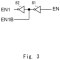
- the enable signal EN1 and the enable signal EN1B are generated based on the enable signal EN shown in Fig. 1 . More specifically, as shown in Fig. 3 , an inverter 81 and an inverter 82 output an enable signal EN1B and an enable signal EN1 with polarities different from each other, respectively.
- the enable signal EN1B is a signal obtained by inverting the enable signal EN once.
- the enable signal EN1 is a signal obtained by inverting the enable signal EN twice. Therefore, the enable signal EN1B is a signal obtained by inverting the enable signal EN1.
- the NOR circuit 111 and the NAND circuit 112 operate.
- the level of the enable signal EN1 is low, the NOR circuit 111 and the NAND circuit 112 stop operating.
- the comparator element 31 stops operating.
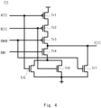
- NOR circuit 111 is a CMOS (complementary metal-oxide-semiconductor) circuit and includes 7 transistors Tr1 to Tr7.
- the transistors Tr1 to Tr3 are p-type MOS transistors.
- the transistors Tr4 to Tr7 are n-type MOS transistors.
- the transistors Tr1 to Tr4 are connected in series. Specifically, the transistors Tr1, Tr2, Tr3 and Tr4 are arranged from the power supply potential side to the ground side. The transistors Tr5 and Tr6 are connected in parallel between transistor Tr4 and the ground. An output signal C [1] is output from an output node between the transistors Tr3 and Tr4. In addition, the transistor Tr7 is arranged between the output node, which is located between the transistors Tr3 and Tr4, and the ground.
- the latch output A [1] is input to the gate of the transistor Tr1 and the gate of the transistor Tr5.
- the counter output B [1] is input to the gate of the transistor Tr2 and the gate of the transistor Tr6.
- the enable signal EN1 is input to the gate of the transistor Tr3 and the gate of the transistor Tr7.
- the enable signal EN1B is input to the gate of the transistor Tr4.
- the NOR circuit 111 operates normally. That is, the output signal C [1] is the negative logical sum of the latch output A [1] and the counter output B [1]. The output signal C [1] is input to the inverter 113 in Fig. 2 .
- the transistor Tr3 and the transistor Tr4 are turned off and the transistor Tr7 is turned on.
- the NOR circuit 111 does not function and the level of the output signal C [1] becomes low.
- the NOR circuit 111 prevents an unnecessary switching operation. Therefore, the current flowing from the power supply potential to the ground can be reduced.
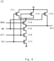
- Fig 5 shows the circuit configuration of the NAND circuit 112.
- the NAND circuit 112 is a CMOS circuit and has 7 transistors Tr 11 to Tr 17.
- the transistors Tr 11 to Tr 14 are p-type MOS transistors.
- the transistors Tr 15 to Tr 17 are n-type MOS transistors.
- the transistors Tr 14 to Tr 17 are connected in series. Specifically, the transistors Tr 17, Tr 16, Tr 15, and Tr 14 are arranged from the ground to the power supply potential. The transistors Tr 11 and Tr 12 are connected in parallel between the transistor Tr 14 and the power supply potential. An output signal D [1] is output from an output node between the transistor Tr 14 and the transistor Tr 15. In addition, the transistor Tr 13 is arranged between the output node, which is located between the transistors Tr 14 and Tr 15, and the power supply potential.
- the latch output A is input to the gate of the transistor Tr 12 and the gate of the transistor Tr 16.
- the counter output B is input to the gate of the transistor Tr 11 and the gate of the transistor Tr 17.
- the enable signal EN1 is input to the gate of the transistor Tr 13 and the gate of the transistor Tr 15.
- the enable signal EN1B is input to the gate of the transistor Tr 14.
- the NAND circuit 112 operates normally.
- the output signal D [1] becomes the negative logical sum of the latch output A [1] and the counter output B [1].
- the output signal D [1] is input to the NAND circuit 114 in Fig. 2 .
- the transistor Tr 14 and transistor Tr 15 are turned off and the transistor Tr 13 is turned on. Therefore, the NAND circuit 112 does not function, and the level of the output signal D [1] becomes high. The transistor Tr 14 and transistor Tr 15 are turned off. The NAND circuit 112 prevent an unnecessary switching operation. Therefore, the current flowing from the power supply potential to the ground can be reduced.
- the operation of the one bit comparator 110 is stopped by the enable signals EN1 and EN1B.
- the level of the enable signal EN1 is low, the value of the output signal C [1] becomes “0" and the value of the output signal D [1] becomes "1". That is, the output of the NOR circuit 111 and the output of the NAND circuit 112 are constant regardless of the values of the latch output A [1] and the counter output B [1].
- each of the 10 one bit comparators 110 includes the NOR circuit 111 shown in Fig. 4 and the NAND circuit 112 shown in Fig. 5 .
- the level of the enable signal EN1 is low, the level of the matching signal Z output from the comparator circuit 30 becomes low. Therefore, the matching signal Z becomes a positive pulse signal the level of which becomes high when the latch output A matches the counter output B.
- the output signal OUT from FF circuit 33 becomes the enable signal EN that stops the operation of comparator element 31.
- the comparator circuit 30 has a self-gating function that stops the switching operation by the enable signal EN generated by the FF circuit 33.
- the comparator circuit 30 can stop the comparator element 31 at an appropriate time. After the comparator element 31 outputs the positive pulse, it stops operating. Thus, the power consumption can be reduced.
- the switching operation in the comparator element 31 can be prevented. Therefore, the noise caused by the switching operation can be suppressed, thereby improving reliability.
- Fig. 6 shows the driver including the comparator circuit 30 of the comparative example. Note that the basic operation of the latch circuit 10, the counter 20, and the comparator element 31 is similar to that described with reference to Fig. 1 , so a detailed explanation is omitted. For example, comparator element 31 outputs the matching signal Z indicating that the latch output A matches the counter output B. The matching signal Z is a positive pulse.
- the comparator circuit 30 shown in Fig. 6 the output signal from FF circuit 33 is not used as the enable signal. Therefore, even after the latch output A matches the counter output B, the comparator element 31 performs the comparison operation. Thus, the comparator element 31 shown in Fig. 6 consumes more power than that of the comparator shown in Fig. 1 .
- the comparator element 31 stops operating in response to the enable signal EN from the comparator circuit 30. Therefore, the power consumption in the comparator circuit 30 shown in Fig. 1 can be reduced as compared to that of the comparator 30 shown in Fig. 6 .
- the comparator circuit 30 and the driver 100 can reduce the power consumption of a liquid crystal display device.
- LCOS Liquid Crystal On-Silicon
- the configuration of a liquid crystal display device 200 in which the comparator circuit 30 is applied to the driver will be described with reference to Fig. 7 .
- the liquid crystal display device 200 is an LCOS display.
- Fig. 7 is a block diagram showing the backplane of the LCOS display.
- the liquid crystal display device 200 includes a pixel display part 50, a vertical driver 2, and a horizontal driver 3.
- the horizontal driver 3 has the driver 100 shown in Fig. 1 .
- the horizontal driver 3 has m (m is an integer equal to or greater than 2) drivers 100, corresponding to the number of pixels for one line.
- the pixel display part 50 has a plurality of data lines 6, a plurality of gate lines 8 and a plurality of pixels 42.
- the plurality of the data lines 6 are arranged parallel to each other.
- the plurality of the gate lines 8 are arranged parallel to each other.
- the plurality of the data lines 6 are arranged to intersect with the plurality of the gate lines 8.
- the gate lines 8 are row scan lines.
- the liquid crystal display device 200 is includes two or more sets of the data lines 6 in a set of two data lines.
- the liquid crystal display device 200 inverts and drives the pixels 42 using one of the sets of the data lines 6.
- the data line 6 on the positive side is defined as a data line 6a
- the data line 6 on the negative side is defined as a data line 6b.
- switches 1 and video signal lines 5 the polarity is similarly respectively identified by defining a switch 1a, a switch 1b, a video signal line 5a and a video signal line5b.
- two systems including the data lines 6, the switches 1 and the video signal lines 5 are provided.
- the pixels 42 are located at the intersections of the data lines 6 and the gate lines 8.
- the pixels 42 are arranged in a matrix.
- Each pixel 42 is driven by one set of the two data lines 6 and one of the gate line 8.
- the pixels 42 are arranged in a matrix of n rows by m columns.
- Each of m and n is an integer equal to or greater than 2.
- Each of the pixels 42 includes a pixel driver and a pixel electrode to drive liquid crystals.
- the vertical driver 2 performs vertical drive to select the gate lines 8 for each horizontal scanning period.
- the vertical driver 2 supplies scanning signals to the gate lines 8. That is, the vertical driver 2 supplies the scanning signals so that the first row to n-th row of gate lines 8 are sequentially selected. This sequentially selects the pixels 42 for each row. All gate lines 8 are selected within one vertical scanning period. The pixels 42 in a selected row can be written by the video signal.
- the horizontal driver 3 performs horizontal driving to drive the switches 1 within a horizontal scanning period. In this way, the video signals are supplied to the plurality of the data lines 6.
- each set of the two data lines 6a and 6b is connected to the pixels 42 as a pair.
- the two data lines 6a and 6b are commonly connected to each of the pixels 42 in a row.
- the data line 6a is connected to the video signal line 5a via the switch 1a.
- the data line 6b is connected to the video signal line 5b via the switch 1b.
- a video signal RAMP+ on the positive side is supplied to the video signal line 5a.
- a video signal RAMP- on the negative side is supplied to the video signal line 5b.
- the horizontal driver 3 controls the switches 1a and 1b.
- one data line 6a of the set of the data line 6a and 6b is supplied with the video signal RAMP+ on the positive polarity
- the other data line 6b is supplied with the video signal RAMP- on the negative polarity.
- the video signal RAMP+ on the positive polarity becomes a positive voltage with respect to the common potential of the common electrode line
- the video signal RAMP- on the negative polarity becomes a negative voltage with respect to the common potential of the common electrode line.
- the horizontal driver 3 can supply the video signal RAMP+ on the positive polarity and the video signal RAMP- on the negative polarity to the pixels 42 in the selected row.
- the horizontal driver 3 turns each switch 1 on and off multiple times within the horizontal scanning period.
- the video signal RAMP+ on the positive polarity and the video signal RAMP-on the negative polarity are alternately supplied to the pixels 42.
- the horizontal driver 3 includes a latch circuit 310, a counter 320, a comparator circuit 330, a shift register 360 and buffers 370.
- the latch circuit 310 corresponds to the latch circuit 10 in Fig. 1 . That is, the latch circuit 310 has m columns of the latch circuits 10.
- the latch circuit 310 holds image data DATA of the pixels 42 in columns 1 to m.
- the comparator circuit 330 corresponds to the comparator circuit 30 in Fig. 1 . That is, the comparator circuit 330 has m columns of the comparator circuit 30.
- the output signal OUT from the comparator circuit 30 shown in Fig. 1 controls switch 1.
- the counter 320 corresponds to the counter 20 in Fig. 1 . Therefore, the counter 320 performs a counting operation according to the counter clock signal CNT_CLOCK.
- the shift register 360 sequentially transmits m columns of image data DATA according to the horizontal clock HCLOCK.
- the shift register 360 holds m columns of the image data DATA
- the shift register 360 outputs the image data DATA to the latch circuit 310.
- the latch circuit 310 stores the image data DATA of each column in response to the latch signal LATCH.
- the comparator circuit 330 compares the latch output A with the counter output B, as shown in Fig. 1 .
- the comparator circuit 330 controls a pair of switches 1a and 1b.
- the pair of switches 1a and 1b opens and closes in response to the output signal of the comparator circuit 330. Initially, the video signal is not supplied to the pixels 42 because all the pairs of the switches 1 are closed.
- the switch 1 which corresponds to video signal is opened.
- the video signal RAMP+ on the positive polarity and a video signal RAMP- on the negative polarity are alternately applied to the pixels 42.
- the liquid crystal display device 200 can perform gradation display according to the image data DATA.
- the buffers 370 buffer various signals output from an external controller.
- the buffers 370 are used to drive loads that are heavy due to the large number of rows in the pixel display part 50.
- a horizontal clock signal HCLOCK is input to the shift register 360 via the buffer 370.
- the latch signal LATCH is input to the latch circuit 310 via the buffer 370.
- the counter output from the counter 320 is input to the comparator circuit 330 via the buffer 370.
- the comparator circuit 330 includes the comparator circuit 30 shown in Fig. 1 .
- a buffer for the comparator clock signal input into the comparator circuit 330 can be omitted.
- the number of buffers can be reduced in accordance with the number of columns, and thus it is possible to reduce power consumption. Furthermore, since timing errors can be suppressed, reliability can be improved.
Landscapes
- Physics & Mathematics (AREA)
- Engineering & Computer Science (AREA)
- Computer Hardware Design (AREA)
- Computing Systems (AREA)
- General Engineering & Computer Science (AREA)
- Mathematical Physics (AREA)
- General Physics & Mathematics (AREA)
- Theoretical Computer Science (AREA)
- Nonlinear Science (AREA)
- Chemical & Material Sciences (AREA)
- Crystallography & Structural Chemistry (AREA)
- Liquid Crystal Display Device Control (AREA)
- Control Of Indicators Other Than Cathode Ray Tubes (AREA)
- Manipulation Of Pulses (AREA)
Abstract
Description
- This disclosure relates to a comparator circuit and a driver.
- In
Fig. 2 ofPatent Literature 1, a comparator compares the counter output with pixel value of the digital image data. The comparator outputs a matching pulse indicating the both data are matched to the D-type flip-flop circuit. Then, the positive and negative polarity switches are switched in conjunction with the output of the D-type flip-flop. - Patent Literature 1:
Japanese Unexamined Patent Application Publication No. 2013 -105166 - In
Patent literature 1, the comparator performs a comparison operation to compare the counter output with the digital image data even after the counter output matches the digital image data. In other words, even after the comparator outputs the matching pulse, the switching operation continues. Therefore, there is a problem when the power consumption in the comparator becomes large. - This disclosure is made in view of the above as described above, and an object of the present invention is to provide a comparator circuit and a driver with a low power consumption.
- A comparator circuit according to this embodiment including; a comparator element configured to output a matching signal indicating whether or not a value of a first input signal matches a value of a second input signal; a flip-flop circuit configured to hold a data of a data input terminal based on a comparator clock signal and configured to output an enable signal for stopping an operation of the comparator element; and an internal signal generation circuit configured to output an internal signal to the data input terminal based on the matching signal and an output signal output from the flip-flop circuit.
- According to the present disclosure, it is possible to provide a comparator circuit and a driver with a low power consumption.
-
-
Fig. 1 is a circuit diagram showing the configuration of the driver using the comparator circuit; -
Fig. 2 is a circuit diagram showing the configuration of comparator element; -
Fig. 3 is a circuit diagram showing the polarity of the enable signals EN1 and EN1B; -
Fig, 4 is a circuit diagram of theNOR circuit 111; -
Fig. 5 is a circuit diagram of theNAND circuit 112; -
Fig. 6 is a circuit diagram showing the configuration of the comparator circuit in a comparative example; and -
Fig. 7 shows a configuration of a liquid crystal display device using a driver. - Hereafter, a specific embodiment to which the present invention is applied will be described in detail with reference to the drawings. However, this disclosure is not limited to the following examples. In addition, the following descriptions and drawings have been simplified, as appropriate, for clarity.
- The comparator circuit according to the present embodiment and the driver using it are described below.
Fig. 1 is a circuit diagram showing adriver 100 with acomparator circuit 30. Specifically, the driver shown inFig. 1 is a horizontal driver for driving one row of pixels in a liquid crystal display device. - The
driver 100 includes alatch circuit 10, acounter 20 and thecomparator circuit 30. Here, 10-bit image data DATA are input to thedriver 100. That is, one pixel is represented in 1,024 greyscales (= 10 bits). Of course, the number of bits of image data is not limited to the above values. - A latch signal LATCH and the image data DATA are input to the
latch circuit 10. Thelatch circuit 10 latches the 10-bit image data DATA in response to the latch signal LATCH. Thelatch circuit 10 outputs the latched image data DATA to thecomparator circuit 30 in parallel. The image data DATA output from thelatch circuit 10 is defined as the latch output A. The latch output A is 10-bit parallel data. InFig. 2 , the value of the latch output A is defined as α. - A counter clock signal CNT_CLOCK and a counter reset signal CNT_RST are input to the
counter 20. Thecounter 20 performs a counting operation in synchronization with the counter clock signal CNT_CLOCK. For example, thecounter 20 counts up the count value at the clock frequency of the counter clock signal CNT_CLOCK. Thecounter 20 outputs the count value generated by the counting operation to thecomparator circuit 30. - The
counter 20 resets the count value to the initial value in response to the counter reset signal CNT_RST. The counter reset signal CNT_RST corresponds to the horizontal scanning frequency. The output ofcounter 20 is 10-bits. Thus, thecounter 20 increments the count value by one from 0 to 1023. Thecounter 20 outputs a 10-bit count value to thecomparator circuit 30. The count value output from thecounter 20 is defined as the counter output B. The counter output B is 10-bit parallel data. - The
comparator circuit 30 includes acomparator element 31, a FF (flip-flop)circuit 33 and an internalsignal generation circuit 36. The internalsignal generation circuit 36 includes aninverter 34 and aOR circuit 35. - The
comparator element 31 compares the latch output A with the counter output B. Thecomparator element 31 generates a matching signal Z indicating that the latch output A matches the counter output B. Thecomparator element 31 outputs the matching signal Z to theOR circuit 35. The latch output A and the counter output B are each 10-bits of parallel data, respectively. Thecomparator element 31 compares each bit of the latch output A with each corresponding bit of the counter output B. Thecomparator element 31 determines that the latch output A matches the counter output B when all the bits of the latch output A respectively coincide with those of the counter output B. - When the latch output A matches the counter output B, the
comparator element 31 asserts the matching signal Z. When the latch output A does not match the counter output B, thecomparator element 31 deasserts the matching signal Z, and therefore the matching signal Z becomes a positive pulse signal which becomes a high-level signal when the latch output A matches the counter output B. - The internal
signal generation circuit 36 generates an internal signal Z1 based on the output signals OUT from theFF circuit 33 and the matching signal Z. The internalsignal generation circuit 36 outputs the internal signal Z1 to theFF circuit 33. - The
FF circuit 33 is a D-type flip-flop circuit. TheFF circuit 33 has a data input terminal D, a clock input terminal CK, a non-inverted output terminal Q, and an inverted output terminal QB. The output of the internalsignal generation circuit 36 is connected to a data input terminal D. The internal signal Z1 from theOR circuit 35 is input to the data input terminal D. A comparator clock signal CMP_CLOCK is input to the clock input terminal CK from an external circuit. TheFF circuit 33 samples and holds the data value of the data input terminal D according to the comparator clock signal CMP_CLOCK. TheFF circuit 33 holds a value of 1-bit. - The
FF circuit 33 outputs a non-inverted output signal corresponding to the held value from the non-inverted output terminal Q. TheFF circuit 33 outputs the inverted output signal obtained by inverting the non-inverted output signal from the inverted output terminal QB. The inverted output signal becomes the output signal OUT from thecomparator circuit 30. When the value of the input data held by theFF circuit 33 is 1, the level of the non-inverted output signal becomes high while the level of the inverted output signal becomes low. When the value of the input data held by theFF circuit 33 is 0, the level of the non-inverted output signal becomes low while the level of the inverted output signal becomes high. - The output signal OUT of the
FF circuit 33 is input to theFF circuit 33 via aninverter 34. Theinverter 34 inverts the output signal OUT from theFF circuit 33 and outputs it to theOR circuit 35. The ORcircuit 35 outputs a logical sum of the output from theinverter 34 and the matching signal Z as the internal signal Z1. The ORcircuit 35 outputs the internal signal Z1 to the data input terminal D ofFF circuit 33. - A comparator reset signal CMP_RST is input to the
FF circuit 33. TheFF circuit 33 resets the holding data in response to the comparator reset signal CMP RST. As a result, the data value held in theFF circuit 33 becomes 0. When theFF circuit 33 is reset by the comparator reset signal CMP_RST, the level of the inverted output signal becomes high while the level of the non-inverted output signal becomes low. - After the
FF circuit 33 is reset by the comparator reset signal CMP_RST, theFF circuit 33 samples the value of the internal signal Z1 in response to the internal signal Z1. Therefore, the output signal OUT output from the inverted output terminal QB becomes a negative step signal when the level of the internal signal Z1 is high - Furthermore, the output signal OUT from the inverted output terminal of
FF circuit 33 becomes an enable signal EN to control thecomparator element 31. That is, the output signal OUT is input to thecomparator element 31 as the enable signal EN. Thecomparator element 31 stops operating in response to the enable signal EN. Specifically, when the level of the enable signal is high, thecomparator element 31 performs the comparison operation as a usual. When the level of the enable signal is low, thecomparator element 31 stops the comparison operation. When the level of the enable signal EN is high, thecomparator element 31 compares the latch output A with the counter output B. When the level of the enable signal EN is low, the level of the matching signal Z is fixed so as to be low without thecomparator element 31 comparing the latch output A with the counter output B. - Thus, the
comparator element 31 stops operating in response to the output signal OUT from theFF circuit 33. That is, the output signal OUT, which is a negative step signal, stops thecomparator element 31. Specifically, after thecomparator element 31 outputs a positive pulse signal as the matching signal Z, thecomparator element 31 stops operating. This prevents switching operation from occurring in thecomparator element 31, thus reducing a power consumption. -
Fig. 2 is a circuit diagram showing an example of the configuration of thecomparator element 31. As described above, thecomparator element 31 compares 10 bits of data to each other. For the latch output A and the counter output B, the 1st bit data is defined as the latch output A [1] and the counter output B [1], respectively, and the 10th bit data is defined as the latch output A [10] and the counter output B [10]. - The
comparator element 31 includes a plurality of onebit comparators 110, aNAND circuit 150, and aninverter 160. Thecomparator element 31 has 10 onebit comparators 110 for comparing 10 bits of data to each other. The number of onebit comparators 110 is equal to the number of bits of the latch output A, that is, the number corresponding to the number of gradation bits. The respective circuit configurations of the onebit comparators 110 are the same as each other. The 2nd to 9th onebit comparators 110 are omitted inFig. 2 . In the following description, we mainly describe the onebit comparator 110 that compares the latch output A [1] with the counter output B [1]. - The one
bit comparator 110 includes a NORcircuit 111, aNAND circuit 112, aninverter 113, and aNAND circuit 114. The first bit latch output A [1] and the first bit counter output B [1] are input to the NORcircuit 111. The NORcircuit 111 outputs the NOR (a negative logical sum) of the latch output A [1] and the counter output B [1] to theinverter 113. Theinverter 113 inverts the output of the NORcircuit 111 and outputs it to theNAND circuit 114. - The first bit latch output A [1] and the counter output B [1] are input to the
NAND circuit 112. TheNAND circuit 112 outputs the NAND (a negative logical product) of the latch output A [1] and the counter output B [1] to theNAND circuit 114. The output of theNAND circuit 112 and the output of theinverter 113 are input to theNAND circuit 114. TheNAND circuit 114 outputs the NAND (a negative logical sum) of the output of theNAND circuit 112 and the output of theinverter 113 to theNAND circuit 150 as an output signal OUT [1]. When the value of the latch output A [1] matches the value of the counter output B [1], the level of the output of theNAND circuit 150 becomes high. - As described above, the
comparator element 31 includes the 10 one bit comparators 110. The outputs of the 10 onebit comparators 110 are input to theNAND circuit 150. For example, the 10th onebit comparator 110 outputs the negative logical product of theNAND circuit 114 to theNAND circuit 150 as an output signal OUT [10]. - The
NAND circuit 150 outputs the negative logical product of 10 bits of output signals OUT [1] to OUT [10] to theinverter 160. Theinverter 160 inverts the output ofNAND circuit 150. The signal output from theinverter 160 becomes the matching signal Z. When the levels of the output signal OUT [1] to the output signal OUT [10] are high, the level of the matching signal Z becomes high. The matching signal Z is asserted when the bit values of latch outputs A [1] to A [10] respectively match bit values of the counter outputs B [1] to B [10]. The matching signal Z is deasserted when at least one bit value of latch outputs A [1] to A [10] is different from a value of the corresponding bit of the counter outputs B [1] to B [10]. - Furthermore, enable signals EN1 and EN1B are input to the NOR
circuit 111 and theNAND circuit 112. The enable signal EN1 and the enable signal EN1B are generated based on the enable signal EN shown inFig. 1 . More specifically, as shown inFig. 3 , aninverter 81 and aninverter 82 output an enable signal EN1B and an enable signal EN1 with polarities different from each other, respectively. The enable signal EN1B is a signal obtained by inverting the enable signal EN once. The enable signal EN1 is a signal obtained by inverting the enable signal EN twice. Therefore, the enable signal EN1B is a signal obtained by inverting the enable signal EN1. - When the level of the enable signal EN1 is high, the NOR
circuit 111 and theNAND circuit 112 operate. When the level of the enable signal EN1 is low, the NORcircuit 111 and theNAND circuit 112 stop operating. Thus, if the level of the enable signal EN is low, thecomparator element 31 stops operating. -
Fig. 4 shows the circuit configuration of the NORcircuit 111. NORcircuit 111 is a CMOS (complementary metal-oxide-semiconductor) circuit and includes 7 transistors Tr1 to Tr7. The transistors Tr1 to Tr3 are p-type MOS transistors. The transistors Tr4 to Tr7 are n-type MOS transistors. - The transistors Tr1 to Tr4 are connected in series. Specifically, the transistors Tr1, Tr2, Tr3 and Tr4 are arranged from the power supply potential side to the ground side. The transistors Tr5 and Tr6 are connected in parallel between transistor Tr4 and the ground. An output signal C [1] is output from an output node between the transistors Tr3 and Tr4. In addition, the transistor Tr7 is arranged between the output node, which is located between the transistors Tr3 and Tr4, and the ground.
- The latch output A [1] is input to the gate of the transistor Tr1 and the gate of the transistor Tr5. The counter output B [1] is input to the gate of the transistor Tr2 and the gate of the transistor Tr6. The enable signal EN1 is input to the gate of the transistor Tr3 and the gate of the transistor Tr7. The enable signal EN1B is input to the gate of the transistor Tr4.
- Therefore, when the level of the enable signal EN1 is high, the NOR
circuit 111 operates normally. That is, the output signal C [1] is the negative logical sum of the latch output A [1] and the counter output B [1]. The output signal C [1] is input to theinverter 113 inFig. 2 . - When the level of the enable signal EN1 is low, the transistor Tr3 and the transistor Tr4 are turned off and the transistor Tr7 is turned on. The NOR
circuit 111 does not function and the level of the output signal C [1] becomes low. The NORcircuit 111 prevents an unnecessary switching operation. Therefore, the current flowing from the power supply potential to the ground can be reduced. -
Fig 5 shows the circuit configuration of theNAND circuit 112. TheNAND circuit 112 is a CMOS circuit and has 7 transistors Tr 11 to Tr 17. The transistors Tr 11 to Tr 14 are p-type MOS transistors. Thetransistors Tr 15 to Tr 17 are n-type MOS transistors. - The transistors Tr 14 to Tr 17 are connected in series. Specifically, the transistors Tr 17,
Tr 16,Tr 15, and Tr 14 are arranged from the ground to the power supply potential. The transistors Tr 11 andTr 12 are connected in parallel between the transistor Tr 14 and the power supply potential. An output signal D [1] is output from an output node between the transistor Tr 14 and thetransistor Tr 15. In addition, thetransistor Tr 13 is arranged between the output node, which is located between the transistors Tr 14 andTr 15, and the power supply potential. - The latch output A is input to the gate of the
transistor Tr 12 and the gate of thetransistor Tr 16. The counter output B is input to the gate of the transistor Tr 11 and the gate of the transistor Tr 17. The enable signal EN1 is input to the gate of thetransistor Tr 13 and the gate of thetransistor Tr 15. The enable signal EN1B is input to the gate of the transistor Tr 14. - Therefore, when the level of the enable signal EN1 is high, the
NAND circuit 112 operates normally. The output signal D [1] becomes the negative logical sum of the latch output A [1] and the counter output B [1]. The output signal D [1] is input to theNAND circuit 114 inFig. 2 . - When the level of the enable signal EN1 is low, the transistor Tr 14 and
transistor Tr 15 are turned off and thetransistor Tr 13 is turned on. Therefore, theNAND circuit 112 does not function, and the level of the output signal D [1] becomes high. The transistor Tr 14 andtransistor Tr 15 are turned off. TheNAND circuit 112 prevent an unnecessary switching operation. Therefore, the current flowing from the power supply potential to the ground can be reduced. - Thus, the operation of the one
bit comparator 110 is stopped by the enable signals EN1 and EN1B. When the level of the enable signal EN1 is low, the value of the output signal C [1] becomes "0" and the value of the output signal D [1] becomes "1". That is, the output of the NORcircuit 111 and the output of theNAND circuit 112 are constant regardless of the values of the latch output A [1] and the counter output B [1]. - When the level of the enable signal EN1 is low, the value of the output signal OUT [1] of the
NAND circuit 114 shown inFig. 2 becomes "0". Each of the 10 onebit comparators 110 includes the NORcircuit 111 shown inFig. 4 and theNAND circuit 112 shown inFig. 5 . When the level of the enable signal EN1 is low, the level of the matching signal Z output from thecomparator circuit 30 becomes low. Therefore, the matching signal Z becomes a positive pulse signal the level of which becomes high when the latch output A matches the counter output B. - As described above, the output signal OUT from
FF circuit 33 becomes the enable signal EN that stops the operation ofcomparator element 31. Thecomparator circuit 30 has a self-gating function that stops the switching operation by the enable signal EN generated by theFF circuit 33. Thecomparator circuit 30 can stop thecomparator element 31 at an appropriate time. After thecomparator element 31 outputs the positive pulse, it stops operating. Thus, the power consumption can be reduced. - Furthermore, the switching operation in the
comparator element 31 can be prevented. Therefore, the noise caused by the switching operation can be suppressed, thereby improving reliability. -
Fig. 6 shows the driver including thecomparator circuit 30 of the comparative example. Note that the basic operation of thelatch circuit 10, thecounter 20, and thecomparator element 31 is similar to that described with reference toFig. 1 , so a detailed explanation is omitted. For example,comparator element 31 outputs the matching signal Z indicating that the latch output A matches the counter output B. The matching signal Z is a positive pulse. - In the
comparator circuit 30 shown inFig. 6 , the output signal fromFF circuit 33 is not used as the enable signal. Therefore, even after the latch output A matches the counter output B, thecomparator element 31 performs the comparison operation. Thus, thecomparator element 31 shown inFig. 6 consumes more power than that of the comparator shown inFig. 1 . - On the other hand, in the
comparator circuit 30 shown inFig. 1 , thecomparator element 31 stops operating in response to the enable signal EN from thecomparator circuit 30. Therefore, the power consumption in thecomparator circuit 30 shown inFig. 1 can be reduced as compared to that of thecomparator 30 shown inFig. 6 . - The
comparator circuit 30 and thedriver 100 according to this embodiment can reduce the power consumption of a liquid crystal display device. When thedriver 100 is applied to a WUXGA Liquid Crystal On-Silicon (LCOS) device with a frame rate of 120 Hz, the power consumption of the device can be reduced from 1188 mW to 1126 mW. That means an 5.3% (= 62 mW) reduction in power consumption. - The configuration of a liquid
crystal display device 200 in which thecomparator circuit 30 is applied to the driver will be described with reference toFig. 7 . The liquidcrystal display device 200 is an LCOS display.Fig. 7 is a block diagram showing the backplane of the LCOS display. - The liquid
crystal display device 200 includes apixel display part 50, avertical driver 2, and ahorizontal driver 3. Thehorizontal driver 3 has thedriver 100 shown inFig. 1 . Specifically, thehorizontal driver 3 has m (m is an integer equal to or greater than 2)drivers 100, corresponding to the number of pixels for one line. - The
pixel display part 50 has a plurality ofdata lines 6, a plurality ofgate lines 8 and a plurality ofpixels 42. The plurality of thedata lines 6 are arranged parallel to each other. The plurality of thegate lines 8 are arranged parallel to each other. The plurality of thedata lines 6 are arranged to intersect with the plurality of the gate lines 8. The gate lines 8 are row scan lines. - The liquid
crystal display device 200 is includes two or more sets of thedata lines 6 in a set of two data lines. The liquidcrystal display device 200 inverts and drives thepixels 42 using one of the sets of the data lines 6. Hereafter, regarding the sets of thedata lines 6, thedata line 6 on the positive side is defined as adata line 6a, and thedata line 6 on the negative side is defined as adata line 6b. Forswitches 1 andvideo signal lines 5, the polarity is similarly respectively identified by defining aswitch 1a, aswitch 1b, avideo signal line 5a and a video signal line5b. To reverse the polarity, two systems including thedata lines 6, theswitches 1 and thevideo signal lines 5 are provided. - The
pixels 42 are located at the intersections of thedata lines 6 and the gate lines 8. Thepixels 42 are arranged in a matrix. Eachpixel 42 is driven by one set of the twodata lines 6 and one of thegate line 8. For example, when there aren gate lines 8 and 2m data lines, thepixels 42 are arranged in a matrix of n rows by m columns. Each of m and n is an integer equal to or greater than 2. Each of thepixels 42 includes a pixel driver and a pixel electrode to drive liquid crystals. - The
vertical driver 2 performs vertical drive to select thegate lines 8 for each horizontal scanning period. Thevertical driver 2 supplies scanning signals to the gate lines 8. That is, thevertical driver 2 supplies the scanning signals so that the first row to n-th row ofgate lines 8 are sequentially selected. This sequentially selects thepixels 42 for each row. Allgate lines 8 are selected within one vertical scanning period. Thepixels 42 in a selected row can be written by the video signal. - The
horizontal driver 3 performs horizontal driving to drive theswitches 1 within a horizontal scanning period. In this way, the video signals are supplied to the plurality of the data lines 6. As described above, each set of the twodata lines pixels 42 as a pair. Thus, the twodata lines pixels 42 in a row. - The
data line 6a is connected to thevideo signal line 5a via theswitch 1a. Thedata line 6b is connected to thevideo signal line 5b via theswitch 1b. A video signal RAMP+ on the positive side is supplied to thevideo signal line 5a. A video signal RAMP- on the negative side is supplied to thevideo signal line 5b. Thehorizontal driver 3 controls theswitches - Thus, one
data line 6a of the set of thedata line other data line 6b is supplied with the video signal RAMP- on the negative polarity. The video signal RAMP+ on the positive polarity becomes a positive voltage with respect to the common potential of the common electrode line, and the video signal RAMP- on the negative polarity becomes a negative voltage with respect to the common potential of the common electrode line. Thehorizontal driver 3 can supply the video signal RAMP+ on the positive polarity and the video signal RAMP- on the negative polarity to thepixels 42 in the selected row. Thehorizontal driver 3 turns eachswitch 1 on and off multiple times within the horizontal scanning period. Thus, the video signal RAMP+ on the positive polarity and the video signal RAMP-on the negative polarity are alternately supplied to thepixels 42. - Specifically, the
horizontal driver 3 includes alatch circuit 310, acounter 320, acomparator circuit 330, ashift register 360 and buffers 370. Thelatch circuit 310 corresponds to thelatch circuit 10 inFig. 1 . That is, thelatch circuit 310 has m columns of thelatch circuits 10. Thelatch circuit 310 holds image data DATA of thepixels 42 incolumns 1 to m. - The
comparator circuit 330 corresponds to thecomparator circuit 30 inFig. 1 . That is, thecomparator circuit 330 has m columns of thecomparator circuit 30. The output signal OUT from thecomparator circuit 30 shown inFig. 1 controls switch 1. Thecounter 320 corresponds to thecounter 20 inFig. 1 . Therefore, thecounter 320 performs a counting operation according to the counter clock signal CNT_CLOCK. - The
shift register 360 sequentially transmits m columns of image data DATA according to the horizontal clock HCLOCK. When theshift register 360 holds m columns of the image data DATA, theshift register 360 outputs the image data DATA to thelatch circuit 310. Thelatch circuit 310 stores the image data DATA of each column in response to the latch signal LATCH. - The
comparator circuit 330 compares the latch output A with the counter output B, as shown inFig. 1 . Thecomparator circuit 330 controls a pair ofswitches switches comparator circuit 330. Initially, the video signal is not supplied to thepixels 42 because all the pairs of theswitches 1 are closed. When the output signal of thecomparator circuit 330 is asserted, theswitch 1 which corresponds to video signal is opened. Thus, the video signal RAMP+ on the positive polarity and a video signal RAMP- on the negative polarity are alternately applied to thepixels 42. The liquidcrystal display device 200 can perform gradation display according to the image data DATA. - The
buffers 370 buffer various signals output from an external controller. Thebuffers 370 are used to drive loads that are heavy due to the large number of rows in thepixel display part 50. For example, a horizontal clock signal HCLOCK is input to theshift register 360 via thebuffer 370. Similarly, the latch signal LATCH is input to thelatch circuit 310 via thebuffer 370. The counter output from thecounter 320 is input to thecomparator circuit 330 via thebuffer 370. - In this embodiment, the
comparator circuit 330 includes thecomparator circuit 30 shown inFig. 1 . Thus, a buffer for the comparator clock signal input into thecomparator circuit 330 can be omitted. In other words, the number of buffers can be reduced in accordance with the number of columns, and thus it is possible to reduce power consumption. Furthermore, since timing errors can be suppressed, reliability can be improved. - As described above, the invention made by the inventor has been specifically explained based on the embodiment, but the invention is not limited to the above embodiment, and it goes without saying that various modifications can be made without departing from the gist of the invention.
- This application is based upon and claims the benefit of priority from
Japanese patent application No. 2021-087342, filed on May 25, 2021 -
- 1 SWITCH
- 2 VERTICAL DRIVER
- 3 HORIZONTAL DRIVER
- 6 DATA LINE
- 8 GATE LINE
- 42 PIXEL
- 50 PIXEL DISPLAY PART
- 100 DRIVER
- 10 LATCH CIRCUIT
- 20 COUNTER
- 30 COMPARATOR CIRCUIT
- 31 COMPARATOR ELEMENT
- 33 FF CIRCUIT
- 34 INVERTER
- 35 OR CIRCUIT
- 36 INTERNAL SIGNAL GENERATION CIRCUIT
- 200 LIQUID CRYSTAL DISPLAY DEVICE
- 310 LATCH CIRCUIT
- 320 COUNTER
- 330 COMPARATOR CIRCUIT
- 360 SHIFT REGISTER
- 370 BUFFER
Claims (5)
- A comparator circuit: comprising:a comparator element configured to output a matching signal indicating whether or not a value of a first input signal matches a value of a second input signal;a flip-flop circuit configured to hold a data of a data input terminal based on a comparator clock signal and configured to output an enable signal for stopping an operation of the comparator element; andan internal signal generation circuit configured to output an internal signal to the data input terminal based on the matching signal and an output signal output from the flip-flop circuit.
- The comparator circuit according to claim 1, wherein an inverted output signal output from an inverted output terminal of the flip-flop circuit is the enable signal.
- The comparator circuit according to claim 2, wherein the internal signal generation circuit comprises:an inverter to which the inverted output signal is input; andan OR circuit configured to output a logical sum of a signal output from the inverter and the matching signal.
- The comparator circuit according to any one of claims 1 to 3, wherein the comparator element comprises a PMOS Transistor and a NMOS transistor connected in series between a power supply potential and a ground potential, and
wherein the PMOS transistor and the NMOS transistor operate in accordance with the enable signal. - A driver of a liquid crystal display device comprising:a comparator circuit according to any one of claims 1 to 4;a latch circuit configured to hold pixel data and output the pixel data to the comparator circuit as the first input signal; anda counter configured to perform a count operation in accordance with a counter clock signal and output a count value as the second input signal.
Applications Claiming Priority (2)
| Application Number | Priority Date | Filing Date | Title |
|---|---|---|---|
| JP2021087342A JP7676952B2 (en) | 2021-05-25 | 2021-05-25 | Comparator circuit and driver circuit |
| PCT/JP2022/006204 WO2022249584A1 (en) | 2021-05-25 | 2022-02-16 | Comparator circuit, and driver circuit |
Publications (2)
| Publication Number | Publication Date |
|---|---|
| EP4350994A1 true EP4350994A1 (en) | 2024-04-10 |
| EP4350994A4 EP4350994A4 (en) | 2024-08-07 |
Family
ID=84229812
Family Applications (1)
| Application Number | Title | Priority Date | Filing Date |
|---|---|---|---|
| EP22773374.8A Pending EP4350994A4 (en) | 2021-05-25 | 2022-02-16 | COMPARATOR CIRCUIT AND DRIVER CIRCUIT |
Country Status (5)
| Country | Link |
|---|---|
| US (1) | US11996841B2 (en) |
| EP (1) | EP4350994A4 (en) |
| JP (1) | JP7676952B2 (en) |
| CN (1) | CN115699578A (en) |
| WO (1) | WO2022249584A1 (en) |
Family Cites Families (11)
| Publication number | Priority date | Publication date | Assignee | Title |
|---|---|---|---|---|
| JPS52120665A (en) * | 1976-04-02 | 1977-10-11 | Gorou Kouda | Frequency divider using ic flippflop |
| JP3279812B2 (en) * | 1994-05-24 | 2002-04-30 | 三菱電機株式会社 | Runaway monitoring circuit of PLL control circuit |
| JP4289206B2 (en) * | 2004-04-26 | 2009-07-01 | ソニー株式会社 | Counter circuit |
| KR100573073B1 (en) * | 2004-07-29 | 2006-04-24 | 매그나칩 반도체 유한회사 | 2-bit binary comparator and binary comparator using the same |
| US7919991B1 (en) * | 2008-07-08 | 2011-04-05 | Netlogic Microsystems, Inc. | Comparator circuit |
| JP5407523B2 (en) * | 2009-04-24 | 2014-02-05 | ソニー株式会社 | Integrating AD converter, solid-state imaging device, and camera system |
| JP2011205393A (en) * | 2010-03-25 | 2011-10-13 | Riniaseru Design:Kk | Solid-state imaging apparatus, and method of driving the same |
| JP5786669B2 (en) * | 2011-11-17 | 2015-09-30 | 株式会社Jvcケンウッド | Liquid crystal display |
| JP2015115907A (en) * | 2013-12-16 | 2015-06-22 | ソニー株式会社 | Analog to digital converter |
| US10360846B2 (en) * | 2016-05-10 | 2019-07-23 | X-Celeprint Limited | Distributed pulse-width modulation system with multi-bit digital storage and output device |
| JP7370834B2 (en) | 2019-11-29 | 2023-10-30 | キヤノン株式会社 | Electronic equipment and control methods |
-
2021
- 2021-05-25 JP JP2021087342A patent/JP7676952B2/en active Active
-
2022
- 2022-02-16 CN CN202280003135.6A patent/CN115699578A/en active Pending
- 2022-02-16 EP EP22773374.8A patent/EP4350994A4/en active Pending
- 2022-02-16 WO PCT/JP2022/006204 patent/WO2022249584A1/en not_active Ceased
- 2022-09-28 US US17/955,190 patent/US11996841B2/en active Active
Also Published As
| Publication number | Publication date |
|---|---|
| JP2022180709A (en) | 2022-12-07 |
| US20230015972A1 (en) | 2023-01-19 |
| EP4350994A4 (en) | 2024-08-07 |
| WO2022249584A1 (en) | 2022-12-01 |
| US11996841B2 (en) | 2024-05-28 |
| CN115699578A (en) | 2023-02-03 |
| JP7676952B2 (en) | 2025-05-15 |
Similar Documents
| Publication | Publication Date | Title |
|---|---|---|
| JP5078533B2 (en) | Gate line drive circuit | |
| US10095058B2 (en) | Shift register and driving method thereof, gate driving device | |
| US7664218B2 (en) | Shift register and image display apparatus containing the same | |
| US10475409B2 (en) | Gate drive circuit, display panel, and driving method for the gate drive circuit | |
| CN101336447B (en) | Display apparatus and method for driving the same | |
| JP5496270B2 (en) | Gate line drive circuit | |
| US6989810B2 (en) | Liquid crystal display and data latch circuit | |
| US8791937B2 (en) | Over-drivable output buffer, source driver circuit having the same, and methods therefor | |
| US20070248204A1 (en) | Shift register circuit and image display apparatus equipped with the same | |
| US8922460B2 (en) | Level shift circuit, data driver, and display device | |
| US20170256223A1 (en) | Gate driver and liquid crytal display | |
| US7292218B2 (en) | Shift-register circuit | |
| US20120086686A1 (en) | Display driving circuit, display device and display driving method | |
| JP5207865B2 (en) | Shift register | |
| TWI663587B (en) | Common voltage generating circuit | |
| US11996841B2 (en) | Comparator circuit and driver | |
| US11984892B2 (en) | Comparator circuit and driver | |
| WO2013002191A1 (en) | Holding circuit, display drive circuit, display panel, and display device | |
| CN112289251A (en) | GOA circuit and display panel | |
| US10490155B2 (en) | Liquid crystal display device | |
| CN114743519B (en) | GOA circuit and display panel | |
| CN104299581B (en) | Display and grid drive circuit thereof | |
| JP2004127509A (en) | Shift register circuit and image display device | |
| TWM675078U (en) | Gate drive circuit and display panel | |
| JPH0612035A (en) | Display device |
Legal Events
| Date | Code | Title | Description |
|---|---|---|---|
| STAA | Information on the status of an ep patent application or granted ep patent |
Free format text: STATUS: UNKNOWN |
|
| STAA | Information on the status of an ep patent application or granted ep patent |
Free format text: STATUS: THE INTERNATIONAL PUBLICATION HAS BEEN MADE |
|
| PUAI | Public reference made under article 153(3) epc to a published international application that has entered the european phase |
Free format text: ORIGINAL CODE: 0009012 |
|
| STAA | Information on the status of an ep patent application or granted ep patent |
Free format text: STATUS: REQUEST FOR EXAMINATION WAS MADE |
|
| 17P | Request for examination filed |
Effective date: 20220929 |
|
| AK | Designated contracting states |
Kind code of ref document: A1 Designated state(s): AL AT BE BG CH CY CZ DE DK EE ES FI FR GB GR HR HU IE IS IT LI LT LU LV MC MK MT NL NO PL PT RO RS SE SI SK SM TR |
|
| A4 | Supplementary search report drawn up and despatched |
Effective date: 20240705 |
|
| RIC1 | Information provided on ipc code assigned before grant |
Ipc: H03K 5/19 20060101ALI20240701BHEP Ipc: G09G 3/36 20060101ALI20240701BHEP Ipc: G09G 3/20 20060101ALI20240701BHEP Ipc: H03K 3/037 20060101AFI20240701BHEP |
|
| DAV | Request for validation of the european patent (deleted) | ||
| DAX | Request for extension of the european patent (deleted) |