EP4336678A2 - Handstück mit einem mikrochiplaser - Google Patents
Handstück mit einem mikrochiplaser Download PDFInfo
- Publication number
- EP4336678A2 EP4336678A2 EP24152441.2A EP24152441A EP4336678A2 EP 4336678 A2 EP4336678 A2 EP 4336678A2 EP 24152441 A EP24152441 A EP 24152441A EP 4336678 A2 EP4336678 A2 EP 4336678A2
- Authority
- EP
- European Patent Office
- Prior art keywords
- laser
- handpiece
- microchip
- microchip laser
- skin
- Prior art date
- Legal status (The legal status is an assumption and is not a legal conclusion. Google has not performed a legal analysis and makes no representation as to the accuracy of the status listed.)
- Pending
Links
Images




Classifications
-
- H—ELECTRICITY
- H01—ELECTRIC ELEMENTS
- H01S—DEVICES USING THE PROCESS OF LIGHT AMPLIFICATION BY STIMULATED EMISSION OF RADIATION [LASER] TO AMPLIFY OR GENERATE LIGHT; DEVICES USING STIMULATED EMISSION OF ELECTROMAGNETIC RADIATION IN WAVE RANGES OTHER THAN OPTICAL
- H01S3/00—Lasers, i.e. devices using stimulated emission of electromagnetic radiation in the infrared, visible or ultraviolet wave range
- H01S3/05—Construction or shape of optical resonators; Accommodation of active medium therein; Shape of active medium
- H01S3/06—Construction or shape of active medium
- H01S3/0619—Coatings, e.g. AR, HR, passivation layer
- H01S3/0621—Coatings on the end-faces, e.g. input/output surfaces of the laser light
-
- H—ELECTRICITY
- H01—ELECTRIC ELEMENTS
- H01S—DEVICES USING THE PROCESS OF LIGHT AMPLIFICATION BY STIMULATED EMISSION OF RADIATION [LASER] TO AMPLIFY OR GENERATE LIGHT; DEVICES USING STIMULATED EMISSION OF ELECTROMAGNETIC RADIATION IN WAVE RANGES OTHER THAN OPTICAL
- H01S3/00—Lasers, i.e. devices using stimulated emission of electromagnetic radiation in the infrared, visible or ultraviolet wave range
- H01S3/05—Construction or shape of optical resonators; Accommodation of active medium therein; Shape of active medium
- H01S3/06—Construction or shape of active medium
- H01S3/0627—Construction or shape of active medium the resonator being monolithic, e.g. microlaser
-
- H—ELECTRICITY
- H01—ELECTRIC ELEMENTS
- H01S—DEVICES USING THE PROCESS OF LIGHT AMPLIFICATION BY STIMULATED EMISSION OF RADIATION [LASER] TO AMPLIFY OR GENERATE LIGHT; DEVICES USING STIMULATED EMISSION OF ELECTROMAGNETIC RADIATION IN WAVE RANGES OTHER THAN OPTICAL
- H01S3/00—Lasers, i.e. devices using stimulated emission of electromagnetic radiation in the infrared, visible or ultraviolet wave range
- H01S3/09—Processes or apparatus for excitation, e.g. pumping
- H01S3/091—Processes or apparatus for excitation, e.g. pumping using optical pumping
- H01S3/094—Processes or apparatus for excitation, e.g. pumping using optical pumping by coherent light
- H01S3/094084—Processes or apparatus for excitation, e.g. pumping using optical pumping by coherent light with pump light recycling, i.e. with reinjection of the unused pump light, e.g. by reflectors or circulators
-
- A—HUMAN NECESSITIES
- A61—MEDICAL OR VETERINARY SCIENCE; HYGIENE
- A61B—DIAGNOSIS; SURGERY; IDENTIFICATION
- A61B18/00—Surgical instruments, devices or methods for transferring non-mechanical forms of energy to or from the body
- A61B18/18—Surgical instruments, devices or methods for transferring non-mechanical forms of energy to or from the body by applying electromagnetic radiation, e.g. microwaves
- A61B18/20—Surgical instruments, devices or methods for transferring non-mechanical forms of energy to or from the body by applying electromagnetic radiation, e.g. microwaves using laser
- A61B18/203—Surgical instruments, devices or methods for transferring non-mechanical forms of energy to or from the body by applying electromagnetic radiation, e.g. microwaves using laser applying laser energy to the outside of the body
-
- A—HUMAN NECESSITIES
- A61—MEDICAL OR VETERINARY SCIENCE; HYGIENE
- A61N—ELECTROTHERAPY; MAGNETOTHERAPY; RADIATION THERAPY; ULTRASOUND THERAPY
- A61N5/00—Radiation therapy
- A61N5/06—Radiation therapy using light
- A61N5/067—Radiation therapy using light using laser light
-
- H—ELECTRICITY
- H01—ELECTRIC ELEMENTS
- H01S—DEVICES USING THE PROCESS OF LIGHT AMPLIFICATION BY STIMULATED EMISSION OF RADIATION [LASER] TO AMPLIFY OR GENERATE LIGHT; DEVICES USING STIMULATED EMISSION OF ELECTROMAGNETIC RADIATION IN WAVE RANGES OTHER THAN OPTICAL
- H01S3/00—Lasers, i.e. devices using stimulated emission of electromagnetic radiation in the infrared, visible or ultraviolet wave range
- H01S3/05—Construction or shape of optical resonators; Accommodation of active medium therein; Shape of active medium
- H01S3/06—Construction or shape of active medium
- H01S3/0602—Crystal lasers or glass lasers
- H01S3/0612—Non-homogeneous structure
-
- H—ELECTRICITY
- H01—ELECTRIC ELEMENTS
- H01S—DEVICES USING THE PROCESS OF LIGHT AMPLIFICATION BY STIMULATED EMISSION OF RADIATION [LASER] TO AMPLIFY OR GENERATE LIGHT; DEVICES USING STIMULATED EMISSION OF ELECTROMAGNETIC RADIATION IN WAVE RANGES OTHER THAN OPTICAL
- H01S3/00—Lasers, i.e. devices using stimulated emission of electromagnetic radiation in the infrared, visible or ultraviolet wave range
- H01S3/05—Construction or shape of optical resonators; Accommodation of active medium therein; Shape of active medium
- H01S3/06—Construction or shape of active medium
- H01S3/0619—Coatings, e.g. AR, HR, passivation layer
- H01S3/0621—Coatings on the end-faces, e.g. input/output surfaces of the laser light
- H01S3/0623—Antireflective [AR]
-
- H—ELECTRICITY
- H01—ELECTRIC ELEMENTS
- H01S—DEVICES USING THE PROCESS OF LIGHT AMPLIFICATION BY STIMULATED EMISSION OF RADIATION [LASER] TO AMPLIFY OR GENERATE LIGHT; DEVICES USING STIMULATED EMISSION OF ELECTROMAGNETIC RADIATION IN WAVE RANGES OTHER THAN OPTICAL
- H01S3/00—Lasers, i.e. devices using stimulated emission of electromagnetic radiation in the infrared, visible or ultraviolet wave range
- H01S3/05—Construction or shape of optical resonators; Accommodation of active medium therein; Shape of active medium
- H01S3/06—Construction or shape of active medium
- H01S3/0619—Coatings, e.g. AR, HR, passivation layer
- H01S3/0625—Coatings on surfaces other than the end-faces
-
- H—ELECTRICITY
- H01—ELECTRIC ELEMENTS
- H01S—DEVICES USING THE PROCESS OF LIGHT AMPLIFICATION BY STIMULATED EMISSION OF RADIATION [LASER] TO AMPLIFY OR GENERATE LIGHT; DEVICES USING STIMULATED EMISSION OF ELECTROMAGNETIC RADIATION IN WAVE RANGES OTHER THAN OPTICAL
- H01S3/00—Lasers, i.e. devices using stimulated emission of electromagnetic radiation in the infrared, visible or ultraviolet wave range
- H01S3/09—Processes or apparatus for excitation, e.g. pumping
- H01S3/091—Processes or apparatus for excitation, e.g. pumping using optical pumping
-
- H—ELECTRICITY
- H01—ELECTRIC ELEMENTS
- H01S—DEVICES USING THE PROCESS OF LIGHT AMPLIFICATION BY STIMULATED EMISSION OF RADIATION [LASER] TO AMPLIFY OR GENERATE LIGHT; DEVICES USING STIMULATED EMISSION OF ELECTROMAGNETIC RADIATION IN WAVE RANGES OTHER THAN OPTICAL
- H01S3/00—Lasers, i.e. devices using stimulated emission of electromagnetic radiation in the infrared, visible or ultraviolet wave range
- H01S3/09—Processes or apparatus for excitation, e.g. pumping
- H01S3/091—Processes or apparatus for excitation, e.g. pumping using optical pumping
- H01S3/094—Processes or apparatus for excitation, e.g. pumping using optical pumping by coherent light
- H01S3/094038—End pumping
-
- H—ELECTRICITY
- H01—ELECTRIC ELEMENTS
- H01S—DEVICES USING THE PROCESS OF LIGHT AMPLIFICATION BY STIMULATED EMISSION OF RADIATION [LASER] TO AMPLIFY OR GENERATE LIGHT; DEVICES USING STIMULATED EMISSION OF ELECTROMAGNETIC RADIATION IN WAVE RANGES OTHER THAN OPTICAL
- H01S3/00—Lasers, i.e. devices using stimulated emission of electromagnetic radiation in the infrared, visible or ultraviolet wave range
- H01S3/10—Controlling the intensity, frequency, phase, polarisation or direction of the emitted radiation, e.g. switching, gating, modulating or demodulating
- H01S3/11—Mode locking; Q-switching; Other giant-pulse techniques, e.g. cavity dumping
- H01S3/1106—Mode locking
- H01S3/1112—Passive mode locking
- H01S3/1115—Passive mode locking using intracavity saturable absorbers
-
- H—ELECTRICITY
- H01—ELECTRIC ELEMENTS
- H01S—DEVICES USING THE PROCESS OF LIGHT AMPLIFICATION BY STIMULATED EMISSION OF RADIATION [LASER] TO AMPLIFY OR GENERATE LIGHT; DEVICES USING STIMULATED EMISSION OF ELECTROMAGNETIC RADIATION IN WAVE RANGES OTHER THAN OPTICAL
- H01S3/00—Lasers, i.e. devices using stimulated emission of electromagnetic radiation in the infrared, visible or ultraviolet wave range
- H01S3/10—Controlling the intensity, frequency, phase, polarisation or direction of the emitted radiation, e.g. switching, gating, modulating or demodulating
- H01S3/11—Mode locking; Q-switching; Other giant-pulse techniques, e.g. cavity dumping
- H01S3/1123—Q-switching
- H01S3/113—Q-switching using intracavity saturable absorbers
-
- H—ELECTRICITY
- H01—ELECTRIC ELEMENTS
- H01S—DEVICES USING THE PROCESS OF LIGHT AMPLIFICATION BY STIMULATED EMISSION OF RADIATION [LASER] TO AMPLIFY OR GENERATE LIGHT; DEVICES USING STIMULATED EMISSION OF ELECTROMAGNETIC RADIATION IN WAVE RANGES OTHER THAN OPTICAL
- H01S3/00—Lasers, i.e. devices using stimulated emission of electromagnetic radiation in the infrared, visible or ultraviolet wave range
- H01S3/14—Lasers, i.e. devices using stimulated emission of electromagnetic radiation in the infrared, visible or ultraviolet wave range characterised by the material used as the active medium
- H01S3/16—Solid materials
- H01S3/1601—Solid materials characterised by an active (lasing) ion
- H01S3/1603—Solid materials characterised by an active (lasing) ion rare earth
- H01S3/1611—Solid materials characterised by an active (lasing) ion rare earth neodymium
-
- H—ELECTRICITY
- H01—ELECTRIC ELEMENTS
- H01S—DEVICES USING THE PROCESS OF LIGHT AMPLIFICATION BY STIMULATED EMISSION OF RADIATION [LASER] TO AMPLIFY OR GENERATE LIGHT; DEVICES USING STIMULATED EMISSION OF ELECTROMAGNETIC RADIATION IN WAVE RANGES OTHER THAN OPTICAL
- H01S3/00—Lasers, i.e. devices using stimulated emission of electromagnetic radiation in the infrared, visible or ultraviolet wave range
- H01S3/14—Lasers, i.e. devices using stimulated emission of electromagnetic radiation in the infrared, visible or ultraviolet wave range characterised by the material used as the active medium
- H01S3/16—Solid materials
- H01S3/1601—Solid materials characterised by an active (lasing) ion
- H01S3/162—Solid materials characterised by an active (lasing) ion transition metal
- H01S3/1623—Solid materials characterised by an active (lasing) ion transition metal chromium, e.g. Alexandrite
-
- H—ELECTRICITY
- H01—ELECTRIC ELEMENTS
- H01S—DEVICES USING THE PROCESS OF LIGHT AMPLIFICATION BY STIMULATED EMISSION OF RADIATION [LASER] TO AMPLIFY OR GENERATE LIGHT; DEVICES USING STIMULATED EMISSION OF ELECTROMAGNETIC RADIATION IN WAVE RANGES OTHER THAN OPTICAL
- H01S3/00—Lasers, i.e. devices using stimulated emission of electromagnetic radiation in the infrared, visible or ultraviolet wave range
- H01S3/14—Lasers, i.e. devices using stimulated emission of electromagnetic radiation in the infrared, visible or ultraviolet wave range characterised by the material used as the active medium
- H01S3/16—Solid materials
- H01S3/163—Solid materials characterised by a crystal matrix
- H01S3/1631—Solid materials characterised by a crystal matrix aluminate
- H01S3/1633—BeAl2O4, i.e. Chrysoberyl
-
- H—ELECTRICITY
- H01—ELECTRIC ELEMENTS
- H01S—DEVICES USING THE PROCESS OF LIGHT AMPLIFICATION BY STIMULATED EMISSION OF RADIATION [LASER] TO AMPLIFY OR GENERATE LIGHT; DEVICES USING STIMULATED EMISSION OF ELECTROMAGNETIC RADIATION IN WAVE RANGES OTHER THAN OPTICAL
- H01S3/00—Lasers, i.e. devices using stimulated emission of electromagnetic radiation in the infrared, visible or ultraviolet wave range
- H01S3/14—Lasers, i.e. devices using stimulated emission of electromagnetic radiation in the infrared, visible or ultraviolet wave range characterised by the material used as the active medium
- H01S3/16—Solid materials
- H01S3/163—Solid materials characterised by a crystal matrix
- H01S3/164—Solid materials characterised by a crystal matrix garnet
- H01S3/1643—YAG
-
- H—ELECTRICITY
- H01—ELECTRIC ELEMENTS
- H01S—DEVICES USING THE PROCESS OF LIGHT AMPLIFICATION BY STIMULATED EMISSION OF RADIATION [LASER] TO AMPLIFY OR GENERATE LIGHT; DEVICES USING STIMULATED EMISSION OF ELECTROMAGNETIC RADIATION IN WAVE RANGES OTHER THAN OPTICAL
- H01S3/00—Lasers, i.e. devices using stimulated emission of electromagnetic radiation in the infrared, visible or ultraviolet wave range
- H01S3/14—Lasers, i.e. devices using stimulated emission of electromagnetic radiation in the infrared, visible or ultraviolet wave range characterised by the material used as the active medium
- H01S3/16—Solid materials
- H01S3/1685—Ceramics
-
- A—HUMAN NECESSITIES
- A61—MEDICAL OR VETERINARY SCIENCE; HYGIENE
- A61B—DIAGNOSIS; SURGERY; IDENTIFICATION
- A61B18/00—Surgical instruments, devices or methods for transferring non-mechanical forms of energy to or from the body
- A61B18/18—Surgical instruments, devices or methods for transferring non-mechanical forms of energy to or from the body by applying electromagnetic radiation, e.g. microwaves
- A61B18/20—Surgical instruments, devices or methods for transferring non-mechanical forms of energy to or from the body by applying electromagnetic radiation, e.g. microwaves using laser
- A61B2018/2035—Beam shaping or redirecting; Optical components therefor
- A61B2018/20351—Scanning mechanisms
- A61B2018/20359—Scanning mechanisms by movable mirrors, e.g. galvanometric
-
- A—HUMAN NECESSITIES
- A61—MEDICAL OR VETERINARY SCIENCE; HYGIENE
- A61N—ELECTROTHERAPY; MAGNETOTHERAPY; RADIATION THERAPY; ULTRASOUND THERAPY
- A61N5/00—Radiation therapy
- A61N5/06—Radiation therapy using light
- A61N2005/063—Radiation therapy using light comprising light transmitting means, e.g. optical fibres
-
- A—HUMAN NECESSITIES
- A61—MEDICAL OR VETERINARY SCIENCE; HYGIENE
- A61N—ELECTROTHERAPY; MAGNETOTHERAPY; RADIATION THERAPY; ULTRASOUND THERAPY
- A61N5/00—Radiation therapy
- A61N5/06—Radiation therapy using light
- A61N2005/0635—Radiation therapy using light characterised by the body area to be irradiated
- A61N2005/0643—Applicators, probes irradiating specific body areas in close proximity
- A61N2005/0644—Handheld applicators
-
- A—HUMAN NECESSITIES
- A61—MEDICAL OR VETERINARY SCIENCE; HYGIENE
- A61N—ELECTROTHERAPY; MAGNETOTHERAPY; RADIATION THERAPY; ULTRASOUND THERAPY
- A61N5/00—Radiation therapy
- A61N5/06—Radiation therapy using light
- A61N5/0613—Apparatus adapted for a specific treatment
- A61N5/0616—Skin treatment other than tanning
-
- H—ELECTRICITY
- H01—ELECTRIC ELEMENTS
- H01S—DEVICES USING THE PROCESS OF LIGHT AMPLIFICATION BY STIMULATED EMISSION OF RADIATION [LASER] TO AMPLIFY OR GENERATE LIGHT; DEVICES USING STIMULATED EMISSION OF ELECTROMAGNETIC RADIATION IN WAVE RANGES OTHER THAN OPTICAL
- H01S3/00—Lasers, i.e. devices using stimulated emission of electromagnetic radiation in the infrared, visible or ultraviolet wave range
- H01S3/005—Optical devices external to the laser cavity, specially adapted for lasers, e.g. for homogenisation of the beam or for manipulating laser pulses, e.g. pulse shaping
-
- H—ELECTRICITY
- H01—ELECTRIC ELEMENTS
- H01S—DEVICES USING THE PROCESS OF LIGHT AMPLIFICATION BY STIMULATED EMISSION OF RADIATION [LASER] TO AMPLIFY OR GENERATE LIGHT; DEVICES USING STIMULATED EMISSION OF ELECTROMAGNETIC RADIATION IN WAVE RANGES OTHER THAN OPTICAL
- H01S3/00—Lasers, i.e. devices using stimulated emission of electromagnetic radiation in the infrared, visible or ultraviolet wave range
- H01S3/005—Optical devices external to the laser cavity, specially adapted for lasers, e.g. for homogenisation of the beam or for manipulating laser pulses, e.g. pulse shaping
- H01S3/0071—Beam steering, e.g. whereby a mirror outside the cavity is present to change the beam direction
-
- H—ELECTRICITY
- H01—ELECTRIC ELEMENTS
- H01S—DEVICES USING THE PROCESS OF LIGHT AMPLIFICATION BY STIMULATED EMISSION OF RADIATION [LASER] TO AMPLIFY OR GENERATE LIGHT; DEVICES USING STIMULATED EMISSION OF ELECTROMAGNETIC RADIATION IN WAVE RANGES OTHER THAN OPTICAL
- H01S3/00—Lasers, i.e. devices using stimulated emission of electromagnetic radiation in the infrared, visible or ultraviolet wave range
- H01S3/005—Optical devices external to the laser cavity, specially adapted for lasers, e.g. for homogenisation of the beam or for manipulating laser pulses, e.g. pulse shaping
- H01S3/0092—Nonlinear frequency conversion, e.g. second harmonic generation [SHG] or sum- or difference-frequency generation outside the laser cavity
-
- H—ELECTRICITY
- H01—ELECTRIC ELEMENTS
- H01S—DEVICES USING THE PROCESS OF LIGHT AMPLIFICATION BY STIMULATED EMISSION OF RADIATION [LASER] TO AMPLIFY OR GENERATE LIGHT; DEVICES USING STIMULATED EMISSION OF ELECTROMAGNETIC RADIATION IN WAVE RANGES OTHER THAN OPTICAL
- H01S3/00—Lasers, i.e. devices using stimulated emission of electromagnetic radiation in the infrared, visible or ultraviolet wave range
- H01S3/09—Processes or apparatus for excitation, e.g. pumping
- H01S3/091—Processes or apparatus for excitation, e.g. pumping using optical pumping
- H01S3/094—Processes or apparatus for excitation, e.g. pumping using optical pumping by coherent light
- H01S3/094049—Guiding of the pump light
- H01S3/094053—Fibre coupled pump, e.g. delivering pump light using a fibre or a fibre bundle
Definitions
- the present system relates to a passively Q-switched microchip laser packaged in a handpiece and in particular to microchip lasers with double pass pumping configuration.
- Such system includes a cabinet into which a laser is placed and an articulated arm connected a handpiece that conducts the laser radiation from the laser to a segment of skin to be treated.
- the functionality of such a system is limited by the capabilities of the selected laser. Treatment of skin imperfections usually requires more than one type of laser and frequently more than one type of laser is placed in the cabinet. This increases size, cost and complexity of the system.
- Microchip lasers are alignment-free monolithic solid-state lasers where the active laser media is in direct contact with the end mirrors forming the laser resonator. In many cases the mirrors, which are dielectric coatings, are simply deposited on the end faces of the active laser media. Microchip lasers are usually pumped with a laser diode and typically emit on average a few tens or hundreds milliwatts of power, although reports of microchip lasers emitting 10 W have been published. The dimensions of the microchip laser are small and support their placement in almost any desired place in the system.
- a typical Q-switched microchip lasers consist of a laser medium and a saturable absorber as a passive Q-switcher bonded together as one element.
- Microchip lasers are small, linear cavity, monolithic solid-state lasers with dielectrically coated cavity mirrors.
- the typical cavity length is on the order of millimeter.
- the short cavity lengths result in extremely short cavity lifetimes, and the possibility of much shorter Q-switched pulses. It has been demonstrated that Q-switched microchip lasers can produce output pulses shorter than 300 ps, as short as large mode-locked lasers produce with peak powers of about 10KW, similar to commercially available large Q-switched systems produce.
- a microchip laser and a method to implement a handpiece with passively Q-switched microchip laser with double pass pumping geometry The laser medium and saturable absorber are sandwiched with a highly reflective dielectric coating at pumping wavelength and bonded with optical contact by intermolecular forces.
- the highly reflective dielectric coating supports achieving double passing pumping and avoids unwanted bleaching of passive Q-switch by unabsorbed pump laser.
- the dimensions of the microchip laser support the microchip laser packaging in a handpiece that can be used in different applications and in particular for skin disorders treatment.
- the handpiece is adapted to be applied to skin and slide over the skin.
- the handpiece could include a scanning system configured to scan a laser beam emitted by the microchip laser across a segment of skin.
- the scanning system could provide a one-dimensional (1-D) or a two-dimensional (2-D) treated skin area coverage. Fractionated micro-dot line beam pattern is supported.
- the microchip laser handpiece could contain second or higher order harmonic generator to generate an additional laser wavelength.
- a system based on the microchip laser uses Alexandrite laser as a pump source.
- Alexandrite laser which provides over 1kW pumping power for higher pulse energy generation.
- the high pumping power facilitates energy storage that is further facilitated by use of a saturable absorber of low initial transmission.
- Generation of picosecond laser pulses with high peak power of about 100MW and higher has been demonstrated.
- the present disclosure suggest mounting of a passively Q-switched microchip laser in a handpiece, thereby reducing the size and complexity of the total system and improving the power utilization efficiency.
- the disclosure also suggests a novel and more robust microchip laser.
- the Q-switched microchip laser emits picosecond pulses at a laser power of tens and hundreds of MW.
- the passively Q-switched microchip laser does not require switching electronics, thereby reducing the size and complexity of the total system and improving the power efficiency.
- passively Q-switched picosecond microchip lasers are attractive for a large range of applications, including high-precision ranging, robotic vision, automated production, nonlinear frequency generation, environmental monitoring, micromachining, cosmetics and microsurgery, and ionization spectroscopy as well as automobile engine ignition.
- Single pass pumped microchip lasers have several limitations. In order to ensure the sufficient absorption of pumping energy in the laser material, the laser medium has to be sufficiently long, however longer laser medium will lead to longer emitted pulse duration. In addition, at some particular pump wavelengths, the unabsorbed pump laser can result in unwanted bleaching of saturable absorber causing failure of Q-switching operation. To overcome these above-mentioned issues, the present disclosure introduces a microchip laser with double pass pumping. Double pass pumping also facilitates use of the laser medium produced from crystals which are difficult to be doped (i.e., Nd:YAG) or have a weak absorption of laser medium at the available pump laser wavelength.
- Nd:YAG i.e., Nd:YAG
- the double pass pumping can be made possible by applying highly reflective dielectric coating in between the laser material and passive Q-switch while two materials are bonded together to form microchip laser.
- the double pass pumped microchip laser supports pump laser absorption and shorter medium length leading to shorter pulse duration as well as a more compact laser layout.
- the present disclosure describes a microchip laser for producing sub-nanosecond laser pulse with high peak power exceeding 100MW.
- Microchip laser 100 is shown in Figure 1 .
- Microchip laser 100 includes a laser medium 104, such as for example, Nd:YAG and Nd : a highly reflective dielectric coating 108 for pumping laser wavelength sandwiched in between laser medium 104 and a saturable absorber 112.
- a laser medium 104 such as for example, Nd:YAG and Nd : a highly reflective dielectric coating 108 for pumping laser wavelength sandwiched in between laser medium 104 and a saturable absorber 112.
- FIG. 1 are Alexandrite laser pumping beam 116 and microchip laser 100 output beam 120.
- the Alexandrite laser output beam 120 could be, for example a beam with ⁇ 752nm nm wavelength.
- Highly reflective dielectric coating 108 (highly reflecting at pump laser wavelength, 752nm and highly transmitting Q-switched laser wavelength, 1064nm)) supports achieving double passing pumping and avoids unwanted bleaching of passive Q-switch 112 by unabsorbed pump laser leaking through it.
- An input end 124 of the microchip laser 100 (i.e., the surface of laser material 104) is coated with a highly reflective at microchip laser 100 wavelength e.g., 1064 nm dielectric coating and highly transmissive at pump wavelength.
- the output end of microchip laser 100 i.e., surface 128 of passive Q-switch 112 is deposited with dielectric coating partially reflective at the microchip laser 100 emitted laser wavelength.
- the coating of output facet of the microchip laser considers the refractive indices of laser medium and saturable absorber such that the coating functions as required when the monolithic material is formed.
- Diffusion bonding is commonly used to bond laser material and passive Q-switching element (i.e. saturable absorber) to form passively Q-switched microchip laser.
- This method is typically accomplished at an elevated pressure and temperature, approximately 50-70% of the absolute melting temperature of the placed in contact materials.
- Such fabrication process involving elevated temperature and makes it difficult to deposit any form of dielectric coating in between two elements (i.e., laser medium and passive Q-switcher), in particular, highly reflective coating at pump laser wavelength. Therefore, single pass pumping can be only applied.
- the bonding between laser medium 104 and saturable absorber 112 is implemented as illustrated by arrows 204 through optical contact by intermolecular forces, such as Van der Waals forces, hydrogen bonds, and dipole-dipole interactions, as shown in Figure 2 .
- intermolecular forces such as Van der Waals forces, hydrogen bonds, and dipole-dipole interactions
- the two surfaces of being contacted i.e., 208 of laser medium 104 and 212 of saturable absorber 112 are processed in optical quality to achieve stable optical contact.
- the highly reflective dielectric coating at an interface between laser medium 104 and saturable absorber 112 at pump wavelength supports achieving double passing pumping and avoids unwanted bleaching of passive Q-switch by unabsorbed pump laser.
- the surface quality could be better than 20 -10 scratch-dig.
- the flatness and roughness could be at least ⁇ /4 10 A rms or better, respectively.
- Microchip laser medium 100 and saturable absorber 112 could be Nd doped crystal (i.e.,YAG or YLF or ceramic.
- the materials for the laser medium and saturable absorber can be of the same host material or of different materials. This is quite different from the existing microchip laser bonded through diffusion method where the material physical properties (i.e., melting point, thermal expansion coefficient, etc.) for two components should be similar.
- the passively Q-switched microchip laser with double pass pumping offers advantage over that with single pass pumping by generating much shorter pulses due to the shorter laser material used. This is because of the Q-switched pulse duration is roughly proportional to the cavity length. Furthermore, for a crystal with low doping concentration or low absorption at pumping laser wavelength, double pass pumping makes it possible to obtain sufficient pump laser absorption while maintaining shorter crystal length leading to a more compact laser design.
- the system uses Alexandrite laser as a pump source.
- Alexandrite laser which can provide over 1kW pumping power for higher pulse energy generation.
- the high pumping power facilitates energy storage that is further facilitated by use of a saturable absorber of low initial transmission.
- Generation of picosecond laser pulses with high peak power of about 100MW and higher has been demonstrated.
- the high energy/high peak power ultrashort pulse microchip laser facilitates efficient non-linear frequency conversation including harmonic generation (second harmonic, third harmonic, fourth harmonic, sum frequency generation, OPO, etc) and super continuum generation where the high peak power is required.
- the high energy microchip laser can provide higher energy/power at frequency converted wavelengths therefore significantly increase measurement precision by improving signal to noise ratio.
- the optical arrangement is very compact and simple and supports mounting of the microchip laser in constrained space for example, in a handpiece.
- FIG. 3 is an example of a microchip laser supporting second harmonic generation.
- ⁇ 110> cut Cr 4 +:YAG is used.
- Beam splitter 308 splits and directs in different directions beams 320 and 312 facilitating their use.
- FIG. 4 is an example of a microchip laser supporting sum frequency generation (SFG).
- Sum frequency generation (SFG) or difference frequency generation (DFG) can occur, where two laser pump beams generate another beam with the sum or difference of the optical frequencies of the pump beams 312 and 320 with wavelengths of 532 nm and 1064 nm.
- SFG sum frequency generation
- DFG difference frequency generation
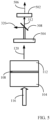
- FIG. 5 is an example of a microchip laser supporting fourth harmonic generation (FHG).
- the fourth harmonic generation is a process designed to produce UV-radiation for example at 266 nm or even shorter wavelengths.
- the fourth harmonic of Nd:YAG laser producing a laser beam with wavelength of 1064 nm would be a light beam with wavelength of 266 nm.
- Numeral 502 marks an FHG crystal and numeral 506 marks an output beam with wavelength of 266 nm.
- Such frequency conversation processes can offer a wide range of spectrum with sufficient energy for different spectroscopy application.
- this high energy microchip laser can provide higher energy/power at frequency converted wavelengths therefore significantly increase measurement precision by improving signal to noise ratio.
- the optical arrangement is very compact and simple.
- the disclosed high peak power microchip laser producing picosecond pulses could be used in many additional to spectroscopy fields. These include skin treatment, micromachining, efficient non-linear frequency conversation including harmonic generation (second harmonic, third harmonic, fourth harmonic, sum frequency generation, OPO, etc) and super continuum generation where the high peak power is required. Such frequency conversation processes can offer a wide range of spectrum with energy for spectroscopy application.
- the high energy short pulse microchip laser supports packaging of the microchip laser into a handpiece to perform meaningful aesthetic treatment and in particular fractional skin rejuvenation. It has been demonstrated clinically that for laser pulses of a few hundred picosecond with 4mJ per laser beam is sufficient enough to cause tissue or skin micro-injury through laser induced optical breakdown (LIOB) or melanin assistant optical breakdown. The subsequent collagen remodeling stimulated by such micro-injury will result in skin rejuvenation.
- LIOB laser induced optical breakdown
- the current microchip laser is capable to generate more than 40mJ 300ps laser pulses with wavelength of 1064nm.
- the output energy from the microchip laser can be split into for example, 10 micro-beams although other numbers of micro-beams are possible.
- Each micro-beam will have more than 4mJ which is sufficient for effective skin treatment.
- Each of the micro-beams could be focused by focusing optics to generate 10 micro-dots.
- Skin treatment usually requires irradiation of a two-dimensional skin area.
- Two dimensional micro-beam pattern for example, splitting the microchip laser beam into a one-dimensional array of micro-beams and manually sliding the one-dimensional array of micro-beams over the skin.
- Another approach is use of scanning system to scan the array of micro-beams in one or two direction/axes.
- Use of micro-beams or fractional beams with scanning mirrors or other scanning means supports fractional skin treatment.
- FIG. 6 is an example of a handpiece for fractional skin treatment.
- the exciting Alexandrite laser could be located in a cabinet and as disclosed in the US patent No. 9, 722,392 to the same assignee and inventor and incorporated herein in its entirety
- the Alexandrite pump laser beam schematically shown by arrow 606 could be conducted by a fiber optics connection to a seed microchip laser 610 located in handpiece body 604 configured to be applied to the skin.
- Handpiece body 604 could include a high energy seed microchip laser 610 identical to the described above microchip lasers and a unit of scanning mirrors 614 or a polygon spinner or other laser beam scanning means supporting laser beam 120 scanning in one or two directions or axes (X, Y). This would facilitate implementation of fractional skin treatment.
- the whole system of seed microchip laser 610 and scanning mirrors 614 could be small enough to be packed into handpiece 604.
- Such handpiece can generate picosecond laser allowing for fractional treatment for skin rejuvenation.
- Second or higher Harmonic Generator 304 could be located in handpiece body 604.
- Microchip laser 610 emits a beam with wavelength of 1064 nm.
- Second Harmonic Generator 304 could.be introduced into microchip laser beam path to generate an additional laser light wavelength.
- other wavelength frequency multiplying devices could be arranged on a turret and used when required.
- the caregiver or user could manually slide handpiece 604 with one-dimensional (1-D) beam splitter, for example, a holographic 1-D beamsplitter or scanner over the treated skin area forming a fractionated scanning system.
- one-dimensional (1-D) beam splitter for example, a holographic 1-D beamsplitter or scanner
- microchip seed laser 610 generates picosecond laser pulses forming a 1-D fractionated micro-dot 704 line.
- FIG. 7 is an example of a relatively sparse located fractionated micro-dot 704 in a 1-D line.
- Handpiece 604 movement speed 708 is higher than the same handpiece movement speed 808 ( FIG. 8 ). Accordingly, a denser 2-D pattern 812 of fractionated micro-dots 704 is generated.
- FIG. 9 a handpiece for fractional skin treatment is shown.
- Generation of a fractionated beam pattern is produced by a combination of a pair of galvanometer mirrors 904 and 908 that project or scan laser beam 120 onto a lens array 912.
- Lens array 912 splits laser beam 120 into a plurality of microbeams 916 which could also be fractionated microbeams.
- Mirror 920 could be used to separate additional wavelength generated by Second or higher Harmonic generator 304 could be located in harmonic generators.
- the coating of mirror 920 is formed accordingly to the desired wavelength separation.
- the unconverted infrared light 120 could be directed and absorbed in a laser light beam dump 924 while the harmonics could be delivered to the treated skin segment containing a combination of skin disorders.
- Laser light beam dump 924 could be designed to effectively dissipate the unconverted infrared energy without getting damaged or causing a rise in temperature of other handpiece 900 components. Passive and active cooling mechanisms can be used as need to remove heat from the laser light beam dump 924.
- Seed laser 610 energy could be 40mJ or more.
- the system is such designed that energy for each microbeam is up to 4mJ at 1064nm and 2mJ at 532nm.
- Such seed laser energy is high enough so that each laser beam from the seed laser can cover at least 9 lenslets to generate 9 micro-dots.
- Galvanometer mirror pair 904 and 908 scans the laser beam nine times to form a 2-D pattern and cover at least 81 lenslets. Assuming that microchip laser operates at a frequency of 20 Hz, each scan will take 0.45 second (9/20) or the treatment can be operated up to 2.2Hz.
- microchip laser and handpiece includes both combinations and subcombinations of various features described hereinabove as well as modifications and variations thereof which would occur to a person skilled in the art upon reading the foregoing description and which are not in the prior art.
- the present disclosure relates also to the following numbered items:
Landscapes
- Physics & Mathematics (AREA)
- Electromagnetism (AREA)
- Engineering & Computer Science (AREA)
- Optics & Photonics (AREA)
- Plasma & Fusion (AREA)
- Health & Medical Sciences (AREA)
- Life Sciences & Earth Sciences (AREA)
- Biomedical Technology (AREA)
- Chemical & Material Sciences (AREA)
- Crystallography & Structural Chemistry (AREA)
- General Health & Medical Sciences (AREA)
- Nuclear Medicine, Radiotherapy & Molecular Imaging (AREA)
- Animal Behavior & Ethology (AREA)
- Public Health (AREA)
- Veterinary Medicine (AREA)
- Radiology & Medical Imaging (AREA)
- Pathology (AREA)
- Surgery (AREA)
- Sustainable Development (AREA)
- Biophysics (AREA)
- Inorganic Chemistry (AREA)
- Otolaryngology (AREA)
- Heart & Thoracic Surgery (AREA)
- Molecular Biology (AREA)
- Medical Informatics (AREA)
- Ceramic Engineering (AREA)
- Lasers (AREA)
- General Physics & Mathematics (AREA)
- Laser Surgery Devices (AREA)
- Radiation-Therapy Devices (AREA)
Applications Claiming Priority (3)
| Application Number | Priority Date | Filing Date | Title |
|---|---|---|---|
| US16/015,249 US10622780B2 (en) | 2018-06-22 | 2018-06-22 | Handpiece with a microchip laser |
| PCT/US2019/037418 WO2019245937A1 (en) | 2018-06-22 | 2019-06-17 | Passively q-switched microchip laser with intra-cavity coating and hand piece with such a microchip laser |
| EP19734648.9A EP3811472A1 (de) | 2018-06-22 | 2019-06-17 | Passiv gütegeschalteter mikrochiplaser mit intrahohlraumbeschichtung und handstück mit einem solchen mikrochiplaser |
Related Parent Applications (1)
| Application Number | Title | Priority Date | Filing Date |
|---|---|---|---|
| EP19734648.9A Division EP3811472A1 (de) | 2018-06-22 | 2019-06-17 | Passiv gütegeschalteter mikrochiplaser mit intrahohlraumbeschichtung und handstück mit einem solchen mikrochiplaser |
Publications (2)
| Publication Number | Publication Date |
|---|---|
| EP4336678A2 true EP4336678A2 (de) | 2024-03-13 |
| EP4336678A3 EP4336678A3 (de) | 2024-06-05 |
Family
ID=67108227
Family Applications (3)
| Application Number | Title | Priority Date | Filing Date |
|---|---|---|---|
| EP24152441.2A Pending EP4336678A3 (de) | 2018-06-22 | 2019-06-17 | Handstück mit einem mikrochiplaser |
| EP19734648.9A Pending EP3811472A1 (de) | 2018-06-22 | 2019-06-17 | Passiv gütegeschalteter mikrochiplaser mit intrahohlraumbeschichtung und handstück mit einem solchen mikrochiplaser |
| EP24152452.9A Pending EP4340139A3 (de) | 2018-06-22 | 2019-06-17 | Lasersystem mit einem mikrochiplaser |
Family Applications After (2)
| Application Number | Title | Priority Date | Filing Date |
|---|---|---|---|
| EP19734648.9A Pending EP3811472A1 (de) | 2018-06-22 | 2019-06-17 | Passiv gütegeschalteter mikrochiplaser mit intrahohlraumbeschichtung und handstück mit einem solchen mikrochiplaser |
| EP24152452.9A Pending EP4340139A3 (de) | 2018-06-22 | 2019-06-17 | Lasersystem mit einem mikrochiplaser |
Country Status (7)
| Country | Link |
|---|---|
| US (2) | US10622780B2 (de) |
| EP (3) | EP4336678A3 (de) |
| JP (2) | JP2021530116A (de) |
| KR (1) | KR102773796B1 (de) |
| CN (1) | CN112425014B (de) |
| IL (3) | IL310191B2 (de) |
| WO (1) | WO2019245937A1 (de) |
Families Citing this family (11)
| Publication number | Priority date | Publication date | Assignee | Title |
|---|---|---|---|---|
| KR20170123862A (ko) * | 2016-04-29 | 2017-11-09 | 주식회사 루트로닉 | 레이저 빔 장치 및 이를 갖는 레이저 빔 핸드피스 |
| US10864380B1 (en) | 2020-02-29 | 2020-12-15 | Cutera, Inc. | Systems and methods for controlling therapeutic laser pulse duration |
| US11253720B2 (en) | 2020-02-29 | 2022-02-22 | Cutera, Inc. | Dermatological systems and methods with handpiece for coaxial pulse delivery and temperature sensing |
| CN111478166A (zh) * | 2020-04-21 | 2020-07-31 | 纬达星辰(深圳)科技有限公司 | 一种高能量皮秒级输出的固体脉冲激光器 |
| US11532919B2 (en) | 2020-05-27 | 2022-12-20 | Candela Corporation | Fractional handpiece with a passively Q-switched laser assembly |
| US12456848B2 (en) | 2020-05-27 | 2025-10-28 | Candela Corporation | Fractional handpiece with a passively Q-switched laser assembly |
| CN111769434A (zh) * | 2020-06-15 | 2020-10-13 | 北京工业大学 | 一种避免泵浦光漂白被动调q晶体的微片激光器 |
| JP2023175081A (ja) * | 2022-05-30 | 2023-12-12 | スパークリングフォトン株式会社 | 結晶型固体レーザー媒質複合体及びその製造方法 |
| CN116667122A (zh) * | 2023-07-31 | 2023-08-29 | 中国科学院长春光学精密机械与物理研究所 | 1.5μm波段芯片级半导体/固体垂直集成被动调Q激光器 |
| CN116683269A (zh) * | 2023-07-31 | 2023-09-01 | 中国科学院长春光学精密机械与物理研究所 | 1.06μm波段芯片级半导体/固体垂直集成被动调Q激光器 |
| KR102816452B1 (ko) * | 2024-08-21 | 2025-06-04 | 원텍 주식회사 | 고체 매질을 이용한 자외선 레이저 발생장치 |
Citations (1)
| Publication number | Priority date | Publication date | Assignee | Title |
|---|---|---|---|---|
| US9722392B2 (en) | 2013-11-28 | 2017-08-01 | Candela Corporation | Laser systems and related methods |
Family Cites Families (40)
| Publication number | Priority date | Publication date | Assignee | Title |
|---|---|---|---|---|
| FR2685135B1 (fr) * | 1991-12-16 | 1994-02-04 | Commissariat A Energie Atomique | Mini cavite laser pompee optiquement, son procede de fabrication et laser utilisant cette cavite. |
| US5394413A (en) * | 1994-02-08 | 1995-02-28 | Massachusetts Institute Of Technology | Passively Q-switched picosecond microlaser |
| US5847863A (en) * | 1996-04-25 | 1998-12-08 | Imra America, Inc. | Hybrid short-pulse amplifiers with phase-mismatch compensated pulse stretchers and compressors |
| FR2758915B1 (fr) * | 1997-01-30 | 1999-03-05 | Commissariat Energie Atomique | Microlaser solide declenche passivement par absorbant saturable et son procede de fabrication |
| US6219361B1 (en) * | 1999-06-21 | 2001-04-17 | Litton Systems, Inc. | Side pumped, Q-switched microlaser |
| US20030039274A1 (en) * | 2000-06-08 | 2003-02-27 | Joseph Neev | Method and apparatus for tissue treatment and modification |
| US6501772B1 (en) * | 2000-08-11 | 2002-12-31 | Litton Systems, Inc. | Microlaser assembly having a microresonator and aligned electro-optic components |
| JP2004121417A (ja) * | 2002-09-30 | 2004-04-22 | Nidek Co Ltd | レーザ治療装置 |
| EP1653876A1 (de) * | 2003-07-11 | 2006-05-10 | Reliant Technologies, Inc. | Verfahren und vorrichtung zur fraktionellen phototherapie von haut |
| US7814915B2 (en) * | 2006-03-03 | 2010-10-19 | Cutera, Inc. | Aesthetic treatment for wrinkle reduction and rejuvenation |
| KR100649890B1 (ko) * | 2006-03-27 | 2006-11-28 | 주식회사 루트로닉 | 접촉 센서를 이용한 레이저 빔 컨트롤 장치 및 컨트롤 방법 |
| KR100649889B1 (ko) * | 2006-03-27 | 2006-11-28 | 주식회사 루트로닉 | 미세 부분 박피를 위한 마이크로 레이저 빔의 조사 장치 및 조사 방법 |
| US20090227995A1 (en) * | 2006-09-29 | 2009-09-10 | Bhawalkar Jayant D | Precision Tube Assembly |
| ES2444141T3 (es) * | 2006-09-29 | 2014-02-24 | Candela Corporation | Un sistema de láser para tratamiento de la piel |
| US7649920B2 (en) * | 2007-04-03 | 2010-01-19 | Topcon Corporation | Q-switched microlaser apparatus and method for use |
| US8366703B2 (en) * | 2008-04-02 | 2013-02-05 | Cutera, Inc. | Fractional scanner for dermatological treatments |
| DE102008047640B4 (de) * | 2008-09-17 | 2012-10-25 | Anton Kasenbacher | Verwendung eines Laserbearbeitungsgeräts zur Ablation von Zahnmaterial |
| WO2010032235A1 (en) * | 2008-09-21 | 2010-03-25 | Syneron Medical Ltd. | A method and apparatus for personal skin treatment |
| JP5281922B2 (ja) * | 2009-02-25 | 2013-09-04 | 浜松ホトニクス株式会社 | パルスレーザ装置 |
| KR100960240B1 (ko) * | 2009-12-07 | 2010-06-03 | 주식회사 루트로닉 | 알렉산드라이트 레이저 펌프 챔버 |
| EP2577818B1 (de) * | 2010-05-28 | 2020-07-15 | Daniel Kopf | Ultrakurzpuls-mikrochiplaser, halbleiterlaser, lasersystem und pumpverfahren für dünne lasermedien |
| KR102005918B1 (ko) * | 2011-02-03 | 2019-07-31 | 트리아 뷰티, 인코포레이티드 | 방사선-계 피부치료 장치 |
| US20120283712A1 (en) * | 2011-02-03 | 2012-11-08 | TRIA Beauty | Devices and Methods for Radiation-Based Dermatological Treatments |
| IT1403871B1 (it) * | 2011-02-11 | 2013-11-08 | El En Spa | "dispositivo e metodo di trattamento laser della pelle" |
| US20130030506A1 (en) * | 2011-07-28 | 2013-01-31 | Conopco, Inc., D/B/A Unilever | Handholdable laser device featuring pulsing of a continuous wave laser |
| KR20130080598A (ko) * | 2012-01-05 | 2013-07-15 | 김도연 | 레이저를 이용한 골프용 경사 및 거리 측정기 |
| CA2861979C (en) * | 2012-01-23 | 2022-05-24 | Tomowave Laboratories, Inc. | Laser optoacoustic ultrasonic imaging system (louis) and methods of use |
| US9337609B2 (en) * | 2012-05-09 | 2016-05-10 | Mitsubishi Electric Corporation | Passively Q-switched element and passively Q-switched laser device |
| JP2014135421A (ja) * | 2013-01-11 | 2014-07-24 | Hamamatsu Photonics Kk | 固体レーザデバイス及びその製造方法 |
| KR101505083B1 (ko) * | 2013-04-11 | 2015-03-25 | 한국전기연구원 | 줄 레이저 빔이 조사되는 의료용 핸드피스 |
| AT515789B1 (de) * | 2014-07-07 | 2015-12-15 | Daniel Dr Kopf | Microchip-Laser |
| JP6456080B2 (ja) * | 2014-09-18 | 2019-01-23 | 株式会社トプコン | レーザ発振装置 |
| US20160143692A1 (en) * | 2014-11-22 | 2016-05-26 | Candela Corporation | Laser System For Skin Treatment |
| US9843157B2 (en) * | 2015-04-06 | 2017-12-12 | Voxtel, Inc. | Solid state laser system |
| CN205831906U (zh) * | 2015-09-30 | 2016-12-28 | 济南晶众光电科技有限公司 | 一种手持激光器 |
| JP2017220652A (ja) * | 2016-06-10 | 2017-12-14 | 大学共同利用機関法人自然科学研究機構 | レーザ装置とその製造方法 |
| WO2018108637A1 (en) * | 2016-12-12 | 2018-06-21 | Koninklijke Philips N.V. | Light based tissue treatment device |
| JP2018094155A (ja) * | 2016-12-14 | 2018-06-21 | 株式会社ユニタック | 皮膚レーザ治療器 |
| US9810775B1 (en) * | 2017-03-16 | 2017-11-07 | Luminar Technologies, Inc. | Q-switched laser for LIDAR system |
| US9810786B1 (en) * | 2017-03-16 | 2017-11-07 | Luminar Technologies, Inc. | Optical parametric oscillator for lidar system |
-
2018
- 2018-06-22 US US16/015,249 patent/US10622780B2/en active Active
-
2019
- 2019-06-17 EP EP24152441.2A patent/EP4336678A3/de active Pending
- 2019-06-17 CN CN201980047812.2A patent/CN112425014B/zh active Active
- 2019-06-17 IL IL310191A patent/IL310191B2/en unknown
- 2019-06-17 EP EP19734648.9A patent/EP3811472A1/de active Pending
- 2019-06-17 IL IL310192A patent/IL310192B2/en unknown
- 2019-06-17 EP EP24152452.9A patent/EP4340139A3/de active Pending
- 2019-06-17 IL IL279555A patent/IL279555B2/en unknown
- 2019-06-17 KR KR1020217000182A patent/KR102773796B1/ko active Active
- 2019-06-17 WO PCT/US2019/037418 patent/WO2019245937A1/en not_active Ceased
- 2019-06-17 JP JP2021520086A patent/JP2021530116A/ja active Pending
-
2020
- 2020-03-04 US US16/809,278 patent/US11271356B2/en active Active
-
2024
- 2024-03-06 JP JP2024034441A patent/JP2024063207A/ja active Pending
Patent Citations (1)
| Publication number | Priority date | Publication date | Assignee | Title |
|---|---|---|---|---|
| US9722392B2 (en) | 2013-11-28 | 2017-08-01 | Candela Corporation | Laser systems and related methods |
Non-Patent Citations (29)
| Title |
|---|
| A. AGNESI: "50-mJ macro-pulses at 1064 nm from a diode-pumped picosecond laser system", OPT. EXP., vol. 19, no. 21, 2011, pages 20316 |
| A. AGNESI: "Low-power 100-ps microchip laser amplified by a two-stage Nd:YVO4 amplifier module", APPL. PHYS. B, vol. 109, 2012, pages 659, XP035147640, DOI: 10.1007/s00340-012-5234-z |
| A. C. BUTLER: "Scaling Q-switched microchip lasers for shortest pulses", APPL. PHYS., vol. 109, 2012, pages 81, XP035134161, DOI: 10.1007/s00340-012-5223-2 |
| A. H. CURTIS: "Demonstration of a compact 100 Hz, 0.1 J diode-pumped picosecond laser", OPT. LETT., vol. 36, no. 11, 2011, pages 2164, XP001563396, DOI: 10.1364/OL.36.002164 |
| A. STEINMETZ: "Sub-5-ps, multimegawatt peak-power pulse from a fiber-amplified and optically compressed passively Q-switched microchip laser", OPT., vol. 37, no. 13, 2012, pages 2550, XP001576838, DOI: 10.1364/OL.37.002550 |
| A. STRATANL. RUSEN*R. DABUC. FENICC. BLANARU: "Picosecond laser system based on microchip oscillator", J. OPTO. ADV. MAT., vol. 10, no. 11, 2008, pages 3022 |
| C. WANG: "1.2 MW peak power, all-solid-state picosecond laser with a microchip laser seed and a high gain single-passing bounce geometry amplifier", OPTICS & LASER TECHNOLOGY, vol. 85, 2016, pages 14 |
| C.Y. CHO: "An energy adjustable linearly polarized passively Q-switched bulk laser with a wedged diffusion bonded Nd:YAG/Cr4+:YAG crystal", OPTICAL EXPRESS, vol. 23, no. 6, 2015, pages 8162 |
| E. TURKYILMAZ: "Simple ps microchip Nd:YV04 laser with 3.3-ps pulses at 0.2 to 1.4 MHz and single-stage amplification to the microjoule level", OPT. ENG., vol. 55, no. 6, 2016, pages 0661296 |
| G. SALAMU: "High Peak Power, Passively QSwitched, Composite, All Poly Crystalline Ceramics Nd:YAG/Cr4+:YAG Laser and Generation of 532 nm Green Light", SOLID STATE AND LIQUID LASERS, vol. 22, no. 1, 2012, pages 68 |
| H. HE: "Linearly polarized pumped passively Q-switched Nd:YVO4 microchip laser for Ince-Gaussian laser modes with controllable orientations", J. OPT., vol. 18, no. 12, 2016, pages 125202, XP020311229, DOI: 10.1088/2040-8978/18/12/125202 |
| J. DONG: "> 1 MW peak power, an efficient Yb:YAG/Cr4:YAG composite crystal passively Q-switched laser", LASER PHYSICS, vol. 24, 2014, pages 55801 |
| J. DONG: "A Cr4+:YAG passively Q-switched Nd:YVO4 microchip laser for controllable high-order Hermite-Gaussian modes", LASER PHYSICS, vol. 26, 2016, pages 095004 |
| J. NIKKINENVILLE-MARKUS KORPIJÄRVIIIRO LEINOANTTI HARKONENMIRCEA GUINA, FREQUENCY-DOUBLED PASSIVELY Q-SWITCHED MICROCHIP LASER PRODUCING 225 PS PULSES AT 671 NM, vol. 41, no. 22, 2016, pages 5385 |
| J. ZAYHOWSKI, Q-SWITCHED OPERATION OF MICROCHIP LASERS, vol. 16, no. 8, 1991, pages 575 |
| L. ZHENG: "MW peak power at 266 nm, low jitter kHz repetition rate from intense pumped microlaser", OPT. EXP., vol. 24, no. 25, 2016, pages 28748 |
| M. TSUNEKANE: "High Peak Power, Passively Q-switched Microlaser for Ignition of Engines", IEEE J. QUAN. ELEC., vol. 46, no. 2, 2010, pages 277, XP011288218, DOI: 10.1109/JQE.2009.2030967 |
| N. PAVEL: "Composite, all-ceramics, high-peak power Nd:YAG/Cr4+:YAG monolithic micro-laser with multiple-beam output for engine ignition", OPT. EXPRESS, vol. 19, no. 10, 2011, pages 9378 |
| O. SANDU: "High-peak power, passively Q-switched, composite, all-polycrystalline ceramic Nd:YAG/Cr4+ :YAG lasers", QUAN. ELEC., vol. 42, no. 3, 2012, pages 211 |
| P. LOIKO: "Sub-nanosecond Yb:KLu(W04)2 microchip laser", OPT. LETT., vol. 41, no. 11, 2016, pages 2620 |
| P. PEUSER: "Miniaturized, high-power diode-pumped, Q-switched Nd:YAG laser oscillator-amplifier", APPL. OPT., vol. 50, no. 4, 2011, pages 399, XP001560282, DOI: 10.1364/AO.50.000399 |
| Q. K. AIA: "Picosecond Nd:YLF FivePasses Laser Amplifier with 20 mJ Pulse Energy", SOLID STATE AND LIQUID LASERS, vol. 22, no. 7, 2012, pages 1169, XP035079828, DOI: 10.1134/S1054660X12070018 |
| R. BHANDARI: "> 6 MW peak power at 532 nm from passively Q-switched Nd:YAG/Cr4+:YAG microchip laser", OPT. EXP, vol. 19, no. 20, 2011, pages 19135 |
| R. BHANDARI: "> 6 MW peak power at 532 nm from passively Q-switched Nd:YAG/Cr4+:YAG microchip laser", OPTICAL EXPRESS, vol. 19, no. 20, 2011, pages 19135 |
| R. BHANDARI: "3 MW peak power at 266 nm using Nd:YAG/Cr4+:YAG microchip laser and fluxless-BBO", OPTICAL MATERIAL EXPRESS, vol. 2, no. 7, 2012, pages 907 |
| R. HARING: "Passively Q-switched microchip laser at 1.5 mm", J. OPT. SOC. AM. B., vol. 18, no. 12, 2001, pages 1805 |
| V. VITKIN: "Compact 0.7 mJ/11 ns eye-safe erbium laser", LASER PHYSICS, vol. 26, no. 12, 2016, pages 125801 |
| W. KONG: "Diode edge-pumped passively Q-switched microchip laser", OPT. ENG, vol. 54, no. 9, 2015, pages 090501, XP060072838, DOI: 10.1117/1.OE.54.9.090501 |
| X. GUO: "12 mJ Yb:YAG/Cr:YAG microchip laser", OPT. LETT., vol. 43, no. 3, 2018, pages 459 |
Also Published As
| Publication number | Publication date |
|---|---|
| EP4340139A3 (de) | 2024-06-05 |
| IL310191B1 (en) | 2024-04-01 |
| EP4340139A2 (de) | 2024-03-20 |
| JP2021530116A (ja) | 2021-11-04 |
| IL310192B2 (en) | 2024-08-01 |
| EP3811472A1 (de) | 2021-04-28 |
| US20200203913A1 (en) | 2020-06-25 |
| CN112425014A (zh) | 2021-02-26 |
| KR20210021345A (ko) | 2021-02-25 |
| US10622780B2 (en) | 2020-04-14 |
| JP2024063207A (ja) | 2024-05-10 |
| IL310192B1 (en) | 2024-04-01 |
| IL279555B2 (en) | 2025-04-01 |
| CN112425014B (zh) | 2024-07-02 |
| IL310192A (en) | 2024-03-01 |
| EP4336678A3 (de) | 2024-06-05 |
| WO2019245937A1 (en) | 2019-12-26 |
| IL310191A (en) | 2024-03-01 |
| IL279555A (en) | 2021-01-31 |
| KR102773796B1 (ko) | 2025-02-27 |
| IL279555B1 (en) | 2024-12-01 |
| US11271356B2 (en) | 2022-03-08 |
| US20190393668A1 (en) | 2019-12-26 |
| IL310191B2 (en) | 2024-08-01 |
Similar Documents
| Publication | Publication Date | Title |
|---|---|---|
| US11271356B2 (en) | Handpiece with a microchip laser | |
| EP4157126B1 (de) | Fraktioniertes handstück mit einer passiv gütegeschalteten laseranordnung | |
| JP3843374B2 (ja) | 受動的qスイッチピコ秒マイクロレーザー | |
| WO2002021643A2 (en) | MULTIWAVELENGTH lIGHT SOURCE USING AN OPTICAL PARAMETRIC OSCILLATOR | |
| Stolzenburg et al. | 700W intracavity-frequency doubled Yb: YAG thin-disk laser at 100 kHz repetition rate | |
| US12456848B2 (en) | Fractional handpiece with a passively Q-switched laser assembly | |
| US20240348002A1 (en) | Fractional handpiece with a passively q-switched laser assembly | |
| US20250387639A1 (en) | Fractional handpiece with a passively q-switched laser assembly with unstable cavity operation | |
| Spiekermann et al. | Ultraviolet single-frequency pulses with 485 mW average power | |
| Barnes et al. | Frequency-doubled 0.946-/spl mu/m Nd: YAG laser | |
| Shcheslavskiy et al. | Third-harmonic generation from Rayleigh particles: breaking all the rules | |
| Wintner | Ultrashort pulse solid-state lasers and modern applications | |
| Pinto et al. | Picosecond 2-um Tm: YAG laser | |
| Pasmanik | Shorter rods, shorter pulses |
Legal Events
| Date | Code | Title | Description |
|---|---|---|---|
| PUAI | Public reference made under article 153(3) epc to a published international application that has entered the european phase |
Free format text: ORIGINAL CODE: 0009012 |
|
| STAA | Information on the status of an ep patent application or granted ep patent |
Free format text: STATUS: THE APPLICATION HAS BEEN PUBLISHED |
|
| AC | Divisional application: reference to earlier application |
Ref document number: 3811472 Country of ref document: EP Kind code of ref document: P |
|
| AK | Designated contracting states |
Kind code of ref document: A2 Designated state(s): AL AT BE BG CH CY CZ DE DK EE ES FI FR GB GR HR HU IE IS IT LI LT LU LV MC MK MT NL NO PL PT RO RS SE SI SK SM TR |
|
| REG | Reference to a national code |
Ref country code: DE Ref legal event code: R079 Free format text: PREVIOUS MAIN CLASS: H01S0003000000 Ipc: H01S0003060000 |
|
| P01 | Opt-out of the competence of the unified patent court (upc) registered |
Effective date: 20240321 |
|
| PUAL | Search report despatched |
Free format text: ORIGINAL CODE: 0009013 |
|
| AK | Designated contracting states |
Kind code of ref document: A3 Designated state(s): AL AT BE BG CH CY CZ DE DK EE ES FI FR GB GR HR HU IE IS IT LI LT LU LV MC MK MT NL NO PL PT RO RS SE SI SK SM TR |
|
| RIC1 | Information provided on ipc code assigned before grant |
Ipc: A61N 5/067 20060101ALI20240427BHEP Ipc: A61N 5/06 20060101ALI20240427BHEP Ipc: A61B 18/20 20060101ALI20240427BHEP Ipc: H01S 3/00 20060101ALI20240427BHEP Ipc: H01S 3/113 20060101ALI20240427BHEP Ipc: H01S 3/094 20060101ALI20240427BHEP Ipc: H01S 3/06 20060101AFI20240427BHEP |
|
| STAA | Information on the status of an ep patent application or granted ep patent |
Free format text: STATUS: REQUEST FOR EXAMINATION WAS MADE |
|
| 17P | Request for examination filed |
Effective date: 20240917 |
|
| RBV | Designated contracting states (corrected) |
Designated state(s): AL AT BE BG CH CY CZ DE DK EE ES FI FR GB GR HR HU IE IS IT LI LT LU LV MC MK MT NL NO PL PT RO RS SE SI SK SM TR |
|
| RAP3 | Party data changed (applicant data changed or rights of an application transferred) |
Owner name: CANDELA CORPORATION |