EP4334133B1 - Verbessertes roll-to-roll-verarbeitungsverfahren - Google Patents
Verbessertes roll-to-roll-verarbeitungsverfahren Download PDFInfo
- Publication number
- EP4334133B1 EP4334133B1 EP22727355.4A EP22727355A EP4334133B1 EP 4334133 B1 EP4334133 B1 EP 4334133B1 EP 22727355 A EP22727355 A EP 22727355A EP 4334133 B1 EP4334133 B1 EP 4334133B1
- Authority
- EP
- European Patent Office
- Prior art keywords
- layer
- adhesive
- roll
- conductive elements
- carrier
- Prior art date
- Legal status (The legal status is an assumption and is not a legal conclusion. Google has not performed a legal analysis and makes no representation as to the accuracy of the status listed.)
- Active
Links
Images


Classifications
-
- H—ELECTRICITY
- H05—ELECTRIC TECHNIQUES NOT OTHERWISE PROVIDED FOR
- H05K—PRINTED CIRCUITS; CASINGS OR CONSTRUCTIONAL DETAILS OF ELECTRIC APPARATUS; MANUFACTURE OF ASSEMBLAGES OF ELECTRICAL COMPONENTS
- H05K3/00—Apparatus or processes for manufacturing printed circuits
- H05K3/02—Apparatus or processes for manufacturing printed circuits in which the conductive material is applied to the surface of the insulating support and is thereafter removed from such areas of the surface which are not intended for current conducting or shielding
- H05K3/04—Apparatus or processes for manufacturing printed circuits in which the conductive material is applied to the surface of the insulating support and is thereafter removed from such areas of the surface which are not intended for current conducting or shielding the conductive material being removed mechanically, e.g. by punching
- H05K3/043—Apparatus or processes for manufacturing printed circuits in which the conductive material is applied to the surface of the insulating support and is thereafter removed from such areas of the surface which are not intended for current conducting or shielding the conductive material being removed mechanically, e.g. by punching by using a moving tool for milling or cutting the conductive material
-
- B—PERFORMING OPERATIONS; TRANSPORTING
- B32—LAYERED PRODUCTS
- B32B—LAYERED PRODUCTS, i.e. PRODUCTS BUILT-UP OF STRATA OF FLAT OR NON-FLAT, e.g. CELLULAR OR HONEYCOMB, FORM
- B32B37/00—Methods or apparatus for laminating, e.g. by curing or by ultrasonic bonding
- B32B37/12—Methods or apparatus for laminating, e.g. by curing or by ultrasonic bonding characterised by using adhesives
- B32B37/1284—Application of adhesive
-
- B—PERFORMING OPERATIONS; TRANSPORTING
- B32—LAYERED PRODUCTS
- B32B—LAYERED PRODUCTS, i.e. PRODUCTS BUILT-UP OF STRATA OF FLAT OR NON-FLAT, e.g. CELLULAR OR HONEYCOMB, FORM
- B32B37/00—Methods or apparatus for laminating, e.g. by curing or by ultrasonic bonding
- B32B37/14—Methods or apparatus for laminating, e.g. by curing or by ultrasonic bonding characterised by the properties of the layers
- B32B37/16—Methods or apparatus for laminating, e.g. by curing or by ultrasonic bonding characterised by the properties of the layers with all layers existing as coherent layers before laminating
- B32B37/20—Methods or apparatus for laminating, e.g. by curing or by ultrasonic bonding characterised by the properties of the layers with all layers existing as coherent layers before laminating involving the assembly of continuous webs only
-
- B—PERFORMING OPERATIONS; TRANSPORTING
- B32—LAYERED PRODUCTS
- B32B—LAYERED PRODUCTS, i.e. PRODUCTS BUILT-UP OF STRATA OF FLAT OR NON-FLAT, e.g. CELLULAR OR HONEYCOMB, FORM
- B32B38/00—Ancillary operations in connection with laminating processes
- B32B38/0004—Cutting, tearing or severing, e.g. bursting; Cutter details
-
- B—PERFORMING OPERATIONS; TRANSPORTING
- B32—LAYERED PRODUCTS
- B32B—LAYERED PRODUCTS, i.e. PRODUCTS BUILT-UP OF STRATA OF FLAT OR NON-FLAT, e.g. CELLULAR OR HONEYCOMB, FORM
- B32B38/00—Ancillary operations in connection with laminating processes
- B32B38/10—Removing layers, or parts of layers, mechanically or chemically
- B32B38/105—Removing layers, or parts of layers, mechanically or chemically on edges
-
- B—PERFORMING OPERATIONS; TRANSPORTING
- B32—LAYERED PRODUCTS
- B32B—LAYERED PRODUCTS, i.e. PRODUCTS BUILT-UP OF STRATA OF FLAT OR NON-FLAT, e.g. CELLULAR OR HONEYCOMB, FORM
- B32B43/00—Operations specially adapted for layered products and not otherwise provided for, e.g. repairing; Apparatus therefor
- B32B43/003—Cutting
-
- H—ELECTRICITY
- H05—ELECTRIC TECHNIQUES NOT OTHERWISE PROVIDED FOR
- H05K—PRINTED CIRCUITS; CASINGS OR CONSTRUCTIONAL DETAILS OF ELECTRIC APPARATUS; MANUFACTURE OF ASSEMBLAGES OF ELECTRICAL COMPONENTS
- H05K1/00—Printed circuits
- H05K1/02—Details
- H05K1/03—Use of materials for the substrate
- H05K1/0313—Organic insulating material
-
- H—ELECTRICITY
- H05—ELECTRIC TECHNIQUES NOT OTHERWISE PROVIDED FOR
- H05K—PRINTED CIRCUITS; CASINGS OR CONSTRUCTIONAL DETAILS OF ELECTRIC APPARATUS; MANUFACTURE OF ASSEMBLAGES OF ELECTRICAL COMPONENTS
- H05K3/00—Apparatus or processes for manufacturing printed circuits
- H05K3/02—Apparatus or processes for manufacturing printed circuits in which the conductive material is applied to the surface of the insulating support and is thereafter removed from such areas of the surface which are not intended for current conducting or shielding
- H05K3/027—Apparatus or processes for manufacturing printed circuits in which the conductive material is applied to the surface of the insulating support and is thereafter removed from such areas of the surface which are not intended for current conducting or shielding the conductive material being removed by irradiation, e.g. by photons, alpha or beta particles
-
- H—ELECTRICITY
- H05—ELECTRIC TECHNIQUES NOT OTHERWISE PROVIDED FOR
- H05K—PRINTED CIRCUITS; CASINGS OR CONSTRUCTIONAL DETAILS OF ELECTRIC APPARATUS; MANUFACTURE OF ASSEMBLAGES OF ELECTRICAL COMPONENTS
- H05K3/00—Apparatus or processes for manufacturing printed circuits
- H05K3/02—Apparatus or processes for manufacturing printed circuits in which the conductive material is applied to the surface of the insulating support and is thereafter removed from such areas of the surface which are not intended for current conducting or shielding
- H05K3/04—Apparatus or processes for manufacturing printed circuits in which the conductive material is applied to the surface of the insulating support and is thereafter removed from such areas of the surface which are not intended for current conducting or shielding the conductive material being removed mechanically, e.g. by punching
- H05K3/046—Apparatus or processes for manufacturing printed circuits in which the conductive material is applied to the surface of the insulating support and is thereafter removed from such areas of the surface which are not intended for current conducting or shielding the conductive material being removed mechanically, e.g. by punching by selective transfer or selective detachment of a conductive layer
- H05K3/048—Apparatus or processes for manufacturing printed circuits in which the conductive material is applied to the surface of the insulating support and is thereafter removed from such areas of the surface which are not intended for current conducting or shielding the conductive material being removed mechanically, e.g. by punching by selective transfer or selective detachment of a conductive layer using a lift-off resist pattern or a release layer pattern
-
- H—ELECTRICITY
- H10—SEMICONDUCTOR DEVICES; ELECTRIC SOLID-STATE DEVICES NOT OTHERWISE PROVIDED FOR
- H10D—INORGANIC ELECTRIC SEMICONDUCTOR DEVICES
- H10D84/00—Integrated devices formed in or on semiconductor substrates that comprise only semiconducting layers, e.g. on Si wafers or on GaAs-on-Si wafers
- H10D84/01—Manufacture or treatment
-
- H10P14/40—
-
- B—PERFORMING OPERATIONS; TRANSPORTING
- B32—LAYERED PRODUCTS
- B32B—LAYERED PRODUCTS, i.e. PRODUCTS BUILT-UP OF STRATA OF FLAT OR NON-FLAT, e.g. CELLULAR OR HONEYCOMB, FORM
- B32B2307/00—Properties of the layers or laminate
- B32B2307/20—Properties of the layers or laminate having particular electrical or magnetic properties, e.g. piezoelectric
- B32B2307/202—Conductive
-
- B—PERFORMING OPERATIONS; TRANSPORTING
- B32—LAYERED PRODUCTS
- B32B—LAYERED PRODUCTS, i.e. PRODUCTS BUILT-UP OF STRATA OF FLAT OR NON-FLAT, e.g. CELLULAR OR HONEYCOMB, FORM
- B32B37/00—Methods or apparatus for laminating, e.g. by curing or by ultrasonic bonding
- B32B37/02—Methods or apparatus for laminating, e.g. by curing or by ultrasonic bonding characterised by a sequence of laminating steps, e.g. by adding new layers at consecutive laminating stations
-
- B—PERFORMING OPERATIONS; TRANSPORTING
- B32—LAYERED PRODUCTS
- B32B—LAYERED PRODUCTS, i.e. PRODUCTS BUILT-UP OF STRATA OF FLAT OR NON-FLAT, e.g. CELLULAR OR HONEYCOMB, FORM
- B32B38/00—Ancillary operations in connection with laminating processes
- B32B38/10—Removing layers, or parts of layers, mechanically or chemically
-
- H—ELECTRICITY
- H05—ELECTRIC TECHNIQUES NOT OTHERWISE PROVIDED FOR
- H05K—PRINTED CIRCUITS; CASINGS OR CONSTRUCTIONAL DETAILS OF ELECTRIC APPARATUS; MANUFACTURE OF ASSEMBLAGES OF ELECTRICAL COMPONENTS
- H05K1/00—Printed circuits
- H05K1/02—Details
- H05K1/03—Use of materials for the substrate
- H05K1/0393—Flexible materials
-
- H—ELECTRICITY
- H05—ELECTRIC TECHNIQUES NOT OTHERWISE PROVIDED FOR
- H05K—PRINTED CIRCUITS; CASINGS OR CONSTRUCTIONAL DETAILS OF ELECTRIC APPARATUS; MANUFACTURE OF ASSEMBLAGES OF ELECTRICAL COMPONENTS
- H05K2203/00—Indexing scheme relating to apparatus or processes for manufacturing printed circuits covered by H05K3/00
- H05K2203/15—Position of the PCB during processing
- H05K2203/1545—Continuous processing, i.e. involving rolls moving a band-like or solid carrier along a continuous production path
Definitions
- This invention relates to roll-to-roll processing methods, and particularly to a roll-to-roll processing method for providing a conductive element on a receiving carrier web.
- the receiving carrier needs to be elastic and/or stretchable so that it can be, for example, comfortably worn.
- the receiving carrier needs to have a web-like form so that it can be roll-to-roll processed but is also elastically deformable so that it appropriately follows contours and deformations of a curved surface on which it is to be subsequently fixed.
- additional reinforcing and/or carrier layers between the conductive element and the receiving carrier are simply not acceptable. For example, when a patterned element formed of a layer of conductive metal and a layer of reinforcing paper material is placed on a fabric, the fabric no longer bends in a way it should in order to be comfortably worn.
- Deformability of the receiving carrier is not the only characteristic that is compromised by an intermediate layer under the conductive element.
- thickness or coverage of the element placed on the receiving carrier is of importance and use of additional reinforcing sheets to transfer the conductive element on such receiving carrier web is problematic or even impossible. This is the case with, for example, functional conductive elements laminated on or between layers of kraft paper.
- the conductive element introduced into the laminate needs to be as thin as possible to avoid adverse effect to the appearance and functionality of the laminate.
- US 2014/0338739 A1 discloses a roll-to-roll processing method for manufacturing an integrated back-sheet for a back contact photovoltaic module with a metal foil circuit adhered to a polymer substrate.
- An object of the present disclosure is to provide a solution that solves or at least alleviates the above challenges in providing conductive elements on many types of carrier webs.
- the disclosed embodiments are based on the idea of operating systematically with two different types of adhesives in selected stages of the roll-to-roll processing.
- An advantage of the proposed solutions is that a very thin element of conductive material can be accurately and reliably transferred to adhesively attach on a carrier surface.
- Roll-to-roll processing is a fabrication method used for manufacturing products.
- a web of materials can be continuously fed from one reel onto another and at the same time materials can added to the progressing web or removed from it to produce a desired product.
- FIG. 1 illustrates stages of an example of a roll-to-roll processing method applying the claimed invention. It is to be noted that the drawings included in this specification are schematic figures, which show only structural elements that are necessary to explain the non-restrictive examples of the claimed method. It is clear that implementations of the roll-to-roll processing method may include several additional stages and conventional parts that are well known to a person skilled in the art and will thus not be discussed in detail herein.
- the roll-to-roll processing method disclosed in this text includes patterning boundaries of one or more conductive elements into a layered web that includes a conducting layer and a first substrate layer bound to each other with a first adhesive. Boundaries of one or more conductive elements are patterned so that said patterning includes cutting the boundaries through the conducting layer but not through the first substrate layer. Parts of the conducting layer outside the boundaries of the one or more conductive elements are removed from the first substrate layer and top surfaces of the one or more conductive elements to a second substrate layer with a second adhesive. In the end, a resulting layered web that includes at least the second substrate and the conductive elements is rolled on a reel.
- the first substrate layer is a sacrificial substrate layer and the first adhesive is a releasably binding adhesive.
- the second substrate is a first carrier layer and the second adhesive is a carrier binding adhesive.
- the term layer refers in this text to an elongate web of material that can be rolled around a reel for a roll-to-roll process.
- a conducting layer refers here to an elastic elongate sheet with a tensile strength that enables it to be roll-to-roll processed as a continuous web but is thin and thus flexible enough to not have substantial effect on mechanical properties of an underlying surface when attached to it.
- the conducting layer may be made of a material (e.g. metal) that provides both the required conductivity and the required tensile strength, but for the required conductivity, the conducting layer typically includes a very thin layer of conductive material on a thin polymer web.
- the conductive material may be metal or some metal composition including conductive metals.
- conductive metals include aluminum, copper, silver, platinum, palladium, zinc, nickel, gold, chromium, iron, molybdenum and equals and their alloys.
- the polymer web may include plastics based on polymers, their copolymers and mixtures, for example, poly(ethylene terphtalate), poly(naphtalene), poly(methyl methacrylate), poly(imide), poly(ethylene), cyclo-olephinic polymers and -co-polymers, thermoplastic urethane, poly(carbonate), poly(propylene), poly(vinyl chloride), poly(tetra fluoro ethane) and similar, silicones, or the like.
- the thickness of the layer of conductive material is of the order of 0.5 to 50 micrometers and the thickness of the polymer film is of the order of 10 to 250 micrometers.
- the layer of conductive material is of the order of 10 to 30 micrometers and the thickness of the polymer film is of the order of 10 to 125 micrometers. In some other layer structures, the layer of conductive material is of the order of 10 to 20 micrometers and the thickness of the polymer film is of the order of 20 to 50 micrometers.
- Very successful applications have been made with, for example, a conducting layer that contains a 12 micrometer layer of aluminum on a 36 micrometer layer of polyethylene terephthalate (PET), but the manufacturing process described herein enables application of even thinner conducting layers. With thicknesses in this range, the polymer film provides at least 90 % of the tensile strength of the conducting layer.
- this type of polymer film can be provided with a thickness that provides a necessary tensile strength for transferring the conducting layer laminate as such from reel to reel and also to appropriately endure the force required to release the adhesion of the releasably binding adhesive. Even so, the conducting layer is still thin and flexible enough to not notably compromise web-like mechanical properties, like flexibility, of the receiving carrier when finally fixed on it. It has been detected that to be durable enough for efficient processing, paper materials need to be so thick that their existence on a flexible receiving carrier significantly stiffens the web-like form, and thus makes the resulting receiving carrier unsuitable for purposes where elastic conformity is required. Furthermore, use of reinforcing sheet of paper tends to be problematic for applications, where added thickness by the conductive element needs to be minimized.
- the sacrificial substrate layer refers here to a reinforcing layer on which the conducting layer remains releasably bonded through patterning and material releasing stages that will be described in detail later in this text.
- the sacrificial substrate layer is the reinforcing element that provides more than 60% of the tensile strength of the layered web and is therefore considerably (at least two times) thicker than the conducting layer.
- sacrificial substrate layer examples include plastics based on polymers, their copolymers and mixtures, for example, poly(ethylene terphtalate), poly(naphtalene), poly(methyl methacrylate), poly(imide), poly(ethylene), cyclo-olephinic polymers and o-polymers, thermoplastic urethane, poly(carbonate), poly(propylene), poly(vinyl chloride), poly(tetra fluoro ethane) and similar, silicones, or the like.
- Very successful implementations have already been made with, for example, a sacrificial substrate layer of 0.08 millimeter polyester film.
- the sacrificial substrate layer may also include some other reinforcing material, like a paper sheet that is covered with a thin layer of plastic materials, like the ones listed above.
- the sacrificial substrate layer and the conducting layer are laminated into a temporary composite structure by gluing their surfaces to each other with a releasably binding adhesive.
- Releasably binding adhesive in this context refers to any adhesive that binds the sacrificial substrate layer and the conducting layer to each other so that they remain fastened while boundaries of a conductive element are pattered into the conducting layer, but so that the adhesion of the releasably binding adhesive can be released by pulling the surfaces of the sacrificial substrate layer and the conducting layer away from each other with a force that does not break either of the layers.
- releasably binding adhesives examples include silicones, acrylates, epoxides, urethanes, or poly(vinyls) that can be deposited on the sacrificial substrate layer by lamination, spraying, coating, printing or as a hotmelt glue.
- the conducting layer 100 is rolled out of one reel 102 and the sacrificial substrate layer 104 is rolled out of another reel 106 and the layers are pressed on each other with nip rolls 108.
- the layers 100, 104 can be laminated to each other in beforehand, and fed to the roll-to-roll process in a readily laminated form.
- the sacrificial substrate layer 104 is covered by a layer of the releasably binding adhesive.
- the roll-to-roll process is shown to include a spray station 110 in which the releasably binding adhesive is spread on the sacrificial substrate layer after it is rolled out the reel 106.
- the mechanism for providing the releasably binding adhesive is not relevant, as such.
- Examples of other applicable deposition methods include flexography, gravure, wire printing, off-set printing, screen printing, slot-die and reverse-gravure, among others.
- the sacrificial substrate layer may even be provided as readily covered with releasably binding adhesive and a protective sheet that is reeled off before the sacrificial substrate layer is fed into the process.
- the essential aspect is that the releasably binding adhesive is provided between a surface of the conducting layer 100 and a surface of the sacrificial substrate layer 104 so that when the surfaces are put into contact, the releasable adhesion activates or can be activated to releasably bind the surfaces to each other.
- the releasably binding adhesive can alternatively be deposited on a surface of the conducting layer.
- Activation of the releasably binding adhesive refers here to any function that completes the binding effect of the releasably binding adhesive. Examples of applicable activation methods to bond an adhesive with the adherent include, for example, application of pressure, enabling contact, cooling, heating, radiation, to mention some.
- the layer of conductive material provides the surface of the conducting layer that is put against the surface of the sacrificial substrate layer.
- the polymer film becomes then positioned to the side in which the patterning cuts through the conducting layer. This provides a protecting effect that ensures that the resulting pattern, which is cut from the layer of conductive materials, is more accurately in the designed form.
- Figure 1 illustrates the patterning stage with a cutting tool 112.
- a cutting tool that patterns a layered web by means of force typically includes a die that shears the layered web to a predefined depth.
- the patterning is configured to cut the boundaries of conductive elements through the conducting layer but not through the sacrificial substrate layer.
- This kind of cutting method is known in the field as kiss-cutting.
- the die of a kiss-cutting tool may be, for example, a rotary flexible die or a solid die.
- alternative kiss-cutting mechanisms may be applied within the scope.
- a beam of a high-power laser can be directed on the layered web for the purpose of laser-cutting through the conducting layer but not through the sacrificial substrate layer.
- FIG 1 provides a simplified illustration of a cutting tool 112, an example of which is discussed in more detail with Figure 2.
- Figure 2 shows an exploded view to layers of the roll-to-roll processed web and exemplary parts of the cutting tool.
- the cutting tool may include a cutting reel 200 and an anvil reel 202.
- the cutting reel 200 includes at least one cutting die, typically a matrix of dies that extend to a defined distance from the cutting reel 200. During operation, the cutting reel is rotated and pressed against the anvil reel 202.
- a depth dimensioning mechanism that controls the distance between the rotating wheel 200 and the anvil reel 202, and thus adjusts the cutting depth at a predefined level.
- a simple example of a depth dimensioning mechanism is a set of height-adjustable rigid sleeves that run in the edge of the anvil reel and during operation stop the cutting reel into abutment with their adjusted height.
- the boundaries of the conductive elements form a continuous pattern so that after the patterning stage, the conductive elements are separated from the conducting layer as single elements and the parts of the conducting layer outside these boundaries form a continuous recessed web 114.
- the recessed web 114 can be removed from the roll-to-roll processed web by releasing it from the sacrificial substrate layer and rolling it on a release reel 116 that is offset from the direction of progress of the roll-to-roll processed web.
- the parts of the conducting layer, which form the recessed web become thus pulled away from the sacrificial substrate layer with a force that exceeds adhesion of the releasably binding adhesive. This is enabled by the tensile strength of the conducting layer, in this example, the tensile strength of the polymer film, and the appropriately weak adhesion of the releasably binding adhesive.
- the adhesion needs to be strong enough to support the very thin conducting layer during the cutting operation so that accuracy of the boundaries of the resulting pattern is adequate.
- the releasably binding adhesive needs to be weak enough to enable release of the recessed web 114.
- the roll-to-roll processed web After removal of the recessed web, the roll-to-roll processed web includes the sacrificial substrate layer and conductive elements attached on it with the releasably binding adhesive.
- bottom surfaces of the conductive elements are bound to the sacrificial substrate layer with the releasably binding adhesive, and top surfaces of the conductive elements are exposed. These top surfaces can then be bound to a first carrier layer, which is now a receiving carrier, with a carrier binding adhesive.
- the example of Figure 1 shows an exemplary embodiment wherein a film of the carrier binding adhesive is formed first on the first carrier layer 122. This is illustrated by showing a spray station 118 in which the releasably binding adhesive is spread on the first carrier layer after it is rolled out the reel 120.
- the mechanism for providing the carrier binding adhesive is not relevant, as such.
- the essential aspect is that the carrier binding adhesive is provided between a surface of the first carrier layer 122 and top surfaces of the conductive elements so that when these surfaces are put into contact, the more permanent carrier binding adhesive can be activated to bind the surfaces to each other.
- the other essential aspect is that the two adhesives are selected or otherwise arranged so that adhesion between the conductive elements and the first carrier layer by the carrier binding adhesive is stronger than adhesion between the conductive elements and the sacrificial substrate layer by the releasably binding adhesive.
- the first carrier layer 122 preferably includes a web of fibres on which at least one conductive element is to be attached.
- the web of fibres may be a woven web formed of a network of interlocked fibres or a non-woven web formed of fibres bonded together by chemical, mechanical, heat or solvent treatment.
- Said fibres can include natural or synthetic, for example, animal based fibres (e.g. hair, fur, skin, silk, etc.), plant-based fibres (e.g. pulpwood trees, cotton, straw, bamboo, etc.), mineral based fibres (e.g., basalt, glass, metal) or synthetic fibres (e.g. polyester, aramid, acrylic, nylon, carbon, etc.).
- carrier binding adhesive refers in this context to any adhesive that does not harden in use and forms a strong adhesion between the first carrier layer 122 and the top surfaces of the conductive elements. Essentially, the adhesion by the carrier binding adhesive is stronger than the adhesion between the bottom surfaces of the conductive elements and the sacrificial substrate layer 104 formed with the releasably binding adhesive.
- the carrier binding adhesives include silicones, acrylates, epoxides, urethanes, poly(vinyls), to mention some.
- adhesion of the carrier binding adhesive can be activated so that the conductive elements become firmly bonded to the surface of the first carrier layer 122.
- the sacrificial substrate layer can be removed from the one or more conductive elements. Due to the higher adhesive bond between the first carrier layer 122 and the top surfaces of the conductive elements than between the bottom surfaces of the conductive elements and the sacrificial substrate layer 104, this can be implemented simply by pulling the sacrificial substrate layer 104 away from the one or more conductive elements with a reel 124 that is offset from the direction of the roll-to-roll processed web. This creates a force that exceeds adhesion of the releasably binding adhesive but not the adhesion of the carrier binding adhesive. The stronger adhesion of the carrier binding adhesive keeps the conductive elements secured on the first carrier layer 122 while the releasably binding adhesive lets the sacrificial substrate layer to be released from the bottom surfaces of the conductive elements.
- the roll-to-roll processed web includes only the conductive elements easily transferred and now firmly bound on the first carrier layer 122 without intermediate stiffening sheets, like reinforcing paper layers, that would adversely affect the elastic properties or structural integrity of the first carrier layer or increase the thickness of the resulting laminate.
- the resulting combination could already be used as a product that contains a receiving carrier and one or more conductive elements.
- Figure 1 illustrates further optional stages that can be used to provide a laminate wherein the conductive element is fixed between two carrier layers, still without intermediate stiffening and height increasing elements.
- the roll-to-roll process can include a further stage wherein the bottom surfaces of the one or more conductive elements are bound to a third substrate layer with a third adhesive.
- the bottom surfaces of the one or more conductive elements are surfaces of the conducting layer exposed by removing the first substrate layer from them.
- said third substrate layer is a second carrier layer 126 and the third adhesive is the carrier binding adhesive.
- the second carrier layer can be rolled off a reel 128 and a layer of the carrier binding adhesive be applied on a surface of the second carrier layer. This is illustrated by showing a spray station 130 in which the releasably binding adhesive is spread on the second carrier layer after it is rolled out the reel 128.
- the mechanism for providing the carrier binding adhesive is not relevant, as such.
- Alternative deposition methods include flexograph-, gravure-, offset or screen printing, slot-die or reverse gravure coating, for example.
- the essential aspect is that the carrier binding adhesive is provided between a surface of the second carrier layer 128 and bottom surfaces of the conductive elements so that when these surfaces are put into contact between reels 134, the carrier binding adhesive can be activated to bind the surfaces to each other.
- the resulting laminate can then be rolled as a final dual-laminate product on a transfer reel 136.
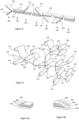
- Figure 3 illustrates an embodiment showing an alternative way to bind the top surfaces of the one or more conductive elements to a first carrier layer with a carrier binding adhesive.
- Elements and stages that were shown and explained in Figure 1 are denoted in Figure 3 with same reference numbers and are not described with this drawing again, further details on these elements can be referred from the description of Figure 1 .
- a layer of the carrier binding adhesive is formed on the layered web before the patterning stage.
- the top surfaces of the one or more conductive elements are bound to the first carrier layer by activating adhesion of the carrier binding adhesive after the patterning stage where boundaries of the conductive elements are patterned into the layered web but before the removing stage where the parts of the conducting layer outside the boundaries of the one or more conductive elements are removed from the sacrificial substrate layer.
- PSA pressure sensitive adhesive
- PSA adhesives include acrylic and silicone based PSA tapes.
- Many of the PSA products can be roll-to-roll processed, and they are also well applicable in die-cutting and kiss-cutting processes because they typically appear in solid but elastic form that is easy to cut and does not spatter or stick on the cutting tools.
- acrylic-based PSA products are of the type that provides an appropriate adhesive strength for the purpose. In practise this means that the adhesion by acrylic-based PSA is so much stronger than the adhesive strength of the releasably binding adhesive that it keeps the conductive elements fixed to the first carrier layer even when the sacrificial substrate layer is released by pulling it away from them.
- a PSA tape needs to be covered with a release liner, like a silicone covered polymer film.
- Figure 3 shows an implementation where the roll-to-roll process disclosed in Figure 1 includes a further PSA reel 140 from which a PSA tape 142, which includes a layer of PSA material covered with a release liner is rolled on the layered sheet that rolls out of the nip rolls 108.
- the PSA tape is oriented so that the layer of PSA material gets into contact with the conducting layer conductor layer of the layered web and the release liner is on the top.
- the layered web and the PSA tape are pressed together with nip rolls 144, which activates the PSA material, and forms the strong adhesion to the conducting layer in layered web.
- the release liner can then be removed as a continuous sheet with a reel 146, as shown in Figure 3 .
- the PSA material now forms the carrier binding adhesive, covers the conducting layer, and becomes patterned with it in the cutting tool 112. Parts of the PSA material layer become also removed from the process with the removable parts of the conducting layer when the recessed web is released from the sacrificial substrate layer by means of the reel 116.
- the roll-to-roll processed web includes the sacrificial substrate layer and the conductive elements. Bottom surfaces of the conductive elements are bound to the sacrificial substrate layer with the releasably binding adhesive, and top surfaces of the conductive elements are covered with a layer of PSA material.
- the roll-to-roll processed web is now put into contact with the first carrier layer 122 rolling out of reel 120 and pressed on it with nip rolls 148, the top surfaces of the conductive elements become strongly fixed to the first carrier layer 122, and the sacrificial substrate layer 104 can be pulled off by rolling it onto the reel 124, as described in Figure 1 .
- the adhesion by the releasably binding adhesive is so much weaker than the adhesion by the PSA material of the carrier binding adhesive that the conductive elements remain fixed to the first carrier layer while the sacrificial substrate layer 104 is released from the roll-to-roll processed web.
- the process may optionally include a further pair of nip rolls 134 to finalise the desired lamination and the final product that includes the flexible web of the first carrier sheet with flexible conductive elements without stiffening and/or height increasing reinforcing layers can then be rolled onto a transfer reel 136.
- FIG. 4 illustrates in simplified form stages of the roll-to-roll process described in detail with Figure 1 . Further details for the terms and elements discussed herein may be referred from the description of Figure 1 .
- the layered web is formed by binding the conducting layer 402 and the sacrificial substrate layer 404 to each other with the releasably binding adhesive.
- Stage 410 illustrates the patterning stage wherein a cutting tool 412 patterns boundaries of the conductive elements into the layered web 414 by cutting though the conducting layer but not through the sacrificial substrate layer.
- Stage 420 illustrates removal of the recessed web 422, formed of the parts of the conducting layer outside the boundaries of the one or more conductive elements from the sacrificial substrate layer.
- Stage 430 illustrates binding the exposed top surfaces 432 of the conductive elements to the first carrier layer 434, which is covered with the carrier binding adhesive.
- Stage 440 illustrates removal of the sacrificial substrate layer 442 from the one or more conductive elements while the top surfaces of the one or more conductive elements are already bound to the first carrier layer 444.
- Stage 450 illustrates the optional function to create a dual-sided laminate by binding the exposed bottom surfaces 452 of the conductive elements to the second carrier layer 454, which is covered with the carrier binding adhesive.
- Stage 460 illustrates rolling of the resulting dual-layer product that includes one or more flexible conductive elements laminated inside two flexible fibrous webs.
- Figure 5 illustrates an embodiment showing a further alternative way to bind the top surfaces of the one or more conductive elements to a first carrier layer with a carrier binding adhesive so that roll-to-roll processable PSA material can be used as a carrier binding adhesive in both adhesive layers of a dual-laminate product.
- a layer of the carrier binding adhesive is a PSA tape that it is rolled from a reel onto the conductive elements after the patterning stage.
- the top surfaces of the one or more conductive elements are bound to the first carrier layer before the removing stage where the parts of the conducting layer outside the boundaries of the one or more conductive elements are removed from the sacrificial substrate layer.
- Figure 5 shows an implementation where the roll-to-roll process disclosed in Figures 1 and 3 includes a further PSA reel 160 from which a PSA tape 162, which includes a layer of PSA material covered with a release liner is rolled on the first carrier layer 122 rolling out of reel 120.
- the first carrier layer 122 and the PSA tape are pressed together with nip rolls 164, which activates the PSA material, and forms the strong adhesion to the first carrier layer 122.
- the release liner can then be removed as a continuous sheet with a reel 166, as shown in Figure 5 .
- the PSA material layer now forms the carrier binding adhesive, and is exposed so that when it is rolled with the roll-to-roll progressing web by the nip rolls 148, the PSA material activates, and forms the strong adhesion between the first carrier layer 122 and the top surfaces of the conductive elements.
- the roll-to-roll processed web includes now the sacrificial substrate layer, the conductive elements, and the first carrier layer 122.
- the bottom surfaces of the conductive elements are bound to the sacrificial substrate layer with the releasably binding adhesive, and top surfaces of the conductive elements are fixed to the first carrier layer 122.
- the sacrificial substrate layer 104 can then be pulled off by rolling it onto the reel 124, as described in Figure 1 .
- the adhesion by the releasably binding adhesive is so much weaker than the adhesion by the PSA material of the carrier binding adhesive that the conductive elements remain fixed to the first carrier layer while the sacrificial substrate layer 104 et is released from the roll-to-roll processed web.
- the process may optionally include a further pair of nip rolls 134 to finalise the desired lamination and the final product that includes the flexible web of the first carrier layer with flexible conductive elements without stiffening and/or height increasing reinforcing layers can then be rolled onto a transfer reel 136.
- the roll-to-roll process in this embodiment can include a further stage wherein a second carrier layer 126 is rolled off a reel 128 and a layer of PSA material is rolled on a surface of the second carrier layer.
- a further PSA reel 170 from which a PSA tape 172, which includes a layer of PSA material covered with a release liner is rolled on the second carrier layer 126.
- the second carrier layer 126 and the PSA tape 172 are pressed together with nip rolls 174, which activates the PSA material, and forms the strong adhesion to the second carrier layer 126.
- the release liner can then be removed as a continuous sheet with a reel 176, as shown in Figure 5 .
- the resulting laminate can then be rolled as a final dual-laminate product on a transfer reel 136.
- Figure 6a illustrates layers of the roll-to-roll processed web that is fed into the patterning stage (cutting tool 112 in Figure 1 , stage 410 in Figure 4 ) in the embodiment described with Figures 1 and 4 .
- the layered web has a first layer 600 that includes the sacrificial substrate layer (denoted as 104 in Figure 1 and 404 in Figure 4 ).
- a second layer 602 includes the releasably binding adhesive.
- the third layer 604 includes the layer of conductive material in the conducting layer, and the fourth layer 606 includes the polymer film covering the layer of conductive material in the conducting layer.
- Figure 6b illustrates layers of the roll-to-roll processed web that is fed into the patterning stage (cutting tool 112 in Figure 3 ) in the embodiment described with Figure 3 .
- the layered web has a first layer 600, the second layer 602, the third layer 604 and the fourth layer 606 described with Figure 6a , but also a fifth layer 608 that includes the layer of PSA material that is used as the carrier binding adhesive.
- the PSA material provides the strong adhesion between the conducting layer 604, 606 and the first carrier layer that binds the patterned conductive elements to the first carrier layer and keeps them fixed also during removal of the first layer 600 from the roll-to-roll processed web.
- An example product resulting from the roll-to-roll processing methods described in this text is an object that includes a web of fibres and at least one patterned conducting layer adherently bound to the web of fibres with an adhesive.
- Figure 7 shows an exploded view of layers of an exemplary dual-laminate product resulting from the exemplary roll-to-roll processing method described with Figures 1 and 5 .
- the product includes at least a first woven or non-woven web of fibres 700 (cf. first carrier layer of Figures 1 and 5 ) to which a patterned conducting layer 704 is adhesively fixed with a first layer of carrier binding adhesive 702.
- the product may also include a second woven or non-woven web of fibres 708 (cf.
- the adhesive layers 702, 706 may be formed of a pressure sensitive adhesive tape, or of some other type of non-hardening glue that can be deposited directly on the web of fibres to receive the conductive element in a roll-to-roll processing method.
- Figure 8 shows an exploded view of layers of an exemplary product resulting from the exemplary roll-to-roll processing method described with Figure 3 .
- the product includes a first woven or non-woven web of fibres 800 (cf. first carrier layer of Figure 3 ) to which a patterned conducting layer 804 is adhesively fixed with a first layer of carrier binding adhesive 802.
- the carrier binding adhesive 802 is advantageously formed of a layer of pressure sensitive material, and has a patterned form that is equal and aligned to the patterned form of the patterned conductive element.
- Figures 9a and 9b illustrate an exemplary product resulting from the roll-to-roll processing method described in this text.
- Figure 9a shows layers of a high pressure laminate (HPL) that may be made of a plurality of layers of resin-impregnated kraft paper, covered by a protective overlay.
- HPL high pressure laminate
- the layers of HPL are typically manufactured under high pressure, and in high temperatures.
- HPL is has many uses in commercial and residential projects like benchtops, vanity tops, tables, counters and more.
- Such products could be greatly enhanced with an integrated electronic device, for example a heater element seamlessly integrated inside the laminate layers.
- the integrated electronic device needs to be very thin so that it does not disrupt the HPL laminate formation.
- the conductive element itself can be made very thin, but conventional methods known from radio frequency identification solutions where the thin antenna is transferred on carrier on a reinforcing paper sheet are not suitable for this purpose.
- the roll-to-roll process described in this text enables the arrangement shown in Figures 9a and 9b , wherein a heater element is directly fixed on a kraft paper carrier sheet with an adhesive, without intermediate reinforcing underlay sheets that remain in the resulting laminate product.
- Figure 9a shows an electrical component 900, for example a heater element, which is now directly glued on a carrier layer 902 with an adhesive.
- the carrier layer 902 is a web of fibres, in this specific HPL example, a kraft paper sheet that may the same composition as the other layers 904, 906 used to form layers of the laminate.
- the plurality of layers 902, 904, 906, which now include the layer 902 that carries the electronic component 900 are impregnated with resin and exposed to a predefined pressure in a predefined temperature (typically of the order of 1000kg per-square-meter of pressure, under 140°C+ temperatures) to form an integrated laminate structure that is illustrated in Figure 9b . Since the electrical component is applied directly on the carrier layer, the added thickness to the laminate formation is minimal. This means that the functional improvement can be provided to the laminate structure without essentially compromising its original look and form.
- Figures 9a and 9b can be considered to describe also a fiber reinforced composite, wherein a patterned conductive element 900 for an electronic functionality is placed between reinforcing fiber layers 902, 904. It is easily seen that an additional carrier or reinforcing layer for the electronic functionality would create an additional material boundary within the body formed of laminate layers 902, 904, 906, ... In the absence of such underlay, the composite polymer can penetrate also through parts of the pattern and the reduction of physical and/or chemical bonds is minimised. The structural integrity of the body can thus be maintained, which is very important.
- a non-restrictive list of examples of the woven or non-woven elastically deforming webs include textiles, glass-fiber sheets, carbon-fiber sheets, paper sheets, polymer webs and webs of mixtures of these such as aramids, polyolefins (especially ethylene and propylene), liquid crystal polymers, nylon, lycra, cotton, cellulose.
- a non-restrictive list of examples of conductive elements include heating elements, antennas, conductive tracks, electrodes, current collectors, ground level layers. These can be combined to form, for example, textiles that include a heating element, laminate flooring elements with integrated heaters, fiber enforced composites with integrated heaters, antennas, conductive tracks and current collecting structures, to mention some.
- the adhesion needs to be strong enough to support the very thin conducting layer during the cutting operation to ensure accuracy of the boundaries of the resulting pattern.
- the releasably binding adhesive needs to be weak enough to enable release of the recessed web of the removable part of the conducting layer, and the sacrificial substrate layer.
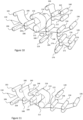
- Figure 10 illustrates an example embodiment of the latter option. Elements and stages that were shown and explained in Figure 5 are denoted in Figure 10 with same reference numbers and are not described with this drawing again. Further details on these elements can be referred from the description of any of the previous Figures.
- the layer of the carrier binding adhesive is a PSA tape 162 that it is rolled from the reel 120 onto the first carrier layer 122 and binds the top surfaces of the one or more conductive elements to the first carrier layer before the sacrificial substrate layer removing stage.
- Figure 10 shows an implementation where the roll-to-roll processing method includes a component 180 for a pre-releasing stage wherein the initial adhesive force of the releasably binding adhesive is reduced.
- the component 180 is shown in a position after the cutting tool 112 and after the recessed web 114 has been removed.
- the component 180 may be alternatively arranged to a position where it acts upon the roll-to-roll processed web after the cutting tool 112 but before the recessed web 114 is removed.
- Such component may be, for example, a source of ultraviolet light, but some other chemical or physical process (e.g. heating, use of a solvent) capable of reducing the adhesive force of an adhesive may be applied within the scope.
- the web to be rolled onto a transfer reel 136 includes a carrier layer (e.g. fabric, laminate layer, etc.) to which the conductive element is designed to remain adhesively bound.
- Figure 11 illustrates a further implementation wherein the method disclosed herein is used to create a layered web that enables transfer of large and fragile conductive elements onto a surface selected by the user on site without creating considerable profiles or intermediate top or bottom substrate layers onto the surface. Concrete examples of such use cases include retrofitting large but thin electrical components on 3D formed windmill blades or on planar surfaces like interior walls or floors of buildings. Elements and stages that were shown and explained in Figure 3 are denoted in Figure 11 with same reference numbers and are not described with this drawing again, further details on these elements can be referred from the description of, for example, Figures 1 and 3 .
- boundaries of one or more conductive elements are patterned into a layered web that includes a conducting layer 100 bound to a first substrate layer 104 with a first adhesive.
- the first substrate layer 104 is a protective film that can remain attached to the one or more conductive elements until they are transferred to a target surface.
- the first substrate layer is a transparent polymer film so that the one or more conductive elements can be accurately positioned when they are transferred to the target surface.
- the first adhesive is a releasably binding adhesive, which may be deposited on the first substrate layer in the process, as shown in Figure 11 , or may be readily provided on the polymer film with a protective sheet that is reeled off before the first substrate layer 104 is fed into the process.
- the conducting layer 100 is rolled out of one reel 102 and the first substrate layer 104 is rolled out of another reel 106 and the layers are pressed on each other with nip rolls 108.
- the layers 100, 104 can be laminated to each other in beforehand, and fed to the roll-to-roll process in a readily laminated form.
- a layer of the second adhesive is formed on the layered web before the patterning stage. Furthermore, after the patterning stage where boundaries of the conductive elements are patterned into the layered web but before the removing stage where the parts of the conducting layer outside the boundaries of the one or more conductive elements are removed from the first substrate layer, top surfaces of the one or more conductive elements are bound to the second substrate layer by activating adhesion of the second adhesive.
- An advantageous method to implement this is to use roll-to-roll transferable pressure sensitive adhesive (PSA) tape as the carrier binding adhesive.
- PSA pressure sensitive adhesive
- the constitution and form of a tape enables patterning of the second adhesive with patterning of the conductive elements.
- a PSA tape may need to be covered with a release liner, like a silicone covered polymer film.
- Figure 11 shows an implementation where the roll-to-roll process includes a further PSA reel 140 from which a PSA tape 142, which includes a layer of PSA material covered with a release liner is rolled on the layered sheet that rolls out of the nip rolls 108.
- the PSA tape is oriented so that the layer of PSA material gets into contact with the conducting layer of the layered web and the release liner is on the top.
- the layered web and the PSA tape are pressed together with nip rolls 144, which activates the PSA material, and forms the strong adhesion to the conducting layer in the layered web.
- the release liner can then be removed as a continuous sheet with a reel 146, as shown in Figure 11 .
- the PSA material now forms the carrier binding adhesive, covers the conducting layer, and becomes patterned with it in the cutting tool 112. Parts of the PSA material layer become also removed from the process with the removable parts of the conducting layer when the recessed web is released from the sacrificial substrate layer by means of the reel 116.
- the roll-to-roll processed web includes the first substrate layer and the conductive elements. Bottom surfaces of the conductive elements are bound to the first substrate layer with the first adhesive, and top surfaces of the conductive elements are covered with a piece of PSA material.
- the top surfaces of the conductive elements become strongly fixed to the second substrate layer 122.
- the first substrate layer 104 and the second substrate layer 122 are both formed of a transparent polymer film so that the one or more conductive elements can be accurately positioned when they are transferred to a selected target surface.
- the cutting tool 112 cuts the conductive elements and the second adhesive into a same patterned form.
- the second adhesive that bonds the top surfaces of the conductive elements in this example is thus a piece of pressure sensitive adhesive with a patterned form that is equal and aligned to the form of the patterned conductive element.
- Parts of the second substrate layer between the conductive elements are not covered by the second releasably binding adhesive. This means that the resulting layered web does not include parts where two adhesive layers would be glued to each other.
- the process may optionally include a further pair of nip rolls 134 to finalise the desired lamination and the final product that includes fragile conductive elements secured between the two protective substrate layers can then be rolled onto a transfer reel 136.
- Figure 12 shows an exploded view of layers of an exemplary dual-laminate product resulting from the exemplary roll-to-roll processing method described with Figure 11 .
- the layered web includes a first substrate layer 1200 covered with a thin layer of first adhesive 1202.
- the combination of the first substrate layer and the first adhesive may be provided by, for example, a silicone covered, transparent polymer film.
- the layered web also includes a conductive element 1204 and a piece of second adhesive 1206 with a patterned form that is equal and aligned to the patterned form of the patterned conductive element 1204.
- the topmost layer is the second substrate layer 1208.
- the second substrate layer 1208 is removed first.
- the first adhesive 1202 and the second adhesive 1206 are selected so that adhesion provided by the pattern of second adhesive 1206 between the top surfaces of the one or more conductive elements 1204 and the second substrate 1208 is weaker than adhesion provided by the first adhesive 1202 between bottom surfaces of the conductive elements 1204 and the first substrate layer 1200. Since the first and second adhesives are not in contact and the second adhesive 1206 covers only the conductive element 1204, the second substrate layer is easily removed from the layered web, and the first substrate layer 1200 further supports the fragile conductive element during the removal.
- the second adhesive 1206 remains attached to the conductive element 1204 and so the conductive element can be pressed on a target surface so that an adhesive bond is formed. Again, as the conductive element 1204 is attached to the target surface, it remains fully supported by the first substrate layer 1200 so even very large conductive elements that include very thin and thus easily wrinkling parts can be safely transferred on any surface. When the adhesive contact of the second adhesive has again been activated by pressing and smoothing the conductive element against the target surface, the first substrate layer 1200 can be pulled off so that only the conductive element remains attached to the target surface.
Landscapes
- Engineering & Computer Science (AREA)
- Microelectronics & Electronic Packaging (AREA)
- Manufacturing & Machinery (AREA)
- Mechanical Engineering (AREA)
- Laminated Bodies (AREA)
- Application Of Or Painting With Fluid Materials (AREA)
- Coating Apparatus (AREA)
- Manufacturing Of Printed Wiring (AREA)
Claims (7)
- Rolle-zu-Rolle-Bearbeitungsverfahren, umfassend:Gegenseitiges Verbinden (400) einer leitenden Schicht (100) und einer aus einem transparenten Polymerfilm ausgebildeten ersten Substratschicht (104, 1200) mit einem ersten Klebstoff (1202);Anbringen einer Schicht von zweitem Klebstoff (1206) auf der leitenden Schicht (100);Strukturieren (410) von Konturen eines oder mehrerer leitfähiger Elemente (900, 1204), wobei beim Strukturieren die Konturen durch die Schicht von zweitem Klebstoff (1206) und die leitende Schicht (100) hindurch, aber nicht durch die erste Substratschicht (104, 1200) hindurch geschnitten werden;Entfernen (420) von Teilen der leitenden Schicht (100) und Teilen der Schicht von zweitem Klebstoff (1206) außerhalb der Konturen des einen oder der mehreren leitfähigen Elemente (900, 1204) weg von der ersten Substratschicht (104, 1200);Verbinden (430) von oberseitigen Flächen des einen oder der mehreren leitfähigen Elemente (900, 1204) mit einer aus einem transparenten Polymerfilm ausgebildeten zweiten Substratschicht (122, 1208) mittels der Schicht von zweitem Klebstoff (1206), die in eine gleiche strukturierte Form wie eine strukturierte Form des einen oder der mehreren leitfähigen Elemente (900, 1204) strukturiert wird;Aufrollen (460) einer geschichteten Bahn (414) auf eine Spule, wobei die geschichtete Bahn das eine oder die mehreren leitfähigen Elemente (900, 1204) umfasst, die an der ersten Substratschicht (104, 1200) mit dem ersten Klebstoff (1202) und an der zweiten Substratschicht (122, 1208) mit der Schicht von zweitem Klebstoff (1206), angebracht sind, die in die gleiche strukturierte Form wie die strukturierte Form des einen oder mehreren leitfähigen Elemente (900, 1204) strukturiert wird.
- Verfahren nach Anspruch 1, gekennzeichnet dadurch, dass das Strukturieren umfasst: Kiss-Cutting oder Laserschneiden durch die leitende Schicht (100) und die Schicht von zweitem Klebstoff (1206) hindurch.
- Verfahren nach einem der vorhergehenden Ansprüche, gekennzeichnet dadurch, dass die leitende Schicht (100) eine Schicht von leitfähigem Metall und eine Polymerschicht umfasst.
- Verfahren nach einem der Ansprüche 1 bis 3, gekennzeichnet durch Entfernen (440) der Teile der leitenden Schicht (100) und der Teile des zweiten Klebstoffs (1206) durch Abziehen dieser Teile von der ersten Substratschicht (104, 1200) mit einer Kraft, die das Haftvermögen des ersten Klebstoffs (1202) übersteigt.
- Verfahren nach einem der vorhergehenden Ansprüche, gekennzeichnet durch Strukturieren (410) der Konturen des einen oder der mehreren leitfähigen Elemente (900, 1204) durch die leitende Schicht (100) und durch die Schicht von zweitem Klebstoff (1206) hindurch, so dass Teile der leitenden Schicht (100) und der Schicht von zweitem Klebstoff (1206), die von der ersten Substratschicht (104, 1200) zu entfernen sind, eine ausgesparte Bahn (114, 422) ausbilden;
Aufrollen der ausgesparten Bahn (114, 422) auf eine Spule (116) eines ersten Rolle-zu-Rolle-Elements zur Bereitstellung der Kraft, die die Teile der leitenden Schicht (100) und der Schicht von zweitem Klebstoff (1206) von der ersten Substratschicht (104, 1200) abzieht. - Verfahren nach einem der vorhergehenden Ansprüche, gekennzeichnet durch Anordnen des ersten Klebstoffs (1202) und des zweiten Klebstoffs (1206) dergestalt, dass das vom zweiten Klebstoff (1206) bereitgestellte Haftvermögen zwischen den oberseitigen Flächen des einen oder der mehreren leitfähigen Elemente (900, 1204) und der zweiten Substratschicht (122, 1208) schwächer ist als das vom ersten Klebstoff (1202) bereitgestellte Haftvermögen zwischen den unterseitigen Flächen des einen oder der mehreren leitfähigen Elemente und der ersten Substratschicht (104, 1200).
- Verfahren nach einem der vorhergehenden Ansprüche, gekennzeichnet dadurch, dass die Schicht von zweitem Klebstoff (1206) aus einem drucksensitiven Klebstoff ausgebildet wird.
Applications Claiming Priority (2)
| Application Number | Priority Date | Filing Date | Title |
|---|---|---|---|
| FI20215517A FI130466B (en) | 2021-05-04 | 2021-05-04 | IMPROVED ROLL-TO-ROLL PROCESS METHOD |
| PCT/FI2022/050291 WO2022234189A1 (en) | 2021-05-04 | 2022-05-03 | An improved roll-to-roll processing method and an object |
Publications (3)
| Publication Number | Publication Date |
|---|---|
| EP4334133A1 EP4334133A1 (de) | 2024-03-13 |
| EP4334133B1 true EP4334133B1 (de) | 2025-02-12 |
| EP4334133C0 EP4334133C0 (de) | 2025-02-12 |
Family
ID=81927887
Family Applications (1)
| Application Number | Title | Priority Date | Filing Date |
|---|---|---|---|
| EP22727355.4A Active EP4334133B1 (de) | 2021-05-04 | 2022-05-03 | Verbessertes roll-to-roll-verarbeitungsverfahren |
Country Status (9)
| Country | Link |
|---|---|
| US (1) | US20240227378A1 (de) |
| EP (1) | EP4334133B1 (de) |
| CN (1) | CN117255747A (de) |
| CA (1) | CA3217411A1 (de) |
| ES (1) | ES3014199T3 (de) |
| FI (1) | FI130466B (de) |
| MX (1) | MX2023013006A (de) |
| PL (1) | PL4334133T3 (de) |
| WO (1) | WO2022234189A1 (de) |
Families Citing this family (3)
| Publication number | Priority date | Publication date | Assignee | Title |
|---|---|---|---|---|
| US20240328637A1 (en) | 2023-04-03 | 2024-10-03 | The Warming Surfaces Company Oy | Method to create a microclimate and a microclimate creating heating system |
| WO2024209130A1 (en) | 2023-04-03 | 2024-10-10 | The Warming Surfaces Company Oy | Heat emission control in radiator heater matrix |
| FI20236357A1 (en) | 2023-12-11 | 2025-06-12 | Teknologian Tutkimuskeskus Vtt Oy | Battery or battery cell with a heater |
Citations (9)
| Publication number | Priority date | Publication date | Assignee | Title |
|---|---|---|---|---|
| US4091125A (en) * | 1976-11-08 | 1978-05-23 | Delgadillo Joseph A | Circuit board and method for producing same |
| US5645932A (en) * | 1993-12-30 | 1997-07-08 | Kabushiki Kaisha Miyake | Circuit-like metallic foil sheet and the like and process for producing them |
| US20060213609A1 (en) * | 2002-01-18 | 2006-09-28 | Alan Green | RFID label technique |
| US20070012775A1 (en) * | 2004-02-23 | 2007-01-18 | Checkpoint Systems, Inc. | Method of fabricating a security tag in an integrated surface processing system |
| DE102009033510A1 (de) * | 2008-11-13 | 2010-05-20 | Sefar Ag | Gewebe, Vorrichtung mit Gewebe sowie Herstellungsverfahren für Gewebe |
| US20130032283A1 (en) * | 2011-08-03 | 2013-02-07 | Graphic Packaging International, Inc. | Systems and Methods for Forming Laminates with Patterned Microwave Energy Interactive Material |
| US20140338739A1 (en) * | 2011-10-31 | 2014-11-20 | E I Du Pont De Nemours And Company | Integrated back-sheet for back contact photovoltaic module |
| US9307650B2 (en) * | 2009-06-29 | 2016-04-05 | Solarworld Industries Thueringen Gmbh | Method for manufacturing a foil-like electrical connector for connecting solar cells |
| US10842025B1 (en) * | 2019-09-20 | 2020-11-17 | Manaflex Llc | Reel-to-reel slug removal methods and devices in FPC fabrication |
Family Cites Families (8)
| Publication number | Priority date | Publication date | Assignee | Title |
|---|---|---|---|---|
| GB1411799A (en) * | 1972-12-08 | 1975-10-29 | Fortin Laminating Corp | Laminates of electrically conducting and insulating material |
| JP2002503008A (ja) * | 1998-02-06 | 2002-01-29 | フレクスコン カンパニー インク | 薄型フィルム状の貼着可能な電気素子 |
| DE60001045T2 (de) * | 2000-03-02 | 2003-09-04 | Gerber Scientific Products, Inc. | Verfahren und Vorrichtung zur Herstellung eines graphischen Produkts |
| WO2007001977A2 (en) * | 2005-06-20 | 2007-01-04 | Microcontinuum, Inc. | Systems and methods for roll-to-roll patterning |
| US8786510B2 (en) * | 2006-01-24 | 2014-07-22 | Avery Dennison Corporation | Radio frequency (RF) antenna containing element and methods of making the same |
| US7497004B2 (en) * | 2006-04-10 | 2009-03-03 | Checkpoint Systems, Inc. | Process for making UHF antennas for EAS and RFID tags and antennas made thereby |
| JP5042305B2 (ja) * | 2008-12-22 | 2012-10-03 | 株式会社フジクラ | フィルムアンテナ及びその製造方法 |
| FR3037966B1 (fr) * | 2015-06-24 | 2019-08-16 | Novacel | Film adhesif sensible a la pression et son utilisation pour la protection de surfaces |
-
2021
- 2021-05-04 FI FI20215517A patent/FI130466B/en active IP Right Grant
-
2022
- 2022-05-03 CA CA3217411A patent/CA3217411A1/en active Pending
- 2022-05-03 EP EP22727355.4A patent/EP4334133B1/de active Active
- 2022-05-03 CN CN202280032203.1A patent/CN117255747A/zh active Pending
- 2022-05-03 US US18/558,915 patent/US20240227378A1/en active Pending
- 2022-05-03 ES ES22727355T patent/ES3014199T3/es active Active
- 2022-05-03 PL PL22727355.4T patent/PL4334133T3/pl unknown
- 2022-05-03 WO PCT/FI2022/050291 patent/WO2022234189A1/en not_active Ceased
- 2022-05-03 MX MX2023013006A patent/MX2023013006A/es unknown
Patent Citations (9)
| Publication number | Priority date | Publication date | Assignee | Title |
|---|---|---|---|---|
| US4091125A (en) * | 1976-11-08 | 1978-05-23 | Delgadillo Joseph A | Circuit board and method for producing same |
| US5645932A (en) * | 1993-12-30 | 1997-07-08 | Kabushiki Kaisha Miyake | Circuit-like metallic foil sheet and the like and process for producing them |
| US20060213609A1 (en) * | 2002-01-18 | 2006-09-28 | Alan Green | RFID label technique |
| US20070012775A1 (en) * | 2004-02-23 | 2007-01-18 | Checkpoint Systems, Inc. | Method of fabricating a security tag in an integrated surface processing system |
| DE102009033510A1 (de) * | 2008-11-13 | 2010-05-20 | Sefar Ag | Gewebe, Vorrichtung mit Gewebe sowie Herstellungsverfahren für Gewebe |
| US9307650B2 (en) * | 2009-06-29 | 2016-04-05 | Solarworld Industries Thueringen Gmbh | Method for manufacturing a foil-like electrical connector for connecting solar cells |
| US20130032283A1 (en) * | 2011-08-03 | 2013-02-07 | Graphic Packaging International, Inc. | Systems and Methods for Forming Laminates with Patterned Microwave Energy Interactive Material |
| US20140338739A1 (en) * | 2011-10-31 | 2014-11-20 | E I Du Pont De Nemours And Company | Integrated back-sheet for back contact photovoltaic module |
| US10842025B1 (en) * | 2019-09-20 | 2020-11-17 | Manaflex Llc | Reel-to-reel slug removal methods and devices in FPC fabrication |
Also Published As
| Publication number | Publication date |
|---|---|
| US20240227378A1 (en) | 2024-07-11 |
| CA3217411A1 (en) | 2022-11-10 |
| FI20215517A1 (en) | 2022-11-05 |
| CN117255747A (zh) | 2023-12-19 |
| PL4334133T3 (pl) | 2025-06-09 |
| WO2022234189A1 (en) | 2022-11-10 |
| MX2023013006A (es) | 2023-11-15 |
| EP4334133C0 (de) | 2025-02-12 |
| FI130466B (en) | 2023-09-19 |
| ES3014199T3 (en) | 2025-04-21 |
| EP4334133A1 (de) | 2024-03-13 |
Similar Documents
| Publication | Publication Date | Title |
|---|---|---|
| EP4334133B1 (de) | Verbessertes roll-to-roll-verarbeitungsverfahren | |
| CA2648825C (en) | Process for making uhf antennas for eas and rfid tags and antennas made thereby | |
| US8745852B2 (en) | Method of making a self-adhering RFID antenna | |
| JP5260295B2 (ja) | 穴あき再帰性反射トリムの製造方法 | |
| WO2001054058A1 (en) | Method to manufacture a smart label inlet web and a smart label inlet web | |
| TW200920809A (en) | Double-faced pressure-sensitive adhesive sheet | |
| HK40109930A (en) | Improved roll-to-roll processing method | |
| HK40109930B (en) | Improved roll-to-roll processing method | |
| KR101718855B1 (ko) | 전자파 차폐 및 방열용 복합 시트의 제조 방법 | |
| KR100970662B1 (ko) | 의류용 하프커팅형 스탬핑호일 및 그 제조방법 | |
| JP6422586B2 (ja) | プリント配線板の製造方法ならびに該方法に用いられるプリント配線板保護フィルムおよびシート状積層体 | |
| JP4270800B2 (ja) | 粘着シートの製造方法 | |
| TR2023014196T2 (tr) | Geli̇şti̇ri̇lmi̇ş bi̇r rulodan ruloya i̇şleme yöntemi̇ | |
| JP2015140384A (ja) | テープロール体およびテープロール体の製造方法 | |
| CN112836782B (zh) | 一种射频标签及其制造方法 | |
| CN111275154A (zh) | 全模切的超高频电子标签天线及其加工设备和加工工艺 | |
| CN212471802U (zh) | 一种涂布模切机 | |
| US9981398B2 (en) | Transfer/punching process | |
| JP4692317B2 (ja) | 粘着基板、回路基板の製造方法および回路板 | |
| JP3164655B2 (ja) | 粘着体転写方法 | |
| KR100423581B1 (ko) | 가열 없이 라미네이트 가능한 경질 코팅층 및 감압접착층을 갖는 라미네이트 시트 | |
| JP2015064528A (ja) | ラベル連続体、その加工装置およびその加工方法 |
Legal Events
| Date | Code | Title | Description |
|---|---|---|---|
| STAA | Information on the status of an ep patent application or granted ep patent |
Free format text: STATUS: UNKNOWN |
|
| STAA | Information on the status of an ep patent application or granted ep patent |
Free format text: STATUS: THE INTERNATIONAL PUBLICATION HAS BEEN MADE |
|
| PUAI | Public reference made under article 153(3) epc to a published international application that has entered the european phase |
Free format text: ORIGINAL CODE: 0009012 |
|
| STAA | Information on the status of an ep patent application or granted ep patent |
Free format text: STATUS: REQUEST FOR EXAMINATION WAS MADE |
|
| 17P | Request for examination filed |
Effective date: 20231123 |
|
| AK | Designated contracting states |
Kind code of ref document: A1 Designated state(s): AL AT BE BG CH CY CZ DE DK EE ES FI FR GB GR HR HU IE IS IT LI LT LU LV MC MK MT NL NO PL PT RO RS SE SI SK SM TR |
|
| DAV | Request for validation of the european patent (deleted) | ||
| DAX | Request for extension of the european patent (deleted) | ||
| GRAP | Despatch of communication of intention to grant a patent |
Free format text: ORIGINAL CODE: EPIDOSNIGR1 |
|
| STAA | Information on the status of an ep patent application or granted ep patent |
Free format text: STATUS: GRANT OF PATENT IS INTENDED |
|
| RIC1 | Information provided on ipc code assigned before grant |
Ipc: H05K 3/04 20060101ALI20240821BHEP Ipc: B32B 37/20 20060101ALI20240821BHEP Ipc: B32B 37/12 20060101AFI20240821BHEP |
|
| INTG | Intention to grant announced |
Effective date: 20240910 |
|
| REG | Reference to a national code |
Ref country code: HK Ref legal event code: DE Ref document number: 40109930 Country of ref document: HK |
|
| GRAS | Grant fee paid |
Free format text: ORIGINAL CODE: EPIDOSNIGR3 |
|
| GRAA | (expected) grant |
Free format text: ORIGINAL CODE: 0009210 |
|
| STAA | Information on the status of an ep patent application or granted ep patent |
Free format text: STATUS: THE PATENT HAS BEEN GRANTED |
|
| AK | Designated contracting states |
Kind code of ref document: B1 Designated state(s): AL AT BE BG CH CY CZ DE DK EE ES FI FR GB GR HR HU IE IS IT LI LT LU LV MC MK MT NL NO PL PT RO RS SE SI SK SM TR |
|
| RAP3 | Party data changed (applicant data changed or rights of an application transferred) |
Owner name: THE WARMING SURFACES COMPANY OY |
|
| REG | Reference to a national code |
Ref country code: GB Ref legal event code: FG4D |
|
| REG | Reference to a national code |
Ref country code: CH Ref legal event code: EP |
|
| REG | Reference to a national code |
Ref country code: DE Ref legal event code: R096 Ref document number: 602022010555 Country of ref document: DE |
|
| REG | Reference to a national code |
Ref country code: IE Ref legal event code: FG4D |
|
| U01 | Request for unitary effect filed |
Effective date: 20250311 |
|
| REG | Reference to a national code |
Ref country code: ES Ref legal event code: FG2A Ref document number: 3014199 Country of ref document: ES Kind code of ref document: T3 Effective date: 20250421 |
|
| U07 | Unitary effect registered |
Designated state(s): AT BE BG DE DK EE FI FR IT LT LU LV MT NL PT RO SE SI Effective date: 20250319 |
|
| PG25 | Lapsed in a contracting state [announced via postgrant information from national office to epo] |
Ref country code: RS Free format text: LAPSE BECAUSE OF FAILURE TO SUBMIT A TRANSLATION OF THE DESCRIPTION OR TO PAY THE FEE WITHIN THE PRESCRIBED TIME-LIMIT Effective date: 20250512 |
|
| PGFP | Annual fee paid to national office [announced via postgrant information from national office to epo] |
Ref country code: PL Payment date: 20250509 Year of fee payment: 4 |
|
| U20 | Renewal fee for the european patent with unitary effect paid |
Year of fee payment: 4 Effective date: 20250605 |
|
| PGFP | Annual fee paid to national office [announced via postgrant information from national office to epo] |
Ref country code: ES Payment date: 20250611 Year of fee payment: 4 |
|
| PG25 | Lapsed in a contracting state [announced via postgrant information from national office to epo] |
Ref country code: IS Free format text: LAPSE BECAUSE OF FAILURE TO SUBMIT A TRANSLATION OF THE DESCRIPTION OR TO PAY THE FEE WITHIN THE PRESCRIBED TIME-LIMIT Effective date: 20250612 |
|
| PGFP | Annual fee paid to national office [announced via postgrant information from national office to epo] |
Ref country code: NO Payment date: 20250519 Year of fee payment: 4 |
|
| PG25 | Lapsed in a contracting state [announced via postgrant information from national office to epo] |
Ref country code: HR Free format text: LAPSE BECAUSE OF FAILURE TO SUBMIT A TRANSLATION OF THE DESCRIPTION OR TO PAY THE FEE WITHIN THE PRESCRIBED TIME-LIMIT Effective date: 20250212 |
|
| PG25 | Lapsed in a contracting state [announced via postgrant information from national office to epo] |
Ref country code: GR Free format text: LAPSE BECAUSE OF FAILURE TO SUBMIT A TRANSLATION OF THE DESCRIPTION OR TO PAY THE FEE WITHIN THE PRESCRIBED TIME-LIMIT Effective date: 20250513 |
|
| PGFP | Annual fee paid to national office [announced via postgrant information from national office to epo] |
Ref country code: TR Payment date: 20250429 Year of fee payment: 4 |
|
| PG25 | Lapsed in a contracting state [announced via postgrant information from national office to epo] |
Ref country code: SM Free format text: LAPSE BECAUSE OF FAILURE TO SUBMIT A TRANSLATION OF THE DESCRIPTION OR TO PAY THE FEE WITHIN THE PRESCRIBED TIME-LIMIT Effective date: 20250212 |
|
| PG25 | Lapsed in a contracting state [announced via postgrant information from national office to epo] |
Ref country code: CZ Free format text: LAPSE BECAUSE OF FAILURE TO SUBMIT A TRANSLATION OF THE DESCRIPTION OR TO PAY THE FEE WITHIN THE PRESCRIBED TIME-LIMIT Effective date: 20250212 |
|
| PG25 | Lapsed in a contracting state [announced via postgrant information from national office to epo] |
Ref country code: SK Free format text: LAPSE BECAUSE OF FAILURE TO SUBMIT A TRANSLATION OF THE DESCRIPTION OR TO PAY THE FEE WITHIN THE PRESCRIBED TIME-LIMIT Effective date: 20250212 |
|
| PLBE | No opposition filed within time limit |
Free format text: ORIGINAL CODE: 0009261 |
|
| STAA | Information on the status of an ep patent application or granted ep patent |
Free format text: STATUS: NO OPPOSITION FILED WITHIN TIME LIMIT |
|
| REG | Reference to a national code |
Ref country code: CH Ref legal event code: H13 Free format text: ST27 STATUS EVENT CODE: U-0-0-H10-H13 (AS PROVIDED BY THE NATIONAL OFFICE) Effective date: 20251223 |
|
| REG | Reference to a national code |
Ref country code: CH Ref legal event code: L10 Free format text: ST27 STATUS EVENT CODE: U-0-0-L10-L00 (AS PROVIDED BY THE NATIONAL OFFICE) Effective date: 20251224 |
|
| PG25 | Lapsed in a contracting state [announced via postgrant information from national office to epo] |
Ref country code: CH Free format text: LAPSE BECAUSE OF NON-PAYMENT OF DUE FEES Effective date: 20250531 |
|
| 26N | No opposition filed |
Effective date: 20251113 |
|
| PG25 | Lapsed in a contracting state [announced via postgrant information from national office to epo] |
Ref country code: MC Free format text: LAPSE BECAUSE OF FAILURE TO SUBMIT A TRANSLATION OF THE DESCRIPTION OR TO PAY THE FEE WITHIN THE PRESCRIBED TIME-LIMIT Effective date: 20250212 |