EP4322232A2 - Lichtemittierende vorrichtung - Google Patents
Lichtemittierende vorrichtung Download PDFInfo
- Publication number
- EP4322232A2 EP4322232A2 EP23213174.8A EP23213174A EP4322232A2 EP 4322232 A2 EP4322232 A2 EP 4322232A2 EP 23213174 A EP23213174 A EP 23213174A EP 4322232 A2 EP4322232 A2 EP 4322232A2
- Authority
- EP
- European Patent Office
- Prior art keywords
- light emitting
- emitting group
- group
- electrode
- light
- Prior art date
- Legal status (The legal status is an assumption and is not a legal conclusion. Google has not performed a legal analysis and makes no representation as to the accuracy of the status listed.)
- Pending
Links
Images




Classifications
-
- H—ELECTRICITY
- H10—SEMICONDUCTOR DEVICES; ELECTRIC SOLID-STATE DEVICES NOT OTHERWISE PROVIDED FOR
- H10H—INORGANIC LIGHT-EMITTING SEMICONDUCTOR DEVICES HAVING POTENTIAL BARRIERS
- H10H20/00—Individual inorganic light-emitting semiconductor devices having potential barriers, e.g. light-emitting diodes [LED]
- H10H20/80—Constructional details
- H10H20/85—Packages
- H10H20/851—Wavelength conversion means
- H10H20/8511—Wavelength conversion means characterised by their material, e.g. binder
- H10H20/8512—Wavelength conversion materials
-
- H—ELECTRICITY
- H10—SEMICONDUCTOR DEVICES; ELECTRIC SOLID-STATE DEVICES NOT OTHERWISE PROVIDED FOR
- H10H—INORGANIC LIGHT-EMITTING SEMICONDUCTOR DEVICES HAVING POTENTIAL BARRIERS
- H10H20/00—Individual inorganic light-emitting semiconductor devices having potential barriers, e.g. light-emitting diodes [LED]
- H10H20/80—Constructional details
- H10H20/83—Electrodes
- H10H20/831—Electrodes characterised by their shape
-
- H—ELECTRICITY
- H10—SEMICONDUCTOR DEVICES; ELECTRIC SOLID-STATE DEVICES NOT OTHERWISE PROVIDED FOR
- H10H—INORGANIC LIGHT-EMITTING SEMICONDUCTOR DEVICES HAVING POTENTIAL BARRIERS
- H10H20/00—Individual inorganic light-emitting semiconductor devices having potential barriers, e.g. light-emitting diodes [LED]
- H10H20/80—Constructional details
- H10H20/83—Electrodes
- H10H20/831—Electrodes characterised by their shape
- H10H20/8312—Electrodes characterised by their shape extending at least partially through the bodies
-
- H—ELECTRICITY
- H10—SEMICONDUCTOR DEVICES; ELECTRIC SOLID-STATE DEVICES NOT OTHERWISE PROVIDED FOR
- H10H—INORGANIC LIGHT-EMITTING SEMICONDUCTOR DEVICES HAVING POTENTIAL BARRIERS
- H10H20/00—Individual inorganic light-emitting semiconductor devices having potential barriers, e.g. light-emitting diodes [LED]
- H10H20/80—Constructional details
- H10H20/85—Packages
- H10H20/851—Wavelength conversion means
- H10H20/8511—Wavelength conversion means characterised by their material, e.g. binder
- H10H20/8512—Wavelength conversion materials
- H10H20/8513—Wavelength conversion materials having two or more wavelength conversion materials
-
- H—ELECTRICITY
- H10—SEMICONDUCTOR DEVICES; ELECTRIC SOLID-STATE DEVICES NOT OTHERWISE PROVIDED FOR
- H10W—GENERIC PACKAGES, INTERCONNECTIONS, CONNECTORS OR OTHER CONSTRUCTIONAL DETAILS OF DEVICES COVERED BY CLASS H10
- H10W90/00—Package configurations
-
- F—MECHANICAL ENGINEERING; LIGHTING; HEATING; WEAPONS; BLASTING
- F21—LIGHTING
- F21S—NON-PORTABLE LIGHTING DEVICES; SYSTEMS THEREOF; VEHICLE LIGHTING DEVICES SPECIALLY ADAPTED FOR VEHICLE EXTERIORS
- F21S10/00—Lighting devices or systems producing a varying lighting effect
-
- F—MECHANICAL ENGINEERING; LIGHTING; HEATING; WEAPONS; BLASTING
- F21—LIGHTING
- F21Y—INDEXING SCHEME ASSOCIATED WITH SUBCLASSES F21K, F21L, F21S and F21V, RELATING TO THE FORM OR THE KIND OF THE LIGHT SOURCES OR OF THE COLOUR OF THE LIGHT EMITTED
- F21Y2105/00—Planar light sources
- F21Y2105/10—Planar light sources comprising a two-dimensional [2D] array of point-like light-generating elements
- F21Y2105/14—Planar light sources comprising a two-dimensional [2D] array of point-like light-generating elements characterised by the overall shape of the two-dimensional [2D] array
- F21Y2105/18—Planar light sources comprising a two-dimensional [2D] array of point-like light-generating elements characterised by the overall shape of the two-dimensional [2D] array annular; polygonal other than square or rectangular, e.g. for spotlights or for generating an axially symmetrical light beam
-
- F—MECHANICAL ENGINEERING; LIGHTING; HEATING; WEAPONS; BLASTING
- F21—LIGHTING
- F21Y—INDEXING SCHEME ASSOCIATED WITH SUBCLASSES F21K, F21L, F21S and F21V, RELATING TO THE FORM OR THE KIND OF THE LIGHT SOURCES OR OF THE COLOUR OF THE LIGHT EMITTED
- F21Y2113/00—Combination of light sources
- F21Y2113/10—Combination of light sources of different colours
- F21Y2113/13—Combination of light sources of different colours comprising an assembly of point-like light sources
- F21Y2113/17—Combination of light sources of different colours comprising an assembly of point-like light sources forming a single encapsulated light source
-
- F—MECHANICAL ENGINEERING; LIGHTING; HEATING; WEAPONS; BLASTING
- F21—LIGHTING
- F21Y—INDEXING SCHEME ASSOCIATED WITH SUBCLASSES F21K, F21L, F21S and F21V, RELATING TO THE FORM OR THE KIND OF THE LIGHT SOURCES OR OF THE COLOUR OF THE LIGHT EMITTED
- F21Y2115/00—Light-generating elements of semiconductor light sources
- F21Y2115/10—Light-emitting diodes [LED]
-
- H—ELECTRICITY
- H10—SEMICONDUCTOR DEVICES; ELECTRIC SOLID-STATE DEVICES NOT OTHERWISE PROVIDED FOR
- H10H—INORGANIC LIGHT-EMITTING SEMICONDUCTOR DEVICES HAVING POTENTIAL BARRIERS
- H10H20/00—Individual inorganic light-emitting semiconductor devices having potential barriers, e.g. light-emitting diodes [LED]
- H10H20/80—Constructional details
- H10H20/85—Packages
- H10H20/857—Interconnections, e.g. lead-frames, bond wires or solder balls
Definitions
- the present disclosure relates to a light emitting device, and more particularly, to a light emitting device which can be used in a lighting fixture using a light emitting diode as a light source.
- cortisol hormone allows more blood to be supplied to each organ of the body to counteract external stimuli such as stress, as a result, pulses and respiration are increased and the human body is awakened from sleep to prepare for outside activities.
- physical activities are performed under strong sunlight, but melatonin hormone is secreted in the evening and lowers pulse rate, body temperature, and blood pressure, as a result, gets a human body tired and helps to sleep.
- indoor lighting devices generally exhibit certain spectral power distributions, and these spectral power distributions have many differences from the spectral power distribution of sunlight.
- a light emitting device using blue, green, and red light emitting diodes even though white light can be implemented by a combination of blue, green, and red, the light emitting device does not exhibit a spectral power distribution over a wide wavelength range of visible range as in sunlight, but exhibit a distribution having a peak at a certain wavelength
- human skin produces vitamin D using ultraviolet rays of sunlight, but indoor lighting devices do not have these ultraviolet components and vitamin D is not produced even if activities are done under indoor lighting devices for a long period.
- Exemplary embodiments of the present disclosure provide a light emitting device to implement spectral power distribution change of sunlight which a human body is adapted to.
- exemplary embodiments of the present disclosure provide a light emitting device capable of implementing a desired spectral power distribution with spectral power of sunlight adapted to the human body.
- exemplary embodiments of the present disclosure provide a light emitting device illuminating indoor rooms and providing ultraviolet rays capable of producing vitamin D from human skin similarly to sunlight.
- a light emitting device in accordance with one exemplary embodiment comprises at least one main light emitting unit including a light emitting diode chip and a wavelength converter to emit white light, wherein the light emitting diode chip comprises an ultraviolet chip, a violet chip or a blue chip, and is adjustable to emit light corresponding to a spectral power distribution of morning sunlight, light corresponding to a spectral power distribution of afternoon sunlight, and light corresponding to a spectral power distribution of evening sunlight.
- a light emitting device in accordance with another exemplary embodiment comprises a base; a first electrode, a second electrode, a third electrode and a fourth electrode formed on the base; and a first light emitting group on the base and a second light emitting group disposed adjacent to the first light emitting group, wherein each of the first light emitting group and the second light emitting group comprises a plurality of light emitting diode chips, respectively, wherein the first light emitting group and the second light emitting group emit light of different color temperature, respectively, wherein the first light emitting group is connected to the first electrode and the third electrode, and wherein the second light emitting group is connected to the second electrode and the fourth electrode.
- the term "light emitting unit” indicates an individual light emitting source capable of implementing a specific spectral power distribution within a light emitting device.
- the light emitting diode chip becomes a light emitting unit
- the combination of the light emitting diode chip and the wavelength converter becomes a light emitting unit.
- a light emitting unit implementing white light by a combination of a light emitting diode chip and a wavelength converter is called a main light emitting unit
- a light emitting unit implementing light other than white light is called an auxiliary light emitting unit.
- FIG. 1 is a schematic cross-sectional view for illustrating a light emitting device in accordance with an exemplary embodiment of the present disclosure.
- the light emitting device may comprise a base 10, light emitting diode chips 20a, 20b, and 20c and wavelength converters 30a, 30b, and 30c.
- the base 10 may comprise circuit wirings for supplying electric power to each of the light emitting diode chips 20a, 20b, and 20c.
- Each of the light emitting diode chips 20a, 20b, and 20c may be a ultraviolet (UV) chip, a violet chip or a blue chip.
- the ultraviolet chip may emit light in the wavelength range of 290 to 390 nm, but is not particularly limited thereto.
- the ultraviolet chip may emit ultraviolet light in the wavelength range of 290 to 320 nm, as a result, it may contribute to the production of vitamin D from human skins.
- the violet chip may emit light in the range of 400 to 440 nm and the blue chip may emit light in the range of 440 to 470 nm.
- the light emitting diode chips 20a, 20b, and 20c may be chips having the same peak wavelength, but they are not limited thereto, and may emit light of different peak wavelengths within the above ranges.
- the wavelength converters 30a, 30b, and 30c may be coated or adhered onto the chips.
- the wavelength converters 30a, 30b, and 30c may comprise phosphors emitting fluorescence in relatively wide wavelength ranges.
- One or more phosphors may be incorporated in each of the wavelength converters 30a, 30b, and 30c.
- phosphors may comprise YAG phosphors, LuAG phosphors, ⁇ -sialon (SiAlON), alpha-sialon (SiAlON), CASN, Silicate BAM phosphors, or others, and at least one of these can be selected.
- YAG phosphor is generally selected for yellow wavelengths, and it is possible to emit light in a wavelength range from yellowish orange to green by adding Gd and Ga. As Gd is added and its amount increases, a wavelength shifts to a longer wavelength, while as Ga is added and its amount increases, a wavelength shifts to a shorter wavelength.
- LuAG-based phosphor is mainly selected for yellowish green wavelengths, and it is possible to emit Cyan color by adding Ga.
- Beta sialon (SiAlON) is suitable for emitting light in a green wavelength range
- alpha sialon (SiAlON) is suitable for emitting light in an amber wavelength range
- CASN CaAlSiN
- CASN CaAlSiN
- Light corresponding to a spectral power distribution of morning sunlight is implemented by the light emitting diode chip 20a and the wavelength converter 30a.
- light corresponding to a spectral power distribution of daylight is implemented by the light emitting diode chip 20b and the wavelength converter 30b
- light corresponding to a spectral power distribution of evening sunlight is implemented by the light emitting diode chip 20c and the wavelength converter 30c.
- a combination of the light emitting diode chip and the wavelength converter constitutes a "light emitting unit".
- the light emitting unit represents a unit capable of implementing a particular spectral power distribution individually in a light emitting device.
- a light emitting unit emitting white light is called a main light emitting unit
- a light emitting unit emitting light of a color other than white light is called an auxiliary light emitting unit. Therefore, light emitting units of this exemplary embodiment are all main light emitting
- light emitting units are illustrated as being mounted on a single base 10, light emitting units may be provided as light emitting modules mounted on different sub-mounts or printed circuit boards, and these light emitting modules may be mounted on the base 10.
- the light emitting units may be molded together by the same molding material, or molded respectively by molding materials which are separated from each other.
- the light emitting device may be used for various lighting devices such as light bulbs and tube lighting devices.
- each light emitting unit independently operates and implements light corresponding to morning sunlight, afternoon sunlight, or evening sunlight.
- FIG. 2 is a schematic cross-sectional view for illustrating a light emitting device in accordance with another exemplary embodiment of the present disclosure.
- the light emitting device in accordance with the present embodiment comprises a base 10, light emitting diode chips 20a and 20d, and a wavelength converter 30a.
- the light emitting diode chip 20a may be an ultraviolet (UV) chip, a violet chip or a blue chip.
- UV ultraviolet
- the blue chip can emit light in the range of 390 to 470 nm, in particular, it can emit light in the short wavelength range of 390 to 430 nm.
- the wavelength converter 30a comprises a phosphor, and the phosphor may be selected from the phosphors described in the previous embodiment.
- a light emitting unit (a main light emitting unit) including the light emitting diode chip 20a and the wavelength converter 30a may implement light corresponding to a spectral power distribution of morning sunlight, afternoon sunlight or evening sunlight, respectively, but is not limited thereto.
- the light emitting diode chip 20d is used for a light emitting unit without a wavelength converter.
- the light emitting diode chip 20d is an auxiliary light emitting unit, which may be selected from a violet chip, a blue chip, a cyan chip, a creen chip, a yellow chip, an amber chip, or a red chip.
- One of the chips among them may be selected and used, or a combination of two or more chips may be selected and used.
- light emitting units are illustrated as being mounted on the single base 10, light emitting units may be provided as light emitting modules mounted on different sub-mounts or printed circuit boards, and these light emitting modules may be mounted on the base 10.
- the main light emitting unit may emit light corresponding to a spectral power distribution of morning sunlight, afternoon sunlight, or evening sunlight, and light corresponding to spectral power distributions of two different sunlight may be implemented by combining the main light emitting unit and the auxiliary light emitting unit.
- light corresponding to each of spectral power distributions of morning sunlight, afternoon sunlight, and evening sunlight may be implemented by both of the main lighting unit and the auxiliary lighting unit.
- FIG. 3 is a schematic cross-sectional view for illustrating a light emitting device in accordance with another exemplary embodiment of the present disclosure.
- the base 10 comprises light emitting diode chips 20a and 20c and wavelength converters 30a and 30c.
- the light emitting diode chip 20a and the wavelength converter 30a constitute a main light emitting unit
- a light emitting diode chip 20e and a wavelength converter 30e constitute an auxiliary light emitting unit.
- the light emitting diode chip 20a may be an ultraviolet chip, a violet chip or a blue chip as described in previous embodiments.
- the light emitting diode chip 20e is a blue chip, and the wavelength converter 30e comprises at least one phosphor selected from cyan, green, yellow, amber, or red phosphor.
- auxiliary light emitting unit In the present exemplary embodiment, it is described that one auxiliary light emitting unit is used, but a plurality of auxiliary light emitting units may be used.
- the main light emitting unit may emit light corresponding to a spectral power distribution of morning sunlight, afternoon sunlight, or evening sunlight, and light corresponding to spectral power distributions of two different sunlight may be implemented by combining the main light emitting unit and the auxiliary light emitting unit.
- light corresponding to each of the spectral power distributions of morning sunlight, afternoon sunlight, and evening sunlight may be implemented by both of the main lighting unit and the auxiliary lighting unit.
- FIG. 4 is a schematic cross-sectional view for illustrating a light emitting device in accordance with another exemplary embodiment of the present disclosure.
- the light emitting device in accordance with the present exemplary embodiment comprises a base 10, light emitting diode chips 20a, 20d, and 20e, and wavelength converters 30a and 30e.
- the light emitting diode chip 20a and the wavelength converter 30a constitute a main light emitting unit
- the light emitting diode chip 20d constitutes a first auxiliary light emitting unit
- the light emitting diode chip 30e constitutes a second auxiliary light emitting unit.
- the light emitting diode chip 20a may be an ultraviolet chip, a violet chip or a blue chip as described in previous embodiments.
- the light emitting diode chip 20d may be selected from a violet chip, a blue chip, a cyan chip, a green chip, a yellow chip, an amber chip, or a red chip, or any combination thereof.
- the light emitting diode chip 20e is a blue chip as described in the embodiment of FIG. 3 , the wavelength converter 30e is at least one selected from cyan, green, yellow, amber, or red phosphors.
- a single or a plurality of auxiliary light emitting units including a light emitting diode chip 20e and a wavelength converter 30e may be used for the light emitting device in the present embodiment.
- the main light emitting unit may emit light corresponding to a spectral power distribution of morning sunlight, afternoon sunlight, or evening sunlight, and light corresponding to spectral power distributions of two different sunlight may be implemented by combining the main light emitting unit and the first and the second auxiliary light emitting units.
- light corresponding to each of the spectral power distributions of morning sunlight, afternoon sunlight, and evening sunlight may be implemented by combining the main light emitting unit and the first and/or the second auxiliary light emitting units.
- FIG. 5 is a schematic cross-sectional view for illustrating a light emitting device in accordance with another exemplary embodiment of the present disclosure.
- the light emitting device in accordance with the present exemplary embodiment comprises a base 10, light emitting diode chips 20a, 20b, and 20d, and wavelength converters 30a and 30b.
- the light emitting diode chips 20a and 20b may be ultraviolet chips, violet chips or blue chips as described above, and the light emitting diode chip 20d, as described in the embodiment of FIG. 2 , may be selected from a violet chip, a blue chip, a cyan chip, a green chip, a yellow chip, an amber chip, or a red chip, or any combination thereof.
- the wavelength converter 30a and 30b comprise phosphors as described in the embodiment of FIG. 1 .
- the light emitting diode chip 20a and the wavelength converter 30a constitute a first main light emitting unit
- the light emitting diode chip 20b and the wavelength converter 30b constitute a second main light emitting unit, which implement white respectively.
- the first light emitting unit may implement cool white
- the second light emitting unit may implement warm white.
- an auxiliary light emitting unit including the light emitting diode chip 20d emits light in the wavelength range of violet, blue, cyan, green, yellow, amber, or red.
- light corresponding to a spectral power distribution of morning sunlight, afternoon sunlight, or evening sunlight may be roughly implemented by a combination of the first light emitting unit and the second light emitting unit, and a spectral power distribution of sunlight may be precisely controlled by the auxiliary light emitting unit. Therefore, light corresponding to each of the spectral power distributions of morning sunlight, afternoon sunlight, and evening sunlight may be implemented by combining the first light emitting unit, the second light emitting unit and the auxiliary light emitting unit.
- FIG. 6 is a schematic cross-sectional view for illustrating a light emitting device in accordance with another exemplary embodiment of the present disclosure.
- the light emitting device in accordance with the present exemplary embodiment comprises a first light emitting unit and a second light emitting unit, similarly to the light emitting device described with reference to FIG. 5 .
- the auxiliary light emitting unit of Fig. 5 is replaced with the auxiliary light emitting unit described in the embodiment of FIG. 3 .
- the auxiliary light emitting unit comprises a light emitting diode chip 20e and a wavelength converter 30e
- the light emitting diode chip 20e is a blue chip
- the wavelength converter 30e comprises at least one of cyan, green, yellow, amber, or red phosphors.
- one auxiliary light emitting unit may be used, and a plurality of auxiliary light emitting units may be used.
- light corresponding to each of the spectral power distributions of morning sunlight, afternoon sunlight, and evening sunlight is implemented by combining the first light emitting unit, and the second light emitting unit and the auxiliary light emitting unit.
- FIG. 7 is a schematic cross-sectional view for illustrating a light emitting device in accordance with another exemplary embodiment of the present disclosure.
- the light emitting device in accordance with the present exemplary embodiment comprises a first light emitting unit, a second light emitting unit and an auxiliary light emitting unit, similarly to the light emitting device described with reference to FIG. 5 .
- the light emitting device in accordance with the present embodiment further comprises auxiliary light emitting units 20e and 30e described with reference to FIG. 6 .
- light corresponding to each of the spectral power distributions of morning sunlight, afternoon sunlight, and evening sunlight is implemented by combining the first light emitting unit, the second light emitting unit and the auxiliary light emitting unit.
- Light close to the wavelength distribution of sunlight may be implemented by comprising two kinds of auxiliary light emitting units.
- FIG. 8 is a schematic cross-sectional view for illustrating a light emitting device in accordance with another exemplary embodiment of the present disclosure.
- the light emitting device in accordance with the present embodiment is substantially similar to the light emitting diode described with reference to FIG.1 , but is different in that it further comprises an ultraviolet light emitting diode chip 20f.
- the ultraviolet light emitting diode chip 20f may emit ultraviolet rays having a wavelength within ranges of 290 to 320 nm, and as a result, it may be irradiated on human skins and vitamin D may be produced.
- the ultraviolet light emitting diode chip 20f may also be added to the embodiments of FIGs. 2 to 7 .
- the light emitting units may be molded together by the same molding material, or molded respectively by molding materials which are separated from each other.
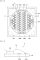
- FIG. 9 is a plan view for illustrating a light emitting device in accordance with another exemplary embodiment of the present disclosure.
- the light emitting device 100 in accordance with the exemplary embodiment may comprise a base 110, first to fourth light emitting groups L1, L2, L3, and L4, each of which comprises one or more light emitting diode chips 120, first to fourth electrode pads 131, 141, 151, and 161 and first to eighth electrode terminals 133, 135, 143, 145, 153, 155, 163, and 165.
- the light emitting diode chips 120 comprised in the light emitting groups L1, L2, L3 and L4 may be mounted on the base 110, such as a printed circuit board, and electric power may be provided to each of the light emitting groups L1, L2, L3, and L4, through the first to fourth electrode pads 131, 141, 151, and 161 and the first to eighth electrode terminals 133, 135, 143, 145, 153, 155, 163, and 165.
- Each of the first to fourth light emitting groups L1, L2, L3, and L4 may comprise one or more light emitting diode chips 120.
- the plurality of light emitting diode chips 120 may be electrically connected to one another within the light emitting groups L1, L2, L3, and L4, and the plurality of light emitting diode chips 120 may be connected in a serial connection or a parallel connection.
- the first to fourth light emitting groups L1, L2, L3, and L4 may independently emit light having a predetermined color temperature, respectively.
- light emitting diode chips 120 comprised in each of the light emitting groups L1, L2, L3, and L4 may be chips having the same peak wavelength.
- the present disclosure is not limited thereto, and it is possible to emit light having different peak wavelengths one another within a predetermined range.
- the first to fourth light emitting groups L1, L2, L3, and L4 may emit light having different color temperatures one another.
- two or more light emitting groups may emit light having the same color temperature, and remaining light emitting groups may emit light having other color temperature.
- the first light emitting group L1 and the third light emitting group L3 may emit light having the same color temperature
- the second light emitting group L2 and the fourth light emitting group L4 may emit light having the same color temperature.
- the color temperature of the light emitted from the first and third light emitting groups L1 and L3 and the color temperature of the light emitted from the second and fourth light emitting groups L2 and L4 may be different.
- the first to fourth light emitting groups L 1, L 2, L 3, and L 4 may comprise a wavelength converter comprising a phosphor as needed.
- the light emitting diode chips 120 comprised in the same light emitting group of the first to fourth light emitting groups L1, L2, L3, and L4 may be used to implement light emitting sources implementing the same spectral power distribution or may be used to implement light emitting sources implementing different spectral power distributions.
- a wavelength converter may be arranged on the light emitting diode chip 120, and a predetermined spectral power distribution may be shown.
- the wavelength converters may be independently disposed on the respective light emitting diode chips 120, but it is not limited thereto, and the wavelength converters may be disposed to cover the respective light emitting groups L1, L2, L3, and L4.
- the main light emitting unit and / or auxiliary light emitting unit described in the previous embodiments 1 to 8 may be formed.
- light emitting diode chips 120 comprised in each of the light emitting groups L1, L2, L3, and L4 may implement main light emitting units or auxiliary light emitting units together with a wavelength converter, thus, the light emitting device 100 may change spectral power distributions of light corresponding to power of sunlight and in accordance with changes in spectral power distributions of sunlight.
- the light emitting diode chips 120 comprised in each of light emitting groups L1, L2, L3, and L4 may emit light having different wavelengths, for example, a blue light emitting diode chip, a green light emitting diode chip, and a red light emitting diode chip may be used in one light emitting group, and light emitted from each light emitting diode chip 120 may be mixed and emit white light.
- the main light emitting unit and the auxiliary light emitting unit may be comprised in each light emitting group.
- the plurality of light emitting diode chips 120 comprised in each of the light emitting groups L1, L2, L3, and L4 serve as light emitting sources, respectively.
- the plurality of light emitting diode chips 120 may be alternately arranged on the bases 110. Alternatively in the case when blue light emitting diode chips, green light emitting diode chips and red light emitting diode chips are used, they may be arranged concentrically adjacent to each other or triangularly arranged.
- 20 light emitting diode chips 120 are comprised in each of the first to fourth light emitting groups L1, L2, L3, and L4, and it is described and illustrated that the first to fourth light emitting groups L1, L2, L3, and L4 are disposed in a circular mounting portion on the base 110.
- 20 light emitting diode chips 120 comprised in the first light emitting group L1 may be arranged in three lines, and a plurality of light emitting diode chips 120 in each line may be arranged at predetermined distances.
- a light emitting diode chip 120 arranged in each line may not be arranged to be flush with a light emitting diode chip 120 of an adjacent line thereto, but may be arranged in a position shifted upward or downward.
- the light emitting diode chips 120 arranged in each line may be arranged at the same distance from one another, and the light emitting diode chip 120 arranged in one line may be arranged to be flush with a center between two light emitting diode chips 120 of an adjacent line thereto.
- the first light emitting group L1 may be configured in three lines comprising three light emitting diode chips 120, eight light emitting diode chips 120 and nine light emitting diode chips 120, respectively, and the light emitting diode chips 120 of the respective lines may be arranged alternately with one another.
- light emitting units of a same kind may be arranged to be spaced apart at a distance and not to be adjacent to one another, and may implement uniform light.
- 20 light emitting diode chips 120 comprised in the second light emitting group L2 may be arranged in two lines, and 10 light emitting diode chips 120 may be arranged in each line at a predetermined distance.
- the light emitting diode chips 120 arranged in each line may not be arranged to be flush with a light emitting diode chip 120 of an adjacent line thereto, but may be arranged in a position shifted upward or downward.
- the light emitting diode chips 120 arranged in each line may be arranged at the same distance from one another, and the light emitting diode chip 120 arranged in one line may be arranged to be flush with a center between two light emitting diode chips 120 of an adjacent line thereto.
- 20 light emitting diode chips 120 may be arranged in two lines, and the light emitting diode chips 120 arranged in each line may not be arranged to be flush with a light emitting diode chip 120 of an adjacent line thereto, but may be arranged in a position shifted upward or downward.
- the light emitting diode chips 120 arranged in each line may be arranged at the same distance from one another, and the light emitting diode chip 120 arranged in one line may be arranged to be flush with a center between two light emitting diode chips 120 of an adjacent line thereto.
- the fourth light emitting group L4 similarly to the first light emitting group L1, may have 20 light emitting diode chips 120 arranged in three lines.
- the length of a wire W connecting each light emitting diode chip 120 may be minimized by arranging the plurality of light emitting diode chips 120 comprised in each of light emitting groups L1, L2, L3, and L4 at shifted positions. Further, as described above, even if the number of the light emitting diode chips 120 comprised in the light emitting device 100 is reduced, a desired color temperature may be implemented by arranging the plurality of light emitting diode chips 120.
- the light emitting diode chips 120 may be arranged in a densely packed state, and uniform light may be implemented. Blue, green, and red light emitting diode chips are described as examples, but it is not limited thereto, and three kinds of main light emitting units, or two kinds of main light emitting units and one auxiliary light emitting unit, or one main light emitting unit and two kinds of auxiliary light emitting units may be arranged as described above.
- the first to fourth electrode pads 131, 141, 151, and 161 are disposed at the four corners of the base 110, respectively, and are incorporated to electrically connect to an external power supply. To do this, the first to fourth electrode pads 131, 141, 151, and 161 may be formed to have predetermined widths.
- the first to eighth electrode terminals 133, 135, 143, 145, 153, 155, 163, and 165 may be incorporated to electrically connect to the first to fourth light emitting groups L1, L2, L3, and L4, respectively, the first to eighth electrode terminals 133, 135, 143, 145, 153, 155, 163, and 165 may be formed in a shape surrounding the first to fourth light emitting groups L 1, L 2, L 3, and L 4 in the present embodiment.
- the first light emitting group L1 is electrically connected to the second electrode terminal 135 and the sixth electrode terminal 155
- the second light emitting group L2 is electrically connected to the third electrode terminal 143 and the seventh electrode terminal 163.
- the third light emitting group L 3 is electrically connected to the first electrode terminal 133 and the fifth electrode terminal 153
- the fourth light emitting group L4 is electrically connected to the fourth electrode terminal 145 and the eighth electrode terminal 165.
- the first to fourth electrode terminals 133, 135, 143, and 145 may be terminals for supplying power to the first to fourth light emitting groups L1, L2, L3, and L4, and the fifth to eighth electrode terminals 153, 155, 163, and 165 may be ground terminals.
- the first electrode pad 131 and the second electrode pad 141 may be terminals for supplying power to the first to fourth light emitting groups L1, L2, L3, and L4
- the third electrode pad 151 and the fourth electrode pad 161 may be ground terminals.
- it is not limited thereto, and a type of each electrode terminal and electrode pad may be changed as required.
- a blue light emitting diode chip, a green light emitting diode chip and a red light emitting diode chip may be electrically connected to electrode pads in a state of being connected to a common terminal, and light emitting groups having different color temperatures of the first to fourth light emitting groups L1, L2, L3, and L4 may be also connected to a common terminal as in the present embodiment.
- a reflector D1 may be disposed to surround the first to fourth light emitting groups L1, L2, L3, and L4, and a partition wall D2 may be disposed among the first to fourth light emitting groups L1, L2, L3, and L4.
- the reflector D1 may define a light emitting surface of the light emitting device 100 by being disposed so as to surround the first to fourth light emitting groups L1, L2, L3, and L4, and may define an area for forming a molding portion Ph on the light emitting surface defined inside the reflector D1.
- the reflector D1 may reflect light emitted from the first to fourth light emitting groups L1, L2, L3, and L4 to improve a light emission efficiency of the light emitting device 100.
- the partition wall D2 is disposed among the first to fourth light emitting groups L1, L2, L3, and L4, and incorporated to prevent light emitted from each light emitting group L1, L2, L3 and L4 from being mixed with light emitted from the adjacent light emitting groups L1, L2, L3, and L4.
- FIG. 10 is a view for illustrating electrical connections between light emitting groups and electrodes of the light emitting device in accordance with the present embodiment
- FIG. 11 is a cross-sectional view of section A of Figure 10 .
- FIG. 10 is a view in which an insulating layer (not shown) covering the electrodes is removed from the base 110 in the light emitting device 100 of FIG. 9 , and electrode shapes forming the electrode pads and the electrode terminals are displayed as the insulating layer is removed. And in FIG. 10 , positions where each electrode pad and electrode terminal are arranged are indicated by dotted lines.
- a first electrode pad 131, a first electrode terminal 133 and a second electrode terminal 135 are formed as the insulating layer is formed on a first electrode 130, and a second electrode pad 141, a third electrode terminal 143 and a fourth electrode terminal 145 are formed as the insulating layer is formed on a second electrode 140.
- a third electrode pad 151, a fifth electrode terminal 153 and a sixth electrode terminal 155 are formed as the insulating layer is formed on a third electrode 150, and a fourth electrode pad 161, a seventh electrode terminal 163 and an eighth electrode terminal 165 are formed as the insulating layer is formed on a fourth electrode 160.
- first to fourth electrodes 130, 140, 150, and 160 may be formed with first to fourth electrode extensions 130a, 140a, 150a, and 160a on their sides, respectively.
- the first electrode extension 130a is formed extending from the first electrode 130 toward the second electrode 140
- the second electrode extension 140a is formed extending from the second electrode 140 toward the first electrode 130.
- the first electrode extension 130a and the second electrode extension 140a may have a region arranged so as to be adjacent to each other, but may be spaced apart so as to be electrically insulated from each other.
- the second electrode extension 140a may be arranged outside of the first electrode extension 130a relative to a position where the light emitting groups L1, L2, L3, and L4 are arranged.
- the third electrode extension 150a is formed extending from the third electrode 150 toward the fourth electrode 160
- the forth electrode extension 160a is formed extending from the fourth electrode 160 toward the third electrode 150.
- the third electrode extension 150a and the fourth electrode extension 160a may have a region arranged so as to be adjacent to each other, but may be spaced apart so as to be electrically insulated from each other.
- the fourth electrode extension 160a may be arranged outside of the third electrode extension 150a relative to a position where the light emitting groups L1, L2, L3, and L4 are arranged.
- the first light emitting group L1 is electrically connected to the first electrode 130 and the third electrode 150
- the second light emitting group L2 is electrically connected to the second electrode 140 and the fourth electrode 160
- the third light emitting group L3 is electrically connected to the first electrode 130 and the third electrode 150
- the fourth light emitting group L4 is electrically connected to the second electrode 140 and the fourth electrode portion 160.
- the first light emitting group L1 and the third light emitting group L3 may be simultaneously controlled and driven, and the second light emitting group L2 and the fourth light emitting group L4 may be simultaneously controlled and driven, but it is not limited thereto, and positions of simultaneously driven light emitting groups L1, L2, L3, and L4 may be changed.
- the first light emitting group L1 and the third light emitting group L3 may be configured to emit light at a color temperature of 1800 K
- the second light emitting group L2 and the fourth light emitting group L4 may be configured to emit light at a color temperature of 4000 K.
- light emitted from each light emitting group L1, L2, L3, and L4 may be mixed to emit light having a color temperature of about 3000 K based on operation of each light emitting group L1, L2, L3, and L4, and it is possible to change the light mixed in an adjustment of a light emitting power or the like of each light emitting group L1, L2, L3, and L4.
- one of the four light emitting groups L1, L2, L3, and L4 may be configured to emit light at a color temperature of 1800 K, another one to emit light at a color temperature of 4000 K, and the other one to emit light at a color temperature of 6500 K.
- light emitting groups to emit light at a color temperature of 4000 K may be two.
- various color temperatures may be implemented according to driving conditions by adjusting color temperatures of light emission in each light emitting group L1, L2, L3, and L4.
- desired mixed light may be emitted by arranging the four light emitting groups L1, L2, L3, and L4 having color temperatures of 4000K, 1800K, 6500K and 4000K, respectively, in this sequence.
- the four light emitting groups L1, L2, L3, and L4 may be disposed in parallel to one another in this sequence.
- two light emitting groups having a color temperature of 4000 K may be arranged diagonally, and a light emitting group having a color temperature of 1800 K and a light emitting group having a color temperature of 6000 K may be arranged diagonally.
- four light emitting groups may be arranged in a square shape.
- three light emitting groups having color temperatures of 1800 K, 4000 K, and 6500 K may be arranged on a light emitting surface of a light emitting device in a triangular arrangement to emit desired mixed color light. Further, if necessary, three light emitting groups may be arranged in a circle to be adjacent to one another.
- a driving condition of each light emitting group L1, L2, L3, and L4 may be changed by changing electrical connections between each light emitting group L1, L2, L3, and L4 and each electrode.
- the second light emitting group L2 is electrically connected to the second electrode extension 140a of the second electrode 140 and a fourth electrode extension 160a of the fourth electrode 160
- the third light emitting group L3 is electrically connected to the third electrode extension 130a of the first electrode 130 and the first electrode extension 150a of the third electrode 150.
- first electrode extension 130a and the third electrode extension 150a may be disposed adjacent to the third light emitting group L3 to be directly electrically connected through a wire W.
- the second electrode extension 140a and the fourth electrode extension 160a are not disposed to be adjacent to the second light emitting group L2, but the first electrode extension 130a and the third electrode extension 150a are disposed in between, respectively.
- a wire W electrically connecting the second light emitting group L2 and the second electrode extension 140a may electrically connect the second light emitting group L2 and the second electrode extension 140a by passing through an upper region of the first electrode extension 130a.
- a wire W electrically connecting the second light emitting group L2 and the fourth electrode extension 160a may electrically connect the second light emitting group L2 and the fourth electrode extension 160a by passing through an upper region of the third electrode extension 150a.
- the wire W passes through the upper region of the first electrode extension 130a in a state where it is spaced apart from the first electrode extension 130a by a certain distance or more.
- the first electrode extension 130a and the second electrode extension 140a may have the same electrical polarity, but it is not limited thereto, the electrode extension 130a and second electrode extension 140a may have different electrical polarities from each other.
- the wire W may also electrically connect the light emitting diode chip 120 comprised in the second light emitting group L2 and the fourth electrode extension 160a, as described above, by passing through the upper region of the third electrode extension 150a.
- FIG. 12 is a cross-sectional view of section B of FIG. 9 .
- FIG. 12 is a view for illustrating a partition wall D2 to be formed between the second light emitting group L2 and the third light emitting group L3.
- the partition wall D2 may be formed between the second and third light emitting groups L2 and L3.
- the partition wall D2 may be formed to be higher than heights of the light emitting diode chips 120 comprised in each of the light emitting groups L 1, L 2, L 3, and L 4.
- the partition wall D2 may block light emitted from each light emitting group L1, L2, L3 and L4 from being emitted to adjacent light emitting groups L1, L2, L3 and L4.
- the light emitting groups L1, L2, L3 and L4 can emit light having their own color temperatures to the outside, respectively, since light emitted from any one of the light emitting groups L1, L2, L3, and L4 is blocked from entering neighboring light emitting groups L1, L2, L3, and L4.
- a molding portion Ph may be formed to cover each of the light emitting groups L1, L2, L3, and L4.
- the molding portion Ph may be made of a material transmitting light, such as a transparent resin, and may contain one or more kinds of phosphors as required.
- FIG. 13 is a schematic plan view for illustrating a light emitting device in accordance with another exemplary embodiment of the present disclosure.
- the light emitting device 100 in accordance with the exemplary embodiment, similar to the light emitting device of FIG. 9 , may comprise a base 110, first to fourth light emitting groups L1, L2, L3, and L4 comprising one or more light emitting diode chips 120 shown in FIG. 15 , first to fourth electrode pads 131, 141, 151, and 161 and first to eighth electrode terminals 133, 135, 143, 145, 153, 155, 163, and 165.
- the light emitting device 100 is similar to the light emitting device described with reference to FIG. 9 , descriptions of the same content will be omitted and differences will be described below in detail in order to avoid redundant description.
- the first to fourth light emitting groups L1, L2, L3, and L4 may be disposed in a circular mounting portion on the base 110.
- the light emitting groups L1, L2, L3, and L4, as shown in FIG. 13 may be disposed in lines in parallel to one another, respectively, and each light emitting group L1, L2, L3, and L4 may be disposed alternately with one another. That is, centers of each light emitting group L1, L2, L3, and L4 are not disposed to be flush with one another, but disposed alternately with one another.
- the first light emitting group L1 may be disposed at a leftmost side of the circular mounting portion on the base 110, and may be disposed adjacent to one side of the base 110.
- the fourth light emitting group L4 may be disposed on a rightmost side of the circular mounting portion on the base 100, and may be disposed adjacent to another side of the base 110 opposite the one side.
- the second light emitting group L2 and the third light emitting group L3 may be disposed between the first light emitting group L1 and the fourth light emitting group L4, respectively, and the second light emitting group L2 may be disposed adjacent to the first light emitting group L1, and the third light emitting group L3 may be disposed adjacent to the fourth light emitting group L4.
- positions where the light emitting groups L1, L2, L3, and L4 are alternately disposed may be changed in various ways as required.
- FIG. 14 is a view for illustrating electrical connections between light emitting groups and electrodes in accordance with one exemplary embodiment of the present disclosure.
- the cross section of section A of FIG. 14 is the same as that shown in FIG. 11
- the section of section B of FIG. 14 is the same as that shown in FIG. 12 .
- Electrical connections between light emitting groups and the electrodes of the light emitting device 100 in accordance with the present embodiment are generally similar to those between light emitting groups and the electrodes of the light emitting device described with reference to FIGs. 10 and 11 , and further, since a configuration of a partition wall D2 of the light emitting device 100 is similar to that described with reference to FIG. 12 , descriptions of the same content will be omitted and differences will be described below in detail in order to avoid redundant description.
- a length of the wire connecting the second light emitting group L2 and the second electrode extension 140a is different from that of the wire connecting the third light emitting group L3 and the first electrode extension 130a.
- lengths of wires may be adjusted by arranging the light emitting groups L1, L2, L3, and L4 alternately.
- FIG. 15 is a view for illustrating an example in which a plurality of light emitting diode chips are arranged in each light emitting group of the light emitting device of FIG. 13 .
- 20 light emitting diode chips 120 comprised in the first light emitting group L1 may be arranged in three lines, and a plurality of light emitting diode chips 120 may be arranged in each line at a predetermined distance. At this time, the light emitting diode chips 120 arranged in each line may be arranged to be flush with a light emitting diode chip 120 of an adjacent line thereto. Accordingly, the first light emitting group L1 may be configured with three lines comprising three light emitting diode chips 120, eight light emitting diode chips 120 and nine light emitting diode chips 120, respectively, and the light emitting diode chips 120 of the respective lines may be arranged to be flush with one another. At this time, the first light emitting group L1 may be biased toward one side of the base 110.
- 20 light emitting diode chips 120 comprised in the second light emitting group L2 may be arranged in two lines, and 10 light emitting diode chips 120 may be arranged in each line at a predetermined distance. At this time, the light emitting diode chips 120 arranged in each line may be arranged to be flush with a light emitting diode chip 120 of an adjacent line thereto. At this time, the second light emitting group L2 may be arranged to be adjacent to and in parallel with the first light emitting group L1.
- the third light emitting group L3 like the second light emitting group L2, 20 light emitting diode chips 120 may be arranged in two lines, and the light emitting diode chips 120 arranged in each line may be arranged to be flush with a light emitting diode chip 120 of an adjacent line thereto. At this time, the third light emitting group L3 may be arranged in an adjacent position alternately with the second light emitting group L2.
- the fourth light emitting group L4 similarly to the first light emitting group L1, may have 20 light emitting diode chips 120 arranged in three lines, and the light emitting diode chips 120 arranged in each line may be arranged to be flush with a light emitting diode chip 120 of an adjacent line thereto. At this time, the fourth light emitting group L4 may be arranged in an adjacent position alternately with the third light emitting group L3.
- the light emitting devices in accordance with the exemplary embodiments of the present disclosure may be used for various lighting devices such as light bulbs and tube lighting devices.
Landscapes
- Led Device Packages (AREA)
- Led Devices (AREA)
Applications Claiming Priority (5)
| Application Number | Priority Date | Filing Date | Title |
|---|---|---|---|
| US201762525541P | 2017-06-27 | 2017-06-27 | |
| US201762576968P | 2017-10-25 | 2017-10-25 | |
| US201762577032P | 2017-10-25 | 2017-10-25 | |
| PCT/KR2018/007036 WO2019004656A1 (ko) | 2017-06-27 | 2018-06-21 | 발광 장치 |
| EP18825551.7A EP3647650B1 (de) | 2017-06-27 | 2018-06-21 | Lichtemittierende vorrichtung |
Related Parent Applications (2)
| Application Number | Title | Priority Date | Filing Date |
|---|---|---|---|
| EP18825551.7A Division EP3647650B1 (de) | 2017-06-27 | 2018-06-21 | Lichtemittierende vorrichtung |
| EP18825551.7A Division-Into EP3647650B1 (de) | 2017-06-27 | 2018-06-21 | Lichtemittierende vorrichtung |
Publications (2)
| Publication Number | Publication Date |
|---|---|
| EP4322232A2 true EP4322232A2 (de) | 2024-02-14 |
| EP4322232A3 EP4322232A3 (de) | 2024-05-29 |
Family
ID=64693631
Family Applications (2)
| Application Number | Title | Priority Date | Filing Date |
|---|---|---|---|
| EP18825551.7A Active EP3647650B1 (de) | 2017-06-27 | 2018-06-21 | Lichtemittierende vorrichtung |
| EP23213174.8A Pending EP4322232A3 (de) | 2017-06-27 | 2018-06-21 | Lichtemittierende vorrichtung |
Family Applications Before (1)
| Application Number | Title | Priority Date | Filing Date |
|---|---|---|---|
| EP18825551.7A Active EP3647650B1 (de) | 2017-06-27 | 2018-06-21 | Lichtemittierende vorrichtung |
Country Status (4)
| Country | Link |
|---|---|
| US (4) | US10622525B2 (de) |
| EP (2) | EP3647650B1 (de) |
| CN (2) | CN110121773B (de) |
| WO (1) | WO2019004656A1 (de) |
Families Citing this family (5)
| Publication number | Priority date | Publication date | Assignee | Title |
|---|---|---|---|---|
| GB201810774D0 (en) * | 2018-06-29 | 2018-08-15 | Barco Nv | Display with quantum dot or quantum platelet converter |
| CN209229385U (zh) * | 2018-12-29 | 2019-08-09 | 漳州立达信光电子科技有限公司 | Led灯丝及灯泡 |
| US11798974B2 (en) * | 2019-09-27 | 2023-10-24 | Seoul Viosys Co., Ltd. | Light emitting device for display and display apparatus having the same |
| KR20220026684A (ko) * | 2020-08-26 | 2022-03-07 | 엘지이노텍 주식회사 | 조명 장치 및 이를 포함하는 램프 |
| CN113154301A (zh) * | 2021-02-08 | 2021-07-23 | 湖州鸿浩光电科技有限公司 | 一种仿自然光照明灯具及其控制方法 |
Family Cites Families (45)
| Publication number | Priority date | Publication date | Assignee | Title |
|---|---|---|---|---|
| JPS5056520U (de) | 1973-09-26 | 1975-05-28 | ||
| US6636003B2 (en) * | 2000-09-06 | 2003-10-21 | Spectrum Kinetics | Apparatus and method for adjusting the color temperature of white semiconduct or light emitters |
| US20070138978A1 (en) * | 2003-06-23 | 2007-06-21 | Advanced Optical Technologies, Llc | Conversion of solid state source output to virtual source |
| KR100655894B1 (ko) * | 2004-05-06 | 2006-12-08 | 서울옵토디바이스주식회사 | 색온도 및 연색성이 우수한 파장변환 발광장치 |
| US7404652B2 (en) * | 2004-12-15 | 2008-07-29 | Avago Technologies Ecbu Ip Pte Ltd | Light-emitting diode flash module with enhanced spectral emission |
| EP1865564B1 (de) * | 2005-03-18 | 2014-11-19 | Mitsubishi Chemical Corporation | Licht emittierendes bauelement, weisses licht emittierendes bauelement, illuminator und bildanzeige |
| DE102005022832A1 (de) * | 2005-05-11 | 2006-11-16 | Arnold & Richter Cine Technik Gmbh & Co. Betriebs Kg | Scheinwerfer für Film- und Videoaufnahmen |
| US9335006B2 (en) * | 2006-04-18 | 2016-05-10 | Cree, Inc. | Saturated yellow phosphor converted LED and blue converted red LED |
| TWI355097B (en) * | 2007-07-18 | 2011-12-21 | Epistar Corp | Wavelength converting system |
| JP5056520B2 (ja) * | 2008-03-21 | 2012-10-24 | 東芝ライテック株式会社 | 照明装置 |
| US8858032B2 (en) * | 2008-10-24 | 2014-10-14 | Cree, Inc. | Lighting device, heat transfer structure and heat transfer element |
| CN202549926U (zh) * | 2009-07-07 | 2012-11-21 | Ccs株式会社 | 发光装置 |
| KR101565988B1 (ko) * | 2009-10-23 | 2015-11-05 | 삼성전자주식회사 | 적색형광체, 그 제조방법, 이를 이용한 발광소자 패키지, 조명장치 |
| DE102010001893A1 (de) * | 2010-02-12 | 2011-08-18 | Osram Gesellschaft mit beschränkter Haftung, 81543 | Substrat für ein Leuchtmodul und Leuchtmodul |
| US20120267999A1 (en) * | 2010-02-26 | 2012-10-25 | Mitsubishi Chemical Corporation | Halophosphate phosphor and white light-emitting device |
| TWI412685B (zh) * | 2010-05-24 | 2013-10-21 | 台達電子工業股份有限公司 | 提高輸出色彩演色性之單一封裝發光二極體光源 |
| US8324808B2 (en) * | 2010-07-23 | 2012-12-04 | Biological Illumination, Llc | LED lamp for producing biologically-corrected light |
| JP2012199218A (ja) * | 2010-09-09 | 2012-10-18 | Mitsubishi Chemicals Corp | 発光装置、照明システム及び照明方法 |
| JP5612991B2 (ja) * | 2010-09-30 | 2014-10-22 | シャープ株式会社 | 発光装置及びこれを備えた照明装置 |
| JP5770269B2 (ja) * | 2011-04-22 | 2015-08-26 | 株式会社東芝 | 白色光源およびそれを用いた白色光源システム |
| KR20130065915A (ko) * | 2011-12-12 | 2013-06-20 | 엘지이노텍 주식회사 | 조명 장치 |
| US20130154519A1 (en) * | 2011-12-16 | 2013-06-20 | Scott A. Riesebosch | Led lamp with color-mixing cavity |
| EP2639491A1 (de) * | 2012-03-12 | 2013-09-18 | Panasonic Corporation | Lichtemittierende Vorrichtung und Beleuchtungsvorrichtung und Leuchte damit |
| US20150069432A1 (en) * | 2012-06-22 | 2015-03-12 | Lite-On Opto Technology (Changzhou) Co., Ltd. | Light-emitting structure |
| US8754435B1 (en) * | 2013-02-19 | 2014-06-17 | Cooledge Lighting Inc. | Engineered-phosphor LED package and related methods |
| US8847261B1 (en) * | 2013-03-14 | 2014-09-30 | Cooledge Lighting Inc. | Light-emitting devices having engineered phosphor elements |
| JP6176525B2 (ja) * | 2013-07-19 | 2017-08-09 | パナソニックIpマネジメント株式会社 | 発光モジュール、照明装置および照明器具 |
| US9410664B2 (en) * | 2013-08-29 | 2016-08-09 | Soraa, Inc. | Circadian friendly LED light source |
| JP6223479B2 (ja) * | 2013-12-17 | 2017-11-01 | フィリップス ライティング ホールディング ビー ヴィ | 固体発光体パッケージ、発光デバイス、可撓性ledストリップ及び照明器具 |
| JP2015185367A (ja) * | 2014-03-24 | 2015-10-22 | 東芝ライテック株式会社 | 照明装置 |
| TWI575181B (zh) * | 2014-09-26 | 2017-03-21 | 艾笛森光電股份有限公司 | 光線發射模組 |
| JP6782231B2 (ja) * | 2014-10-01 | 2020-11-11 | ルミレッズ ホールディング ベーフェー | 放射スペクトルが調整可能な光源 |
| TW201616682A (zh) * | 2014-10-24 | 2016-05-01 | 艾笛森光電股份有限公司 | 光線發射裝置 |
| EP4024454B1 (de) * | 2014-10-28 | 2023-08-30 | Seoul Semiconductor Co., Ltd. | Weisslichtquellensystem |
| CN107004751B (zh) | 2014-11-28 | 2019-05-03 | 夏普株式会社 | 发光装置以及照明器具 |
| KR102261956B1 (ko) * | 2015-02-05 | 2021-06-24 | 엘지이노텍 주식회사 | 발광 모듈 및 이를 구비한 라이트 유닛 |
| CA2990334A1 (en) | 2015-03-25 | 2016-09-29 | Vitabeam Ltd. | Method and apparatus for stimulation of plant growth and development with near infrared and visible lights |
| US9681510B2 (en) * | 2015-03-26 | 2017-06-13 | Cree, Inc. | Lighting device with operation responsive to geospatial position |
| KR20160120910A (ko) * | 2015-04-09 | 2016-10-19 | (주)하델시스 | 색 온도 조절이 가능한 조명장치 |
| CN112349825B (zh) * | 2015-06-24 | 2024-06-21 | 首尔半导体株式会社 | 白色光源系统以及屋内照明装置 |
| JP6666341B2 (ja) * | 2015-06-24 | 2020-03-13 | 株式会社東芝 | 白色光源システム |
| JP2017163001A (ja) * | 2016-03-09 | 2017-09-14 | パナソニックIpマネジメント株式会社 | 発光モジュール及び照明装置 |
| US11729877B2 (en) * | 2017-01-30 | 2023-08-15 | Ideal Industries Lighting Llc | Lighting fixture and methods |
| US11164999B2 (en) * | 2019-03-05 | 2021-11-02 | Bridgelux, Inc. | White light emitting device and diffusing layer |
| US11083059B2 (en) * | 2019-10-03 | 2021-08-03 | Creeled, Inc. | Lumiphoric arrangements for light emitting diode packages |
-
2018
- 2018-06-21 CN CN201880005663.9A patent/CN110121773B/zh active Active
- 2018-06-21 EP EP18825551.7A patent/EP3647650B1/de active Active
- 2018-06-21 CN CN201910991233.5A patent/CN110676247B/zh active Active
- 2018-06-21 EP EP23213174.8A patent/EP4322232A3/de active Pending
- 2018-06-21 WO PCT/KR2018/007036 patent/WO2019004656A1/ko not_active Ceased
- 2018-06-26 US US16/018,560 patent/US10622525B2/en active Active
-
2020
- 2020-04-13 US US16/847,442 patent/US11417807B2/en active Active
-
2022
- 2022-08-08 US US17/883,505 patent/US12057530B2/en active Active
-
2024
- 2024-08-02 US US18/793,382 patent/US20240395980A1/en active Pending
Also Published As
| Publication number | Publication date |
|---|---|
| EP3647650B1 (de) | 2024-10-09 |
| US11417807B2 (en) | 2022-08-16 |
| EP3647650C0 (de) | 2024-10-09 |
| CN110121773B (zh) | 2023-11-21 |
| US12057530B2 (en) | 2024-08-06 |
| EP3647650A1 (de) | 2020-05-06 |
| EP3647650A4 (de) | 2021-01-13 |
| EP4322232A3 (de) | 2024-05-29 |
| US20180375000A1 (en) | 2018-12-27 |
| WO2019004656A1 (ko) | 2019-01-03 |
| CN110676247A (zh) | 2020-01-10 |
| US20220384692A1 (en) | 2022-12-01 |
| CN110676247B (zh) | 2023-11-03 |
| US10622525B2 (en) | 2020-04-14 |
| CN110121773A (zh) | 2019-08-13 |
| US20200243725A1 (en) | 2020-07-30 |
| US20240395980A1 (en) | 2024-11-28 |
Similar Documents
| Publication | Publication Date | Title |
|---|---|---|
| US12057530B2 (en) | Light emitting device | |
| JP5173004B1 (ja) | 植物栽培用の発光装置およびその製造方法 | |
| US9611985B2 (en) | Light emitting device, lighting device | |
| US20100258819A1 (en) | Substrate for an led submount, and led submount | |
| CN104853587A (zh) | 植物栽培用led光源 | |
| US20190029092A1 (en) | Methods of Providing Tunable Warm White Light | |
| KR20090087117A (ko) | 조명 장치 및 조명 방법 | |
| JP5813621B2 (ja) | 植物栽培用の発光装置 | |
| EP3795886A1 (de) | Lichtemittierende vorrichtung | |
| US11102863B2 (en) | Multi-channel white light device for providing tunable white light with high color rendering | |
| CN212907731U (zh) | 全光谱led发光器件及使用该发光器件的led灯 | |
| IT201800004928A1 (it) | Modulo di illuminazione multi-led-cob | |
| EP3279939B1 (de) | Lichtemittierende vorrichtung | |
| US20230335538A1 (en) | Chip-on-board design with color mixing | |
| JP2013059350A (ja) | 植物栽培用の発光装置 | |
| EP2469983B1 (de) | Spektrum für Kurzsichtigkeit | |
| CN218069848U (zh) | 一种led人因照明器件 | |
| KR20190085694A (ko) | 발광소자 패키지 | |
| TW201205798A (en) | White light emitting diode |
Legal Events
| Date | Code | Title | Description |
|---|---|---|---|
| PUAI | Public reference made under article 153(3) epc to a published international application that has entered the european phase |
Free format text: ORIGINAL CODE: 0009012 |
|
| STAA | Information on the status of an ep patent application or granted ep patent |
Free format text: STATUS: REQUEST FOR EXAMINATION WAS MADE |
|
| 17P | Request for examination filed |
Effective date: 20231229 |
|
| AC | Divisional application: reference to earlier application |
Ref document number: 3647650 Country of ref document: EP Kind code of ref document: P |
|
| AK | Designated contracting states |
Kind code of ref document: A2 Designated state(s): AL AT BE BG CH CY CZ DE DK EE ES FI FR GB GR HR HU IE IS IT LI LT LU LV MC MK MT NL NO PL PT RO RS SE SI SK SM TR |
|
| REG | Reference to a national code |
Ref country code: DE Ref legal event code: R079 Free format text: PREVIOUS MAIN CLASS: H01L0033500000 Ipc: F21S0002000000 |
|
| PUAL | Search report despatched |
Free format text: ORIGINAL CODE: 0009013 |
|
| AK | Designated contracting states |
Kind code of ref document: A3 Designated state(s): AL AT BE BG CH CY CZ DE DK EE ES FI FR GB GR HR HU IE IS IT LI LT LU LV MC MK MT NL NO PL PT RO RS SE SI SK SM TR |
|
| RIC1 | Information provided on ipc code assigned before grant |
Ipc: F21Y 105/18 20160101ALN20240426BHEP Ipc: F21Y 113/17 20160101ALN20240426BHEP Ipc: H01L 33/62 20100101ALN20240426BHEP Ipc: H01L 33/50 20100101ALI20240426BHEP Ipc: H01L 25/075 20060101ALI20240426BHEP Ipc: F21K 99/00 20160101ALI20240426BHEP Ipc: F21Y 115/10 20160101ALI20240426BHEP Ipc: F21Y 113/13 20160101ALI20240426BHEP Ipc: F21V 23/00 20150101ALI20240426BHEP Ipc: F21S 2/00 20160101AFI20240426BHEP |