EP4322196A2 - Optische komponenten für geladene teilchen und ihre herstellung - Google Patents
Optische komponenten für geladene teilchen und ihre herstellung Download PDFInfo
- Publication number
- EP4322196A2 EP4322196A2 EP23190282.6A EP23190282A EP4322196A2 EP 4322196 A2 EP4322196 A2 EP 4322196A2 EP 23190282 A EP23190282 A EP 23190282A EP 4322196 A2 EP4322196 A2 EP 4322196A2
- Authority
- EP
- European Patent Office
- Prior art keywords
- electrodes
- dimensional tolerance
- charged particle
- absolute dimensional
- maximum absolute
- Prior art date
- Legal status (The legal status is an assumption and is not a legal conclusion. Google has not performed a legal analysis and makes no representation as to the accuracy of the status listed.)
- Pending
Links
Images







Classifications
-
- H—ELECTRICITY
- H01—ELECTRIC ELEMENTS
- H01J—ELECTRIC DISCHARGE TUBES OR DISCHARGE LAMPS
- H01J37/00—Discharge tubes with provision for introducing objects or material to be exposed to the discharge, e.g. for the purpose of examination or processing thereof
- H01J37/02—Details
- H01J37/04—Arrangements of electrodes and associated parts for generating or controlling the discharge, e.g. electron-optical arrangement or ion-optical arrangement
- H01J37/153—Electron-optical or ion-optical arrangements for the correction of image defects, e.g. stigmators
-
- H—ELECTRICITY
- H01—ELECTRIC ELEMENTS
- H01J—ELECTRIC DISCHARGE TUBES OR DISCHARGE LAMPS
- H01J37/00—Discharge tubes with provision for introducing objects or material to be exposed to the discharge, e.g. for the purpose of examination or processing thereof
- H01J37/02—Details
- H01J37/04—Arrangements of electrodes and associated parts for generating or controlling the discharge, e.g. electron-optical arrangement or ion-optical arrangement
- H01J37/147—Arrangements for directing or deflecting the discharge along a desired path
-
- G—PHYSICS
- G03—PHOTOGRAPHY; CINEMATOGRAPHY; ANALOGOUS TECHNIQUES USING WAVES OTHER THAN OPTICAL WAVES; ELECTROGRAPHY; HOLOGRAPHY
- G03F—PHOTOMECHANICAL PRODUCTION OF TEXTURED OR PATTERNED SURFACES, e.g. FOR PRINTING, FOR PROCESSING OF SEMICONDUCTOR DEVICES; MATERIALS THEREFOR; ORIGINALS THEREFOR; APPARATUS SPECIALLY ADAPTED THEREFOR
- G03F7/00—Photomechanical, e.g. photolithographic, production of textured or patterned surfaces, e.g. printing surfaces; Materials therefor, e.g. comprising photoresists; Apparatus specially adapted therefor
- G03F7/0005—Production of optical devices or components in so far as characterised by the lithographic processes or materials used therefor
-
- H—ELECTRICITY
- H01—ELECTRIC ELEMENTS
- H01J—ELECTRIC DISCHARGE TUBES OR DISCHARGE LAMPS
- H01J1/00—Details of electrodes, of magnetic control means, of screens, or of the mounting or spacing thereof, common to two or more basic types of discharge tubes or lamps
- H01J1/46—Control electrodes, e.g. grid; Auxiliary electrodes
-
- H—ELECTRICITY
- H01—ELECTRIC ELEMENTS
- H01J—ELECTRIC DISCHARGE TUBES OR DISCHARGE LAMPS
- H01J37/00—Discharge tubes with provision for introducing objects or material to be exposed to the discharge, e.g. for the purpose of examination or processing thereof
- H01J37/02—Details
- H01J37/04—Arrangements of electrodes and associated parts for generating or controlling the discharge, e.g. electron-optical arrangement or ion-optical arrangement
-
- H—ELECTRICITY
- H01—ELECTRIC ELEMENTS
- H01J—ELECTRIC DISCHARGE TUBES OR DISCHARGE LAMPS
- H01J37/00—Discharge tubes with provision for introducing objects or material to be exposed to the discharge, e.g. for the purpose of examination or processing thereof
- H01J37/02—Details
- H01J37/04—Arrangements of electrodes and associated parts for generating or controlling the discharge, e.g. electron-optical arrangement or ion-optical arrangement
- H01J37/10—Lenses
- H01J37/12—Lenses electrostatic
-
- H—ELECTRICITY
- H01—ELECTRIC ELEMENTS
- H01J—ELECTRIC DISCHARGE TUBES OR DISCHARGE LAMPS
- H01J37/00—Discharge tubes with provision for introducing objects or material to be exposed to the discharge, e.g. for the purpose of examination or processing thereof
- H01J37/02—Details
- H01J37/04—Arrangements of electrodes and associated parts for generating or controlling the discharge, e.g. electron-optical arrangement or ion-optical arrangement
- H01J37/147—Arrangements for directing or deflecting the discharge along a desired path
- H01J37/1472—Deflecting along given lines
-
- H—ELECTRICITY
- H01—ELECTRIC ELEMENTS
- H01J—ELECTRIC DISCHARGE TUBES OR DISCHARGE LAMPS
- H01J37/00—Discharge tubes with provision for introducing objects or material to be exposed to the discharge, e.g. for the purpose of examination or processing thereof
- H01J37/02—Details
- H01J37/04—Arrangements of electrodes and associated parts for generating or controlling the discharge, e.g. electron-optical arrangement or ion-optical arrangement
- H01J37/147—Arrangements for directing or deflecting the discharge along a desired path
- H01J37/15—External mechanical adjustment of electron or ion optical components
-
- H—ELECTRICITY
- H01—ELECTRIC ELEMENTS
- H01J—ELECTRIC DISCHARGE TUBES OR DISCHARGE LAMPS
- H01J37/00—Discharge tubes with provision for introducing objects or material to be exposed to the discharge, e.g. for the purpose of examination or processing thereof
- H01J37/26—Electron or ion microscopes; Electron or ion diffraction tubes
-
- H—ELECTRICITY
- H01—ELECTRIC ELEMENTS
- H01J—ELECTRIC DISCHARGE TUBES OR DISCHARGE LAMPS
- H01J37/00—Discharge tubes with provision for introducing objects or material to be exposed to the discharge, e.g. for the purpose of examination or processing thereof
- H01J37/30—Electron-beam or ion-beam tubes for localised treatment of objects
- H01J37/317—Electron-beam or ion-beam tubes for localised treatment of objects for changing properties of the objects or for applying thin layers thereon, e.g. for ion implantation
- H01J37/3174—Particle-beam lithography, e.g. electron beam lithography
-
- H—ELECTRICITY
- H01—ELECTRIC ELEMENTS
- H01J—ELECTRIC DISCHARGE TUBES OR DISCHARGE LAMPS
- H01J9/00—Apparatus or processes specially adapted for the manufacture, installation, removal, maintenance of electric discharge tubes, discharge lamps, or parts thereof; Recovery of material from discharge tubes or lamps
- H01J9/02—Manufacture of electrodes or electrode systems
- H01J9/14—Manufacture of electrodes or electrode systems of non-emitting electrodes
-
- H—ELECTRICITY
- H01—ELECTRIC ELEMENTS
- H01J—ELECTRIC DISCHARGE TUBES OR DISCHARGE LAMPS
- H01J2237/00—Discharge tubes exposing object to beam, e.g. for analysis treatment, etching, imaging
- H01J2237/15—Means for deflecting or directing discharge
- H01J2237/151—Electrostatic means
- H01J2237/1516—Multipoles
-
- H—ELECTRICITY
- H01—ELECTRIC ELEMENTS
- H01J—ELECTRIC DISCHARGE TUBES OR DISCHARGE LAMPS
- H01J2237/00—Discharge tubes exposing object to beam, e.g. for analysis treatment, etching, imaging
- H01J2237/153—Correcting image defects, e.g. stigmators
- H01J2237/1532—Astigmatism
-
- H—ELECTRICITY
- H01—ELECTRIC ELEMENTS
- H01J—ELECTRIC DISCHARGE TUBES OR DISCHARGE LAMPS
- H01J2237/00—Discharge tubes exposing object to beam, e.g. for analysis treatment, etching, imaging
- H01J2237/153—Correcting image defects, e.g. stigmators
- H01J2237/1534—Aberrations
-
- H—ELECTRICITY
- H01—ELECTRIC ELEMENTS
- H01J—ELECTRIC DISCHARGE TUBES OR DISCHARGE LAMPS
- H01J2237/00—Discharge tubes exposing object to beam, e.g. for analysis treatment, etching, imaging
- H01J2237/26—Electron or ion microscopes
- H01J2237/28—Scanning microscopes
- H01J2237/2802—Transmission microscopes
-
- H—ELECTRICITY
- H01—ELECTRIC ELEMENTS
- H01J—ELECTRIC DISCHARGE TUBES OR DISCHARGE LAMPS
- H01J37/00—Discharge tubes with provision for introducing objects or material to be exposed to the discharge, e.g. for the purpose of examination or processing thereof
- H01J37/02—Details
- H01J37/023—Means for mechanically adjusting components not otherwise provided for
-
- H—ELECTRICITY
- H01—ELECTRIC ELEMENTS
- H01J—ELECTRIC DISCHARGE TUBES OR DISCHARGE LAMPS
- H01J37/00—Discharge tubes with provision for introducing objects or material to be exposed to the discharge, e.g. for the purpose of examination or processing thereof
- H01J37/26—Electron or ion microscopes; Electron or ion diffraction tubes
- H01J37/28—Electron or ion microscopes; Electron or ion diffraction tubes with scanning beams
Definitions
- the present invention relates generally to the field of charged particle optics components. More particularly, it relates to active charged particle optics components with electrodes for charged particle beam microscopy or lithography.
- Charged particle beam microscopes are widely used for imaging and/or processing a sample, or parts thereof. They typically offer higher resolution than optical microscopes owing to the shorter wavelength of the charged particle beam. However, as with optical microscopes, charged particle beam microscopes also suffer from lens aberrations. These aberrations may comprise geometric aberrations, such as spherical aberration, arising from the geometry of microscope components such as rotationally symmetric electromagnetic lenses producing rotationally symmetric fields. Aberrations may also comprise chromatic aberrations, such as dispersion, arising from different effects of microscope components on particles of different energies in the beam. A consequence of these aberrations is the reduction in resolution of the microscopy system.
- geometric aberrations such as spherical aberration, arising from the geometry of microscope components such as rotationally symmetric electromagnetic lenses producing rotationally symmetric fields.
- Aberrations may also comprise chromatic aberrations, such as dispersion, arising from different effects of microscope components on particles of different energies in the beam. A consequence of these aberrations is the reduction in
- the reduction may be severe and may worsen the resolution of the microscopy system, for example, from tens of pico-meter (pm) to tens of nanometer (nm).
- Aberration correctors may thus be of significant advantage in microscopy systems, and particularly in charged particle beam microscopes where the low resolution means even small aberrations may be of relevance.
- Aberration correctors represent an exemplary active charged particle optics component towards which embodiments of the present technology may be directed. While they may be of advantage in reducing aberration, aberration correctors are typically complex components comprising a number of different multipole elements. Ideally, in an aberration corrector, these multipole elements should be fabricated, aligned and stacked together with an unprecedent mechanical accuracy (typically below 5 ⁇ m). However, this isn't usually the case as mechanical errors in fabrication of charged particle optics components, and elements thereof, are typical and may be inherent to the fabrication processes themselves. For example, one such process may be a spark erosion process in which charged particle optics components are fabricated by using an electrode to produce sparks that help erode the work material of the charged particle optics component.
- Embodiments of the present technology also relate to a method of fabrication of such charged particle optics components.
- the present invention is directed to a device for the use in charge particle optics and a fabrication or manufacturing process therefor. Any features explicitly stated with respect to one of these categories also apply to the other category although not explicitly stated.
- the present invention comprises an electrode component with at least two electrodes or a multipole component as generally known in the art.
- Each of the electrodes can be provided with a beam neighboring section or end section forming the free electrodes.
- This section is the section exposed to considerable voltages and is intended to nevertheless work very reliable and precise with respect to the guidance and/or controlling of a beam of a charged particle beam in a microscope or lithographic apparatus.
- This neighboring section is positioned in the vicinity or close to a charged particle beam or even better facing it.
- the beam neighboring section or a beam facing surface can have an absolute dimensional tolerance less than a desired maximum absolute dimensional tolerance.
- the desired maximum absolute tolerance may be based on a maximum voltage that may be applied to any of the at least two electrodes described above.
- the desired maximum absolute tolerance may be based also on any of a beam energy, effective length of the electrodes, aberration coefficient of another component, or any other relevant factors.
- the beam neighboring section of the electrode component can have a thickness or an effective thickness of at least 0.10 ⁇ m, preferably at least 100 ⁇ m, more preferably at least 500 ⁇ m, more preferably at least 1,000 ⁇ m (1 mm). This bears the preferred advantage that the device can be used in charged particle optics with high particle energies as the applicable surface of the electrodes can be increased.
- the effective thickness can be established by a classic arrangement of one layer of electrodes and their respective thickness of a beam neighboring section or by more than one layer of electrodes or a stack of electrodes and their aggregated or combined thicknesses and the distance(s) between them. In case of a stack of two electrodes the effective thickness would then result in the combined thickness of each beam neighboring sections of the respective electrodes plus the distance between them. In case of a stack of three electrodes the effective thickness would then result from the thickness of each beam neighboring sections of each electrode or layers of electrodes plus the two distances between them.
- the beam neighboring section can have a surface configured to face the beam.
- This surface can be parallel to a beam axis or inclined to the beam axis.
- This surface can have a maximum surface roughness of Ra 0.05 ⁇ m.
- the beam neighboring section particularly its surface facing the charged particle beam or its relevant part can have a maximum absolute dimensional tolerance of 1 ⁇ m. This is also able to better, more precisely or more efficiently control the charged particle beam.
- absolute dimensional tolerance is intended to mean a maximum deviation of a pre-set dimensional value of fabrication or manufacturing.
- Dimensional values can be the values of contour topography, such as of a surface as the beam facing surface, line topography, lengths, diameters etc.
- Embodiments of the present technology may be particularly advantageous for the forming or fabricating of active charged particle optics components and may provide a robust, efficient, and precise fabrication process for such components.
- Active charged particle optics components may be considered as components whose physical effects may be varied during the course of usage.
- electrostatic multipoles are widely used that cause a deflection of the charged particle beam by a defined angle based on a magnitude of an electrostatic field generated inside the electrostatic multipole.
- the electrostatic field in the electrostatic multipole may be generated, for example, by applying equal and opposite voltages to a pair of electrodes. This voltage may be varied and thus the deflection angle of the electrostatic multipole may be changed as needed.
- the present invention can also involve an alternative fabrication technology that has inherently higher accuracy in fabricating, Thus, no extra multipole elements for the correction of parasitic aberrations may be needed.
- a stack of electrodes comprising at least two layers of electrodes along an axis of the beam.
- the effective thickness of the electrodes comprises the thickness of each layer of electrodes and the distance between the electrodes.
- the beam neighboring section can have a minimum thickness that is configured to be used with a beam with a beam energy of more than 10 KeV. This can control the beam in a more efficient and precise manner.
- Devices according to the present invention can be also used or configured for lower beam energies.
- thickness is intended to comprise the dimension of the electrode(s) along the direction of beam propagation.
- the beam energy may be understood to comprise a median/average energy of particles in the beam. It may also comprise a maximum energy of particles in the beam.
- the present invention also relates to a combination of at least two or all of the preceding features or embodiments.
- the minimum thickness can be configured to be used with a beam having a beam energy of at least 15 KeV, at least 20 KeV, more preferably at least 30 KeV, more preferably at least 50 KeV, even more preferably at least 100 KeV, even more preferably at least 150 KeV, even more preferably at least 200 KeV, and even most preferably at least 300 KeV.
- the beam facing surface can have a maximum surface roughness of Ra 0.04 um, preferably a maximum of roughness of Ra of 0.03 ⁇ m, more preferable a maximum surface roughness of Ra 0.02 ⁇ m, more preferably a maximum surface roughness of Ra 0.01 ⁇ m, even more preferably a maximum surface roughness of Ra 0.0075 ⁇ m, and most preferably a maximum surface roughness of Ra 0.005 ⁇ m.
- This can assist in preventing any unwanted effects, such as an unwanted or early discharge between the electrodes and/or a more precise operation of the device and control of the beam.
- the beam facing surface can have a maximum absolute dimensional tolerance of 0.9 ⁇ m, preferably of 0.8 ⁇ m, more preferably of 0.7 ⁇ m, even more preferably of 0.6 ⁇ m, even more preferably of 0.5 ⁇ m even more preferably of 0.4 ⁇ m even more preferably of 0.3 ⁇ m even more preferably of 0.2 ⁇ m even more preferably a maximum absolute dimensional tolerance of 0.1 ⁇ m, even more preferably of 0.05 ⁇ m, and most preferably a maximum absolute dimensional tolerance of 0.02 ⁇ m.
- These tolerances depend on the high-precision fabrication process chosen. This can assist in a more reliable and precise control of the charged particle beam and the prevention of any unwanted effects, such as an unwanted or early discharge between the electrodes.
- the device preferably works as an aberration corrector where all the before features help to work more efficient and with a higher precision.
- the present invention also embraces the forming of at least the end sections or beam neighboring sections of the electrodes.
- the device can further comprise or can be attached to a substrate for supporting the electrodes, preferably with electrically insulating properties.
- the electrode component can thus be isolated or electrically shielded.
- the substrate can comprise any of glass, Pyrex, and/or a (semi-) conductive material covered with insulating material, such as silicon oxide.
- the substrate can have a thickness of at least 100 ⁇ m, preferably at least 500 ⁇ m, more preferably at least 1,000 ⁇ m or 1 mm, preferably at least 1,250 ⁇ m, more preferably at least 1,500 ⁇ m, even more preferably at least 2,000 ⁇ m, even more at least 2,500 ⁇ m, even more at least 3,000 ⁇ m, and most preferably at least 5,000 ⁇ m. This is relevant or crucial for the application of these elements at higher beam energies.
- the substrate can be attached or fixed to the electrode component and can have one or more substrate beam surface(s) flush or aligned with the beam facing surfaces.
- the electrode component and the substrate can be arranged or fixed together directly or by an intermediate layer. This can be realized by a wafer bond and/or by being glued together.
- the electrode component can have connectors configured to be connected with a voltage source.
- the thickness of the electrode component can be equal over its extension or different.
- the connectors could also be formed in and/or on a circuit board and connected to the electrodes.
- the electrode component can be a multipole component with 2 x N poles, with N being an integer. 2, four, six, eight poles or even more can be provided, such as 16, 24 or 32, just to mention examples. The number of electrodes depends on the intended function of the optical elements.
- At least two pathways for charged particle beams can be provided by an or one electrode component. This has to be formed, particularly its electrodes to define the multiple pathways. E.g., a quadrupole for each of the two charged particle beams can provided, with one common electrode being positioned between the two pathways. Thus, two quadrupoles can share a common electrode.
- the electrode component can comprise at least two indexing markers in order to align the electrode component with any other component, such as the substrate, particularly when being assembled.
- the indexing markers can comprise four micro holes in at least one of the components, such as the electrode component.
- the alignment tolerances can amount to at most 1 ⁇ m in any lateral or axial orientation.
- the alignment tolerances in any lateral or axial orientation can amount at most 1 ⁇ m.
- the alignment tolerances in any angular orientation of the components in plane orientation amount can amount to at most 5, preferably 3 mrad.
- the alignment tolerances in any tilting orientation of the components to each other amount to at most 1 mrad, meaning an inclination of planes of the electrode component and of the substrate.
- the device can be formed by a high-precision forming process. This comprises any process with manufacturing tolerances of 1 ⁇ m at most, such as lithography, reactive ion etching (RIE), deep reactive ion etching (DRIE), deep dry etching, wet etching, the forming of silicon wafers, deposit coating (e.g., sputtering, CVD, ALD).
- RIE reactive ion etching
- DRIE deep reactive ion etching
- etching e.g., sputtering, CVD, ALD.
- At least the neighboring section of the electrodes or the entire electrodes can be formed from conductive Si-wafer material and/or semiconductor Si-wafer with a metal coating.
- Fig. 1 shows components of a scanning microscopy system 100.
- the scanning microscopy system 100 may be configured for generating a primary beam 107 of charged particles (e.g., electrons or ions).
- the scanning microscopy system 100 may be further configured to direct the primary beam 107 of charged particles on to a sample 108.
- the scanning microscopy system 100 may comprise, for example, a Scanning/Transmission Electron Microscope (SEM/TEM) 101.
- SEM/TEM Scanning/Transmission Electron Microscope
- the primary beam comprises an electron beam 107.
- the electron beam 107 may be generated by an electron source 102 configured for emitting the electron beam, wherein a voltage may be applied between the electron source 102 and an anode 103.
- the applied voltage may preferably range from at least 0.1 kV to 30 kV.
- the scanning microscopy system 100 may further comprise a directing and/or focusing assembly that may comprise, for example, electromagnetic lenses.
- the electromagnetic lenses may be configured for controlling the path of the electron beam 107.
- At least one condensing lens 104 may be comprised by the electromagnetic lenses.
- the condensing lens 104 may be configured for controlling the size of the beam 107.
- at least one objective lens 106 may be comprised by the electromagnetic lenses.
- the objective lens 106 may be configured for focusing the electron beam 107 to a scan point on the sample 108.
- the scan point may correspond to an electron spot on the sample 108.
- the dimensions and the shape of the scan point may depend on the focusing properties of the electromagnetic lenses (e.g., applied current) and the working distance between the SEM 101 and the sample 108.
- a scanning device 105 may be configured for deflecting the ion beam 107 over a plurality of scan locations in one or two dimensions. Thus, as an optional advantage, this may enable a two-dimensional scanning of the sample.
- the scanning device 105 may be magnetic and/or electrostatic.
- An aberration corrector 122 may be located between the condensing lens 104 and the scanning device 105 and may be configured for compensation and/or correcting aberrations of the microscopy system 100.
- the scanning microscopy system 100 may be configured for detecting first and second emissions 109, 111, 113.
- the electron beam 107 may interact with particles (such as atoms) of the sample 108. This interaction may result in the first and second emissions.
- the first emissions may comprise emissions of charged particles, such as secondary electrons and/or secondary ions.
- the first emissions may also comprise emissions of backscattered, transmitted and/or Auger electrons.
- the second emissions may comprise emissions of photons across a range of wavelengths, such as X-rays and/or light (e.g., visible light).
- the scanning microscopy system 100 may comprise a first detector 110, wherein the first detector 110 may be configured for detecting backscattered electrons 109 emitted from the scan locations in a sequential manner.
- the first detector 110 may comprise a backscattered electron detector, such as a segmented silicon drift detector.
- the backscattered electron detector may also correspond to other types of solid-state detectors.
- the scanning microscopy system 100 may comprise a second detector 112, wherein the second detector 112 may be configured for detecting secondary electrons and/or secondary ions 111 emitted from the scan locations in a sequential manner.
- the second detector may comprise a secondary electron detector, such as an Everhart-Thornley detector.
- the second detector may alternatively or additionally comprise a secondary ion detector, such as a charged particle multiplier.
- the scanning microscopy system may comprise a third detector 114, wherein the third detector 114 may be configured for detecting photons emitted from the scan locations in a sequential manner.
- the third detector 114 may comprise, for example, an X-ray detector, wherein the X-ray detector may comprise, for example, a silicon drift detector.
- the third detector 114 may also comprise other types of photon detectors (e.g. scintillation detectors).
- the second and the third detector 112, 114 may be tilted with respect to the surface of the sample 108.
- the third detector 114 may be comprised by an energy-dispersive spectrometer (EDS).
- EDS energy-dispersive spectrometer
- WDS wavelength-dispersive spectrometer
- the third detector 114 may also be comprised by an electron energy loss spectrometer or a cathodoluminescence spectrometer.
- the sample 108 may be positioned on top of a movable stage 115.
- the movable stage 115 may be configured for performing two horizontal movements, a vertical movement, a tilting movement, and/or a rotational movement, with respect to the plane of the sample 108.
- the two horizontal movements may comprise selecting a field of view.
- the vertical movement may comprise changing the height of the sample 108 and thus the depth of focus and/or the image resolution.
- the scanning microscopy system 100 may further comprise a control unit 116.
- the control unit 116 may be configured for controlling the power supply and operation of the condensing lens 104, the objective lens 106, the scanning coil 105 and the movable stage 115.
- the scanning microscopy system 100 may comprise a vacuum system.
- the vacuum system may comprise a vacuum controller 117, a mechanical pumping system 118, an ultra-high vacuum pump 119 (such as an ion pump) and a vacuum chamber 120.
- the vacuum controller 117 may be configured for controlling the operation of the mechanical pumping system 118 and the ultra-high vacuum pump 119.
- the mechanical pumping system 118 and the ultra-high vacuum pump 119 may be configured for providing an ultra-high vacuum within the vacuum chamber 120.
- the vacuum chamber 120 may be configured for housing the sample 108, the movable stage 115, the first detector 110 or parts thereof, the second detector 112 or parts thereof, the third detector 114 or parts thereof, and the SEM 101 or parts thereof.
- a relevant consideration for the achievable resolution of the microscopy system 100 may be the energy, more particularly a central energy, of the electron beam 107. Higher energies may lead to shorter wavelengths thus improving the resolution of the microscopy system 100. However, higher energy of the electron beam 107 would also drive up the magnitude of the electrostatic field needed in any of the active charged particle optics components, such as the aberration corrector 122, to have an effect on the beam 107.
- An exemplary active charged particle optics component 200 that may be, for example, an electrostatic deflector, is depicted in Fig. 2 .
- Fig. 2 depicts the active charged particle optics device or component 200 that may be used to deflect the electron beam 107 by an angle ⁇ alpha.
- Fig. 2a depicts a heuristic schematic of the active charged particle optics component 200
- Fig. 2b depicts a schematic diagram of the active charged particle optics component 200 as may be employed in the microscopy system 100 or a lithography system.
- the active charged particle optics component 200 may comprise a pair of electrodes 202 serving as a cathode and an anode.
- An equal, but opposite voltage, U may be applied to the cathode (negative) and anode (positive or ground).
- the resultant electric field, E_x may be used to deflect an electron beam traveling along optics axis or in the z-direction by the angle ⁇ alpha, see also Fig. 1 .
- the electrodes may be placed a distance, d, apart and may each have a thickness, L along the direction of motion of the electron beam 107.
- Fig. 2b depicts an exemplary realization of the active charged particle optics component 200.
- the electrodes 202 may be fabricated as films on top of a separating layer 204, that may be further supported by a membrane 206.
- the thickness of the electrodes 202 may be similar to the thickness of the separating layer 204 and may be, for example, 10 ⁇ m, while the thickness of the membrane 206 may be 500 ⁇ m.
- the distance, d may be, for example, 10 ⁇ m.
- the active charged particle optics component 200 with electrodes 202 of a thickness as described above may be employed in the microscopy system 100 for deflecting the electron beam 107 with a central energy less than, for example, 10 KeV
- the larger the thickness, L, of the electrodes 202 the longer is the electron beam 107 acted upon by the active charged particle optics component 200, and the larger is the deflection angle ⁇ alpha.
- the strength of the electrostatic field, E_x may be limited due to its effect on the electron beam 107 but also due to limitations of arcing issues (10KV/mm in vacuum and 1KV/mm along the surface creepage of an insulator).
- a relevant consideration here may be the desired aspect ratio of the active charged particle optics component 200. For example, if a component similar to the component 200 depicted in Fig. 2 is to be used with an electron beam 107 with a central energy of 300 KeV, the aspect ratio of the electrodes 202 has to be increased by a factor of 30. Such an aspect ratio may be difficult to achieve with conventional fabrication techniques as described earlier.
- embodiments of the present invention relate to active charged particle optics components 300 with electrodes 302 that may be used in a microscopy system for beams with a high central energy of the particles. They may be of particular advantage for charged particle beam microscopy systems where the central energy of the charged particle beam is more than 10 KeV, preferably at least 15 KeV, further preferably at least 20 KeV and even considerably more.
- Such active charged particle optics components 300 may be created by precision manufacturing of the electrodes 302.
- the charged particle optics component 300 may comprise at least two electrodes 302a and 302b, with a high-precision microstructure and a minimum thickness of 1 mm, preferably 1.5 mm, and further preferably 2 mm and even more.
- Embodiments of the present invention may also be directed to fabrication of more complex active charged particle optics components 300, comprising 2 x N electrodes 302, where the component 300 may be used to generate an electrostatic field of N-polarity, such as 4 electrodes for generating a quadrupole electrostatic field.
- Fig. 3 depicts an exemplary embodiment of an active charged particle optics component 300 according to the present invention.
- the component 300 comprises a pair of electrodes 302, assembled on a separating layer 304, which are then supported on a substrate or membrane 306.
- the electrodes 302 may comprise any conducting and/or semi-conducting material, such as silicon wafer material or even an insulator covered with a conductive layer.
- the separating layer 304 may comprise any material that may insulate the electrodes 302 from the underlying membrane 306. So, for example, when the electrodes 302 comprise a metal, the separating layer 304 may comprise adhesive or glue.
- the substrate 306 may also comprise an electrical conductor or insulator. When an electrical conductor is used, care may be taken that there is no possibility of shorting between the membrane 306 and the electrode 302.
- the membrane 306 may comprise glass, Pyrex and/or silica (SiO 2 ).
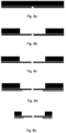
- the exemplary active charged particle optics component 3000 may be fabricated by employing a sequence of suitable techniques. This is depicted in Fig. 4 .
- a suitable fabrication technique may comprise etching away a block of bulk silicon so as to produce a groove in the bulk silicon.
- the etching technique may comprise, for example, a deep reactive ion-etching technique.
- a width of the groove may be chosen to correspond to the desired separation, such as 10 ⁇ m or even smaller, between the electrodes 302.
- An advantage of using etching may be that the process may be precisely controlled.
- the depth of the groove may be controlled by controlling the etching time and/or the etching rate (that may be known based on the etchant used).
- the width of the groove may be controlled by choosing the etchant appropriately. If a crystalline material is used for the electrodes 302, for example, the etchant may be chosen such that the rate of etching depends on the crystal face that is exposed. A suitable choice of etchant may be such that the rate of etching is fastest in the vertical direction. A further advantage of employing an etching process may be that a surface roughness of the fabricated microstructures may be significantly low. For example, a maximum surface roughness of Ra 0.05 ⁇ m may be obtained. Thus, the cavity or the surfaces between the electrodes 302 may be precisely shaped. This step is depicted in Fig. 4a , where grooves along the line 3020 are etched into bulk silicon 3000.
- the bulk silicon 3000 may not be etched right through so as to produce disjoint silicon electrodes 302 yet, so as to not adversely affect the spacing between the electrodes 302 that are fabricated. Rather, in a further step, depicted in Fig. 4b , the bulk silicon 3000 with the grooves may be glued on to a substrate/membrane 3060 such as glass, Pyrex, or a silicon wafer covered with an insulator (such as silica). This may help provide stability to the bulk silicon 3000 without affecting the width of the grooves 3020 (and thus the separation between the electrodes 302). The width of the separation between etched Si electrodes is getting larger when moving away from a center of active elements.
- a substrate/membrane 3060 such as glass, Pyrex, or a silicon wafer covered with an insulator (such as silica).
- the electrodes are floating in vacuum and a breakdown voltage threshold is 10KV/mm, so the distances could be kept smaller but at the outside, when electrodes are resting on an insulator, the breakdown threshold is governed by the surface creepage distance on the insulator (which is effectively, the distance between the electrodes). Thus, it can be advantageous to make this distance larger and to not necessarily form straight lines. Any other shape can be used as well. These separations could be uses for gluing the electrodes to the insulator.
- the electrodes 302 may be separated by dicing along the grooves 3020, as depicted in Fig. 4c . Any trailing edges of the bulk silicon 3000 may also be diced away.
- the final charged particle optics component 300 is depicted in Fig. 4d . Dicing may be accomplished by means of a laser, or any other suitable means of dicing.
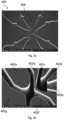
- Fig. 5 depicts an image of an exemplary charged particle optics component 400 fabricated in a lab.
- Fig. 5a depicts a zoomed-out view of the component 400
- Fig. 5b depicts a zoomed-in view.
- the charged particle optics component 400 comprises 7 electrodes 402 (a through g).
- the 7 electrodes 402 may be used to generate two adjacent quadrupole electrostatic fields, for example. In this case the two sets of quadrupoles share one electrode, as can be seen.
- the component 400 comprises alignment markers 408 that may be used for aligning the charged particle optics component 400 in the microscopy system 100. These alignment markers 408 may be patterned on the electrodes 402 or on an underlying substrate 406 (not shown) thereof, using any suitable lithography technique.
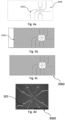
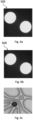
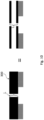
- Fig. 6a depicts an active charged particle optics component 500 fabricated as described above for use in a microscopy system 100 comprising an electron beam 107 with a beam energy of up to 60 KeV.
- Fig. 6b depicts another active charged particle optics component 600, comprising five times thicker electrodes, fabricated as described above for use in a microscopy system 100 comprising an electron beam 107 with a beam energy of up to 300 KeV. Comparing figures 6a and 6b , it may be appreciated that even though the thickness of the electrodes is increased by a factor of 5, the precision of the apertures (that may correspond to the separation, d, between the electrodes 202 in Fig. 2 ) is similar. Thus, the present invention may allow fabrication of active charged particle optics components for use with beams 107 of energies significantly larger than 10 KeV.
- Fig. 6c shows how electrodes can circumscribe a circular structure with respect to the embodiment shown in Fig. 5 .
- This can be formed by a cross-section of a hypothetical cylinder, as a circle, in order to define a free space for a beam to pass the electrodes. In this manner two pathways, each for one charged particle beam, can be formed very efficiently.
- Fig. 7 exemplifies a preferred device and its principal way of fabrication according to the present invention.
- an electrode component or electrode assembly 302 can be arranged at the bottom for fabrication purposes. In the example shown, it is a quadrupole assembly.
- an aperture plate or substrate 306 On top is an aperture plate or substrate 306 that has a larger aperture than is shown in Fig. 3 . This is advantageous as the charged particles beam not to influenced by the substrate.
- a BLA beam limiting aperture
- This can be arranged on top of element 300. This can be realized in order to prevent direct interaction of the charged particle beam with the electrodes.
- Fig. 8a shows in more detail an aperture plate or supporting structure and its preferred first step of fabrication.
- a wafer structure or any other material is treated to form the apertures that are aligned with electrodes in the later-described electrode component.
- the electrodes are formed by a lithography and then an etching step.
- the lithography can be a high-resolution lithography step, such as an EBPG lithography step.
- the etching can be done by a highly anisotropic (dry) deep reactive ion etching (DRIE) process.
- DRIE deep reactive ion etching
- the aperture is formed by another lithography step, such as by NUV lithography, followed by another etching, such as the DRIE etching, mentioned before.
- the intermediate material is further removed, as shown in Fig. 8c .
- the techniques for that can be a stripping of the insulating Si oxide and a metallization of the remaining structure.
- an insulator that can comprise or consist of glass can be attached and then the final structure can be obtained by dicing and cleaning according to Fig. 8e .
- Electrical connections such as the ones to electrodes 302a and 302b, can be formed by accommodating electrical connections in the layer 304.
- Figs. 9a-9e The electrode component or assembly and a possible fabrication is further exemplified by Figs. 9a-9e .
- oxide can be formed on bare Si by a PECVD process. This is an example only.
- a lithographic step such as an EBPG step and a DRIE step, can be chosen to form the electrode structure, such as a quadrupole, with optional alignment patterns.
- a lithographic step such as a NUV lithography
- considerable material can be removed, followed by a DRIE etching or other etching steps.
- the Si oxide can be removed by another etching, followed by a metallization, see Fig. 9c .
- a spacer can be added.
- Fig. 9e exemplifies the dicing and further cleaning of the electrode component or quadrupole assembly.
- the electrodes form a thickness L with different arrangements of spacers or insulators, depending on the needs.
- the thickness L establishes the effective thickness.
- Fig. 13 is exemplifying a known corrector concept based on four quadrupoles (e.g., four multipoles, also known as a " Russian Quadruplet").
- a known corrector concept based on four quadrupoles (e.g., four multipoles, also known as a " Russian Quadruplet").
- an alignment of at least 1 ⁇ m accuracy between the individual elements is advantageous (between Q1, Q ,.).
- the fabrication accuracy isn't only needed to make individual electrodes but also needed to align the stack with the assistance of alignment marker between different elements (different Q in above example).
- At least one step of the fabrication method for the electrode component (300) may be chosen based on a desired maximum absolute dimensional tolerance.
- the desired maximum absolute dimensional tolerance may be based on characteristics of a charged particle system comprising the device as described above. For example, it may be based on the beam energy of the beam as described above.
- the desired maximum absolute dimensional tolerance may be based on a maximum voltage to be applied to any of the at least two electrodes (302a, b).
- the desired maximum absolute dimensional tolerance may be based on the effective length of any of the at least two electrodes (302a, b).
- the desired maximum absolute dimensional tolerance may be based on an aberration coefficient of a lens of the charged particle system.
- the desired maximum absolute dimensional tolerance may be determined, and based thereon, at least one step of the fabrication method may be chosen.
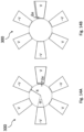
- an electrostatic multipole element with a radius of R and effective length L that produces a hexapole field (disregarding the fringe field), see Figs. 14 (a, b) and Fig. 15 .
- the hexapole potential can be written as: ⁇ 3 x y ⁇ V R 3 x 3 ⁇ 3 xy 2
- ⁇ parasitic ⁇ m 1 R m Re V m x + iy m , with V m ⁇ ⁇ V ⁇ s R .
- Each (complex) Fourier component V m may lead to parasitic primary aberrations and combination aberrations.
- the primary parasitic aberration is m-fold astigmatism with an aberration coefficient of A m -1 .
- the error ⁇ s in fabricating elements may lead to a change in the probe diameter d50, and the change may depend on characteristics such as the effective length L of the electrodes 302 (a, b), the beam energy U, or the spherical aberration coefficient of another component.
- the desired maximum absolute dimensional tolerance may be determined by, for example, requiring that the probe diameter d50 does not exceed a certain threshold. For example, if the probe diameter d50 in the absence of any geometric or chromatic aberrations would be 1.25 ⁇ , one may require that the probe diameter d50 in the presence of geometric or chromatic aberrations is no greater than 2 ⁇ . This may impose an upper limit on the size of
- the desired maximum absolute dimensional tolerance may be determined based on a desired maximum variation in the effect (such as variation in the probe diameter d50 described above) of the electrode component when used e.g., in a charged particle system.
- a desired maximum variation in the effect such as variation in the probe diameter d50 described above
- other methods such as, for example, an artificial-intelligence based method, may be employed to corroborate the desired maximum absolute dimensional tolerance with the desired maximum variation in the effect of the electrode component.
- embodiments of the present invention aim to thus provide an active charged particle optics component for use with high-energy beams that may be fabricated robustly, precisely, and efficiently using the processes described above. Embodiments of the present invention may thus provide an effective avenue to improving the resolution of microscopy systems.
- step (X) preceding step (Z) encompasses the situation that step (X) is performed directly before step (Z), but also the situation that (X) is performed before one or more steps (Y1), ..., followed by step (Z).
- step (Z) encompasses the situation that step (X) is performed directly before step (Z), but also the situation that (X) is performed before one or more steps (Y1), ..., followed by step (Z).
Landscapes
- Chemical & Material Sciences (AREA)
- Analytical Chemistry (AREA)
- Physics & Mathematics (AREA)
- General Physics & Mathematics (AREA)
- Engineering & Computer Science (AREA)
- Manufacturing & Machinery (AREA)
- Electron Beam Exposure (AREA)
- Exposure And Positioning Against Photoresist Photosensitive Materials (AREA)
Applications Claiming Priority (1)
| Application Number | Priority Date | Filing Date | Title |
|---|---|---|---|
| US17/883,495 US12525422B2 (en) | 2022-08-08 | 2022-08-08 | Charged particle optics components and their fabrication |
Publications (2)
| Publication Number | Publication Date |
|---|---|
| EP4322196A2 true EP4322196A2 (de) | 2024-02-14 |
| EP4322196A3 EP4322196A3 (de) | 2025-06-25 |
Family
ID=87567533
Family Applications (1)
| Application Number | Title | Priority Date | Filing Date |
|---|---|---|---|
| EP23190282.6A Pending EP4322196A3 (de) | 2022-08-08 | 2023-08-08 | Optische komponenten für geladene teilchen und ihre herstellung |
Country Status (5)
| Country | Link |
|---|---|
| US (1) | US12525422B2 (de) |
| EP (1) | EP4322196A3 (de) |
| JP (1) | JP2024023162A (de) |
| KR (1) | KR20240020662A (de) |
| CN (1) | CN117542714A (de) |
Families Citing this family (1)
| Publication number | Priority date | Publication date | Assignee | Title |
|---|---|---|---|---|
| US12525422B2 (en) * | 2022-08-08 | 2026-01-13 | Fei Company | Charged particle optics components and their fabrication |
Family Cites Families (26)
| Publication number | Priority date | Publication date | Assignee | Title |
|---|---|---|---|---|
| JPS6321736A (ja) | 1986-07-15 | 1988-01-29 | Matsushita Electric Ind Co Ltd | 荷電粒子ビ−ム偏向板の製造法 |
| JP2641437B2 (ja) * | 1987-02-27 | 1997-08-13 | 株式会社日立製作所 | 荷電粒子線装置 |
| JPH08115800A (ja) | 1994-10-19 | 1996-05-07 | Kyocera Corp | 加速管 |
| JPH10214779A (ja) * | 1997-01-31 | 1998-08-11 | Canon Inc | 電子ビーム露光方法及び該方法を用いたデバイス製造方法 |
| JP4217933B2 (ja) | 1999-06-18 | 2009-02-04 | ソニー株式会社 | 電子放出源及びその製造方法、並びにその電子放出源を用いたディスプレイ装置 |
| JP3763446B2 (ja) * | 1999-10-18 | 2006-04-05 | キヤノン株式会社 | 静電レンズ、電子ビーム描画装置、荷電ビーム応用装置、および、デバイス製造方法 |
| AU1926501A (en) * | 1999-11-23 | 2001-06-04 | Ion Diagnostics, Inc. | Electron optics for multi-beam electron beam lithography tool |
| DE60011031T2 (de) * | 2000-02-01 | 2005-06-23 | ICT Integrated Circuit Testing Gesellschaft für Halbleiterprüftechnik mbH | Optische Säule für Teilchenstrahlvorrichtung |
| US6943351B2 (en) * | 2000-02-19 | 2005-09-13 | Multibeam Systems, Inc. | Multi-column charged particle optics assembly |
| JP4585661B2 (ja) | 2000-03-31 | 2010-11-24 | キヤノン株式会社 | 電子光学系アレイ、荷電粒子線露光装置およびデバイス製造方法 |
| JP4947842B2 (ja) * | 2000-03-31 | 2012-06-06 | キヤノン株式会社 | 荷電粒子線露光装置 |
| US6630677B1 (en) | 2001-08-29 | 2003-10-07 | Advanced Micro Devices, Inc. | Electrostatic lens having glassy graphite electrodes |
| JP4115410B2 (ja) | 2004-03-12 | 2008-07-09 | キヤノン株式会社 | 電子放出素子、電子源ならびに画像表示装置の製造方法および電子放出素子の駆動方法 |
| EP1851784B8 (de) * | 2005-02-11 | 2016-10-19 | IMS Nanofabrication AG | Vorrichtung zur belichtung mit geladenen teilchen mit elektrostatischer zonenplatte |
| JP4881661B2 (ja) * | 2006-06-20 | 2012-02-22 | 株式会社日立ハイテクノロジーズ | 荷電粒子線装置 |
| EP2378537B1 (de) * | 2010-04-19 | 2014-02-12 | ICT Integrated Circuit Testing Gesellschaft für Halbleiterprüftechnik mbH | Verfahren zum Betreiben einer Teilchenstrahlvorrichtung |
| US8319192B2 (en) * | 2010-08-24 | 2012-11-27 | Hermes Microvision Inc. | Charged particle apparatus |
| JP5860642B2 (ja) * | 2011-09-07 | 2016-02-16 | 株式会社日立ハイテクノロジーズ | 走査電子顕微鏡 |
| JP2013165200A (ja) | 2012-02-13 | 2013-08-22 | Canon Inc | 荷電粒子線レンズ |
| JP2014041947A (ja) | 2012-08-23 | 2014-03-06 | Canon Inc | 荷電粒子線レンズ |
| JP6320186B2 (ja) * | 2014-06-16 | 2018-05-09 | 株式会社日立ハイテクノロジーズ | 荷電粒子線応用装置 |
| US10249472B2 (en) * | 2017-07-13 | 2019-04-02 | ICT Integrated Circuit Testing Gesellschaft für Halbleiterprüftechnik mbH | Charged particle beam device, charged particle beam influencing device, and method of operating a charged particle beam device |
| US10784070B2 (en) * | 2018-10-19 | 2020-09-22 | ICT Integrated Circuit Testing Gesellschaft für Halbleiterprüftechnik mbH | Charged particle beam device, field curvature corrector, and methods of operating a charged particle beam device |
| EP4009349A1 (de) | 2020-12-03 | 2022-06-08 | ASML Netherlands B.V. | Vorrrichtung für geladene teilchen, kalibrierverfahren, prüfverfahren |
| WO2022258271A1 (en) * | 2021-06-08 | 2022-12-15 | Asml Netherlands B.V. | Charged particle apparatus and method |
| US12525422B2 (en) * | 2022-08-08 | 2026-01-13 | Fei Company | Charged particle optics components and their fabrication |
-
2022
- 2022-08-08 US US17/883,495 patent/US12525422B2/en active Active
-
2023
- 2023-07-19 KR KR1020230093677A patent/KR20240020662A/ko active Pending
- 2023-08-07 JP JP2023128816A patent/JP2024023162A/ja active Pending
- 2023-08-08 CN CN202310990794.XA patent/CN117542714A/zh active Pending
- 2023-08-08 EP EP23190282.6A patent/EP4322196A3/de active Pending
Also Published As
| Publication number | Publication date |
|---|---|
| JP2024023162A (ja) | 2024-02-21 |
| KR20240020662A (ko) | 2024-02-15 |
| CN117542714A (zh) | 2024-02-09 |
| EP4322196A3 (de) | 2025-06-25 |
| US12525422B2 (en) | 2026-01-13 |
| US20240047171A1 (en) | 2024-02-08 |
Similar Documents
| Publication | Publication Date | Title |
|---|---|---|
| KR102903956B1 (ko) | 멀티빔 생성 유닛 및 멀티빔 편향 유닛의 명백한 개선 | |
| USRE46452E1 (en) | Electrostatic lens structure | |
| EP2556527B1 (de) | System zur erkennung von geladenen partikeln und inspektionssystem mit mehreren teilstrahlen | |
| KR20130129109A (ko) | 정전렌즈의 전극 및 그 제조 방법 | |
| US20240170252A1 (en) | Multi-beam generating unit with increased focusing power | |
| CN1663013A (zh) | 粒子束发生器 | |
| TW201729233A (zh) | 靜電多極元件、靜電多極裝置及製造靜電多極元件的方法 | |
| US20120319001A1 (en) | Charged particle beam lens | |
| JP7410311B2 (ja) | 静電レンズ設計 | |
| WO2001009922A1 (en) | Electrostatic alignment of a charged particle beam | |
| US12525422B2 (en) | Charged particle optics components and their fabrication | |
| JP2007266525A (ja) | 荷電粒子線レンズアレイ、該荷電粒子線レンズアレイを用いた荷電粒子線露光装置 | |
| TWI923572B (zh) | 多射束光柵單元與多射束帶電粒子顯微鏡 | |
| US20240355575A1 (en) | Beam manipulator in charged particle-beam apparatus | |
| JP4402077B2 (ja) | 荷電粒子線レンズアレイ、露光装置及びデバイス製造方法 | |
| JP2025521419A (ja) | 電子光学アセンブリ用の絶縁スペーサ | |
| CN120898265A (zh) | 电子光学板 | |
| JP2025532037A (ja) | 電子光学要素のアライメント |
Legal Events
| Date | Code | Title | Description |
|---|---|---|---|
| PUAI | Public reference made under article 153(3) epc to a published international application that has entered the european phase |
Free format text: ORIGINAL CODE: 0009012 |
|
| STAA | Information on the status of an ep patent application or granted ep patent |
Free format text: STATUS: THE APPLICATION HAS BEEN PUBLISHED |
|
| AK | Designated contracting states |
Kind code of ref document: A2 Designated state(s): AL AT BE BG CH CY CZ DE DK EE ES FI FR GB GR HR HU IE IS IT LI LT LU LV MC ME MK MT NL NO PL PT RO RS SE SI SK SM TR |
|
| RIC1 | Information provided on ipc code assigned before grant |
Ipc: H01J 37/28 20060101ALI20240725BHEP Ipc: H01J 9/14 20060101ALI20240725BHEP Ipc: H01J 1/46 20060101ALI20240725BHEP Ipc: H01J 37/153 20060101ALI20240725BHEP Ipc: H01J 37/147 20060101AFI20240725BHEP |
|
| PUAL | Search report despatched |
Free format text: ORIGINAL CODE: 0009013 |
|
| AK | Designated contracting states |
Kind code of ref document: A3 Designated state(s): AL AT BE BG CH CY CZ DE DK EE ES FI FR GB GR HR HU IE IS IT LI LT LU LV MC ME MK MT NL NO PL PT RO RS SE SI SK SM TR |
|
| RIC1 | Information provided on ipc code assigned before grant |
Ipc: H01J 37/28 20060101ALI20250516BHEP Ipc: H01J 9/14 20060101ALI20250516BHEP Ipc: H01J 1/46 20060101ALI20250516BHEP Ipc: H01J 37/153 20060101ALI20250516BHEP Ipc: H01J 37/147 20060101AFI20250516BHEP |
|
| STAA | Information on the status of an ep patent application or granted ep patent |
Free format text: STATUS: REQUEST FOR EXAMINATION WAS MADE |
|
| 17P | Request for examination filed |
Effective date: 20251231 |