EP4310921A1 - Thin film transistor and method for producing thin film transistor - Google Patents
Thin film transistor and method for producing thin film transistor Download PDFInfo
- Publication number
- EP4310921A1 EP4310921A1 EP22771429.2A EP22771429A EP4310921A1 EP 4310921 A1 EP4310921 A1 EP 4310921A1 EP 22771429 A EP22771429 A EP 22771429A EP 4310921 A1 EP4310921 A1 EP 4310921A1
- Authority
- EP
- European Patent Office
- Prior art keywords
- gate insulating
- insulating coating
- layer
- thickness
- thin film
- Prior art date
- Legal status (The legal status is an assumption and is not a legal conclusion. Google has not performed a legal analysis and makes no representation as to the accuracy of the status listed.)
- Granted
Links
Images



Classifications
-
- H—ELECTRICITY
- H10—SEMICONDUCTOR DEVICES; ELECTRIC SOLID-STATE DEVICES NOT OTHERWISE PROVIDED FOR
- H10D—INORGANIC ELECTRIC SEMICONDUCTOR DEVICES
- H10D30/00—Field-effect transistors [FET]
- H10D30/01—Manufacture or treatment
- H10D30/021—Manufacture or treatment of FETs having insulated gates [IGFET]
- H10D30/031—Manufacture or treatment of FETs having insulated gates [IGFET] of thin-film transistors [TFT]
-
- H—ELECTRICITY
- H10—SEMICONDUCTOR DEVICES; ELECTRIC SOLID-STATE DEVICES NOT OTHERWISE PROVIDED FOR
- H10D—INORGANIC ELECTRIC SEMICONDUCTOR DEVICES
- H10D30/00—Field-effect transistors [FET]
- H10D30/60—Insulated-gate field-effect transistors [IGFET]
- H10D30/67—Thin-film transistors [TFT]
- H10D30/6729—Thin-film transistors [TFT] characterised by the electrodes
-
- H—ELECTRICITY
- H10—SEMICONDUCTOR DEVICES; ELECTRIC SOLID-STATE DEVICES NOT OTHERWISE PROVIDED FOR
- H10D—INORGANIC ELECTRIC SEMICONDUCTOR DEVICES
- H10D30/00—Field-effect transistors [FET]
- H10D30/60—Insulated-gate field-effect transistors [IGFET]
- H10D30/67—Thin-film transistors [TFT]
- H10D30/6729—Thin-film transistors [TFT] characterised by the electrodes
- H10D30/673—Thin-film transistors [TFT] characterised by the electrodes characterised by the shapes, relative sizes or dispositions of the gate electrodes
-
- H—ELECTRICITY
- H10—SEMICONDUCTOR DEVICES; ELECTRIC SOLID-STATE DEVICES NOT OTHERWISE PROVIDED FOR
- H10D—INORGANIC ELECTRIC SEMICONDUCTOR DEVICES
- H10D30/00—Field-effect transistors [FET]
- H10D30/60—Insulated-gate field-effect transistors [IGFET]
- H10D30/67—Thin-film transistors [TFT]
- H10D30/6729—Thin-film transistors [TFT] characterised by the electrodes
- H10D30/6737—Thin-film transistors [TFT] characterised by the electrodes characterised by the electrode materials
- H10D30/6739—Conductor-insulator-semiconductor electrodes
-
- H—ELECTRICITY
- H10—SEMICONDUCTOR DEVICES; ELECTRIC SOLID-STATE DEVICES NOT OTHERWISE PROVIDED FOR
- H10D—INORGANIC ELECTRIC SEMICONDUCTOR DEVICES
- H10D30/00—Field-effect transistors [FET]
- H10D30/60—Insulated-gate field-effect transistors [IGFET]
- H10D30/67—Thin-film transistors [TFT]
- H10D30/6758—Thin-film transistors [TFT] characterised by the insulating substrates
-
- H—ELECTRICITY
- H10—SEMICONDUCTOR DEVICES; ELECTRIC SOLID-STATE DEVICES NOT OTHERWISE PROVIDED FOR
- H10D—INORGANIC ELECTRIC SEMICONDUCTOR DEVICES
- H10D30/00—Field-effect transistors [FET]
- H10D30/60—Insulated-gate field-effect transistors [IGFET]
- H10D30/67—Thin-film transistors [TFT]
- H10D30/674—Thin-film transistors [TFT] characterised by the active materials
- H10D30/6755—Oxide semiconductors, e.g. zinc oxide, copper aluminium oxide or cadmium stannate
-
- H—ELECTRICITY
- H10—SEMICONDUCTOR DEVICES; ELECTRIC SOLID-STATE DEVICES NOT OTHERWISE PROVIDED FOR
- H10P—GENERIC PROCESSES OR APPARATUS FOR THE MANUFACTURE OR TREATMENT OF DEVICES COVERED BY CLASS H10
- H10P14/00—Formation of materials, e.g. in the shape of layers or pillars
- H10P14/60—Formation of materials, e.g. in the shape of layers or pillars of insulating materials
- H10P14/63—Formation of materials, e.g. in the shape of layers or pillars of insulating materials characterised by the formation processes
- H10P14/6326—Deposition processes
- H10P14/6328—Deposition from the gas or vapour phase
- H10P14/6334—Deposition from the gas or vapour phase using decomposition or reaction of gaseous or vapour phase compounds, i.e. chemical vapour deposition
- H10P14/6336—Deposition from the gas or vapour phase using decomposition or reaction of gaseous or vapour phase compounds, i.e. chemical vapour deposition in the presence of a plasma [PECVD]
-
- H—ELECTRICITY
- H10—SEMICONDUCTOR DEVICES; ELECTRIC SOLID-STATE DEVICES NOT OTHERWISE PROVIDED FOR
- H10P—GENERIC PROCESSES OR APPARATUS FOR THE MANUFACTURE OR TREATMENT OF DEVICES COVERED BY CLASS H10
- H10P14/00—Formation of materials, e.g. in the shape of layers or pillars
- H10P14/60—Formation of materials, e.g. in the shape of layers or pillars of insulating materials
- H10P14/63—Formation of materials, e.g. in the shape of layers or pillars of insulating materials characterised by the formation processes
- H10P14/6326—Deposition processes
- H10P14/6328—Deposition from the gas or vapour phase
- H10P14/6334—Deposition from the gas or vapour phase using decomposition or reaction of gaseous or vapour phase compounds, i.e. chemical vapour deposition
- H10P14/6339—Deposition from the gas or vapour phase using decomposition or reaction of gaseous or vapour phase compounds, i.e. chemical vapour deposition deposition by cyclic CVD, e.g. ALD, ALE or pulsed CVD
-
- H—ELECTRICITY
- H10—SEMICONDUCTOR DEVICES; ELECTRIC SOLID-STATE DEVICES NOT OTHERWISE PROVIDED FOR
- H10P—GENERIC PROCESSES OR APPARATUS FOR THE MANUFACTURE OR TREATMENT OF DEVICES COVERED BY CLASS H10
- H10P14/00—Formation of materials, e.g. in the shape of layers or pillars
- H10P14/60—Formation of materials, e.g. in the shape of layers or pillars of insulating materials
- H10P14/63—Formation of materials, e.g. in the shape of layers or pillars of insulating materials characterised by the formation processes
- H10P14/6326—Deposition processes
- H10P14/6342—Liquid deposition, e.g. spin-coating, sol-gel techniques or spray coating
-
- H—ELECTRICITY
- H10—SEMICONDUCTOR DEVICES; ELECTRIC SOLID-STATE DEVICES NOT OTHERWISE PROVIDED FOR
- H10P—GENERIC PROCESSES OR APPARATUS FOR THE MANUFACTURE OR TREATMENT OF DEVICES COVERED BY CLASS H10
- H10P14/00—Formation of materials, e.g. in the shape of layers or pillars
- H10P14/60—Formation of materials, e.g. in the shape of layers or pillars of insulating materials
- H10P14/66—Formation of materials, e.g. in the shape of layers or pillars of insulating materials characterised by the type of materials
- H10P14/668—Formation of materials, e.g. in the shape of layers or pillars of insulating materials characterised by the type of materials the materials being characterised by the deposition precursor materials
- H10P14/6681—Formation of materials, e.g. in the shape of layers or pillars of insulating materials characterised by the type of materials the materials being characterised by the deposition precursor materials the precursor containing a compound comprising Si
- H10P14/6682—Formation of materials, e.g. in the shape of layers or pillars of insulating materials characterised by the type of materials the materials being characterised by the deposition precursor materials the precursor containing a compound comprising Si the compound being a silane, e.g. disilane, methylsilane or chlorosilane
-
- H—ELECTRICITY
- H10—SEMICONDUCTOR DEVICES; ELECTRIC SOLID-STATE DEVICES NOT OTHERWISE PROVIDED FOR
- H10P—GENERIC PROCESSES OR APPARATUS FOR THE MANUFACTURE OR TREATMENT OF DEVICES COVERED BY CLASS H10
- H10P14/00—Formation of materials, e.g. in the shape of layers or pillars
- H10P14/60—Formation of materials, e.g. in the shape of layers or pillars of insulating materials
- H10P14/68—Organic materials, e.g. photoresists
- H10P14/683—Organic materials, e.g. photoresists carbon-based polymeric organic materials, e.g. polyimides, poly cyclobutene or PVC
-
- H—ELECTRICITY
- H10—SEMICONDUCTOR DEVICES; ELECTRIC SOLID-STATE DEVICES NOT OTHERWISE PROVIDED FOR
- H10P—GENERIC PROCESSES OR APPARATUS FOR THE MANUFACTURE OR TREATMENT OF DEVICES COVERED BY CLASS H10
- H10P14/00—Formation of materials, e.g. in the shape of layers or pillars
- H10P14/60—Formation of materials, e.g. in the shape of layers or pillars of insulating materials
- H10P14/69—Inorganic materials
- H10P14/692—Inorganic materials composed of oxides, glassy oxides or oxide-based glasses
- H10P14/6921—Inorganic materials composed of oxides, glassy oxides or oxide-based glasses containing silicon
- H10P14/69215—Inorganic materials composed of oxides, glassy oxides or oxide-based glasses containing silicon the material being a silicon oxide, e.g. SiO2
-
- H—ELECTRICITY
- H10—SEMICONDUCTOR DEVICES; ELECTRIC SOLID-STATE DEVICES NOT OTHERWISE PROVIDED FOR
- H10P—GENERIC PROCESSES OR APPARATUS FOR THE MANUFACTURE OR TREATMENT OF DEVICES COVERED BY CLASS H10
- H10P14/00—Formation of materials, e.g. in the shape of layers or pillars
- H10P14/60—Formation of materials, e.g. in the shape of layers or pillars of insulating materials
- H10P14/69—Inorganic materials
- H10P14/692—Inorganic materials composed of oxides, glassy oxides or oxide-based glasses
- H10P14/6921—Inorganic materials composed of oxides, glassy oxides or oxide-based glasses containing silicon
- H10P14/6922—Inorganic materials composed of oxides, glassy oxides or oxide-based glasses containing silicon the material containing Si, O and at least one of H, N, C, F or other non-metal elements, e.g. SiOC, SiOC:H or SiONC
- H10P14/6927—Inorganic materials composed of oxides, glassy oxides or oxide-based glasses containing silicon the material containing Si, O and at least one of H, N, C, F or other non-metal elements, e.g. SiOC, SiOC:H or SiONC the material being a silicon oxynitride, e.g. SiON or SiON:H
-
- H—ELECTRICITY
- H10—SEMICONDUCTOR DEVICES; ELECTRIC SOLID-STATE DEVICES NOT OTHERWISE PROVIDED FOR
- H10P—GENERIC PROCESSES OR APPARATUS FOR THE MANUFACTURE OR TREATMENT OF DEVICES COVERED BY CLASS H10
- H10P14/00—Formation of materials, e.g. in the shape of layers or pillars
- H10P14/60—Formation of materials, e.g. in the shape of layers or pillars of insulating materials
- H10P14/69—Inorganic materials
- H10P14/692—Inorganic materials composed of oxides, glassy oxides or oxide-based glasses
- H10P14/6938—Inorganic materials composed of oxides, glassy oxides or oxide-based glasses the material containing at least one metal element, e.g. metal oxides, metal oxynitrides or metal oxycarbides
- H10P14/6939—Inorganic materials composed of oxides, glassy oxides or oxide-based glasses the material containing at least one metal element, e.g. metal oxides, metal oxynitrides or metal oxycarbides characterised by the metal
- H10P14/69391—Inorganic materials composed of oxides, glassy oxides or oxide-based glasses the material containing at least one metal element, e.g. metal oxides, metal oxynitrides or metal oxycarbides characterised by the metal the material containing aluminium, e.g. Al2O3
-
- H—ELECTRICITY
- H10—SEMICONDUCTOR DEVICES; ELECTRIC SOLID-STATE DEVICES NOT OTHERWISE PROVIDED FOR
- H10P—GENERIC PROCESSES OR APPARATUS FOR THE MANUFACTURE OR TREATMENT OF DEVICES COVERED BY CLASS H10
- H10P14/00—Formation of materials, e.g. in the shape of layers or pillars
- H10P14/60—Formation of materials, e.g. in the shape of layers or pillars of insulating materials
- H10P14/69—Inorganic materials
- H10P14/694—Inorganic materials composed of nitrides
- H10P14/6943—Inorganic materials composed of nitrides containing silicon
- H10P14/69433—Inorganic materials composed of nitrides containing silicon the material being a silicon nitride not containing oxygen, e.g. SixNy or SixByNz
Definitions
- the present disclosure relates to a thin film transistor including, as a gate insulating layer, a laminate of a first gate insulating coating made of an organic polymer compound or an organic-inorganic composite material and a second gate insulating coating made of an inorganic silicon compound, and a method for manufacturing the thin film transistor.
- a thin film transistor having a gate insulating layer including an organic polymer compound film and an inorganic silicon compound film combines a good withstand voltage and flexibility.
- the relative permittivity ⁇ A used to calculate the dielectric property value is the relative permittivity of the first gate insulating coating containing the organic polymer compound.
- the thickness d A is the thickness of the first gate insulating coating.
- the relative permittivity ⁇ B used to calculate the dielectric property value is the relative permittivity of the second gate insulating coating containing the inorganic polymer compound.
- the thickness d B is the thickness of the second gate insulating coating.
- the relative permittivity of the gate insulating layer is an index value indicating whether a certain amount of charge induced per unit area can be secured. It is also an index value indicating whether current leakage between the gate electrode and another electrode can be suppressed. Meanwhile, the relative permittivity of the gate insulating layer is not closely related to the electrical durability against bending of the flexible substrate. Similarly, the above-described dielectric property value, which compares the susceptibility to dielectric polarization of the first gate insulating coating to that of the second gate insulating coating, is also not closely related to the electrical durability against bending of the flexible substrate. As a result, when the configuration has a relative permittivity within a predetermined range, or even when the configuration has a dielectric property value within the predetermined range, it may not be possible to increase the electrical durability against bending of the flexible substrate.
- An aspect of a thin film transistor includes a flexible substrate having a support surface; a gate electrode layer located in a first part of the support surface; a gate insulating layer covering a second part of the support surface and the gate electrode layer; a semiconductor layer sandwiching the gate insulating layer with the gate electrode layer; a source electrode layer in contact with a first end of the semiconductor layer with no insulating layer between the source electrode layer and the semiconductor layer; and a drain electrode layer in contact with a second end of the semiconductor layer with no insulating layer between the drain electrode layer and the semiconductor layer.
- the gate insulating layer includes a first gate insulating coating made of an organic polymer compound or an organic-inorganic composite material and covering the second part and the gate electrode layer, and a second gate insulating coating made of one selected from the group consisting of silicon oxide, silicon nitride, silicon oxynitride, and aluminum oxide.
- the second gate insulating coating is sandwiched between the first gate insulating coating and a semiconductor layer.
- the first gate insulating coating has a thickness of 100 nm or greater and 1500 nm or less, and a product of the thickness and Young's modulus of the first gate insulating coating is 300 nm ⁇ GPa or greater and 30000 nm ⁇ GPa or less.
- the second gate insulating coating has a thickness of 2 nm or greater and 30 nm or less, and a product of the thickness and Young's modulus of the second gate insulating coating is 100 nm ⁇ GPa or greater and 9000 nm ⁇ GPa or less.
- An aspect of a method of manufacturing a thin film transistor includes forming a gate electrode layer on a first part of a support surface of a flexible substrate; forming a gate insulating layer covering a second part of the support surface and the gate electrode layer; forming a semiconductor layer sandwiching the gate insulating layer with the gate electrode layer; and forming a source electrode layer in contact with a first end of the semiconductor layer with no insulating layer between the source electrode layer and the semiconductor layer, and a drain electrode layer in contact with a second end of the semiconductor layer with no insulating layer between the drain electrode layer and the semiconductor layer.
- Forming the gate insulating layer includes forming, by a coating method, a first gate insulating coating made of an organic polymer compound or an organic-inorganic composite material and covering the second part and the gate electrode layer, and forming a second gate insulating coating made of one selected from the group consisting of silicon oxide, silicon nitride, silicon oxynitride, and aluminum oxide, and sandwiched between the first gate insulating coating and the semiconductor layer.
- the first gate insulating coating has a thickness of 100 nm or greater and 1500 nm or less, and a product of the thickness and Young's modulus of the first gate insulating coating is 300 nm ⁇ GPa or greater and 30000 nm ⁇ GPa or less.
- the second gate insulating coating has a thickness of 2 nm or greater and 30 nm or less, and a product of the thickness and Young's modulus of the second gate insulating coating is 100 nm GPa or greater and 9000 nm GPa or less.
- An as aspect of a thin film transistor includes a flexible substrate having a support surface; a gate electrode layer located in a first part of the support surface; a gate insulating layer covering a second part of the support surface and the gate electrode layer; a semiconductor layer sandwiching the gate insulating layer with the gate electrode layer; a protective layer covering the semiconductor layer so that first and second regions on an upper surface of the semiconductor layer are exposed through the protective layer; a source electrode layer in contact with the first region; and a drain electrode layer in contact with the second region.
- the protective layer is made of an organic polymer compound or an organic-inorganic composite material.
- the gate insulating layer includes a first gate insulating coating made of an organic polymer compound or an organic-inorganic composite material and covering the second part and the gate electrode layer, and a second gate insulating coating made of one selected from the group consisting of silicon oxide, silicon nitride, silicon oxynitride, and aluminum oxide.
- the second gate insulating coating is sandwiched between the first gate insulating coating and a semiconductor layer.
- the first gate insulating coating has a thickness of 100 nm or greater and 1500 nm or less, and a product of the thickness and Young's modulus of the first gate insulating coating is 300 nm ⁇ GPa or greater and 30000 nm ⁇ GPa or less.
- the second gate insulating coating has a thickness of 2 nm or greater and 30 nm or less, and a product of the thickness and Young's modulus of the second gate insulating coating is 100 nm GPa or greater and 9000 nm GPa or less.
- An aspect of a method of manufacturing a thin film transistor includes: forming a gate electrode layer on a first part of a support surface of a flexible substrate; forming a gate insulating layer covering a second part of the support surface and the gate electrode layer; forming a semiconductor layer sandwiching the gate insulating layer with the gate electrode layer; forming a protective layer so that first and second regions on an upper surface of the semiconductor layer are exposed through the protective layer, the protective layer being made of an organic polymer compound or an organic-inorganic composite material; and forming a source electrode layer in contact with the first region, and a drain electrode layer in contact with the second region.
- Forming the gate insulating layer includes forming, by a coating method, a first gate insulating coating made of an organic polymer compound or an organic-inorganic composite material and covering the second part and the gate electrode layer, and forming a second gate insulating coating made of one selected from the group consisting of silicon oxide, silicon nitride, silicon oxynitride, and aluminum oxide, and sandwiched between the first gate insulating coating and the semiconductor layer.
- the first gate insulating coating has a thickness of 100 nm or greater and 1500 nm or less, a product of the thickness and Young's modulus of the first gate insulating coating is 300 nm ⁇ GPa or greater and 30000 nm ⁇ GPa or less, the second gate insulating coating has a thickness of 2 nm or greater and 30 nm or less, and a product of the thickness and Young's modulus of the second gate insulating coating is 100 nm ⁇ GPa or greater and 9000 nm ⁇ GPa or less.
- An as aspect of a thin film transistor includes a flexible substrate having a support surface; a gate electrode layer located in a first part of the support surface; a gate insulating layer covering a second part of the support surface and the gate electrode layer; a semiconductor layer sandwiching the gate insulating layer with the gate electrode layer; a protective layer covering the semiconductor layer so that first and second regions on an upper surface of the semiconductor layer are exposed through the protective layer; a source electrode layer in contact with the first region; and a drain electrode layer in contact with the second region.
- the protective layer is made of silicon oxide, silicon nitride, or silicon oxynitride.
- the gate insulating layer includes a first gate insulating coating made of an organic polymer compound or an organic-inorganic composite material and covering the second part and the gate electrode layer, and a second gate insulating coating made of one selected from the group consisting of silicon oxide, silicon nitride, silicon oxynitride, and aluminum oxide.
- the second gate insulating coating is sandwiched between the first gate insulating coating and a semiconductor layer.
- the first gate insulating coating has a thickness of 100 nm or greater and 1500 nm or less, and a product of the thickness and Young's modulus of the first gate insulating coating is 300 nm ⁇ GPa or greater and 30000 nm GPa or less.
- the second gate insulating coating has a thickness of 2 nm or greater and 30 nm or less, and a product of the thickness and Young's modulus of the second gate insulating coating is 100 nm ⁇ GPa or greater and 9000 nm ⁇ GPa or less.
- the protective layer has a thickness of 40 nm or greater and 60 nm or less, and a product of the thickness and Young's modulus of the protective layer is 2000 nm ⁇ GPa or greater and 9000 nm ⁇ GPa or less.
- a first embodiment of a thin film transistor and a method of manufacturing a thin film transistor will be described below. First, the multilayer structure of the thin film transistor will be described, then the constituent materials and dimensions of each layer of the thin film transistor will be described, and finally the method of manufacturing the thin film transistor will be described.
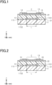
- Fig. 1 shows a first example of a multilayer structure of a thin film transistor
- Fig. 2 shows a second example of a multilayer structure of a thin film transistor.
- the upper and lower surfaces of each component of the thin film transistor will be described assuming it is oriented as in Figs. 1 and 2 .
- a first electrode layer may change its function from source to drain, and a second electrode layer may change its function from drain to source.
- the first example of a thin film transistor is a bottom-gate top-contact transistor.
- the thin film transistor includes a flexible substrate 11, a gate electrode layer 12, a first gate insulating coating 21, a second gate insulating coating 22, a semiconductor layer 13, a source electrode layer 14, and a drain electrode layer 15.
- the first gate insulating coating 21 and the second gate insulating coating 22 form a gate insulating layer.
- the flexible substrate 11 and the gate electrode layer 12 are arranged in a channel depth direction Z, which is the upward direction in Fig. 1 .
- the source electrode layer 14 and the drain electrode layer 15 are arranged in a channel length direction X, which is toward the right in Fig. 1 .
- the channel width direction Y is orthogonal to the channel length direction X and the channel depth direction Z.
- the upper surface of the flexible substrate 11 is a support surface 11S extending in the channel length direction X and the channel width direction Y
- the support surface 11S includes a first part 11S1 and a second part 11S2 that are in contact with each other in the channel length direction X.
- the area of the first part 11S1 is less than that of the second part 11 S2.
- the first part 11S1 is in contact with the lower surface of the gate electrode layer 12.
- the second part 11S2 is in contact with part of the lower surface of the first gate insulating coating 21.
- the first gate insulating coating 21 is in contact with the upper surface of the gate electrode layer 12.
- the first gate insulating coating 21 may either cover the entire support surface 11S or part of the support surface 11S.
- the lower surface of the second gate insulating coating 22 is in contact with the upper surface of the first gate insulating coating 21.
- the second gate insulating coating 22 may either cover the entire first gate insulating coating 21 or part of the first gate insulating coating 21.
- the second gate insulating coating 22 covers the upper surface of the gate electrode layer 12 so that the first gate insulating coating 21 is sandwiched between the second gate insulating coating 22 and the gate electrode layer 12.
- the lower surface of the semiconductor layer 13 is in contact with the upper surface of the second gate insulating coating 22.
- the semiconductor layer 13 covers the upper surface of the gate electrode layer 12 so that the first gate insulating coating 21 and the second gate insulating coating 22 are sandwiched between the semiconductor layer 13 and the gate electrode layer 12. In the channel length direction X, the semiconductor layer 13 is longer than the gate electrode layer 12.
- a first part of the lower surface of the source electrode layer 14 is in contact with the upper surface of the semiconductor layer 13. In the channel depth direction Z, there is no insulating layer between the source electrode layer 14 and the semiconductor layer 13. A second part of the lower surface of the source electrode layer 14 is in contact with the upper surface of the second gate insulating coating 22.
- the source electrode layer 14 covers a first end of the semiconductor layer 13 so that it is connected to the first end of the semiconductor layer 13 in the channel length direction X.
- a first part of the lower surface of the drain electrode layer 15 is in contact with the upper surface of the semiconductor layer 13. In the channel depth direction Z, there is no insulating layer between the drain electrode layer 14 and the semiconductor layer 13. A second part of the lower surface of the drain electrode layer 15 is in contact with the upper surface of the second gate insulating coating 22.
- the drain electrode layer 15 covers a second end of the semiconductor layer 13 so that it is connected to the second end of the semiconductor layer 13 in the channel length direction X.
- the source electrode layer 14 and the drain electrode layer 15 are separated from each other.
- a distance L between the source electrode layer 14 and the drain electrode layer 15 in the channel length direction X is less than the length of the gate electrode layer 12.
- the region of the semiconductor layer 13 between the source electrode layer 14 and the drain electrode layer 15 is a channel region C.
- the length of the channel region C in the channel length direction X, that is, the distance L between the source electrode layer 14 and the drain electrode layer 15 is the channel length.
- the length of the channel region C in the channel width direction Y is the channel width.
- the channel length of a thin film transistor varies depending on the position in the channel width direction Y, the average value of all the channel lengths is the channel length of that thin film transistor.
- the channel region C is the region of the semiconductor layer 13 that overlaps the gate electrode layer 12 in the channel depth direction Z.
- the second example of a thin film transistor is a bottom-gate bottom-contact transistor.
- the differences of the bottom-gate bottom-contact transistor structure from the bottom-gate top-contact transistor structure will be mainly described below.
- the lower surface of the source electrode layer 14 is in contact with the upper surface of the second gate insulating coating 22.
- the lower surface of the drain electrode layer 15 is in contact with the upper surface of the second gate insulating coating 22.
- a first part of the lower surface of the semiconductor layer 13 is in contact with the second gate insulating coating 22.
- a second part of the lower surface of the semiconductor layer 13 forms the channel region C filling the gap between the source electrode layer 14 and the drain electrode layer 15 in the channel length direction X.
- the flexible substrate 11 has an insulating upper surface.
- the flexible substrate 11 may be a transparent substrate or an opaque substrate.
- the flexible substrate 11 may be an insulating coating, a metal foil having an insulating support surface 11S, an alloy foil having an insulating support surface 11S, or a flexible thin glass plate.
- the material forming the flexible substrate 11 is at least one selected from the group consisting of organic polymer compounds, organic-inorganic composite materials, which are composite materials of organic and inorganic materials, metals, alloys, and inorganic polymer compounds.
- the flexible substrate 11 may have a single-layer structure or a multilayer structure.
- the material of each of the layers forming the flexible substrate 11 is one selected from the group consisting of organic polymer compounds, composite materials, metals, alloys, and inorganic polymer compounds.
- the flexible substrate 11 may include a base substrate and a release layer that can be peeled off from the base substrate.
- the release layer is peeled off from the base substrate together with the device structure.
- the release layer provided with the device structure may be attached to another flexible substrate.
- flexible substrates include paper with low heat resistance, cellophane substrates, cloth, recycled fibers, leather, nylon substrates, and polyurethane substrates.
- the release layer and the flexible substrate forms another flexible substrate 11.
- the organic polymer compound is at least one selected from the group consisting of polymethyl methacrylate, polyacrylate, polycarbonate, polystyrene, polyethylene sulfide, polyether sulfone, polyolefin, polyethylene terephthalate, polyethylene naphthalate, cycloolefin polymer, polyether sulphene, triacetyl cellulose, polyvinyl fluoride, ethylene-tetrafluoroethylene copolymers, polyimide, fluorine polymers, and cyclic polyolefin polymers.
- the composite material is a glass fiber reinforced acrylic polymer or glass fiber reinforced polycarbonate.
- the metal is aluminum or copper.
- the alloy is an iron-chromium alloy, an iron-nickel alloy, or an iron-nickel-chromium alloy.
- the inorganic polymer compound is an alkali-free glass or alkali glass.
- Alkali-free glass includes silicon oxide, boron oxide, and aluminum oxide.
- Alkali glass includes silicon oxide, sodium oxide, and calcium oxide.
- the electrode layers 12, 14, and 15 may have a single-layer structure or a multilayer structure.
- each of them preferably includes a bottom layer for enhancing the adhesion with the layer below the electrode layer 12, 14, or 15 and a top layer for enhancing the adhesion with the layer above the electrode layer 12, 14, or 15.
- each electrode layer 12, 14, 15 may be a metal, an alloy, or a conductive metal oxide.
- the materials of the electrode layers 12, 14, and 15 may be different from each other or the same.
- the metal is at least one of transition metals, alkali metals, and alkaline earth metals.
- the transition metal is at least one selected from the group consisting of indium, aluminum, gold, silver, platinum, titanium, copper, nickel, and tungsten.
- the alkali metal is lithium or cesium.
- the alkaline earth metal is at least one of magnesium and calcium.
- the alloy is one selected from the group consisting of molybdenum-niobium (MoNb), iron-chromium, aluminum-lithium, magnesium-silver, aluminum-neodymium alloy, and aluminum-neodymium-zirconia alloy.
- the metal oxide is one selected from the group consisting of indium oxide, tin oxide, zinc oxide, cadmium oxide, indium cadmium oxide, cadmium tin oxide, and zinc tin oxide.
- the metal oxide may contain impurities.
- the metal oxide containing impurities is indium oxide containing at least one impurity selected from the group consisting of tin, zinc, titanium, cerium, hafnium, zirconia, and molybdenum.
- the metal oxide containing impurities may be tin oxide containing antimony or fluorine.
- the metal oxide containing impurities may be zinc oxide containing at least one impurity selected from the group consisting of gallium, aluminum, and boron.
- the electrode layers 14 and 15 may be made of the same constituent elements as the semiconductor layer 13 and have an impurity concentration sufficiently higher than that of the semiconductor layer 13.
- the electrical resistivity of the electrode layers 12, 14, and 15 is preferably 5.0 ⁇ 10 -5 ⁇ cm or higher. In order to suppress the power consumption of the thin film transistor, the electrical resistivity of the electrode layers 12, 14, and 15 is preferably 1.0 ⁇ 10 -2 ⁇ cm or lower.
- the thickness of each of the electrode layers 12, 14, and 15 is preferably 50 nm or greater. In order to improve the flatness of the layers constituting the thin film transistor, the thickness of each of the electrode layers 12, 14, and 15 is preferably 300 nm or less.
- the material forming the first gate insulating coating 21 is, for example, an organic polymer compound.
- the organic polymer compound is at least one selected from the group consisting of polyvinylphenol, polyimide, polyvinyl alcohol, acrylic polymers, epoxy polymers, fluoropolymers including amorphous fluoropolymers, melamine polymers, furan polymers, xylene polymers, polyamideimide polymers, silicone polymers, and cycloolefin polymers.
- the organic polymer compound is preferably at least one selected from the group consisting of polyimide, acrylic polymers, and fluorine polymers.
- the material forming the first gate insulating coating 21 may be an organic-inorganic composite material.
- the organic-inorganic composite material may be, for example, a mixture of particles of an organic polymeric compound and inorganic compound. Note that particles of an inorganic compound are nanoparticles, that is, particles having a size within the range of several nanometers to several hundreds of nanometers.
- the organic-inorganic composite material may have a molecular structure including an atomic group having the properties of an organic compound and an atomic group having the properties of an inorganic compound.
- An example of such an organic-inorganic composite material is a silsesquioxane.
- the molecular structure of silsesquioxanes has a skeleton formed of silicon and oxygen that is an atomic group having the property of an inorganic compound, and an organic group as an atomic group having the property of an organic compound.
- An organic-inorganic composite material can combine the properties of an organic polymer compound and the properties of an inorganic compound. Therefore, for example, an organic-inorganic composite material can combine flex resistance and impact resistance, which are characteristics of organic polymer compounds, with heat resistance and durability, which are characteristics of inorganic compounds.
- the first gate insulating coating 21 may be a single layer coating or a multilayer coating.
- the material of each of the layers constituting the first gate insulating coating 21 is an organic polymer compound or an organic-inorganic composite material.
- the thickness of the first gate insulating coating 21 is preferably 100 nm or greater. In order to reduce the gate voltage for driving the thin film transistor, the thickness of the first gate insulating coating 21 is preferably 1500 nm or less. Further, in order to improve the effectiveness of obtaining these effects, improve the uniformity of the thickness of the first gate insulating coating 21, and improve the productivity of the first gate insulating coating 21, the thickness of the first gate insulating coating 21 is more preferably 400 nm or greater and 1000 nm or less.
- the Young's modulus of the first gate insulating coating 21 is 3 GPa or greater and 20 GPa or less.
- the Young's modulus of the first gate insulating coating 21 is 3 GPa or greater, deterioration of the film quality of the first gate insulating coating 21 is suppressed, which in turn suppresses a decrease in withstand voltage.
- the Young's modulus of the first gate insulating coating 21 is 20 GPa or less, deterioration of the bendability of the first gate insulating coating 21 is suppressed.
- the Young's modulus of the first gate insulating coating 21 is a value measured by a method conforming to ISO 14577.
- the resistivity of the first gate insulating coating 21 is preferably 1 ⁇ 10 11 ⁇ cm or higher, more preferably 1 ⁇ 10 13 ⁇ cm or higher.
- the material forming the second gate insulating coating 22 is, for example, an inorganic silicon compound having no long-range order.
- the inorganic silicon compound is at least one selected from the group consisting of silicon oxide, silicon nitride, and silicon oxynitride.
- Elements constituting silicon oxide include oxygen, silicon, and hydrogen.
- Elements constituting silicon nitride include nitrogen, silicon, and hydrogen.
- Elements constituting silicon oxynitride include oxygen, nitrogen, silicon, and hydrogen.
- the material forming the second gate insulating coating 22 may be aluminum oxide.
- Elements constituting aluminum oxide include oxygen and aluminum.
- the second gate insulating coating 22 may be a single-layer coating or a multilayer coating.
- the material of each of the layers forming the second gate insulating coating 22 is one selected from the group consisting of silicon oxide, silicon nitride, silicon oxynitride, and aluminum oxide.
- the second gate insulating coating 22 preferably has a resistivity of 1 ⁇ 10 11 Q or higher, more preferably 1 ⁇ 10 13 Q or higher.
- the Young's modulus of the second gate insulating coating 22 is 50 GPa or greater and 300 GPa or less.
- the Young's modulus of the second gate insulating coating 22 is 50 GPa or greater, deterioration of the film quality of the second gate insulating coating 22 is suppressed, which in turn suppresses a decrease in mobility in the thin film transistor.
- the Young's modulus of the second gate insulating coating 22 is 300 GPa or less, deterioration of the flex resistance is suppressed.
- the Young's modulus of the second gate insulating coating 22 is a value measured by a method conforming to ISO14577.
- the thin film transistor of the present disclosure satisfies the following Conditions 1 and 2.
- the thickness of the first gate insulating coating 21 is within the range of 100 nm or greater and 1500 nm or less, and the product of the thickness and Young's modulus of the first gate insulating coating 21 is within the range of 300 nm ⁇ GPa or greater and 30000 nm ⁇ GPa or less.
- the thickness of the second gate insulating coating 22 is within the range of 2 nm or greater and 30 nm or less, and the product of the thickness and Young's modulus of the second gate insulating coating 22 is within the range of 100 nm ⁇ GPa or greater and 9000 nm ⁇ GPa or less.
- the first gate insulating coating 21 satisfies Condition 1
- deterioration of the film quality of the first gate insulating coating 21 is suppressed, which in turn suppresses a decrease in withstand voltage due to bending.
- the second gate insulating coating 22 is formed by a film formation method using plasma, the effect of plasma damage on the film quality of the first gate insulating coating 21 is suppressed, which in turn suppresses a decrease in insulation due to bending.
- the first gate insulating coating 21 satisfies Condition 1
- the second gate insulating coating 22 satisfies Condition 2
- deterioration of the film quality of the second gate insulating coating 22 is suppressed, which in turn prevents the state of the interface between the second gate insulating coating 22 and the semiconductor layer 13 becoming unstable.
- the thickness of the second gate insulating coating 22 is 2 nm or greater, scattered islands of the second gate insulating coating 22 will not be formed. This ensures formation of a continuous coating.
- the second gate insulating coating 22 satisfies Condition 2
- the first gate insulating coating 21 satisfies Condition 1 and the second gate insulating coating 22 satisfies Condition 2
- the first gate insulating coating 21 and the second gate insulating coating 22 themselves do not deteriorate, and also the state of the interface between the first gate insulating coating 21 and the second gate insulating coating 22 does not deteriorate.
- the material of the semiconductor layer 13 may be an inorganic semiconductor or an organic semiconductor.
- the inorganic semiconductor may be an oxide semiconductor, non-monocrystalline silicon, or a compound semiconductor.
- the non-monocrystalline silicon may be amorphous silicon or polycrystalline silicon.
- the oxide semiconductor contains at least one of indium and zinc.
- the semiconductor layer 13 is preferably an amorphous oxide semiconductor layer containing indium.
- the oxide semiconductor is more preferably an In-M-Zn oxide.
- An In-M-Zn oxide contains indium (In) and zinc (Zn), and also includes at least one metal element (M) selected from the group consisting of aluminum, titanium, gallium (Ga), germanium, yttrium, zirconium, lanthanum, cerium, hafnium, and tin.
- the thickness of the semiconductor layer 13 is preferably 15 nm or greater. In order to reduce the amount of material for forming the semiconductor layer 13, the thickness of the semiconductor layer 13 is preferably 100 nm or less. In order to achieve both improved thickness uniformity and reduced amount of material used, the thickness of the semiconductor layer 13 is preferably 15 nm or greater and 100 nm or less. Further, in order to enhance the effectiveness of obtaining these effects, the thickness of the semiconductor layer 13 is more preferably 15 nm or greater and 50 nm or less.
- the conductivity of the semiconductor layer is preferably 1.0 ⁇ 10 -7 S/cm or higher and 1.0 ⁇ 10 -1 S/cm or lower.
- the Young's modulus of the semiconductor layer 13 is preferably 100 GPa or greater and 150 GPa or less.
- the Young's modulus of the semiconductor layer 13 is 100 GPa or greater, deterioration of the film quality of the semiconductor layer 13 is suppressed, which in turn suppresses a decrease in mobility in the thin film transistor.
- the Young's modulus of the semiconductor layer 13 is 150 GPa or less, deterioration of the flex resistance is suppressed.
- the Young's modulus of the semiconductor layer 13 is a value measured by a method conforming to ISO14577.
- the semiconductor layer 13 preferably satisfies the following Condition 3.
- the thickness of the semiconductor layer 13 is within the range of 15 nm or greater and 50 nm or less, and the product of the thickness and Young's modulus is within the range of 1500 nm ⁇ GPa or greater and 7500 nm ⁇ GPa or less.
- the semiconductor layer 13 satisfies Condition 3
- a method of manufacturing a bottom-gate top-contact transistor includes a first step of forming the gate electrode layer 12 on the flexible substrate 11, a second step of laminating the first gate insulating coating 21 on the gate electrode layer 12, and a third step of laminating the second gate insulating coating 22 on the first gate insulating coating 21.
- the method of manufacturing a bottom-gate top-contact transistor also includes a fourth step of laminating the semiconductor layer 13 on the second gate insulating coating 22, and a fifth step of laminating the source electrode layer 14 and the drain electrode layer 15 on the semiconductor layer 13.
- the source electrode layer 14 and the drain electrode layer 15 are laminated on the second gate insulating coating 22.
- the semiconductor layer 13 is laminated on the source electrode layer 14, the drain electrode layer 15, and the second gate insulating coating 22.
- the method used in the fifth step of the method of manufacturing a bottom-gate top-contact transistor is used.
- the method used in the fourth step of the method of manufacturing a bottom-gate top-contact transistor is used. Therefore, the method of manufacturing a bottom-gate top-contact transistor will be mainly described below, and redundant description of the method of manufacturing a bottom-gate bottom-contact transistor will be omitted.
- the gate electrode layer 12 may be formed with a film formation method using a mask that follows the shape of the gate electrode layer 12.
- the gate electrode layer 12 may be formed by forming an electrode film for forming the gate electrode layer 12 and then processing the electrode film into the shape of the gate electrode layer 12 by etching.
- the film forming method used to form the gate electrode layer 12 may be, for example, at least one selected from the group consisting of vacuum deposition, ion plating, sputtering, laser ablation, spin coating using conductive paste, dip coating, and slit die coating.
- the film forming method used to form the gate electrode layer 12 may be, for example, at least one selected from the group consisting of screen printing, relief printing, intaglio printing, planographic printing, and inkjet printing.
- the first gate insulating coating 21 may be formed by a coating method using a mask that follows the shape of the first gate insulating coating 21.
- the first gate insulating coating 21 may be formed by forming a coating film for forming the first gate insulating coating 21 and then processing the coating film into the shape of the first gate insulating coating 21 by photolithography.
- the coating method used to form the first gate insulating coating 21 may be, for example, at least one selected from the group consisting of spin coating, dip coating, slit die coating, screen printing, gravure offset printing, and inkjet printing, using a coating solution containing an organic polymer compound, an organic-inorganic composite material, or a precursor of an organic-inorganic composite material.
- the coating film is formed by baking a liquid film formed by the coating solution.
- the coating solution contains a photosensitive polymer.
- the second gate insulating coating 22 may be formed by a coating method using a mask that follows the shape of the second gate insulating coating 22.
- the second gate insulating coating 22 may be formed by forming an insulating coating for forming the second gate insulating coating 22 and then processing the coating film into the shape of the second gate insulating coating 22 by etching.
- the film forming method used to form the second gate insulating coating 22 may be, for example, at least one selected from the group consisting of laser ablation, plasma CVD, optical CVD, thermal CVD, sputtering, ALD, and sol-gel.
- the film forming method used to form the second gate insulating coating 22 may be, for example, at least one coating method selected from the group consisting of spin coating, dip coating, slit die coating, screen printing, and inkjet printing, using a coating solution containing a precursor of an inorganic polymer compound.
- the semiconductor layer 13 may be formed with a film formation method using a mask that follows the shape of the semiconductor layer 13.
- the semiconductor layer 13 may be formed by forming a semiconductor coating for forming the semiconductor layer 13 and then processing the semiconductor coating into the shape of the semiconductor layer 13 by etching.
- the semiconductor layer 13 is formed using sputtering, CVD, ALD, or sol-gel.
- Sputtering includes DC sputtering in which a DC voltage is applied to the flexible substrate 11, or RF sputtering in which radio waves are applied to the film forming space.
- the impurities may be, for example, introduced by ion implantation, ion doping, or plasma immersion-ion implantation.
- the film forming method used to form the semiconductor layer 13 may be, for example, at least one coating method selected from the group consisting of spin coating, dip coating, slit die coating, screen printing, and inkjet printing, using a coating solution containing a precursor of an inorganic polymer compound.
- the source electrode layer 14 and the drain electrode layer 15 may be formed by a film formation method using a mask that follows the shape of the electrode layer.
- the source electrode layer 14 and the drain electrode layer 15 may be formed by forming electrode coatings for forming the electrode layers 14 and 15 and then processing the electrode coatings into the shape of the source electrode layer 14 and the drain electrode layer 15 by etching.
- the film forming method used to form the source electrode layer 14 and the drain electrode layer 15 is at least one selected from the group consisting of vacuum deposition, ion plating, sputtering, laser ablation, spin coating using conductive paste, dip coating, and slit die coating.
- the film forming method used to form the source electrode layer 14 and drain electrode layer 15 may be, for example, at least one selected from the group consisting of screen printing, relief printing, intaglio printing, planographic printing, and inkjet printing.
- Example 1-1 a bottom-gate top-contact transistor having the structure shown in Fig. 1 was obtained.
- a polyimide film having a thickness of 20 ⁇ m was prepared as the flexible substrate 11.
- An AINd film having a thickness of 80 nm was formed as the gate electrode layer 12.
- a resist pattern was formed on the AlNd film by photolithography. Then, the resist pattern was removed from the AlNd film by wet-etching the AlNd film to obtain the gate electrode layer 12.
- the AlNd film forming conditions were as follows.
- an acrylic polymer film having a thickness of 1500 nm was formed as the first gate insulating coating 21.
- a coating film was formed by applying an acrylic solution containing an acrylic polymer, which is an organic polymer compound, to the upper surfaces of the flexible substrate 11 and the gate electrode layer 12 using spin coating. Then, the coating film was baked to obtain an acrylic polymer film.
- the thickness of the first gate insulating coating 21 was measured using a stylus profiler (Dektak 6M, manufactured by Bruker Japan).
- the Young's modulus of the first gate insulating coating 21 was measured using a microhardness tester (TI Premier, manufactured by Bruker Japan). The Young's modulus of the first gate insulating coating 21 was 20 GPa.
- the acrylic polymer film was formed using spin coating under the following conditions.
- a silicon nitride film having a thickness of 30 nm was formed on the upper surface of the acrylic polymer film using a plasma CVD device. Then, a resist pattern was formed on the silicon nitride film by photolithography, and the resist pattern was removed after dry-etching the silicon nitride film to obtain the second gate insulating coating 22.
- the thickness of the second gate insulating coating 22 was measured using the same stylus profilometer as above.
- the Young's modulus of the second gate insulating coating was also measured using the same microhardness tester as above.
- the Young's modulus of the second gate insulating coating 22 was 300 GPa.
- the silicon nitride film was formed using a plasma CVD device under the following conditions.
- an InGaZnO film having a thickness of 50 nm was formed.
- a resist pattern was formed on the InGaZnO film using photolithography.
- the resist pattern was removed by wet-etching the InGaZnO film to obtain the semiconductor layer 13.
- the thickness of the semiconductor layer 13 was measured using the same stylus profilometer as above.
- the Young's modulus of the semiconductor layer 13 was also measured using the same microhardness tester as above.
- the Young's modulus of the semiconductor layer 13 was 150 GPa.
- the InGaZnO film was formed using sputtering under the following conditions.
- a lift-off resist was applied onto the semiconductor layer 13 and the second gate insulating coating 22 using a spin coater. Then, an inverted pattern of the source electrode layer 14 and the drain electrode layer 15 was formed from the lift-off resist using photolithography. Subsequently, using a DC magnetron sputtering system, an AlNd film having a thickness of 80 nm was formed at room temperature. The inverted pattern was removed using the lift-off method to obtain the source electrode layer 14 and the drain electrode layer 15. The thin film transistor of Example 1-1 was thus obtained. The thin film transistor had a channel length of 10 ⁇ m and a channel width of 30 ⁇ m.
- the AlNd film was formed using sputtering under the following conditions.
- the thin film transistor of Example 1-2 was obtained in the same manner as in Example 1-1 except that the spin coating conditions for forming the first gate insulating coating 21 were changed as follows and the sintering temperature was changed to 200°C.
- the first gate insulating coating 21 had a thickness of 1500 nm and Young's modulus of 10 GPa.
- the thin film transistor of Example 1-2 was obtained in the same manner as in Example 1-1 except that the spin coating conditions for forming the first gate insulating coating 21 were changed as follows.
- the first gate insulating coating 21 had a thickness of 700 nm and Young's modulus of 20 GPa.
- the thin film transistor of Example 1-4 was obtained in the same manner as in Example 1-1 except that the spin coating conditions for forming the first gate insulating coating 21 were changed as follows and the sintering temperature of the first gate insulating coating 21 was changed to 180°C.
- the first gate insulating coating 21 had a thickness of 1500 nm and Young's modulus of 3 GPa.
- the thin film transistor of Example 1-5 was obtained in the same manner as in Example 1-1 except that the acrylic polymer solution for forming the first gate insulating coating 21 was diluted three folds using propylene glycol monomethyl ether acetate as the dilution solvent, and the spin coating conditions were changed as follows.
- the first gate insulating coating 21 had a thickness of 100 nm and Young's modulus of 20 GPa.
- the thin film transistor of Example 1-6 was obtained in the same manner as in Example 1-1 except that the second gate insulating coating 22 was formed with an aluminum oxide film formed using an ALD device.
- the second gate insulating coating 22 had a thickness of 30 nm and Young's modulus of 250 GPa.
- the aluminum oxide film was formed using an ALD device under the following conditions.
- the thin film transistor of Example 1-7 was obtained in the same manner as in Example 1-1 except that the second gate insulating coating 22 was formed with a silicon oxynitride film formed using a plasma CVD device.
- the second gate insulating coating 22 had a thickness of 30 nm and Young's modulus of 150 GPa.
- the silicon oxynitride film was formed using a plasma CVD device under the following conditions.
- the thin film transistor of Example 1-8 was obtained in the same manner as in Example 1-1 except that the film formation time in the formation of the second gate insulating coating 22 was changed to 30 seconds.
- the second gate insulating coating 22 had a thickness of 10 nm and Young's modulus of 300 GPa.
- the thin film transistor of Example 1-9 was obtained in the same manner as in Example 1-1 except that the second gate insulating coating 22 was formed with a silicon oxide film formed using a plasma CVD device.
- the second gate insulating coating 22 had a thickness of 30 nm and Young's modulus of 50 GPa.
- the silicon oxide film was formed using a plasma CVD device under the following conditions.
- the thin film transistor of Example 1-10 was obtained in the same manner as in Example 1-1 except that the film formation time in the formation of the second gate insulating coating 22 was changed to 6 seconds.
- the second gate insulating coating 22 had a thickness of 2 nm and Young's modulus of 300 GPa.
- the thin film transistor of Example 1-11 was obtained in the same manner as in Example 1-9 except that the film formation time in the formation of the second gate insulating coating 22 was changed to 8 seconds.
- the second gate insulating coating 22 had a thickness of 2 nm and Young's modulus of 50 GPa.
- the thin film transistor of Example 1-12 was obtained in the same manner as in Example 1-1 except that the target power in the formation of the semiconductor layer 13 was changed to 350 W and the film formation time was changed to 35 minutes.
- the second gate insulating coating 22 had a thickness of 30 nm and Young's modulus of 300 GPa.
- the semiconductor layer 13 had a thickness of 50 nm and Young's modulus of 120 GPa.
- the thin film transistor of Example 1-13 was obtained in the same manner as in Example 1-1 except that the target power in the formation of the semiconductor layer 13 was changed to 250 W and the film formation time was changed to 50 minutes.
- the semiconductor layer 13 had a thickness of 50 nm and Young's modulus of 100 GPa.
- the thin film transistor of Example 1-14 was obtained in the same manner as in Example 1-1 except that the film formation time in the formation of the semiconductor layer 13 was changed to 15 minutes.
- the semiconductor layer 13 had a thickness of 30 nm and Young's modulus of 150 GPa.
- the thin film transistor of Example 1-15 was obtained in the same manner as in Example 1-1 except that the film formation time in the formation of the semiconductor layer 13 was changed to 7.5 minutes.
- the semiconductor layer 13 had a thickness of 15 nm and Young's modulus of 150
- the thin film transistor of Example 1-16 was obtained in the same manner as in Example 1-1 except that the film formation time in the formation of the semiconductor layer 13 was changed to 15 minutes and the target power was changed to 250 W.
- the semiconductor layer 13 had a thickness of 15 nm and Young's modulus of 100 GPa.
- the thin film transistor of Example 1-17 was obtained in the same manner as in Example 1-1 except that the target power in the formation of the semiconductor layer 13 was changed to 500 W and the film formation time was changed to 23 minutes.
- the semiconductor layer 13 had a thickness of 50 nm and Young's modulus of 160 GPa.
- the thin film transistor of Example 1-18 was obtained in the same manner as in Example 1-1 except that the film formation time in the formation of the semiconductor layer 13 was changed to 30 minutes.
- the semiconductor layer 13 had a thickness of 60 nm and Young's modulus of 150 GPa.
- the thin film transistor of Example 1-19 was obtained in the same manner as in Example 1-1 except that the film formation time in the formation of the semiconductor layer 13 was changed to 17 minutes and the target power was changed to 200 W.
- the semiconductor layer 13 had a thickness of 15 nm and Young's modulus of 90 GPa.
- the thin film transistor of Example 1-20 was obtained in the same manner as in Example 1-1 except that the film formation time in the formation of the semiconductor layer 13 was changed to 9 minutes and the target power was changed to 400 W.
- the semiconductor layer 13 had a thickness of 10 nm and Young's modulus of 140 GPa.
- the thin film transistor of Comparative Example 1-1 was obtained in the same manner as in Example 1-1 except that the acrylic polymer solution for forming the first gate insulating coating 21 was diluted three folds using propylene glycol monomethyl ether acetate as the dilution solvent, and the spin coating conditions were changed as follows in the formation of the first gate insulating coating 21.
- the first gate insulating coating 21 had a thickness of 90 nm and Young's modulus of 20 GPa.
- the thin film transistor of Comparative Example 1-2 was obtained in the same manner as in Example 1-1 except that the spin coating conditions for forming the first gate insulating coating 21 were changed as follows.
- the first gate insulating coating 21 had a thickness of 1600 nm and Young's modulus of 20 GPa.
- the thin film transistor of Comparative Example 1-3 was obtained in the same manner as in Example 1 except that the acrylic polymer solution for forming the first gate insulating coating 21 was diluted three folds using propylene glycol monomethyl ether acetate as the dilution solvent, the spin coating conditions were changed as follows in the formation of the first gate insulating coating 21, and the sintering temperature was changed to 180°C.
- the first gate insulating coating 21 had a thickness of 100 nm and Young's modulus of 2 GPa.
- the thin film transistor of Comparative Example 1-4 was obtained in the same manner as in Example 1-1 except that the spin coating conditions for forming the first gate insulating coating 21 were changed as follows and the sintering temperature was changed to 230°C.
- the first gate insulating coating 21 had a thickness of 1100 nm and Young's modulus of 30 GPa.
- the thin film transistor of Comparative Example 1-5 was obtained in the same manner as in Example 1-9 except that the film formation time in the formation of the second gate insulating coating 22 was changed to 3 seconds and the radio wave power was changed to 1000 W.
- the second gate insulating coating 22 had a thickness of 1 nm and Young's modulus of 90 GPa.
- the thin film transistor of Comparative Example 1-6 was obtained in the same manner as in Example 1-1 except that the film formation time in the formation of the second gate insulating coating 22 was changed to 120 seconds.
- the second gate insulating coating 22 had a thickness of 40 nm and Young's modulus of 300 GPa.
- the thin film transistor of Comparative Example 1-7 was obtained in the same manner as in Example 1-9 except that the film formation time in the formation of the second gate insulating coating 22 was changed to 10 seconds and the radio wave power was changed to 450 W.
- the second gate insulating coating 22 had a thickness of 2 nm and Young's modulus of 40 GPa.
- the thin film transistor of Comparative Example 1-8 was obtained in the same manner as in Example 1-1 except that the film formation time in the formation of the second gate insulating coating 22 was changed to 85 seconds and the radio wave power was changed to 1200 W.
- the second gate insulating coating 22 had a thickness of 30 nm and Young's modulus of 320 GPa.
- the transfer characteristics of the thin film transistors of Examples 1-1 to 1-20 and Comparative Examples 1-1 to 1-8 were measured using a semiconductor parameter analyzer (B1500A, manufactured by Agilent Technologies). Further, the mobility and on/off ratio was calculated. The least significant digit of the mobility was set to the first decimal place, and the least significant digit of the on/off ratio was set to the ones place.
- each thin film transistor was wrapped around a metal bar with a diameter of 1 mm. Then, the ratio of the difference between the mobility before the bending test and the mobility after the bending test to the mobility before the bending test was calculated as the rate of decrease in mobility. The difference between the on/off ratio before the bending test and the on/off ratio after the bending test was also calculated.
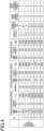
- Fig. 3 shows the thickness T1 (nm) and Young's modulus E1 (GPa) of the first gate insulating coating 21, and the product T1E1 (nm ⁇ GPa) of the thickness T1 and Young's modulus E1 for each of the thin film transistors of Examples 1-1 to 1-20.
- Fig. 3 shows the thickness T2 (nm) and Young's modulus E2 (GPa) of the second gate insulating coating 22, and the product T2E2 (nm . GPa) of the thickness T2 and Young's modulus E2 for each of the thin film transistors of Examples 1-1 to 1-20.
- Fig. 3 shows the thickness T1 (nm) and Young's modulus E1 (GPa) of the first gate insulating coating 21, and the product T1E1 (nm ⁇ GPa) of the thickness T1 and Young's modulus E1 for each of the thin film transistors of Examples 1-1 to 1-20.
- Fig. 3 shows the thickness T2 (nm) and Young
- FIG. 3 further shows the thickness T3 (nm) and Young's modulus E3 (GPa) of the semiconductor layer 13, and the product T3E3 of the thickness T3 and Young's modulus E3 for each of the thin film transistors of Examples 1-1 to 1-20.
- Fig. 3 also shows the mobility, the mobility decrease rate, the number of digits of the on/off ratio before the bending test, and the number of digits of the on/off ratio difference for each of the thin film transistors of Examples 1-1 to 1-20.
- Fig. 4 shows the thickness T1 (nm) and Young's modulus E1 (GPa) of the first gate insulating coating 21, and the product T1E1 (nm GPa) of the thickness T1 and Young's modulus E1 for each of the thin film transistors of Comparative Examples 1-1 to 1-8.
- Fig. 4 shows the thickness T2 (nm) and Young's modulus E2 (GPa) of the second gate insulating coating 22, and the product T2E2 (nm ⁇ GPa) of the thickness T2 and Young's modulus E2 for each of the thin film transistors of Comparative Examples 1-1 to 1-8.
- Fig. 4 shows the thickness T1 (nm) and Young's modulus E1 (GPa) of the first gate insulating coating 21, and the product T1E1 (nm GPa) of the thickness T1 and Young's modulus E1 for each of the thin film transistors of Comparative Examples 1-1 to 1-8.
- Fig. 4 shows the thickness T2 (n
- FIG. 4 further shows the thickness T3 (nm) and Young's modulus E3 (GPa) of the semiconductor layer 13, and the product T3E3 of the thickness T3 and Young's modulus E3 for each of the thin film transistors of Comparative Examples 1-1 to 1-8.
- Fig. 4 also shows the mobility, the mobility decrease rate, the number of digits of the on/off ratio before the bending test, and the number of digits of the on/off ratio difference for each of the thin film transistors of Comparative Examples 1-1 to 1-8.
- the mobilities of the thin film transistors of Examples 1-1 to 1-20 and the mobilities of the thin film transistors of Comparative Examples 1-1 to 1-8 were as high as 10.0 cm 2 /Vs or higher.
- the mobility decrease rates of the thin film transistors of Comparative Examples 1-2 and 1-4 to 1-8 were 50% or higher.
- the mobility decrease rate could not be measured since the thin film transistors were not operable after the bending test.
- the mobility decrease rates of the thin film transistors of Examples 1-17 to 1-20 were as low as 13.0% or lower.
- the mobility decrease rates of the thin film transistors of Examples 1-1 to 1-16 were even lower and had a value of 2.8% or lower.
- the mobility decrease rate can be decreased when the thickness of the first gate insulating coating 21 is within the range of 100 nm or greater and 1500 nm or less, and the product of the thickness and Young's modulus of the first gate insulating coating 21 is within the range of 2000 nm GPa or greater and 30000 nm GPa or less.
- the thickness of the first gate insulating coating 21 was so small that the plasma damage during formation of the second gate insulating coating 22 deteriorated the film quality significantly, and therefore the insulation of the first gate insulating coating 21 decreased when the thin film transistor was bent.
- the thin film transistor of Comparative Example 1-3 it is considered that the Young's modulus of the first gate insulating coating 21 was so low that the plasma damage during formation of the second gate insulating coating 22 deteriorated the film quality significantly, and therefore the insulation of the first gate insulating coating 21 decreased when the thin film transistor was bent.
- the large thickness of the first gate insulating coating 21 increased the strain energy generated in the first gate insulating coating 21 when the thin film transistor was bent, which makes the first gate insulating coating 21 and the second gate insulating coating 22 more prone to cracking when the thin film transistor is bent.
- the adhesion at the interface between the first gate insulating coating 21 and the second gate insulating coating 22 of the thin film transistor of Comparative Example 1-2 decreased.
- the high Young's modulus of the first gate insulating coating 21 made the first gate insulating coating 21 less deformable, which makes the first gate insulating coating 21 and the second gate insulating coating 22 more prone to cracking when the thin film transistor is bent.
- the adhesion at the interface between the first gate insulating coating 21 and the second gate insulating coating 22 of the thin film transistor of Comparative Example 1-4 decreased.
- the mobility decrease rate can be reduced when the thickness of the second gate insulating coating 22 is within the range of 2 nm or greater and 30 nm or less, and the product of the thickness and Young's modulus of the second gate insulating coating 22 is within the range of 100 nm ⁇ GPa or greater and 9000 nm ⁇ GPa or less.
- the thickness of the second gate insulating coating 22 was so small that the film quality of the second gate insulating coating 22 deteriorated and the state of the interface between the second gate insulating coating 22 and the semiconductor layer 13 became unstable. This may be the reason the thin film transistor of Comparative Example 1-5 had a high mobility decrease rate when the thin film transistor was bent.
- the thin film transistor of Comparative Example 1-7 it can be considered that the Young's modulus was so small that the film quality of the second gate insulating coating 22 deteriorated, and the state of the interface between the second gate insulating coating 22 and the semiconductor layer 13 became unstable. This may be the reason the thin film transistor of Comparative Example 1-7 had a high mobility decrease rate when the thin film transistor was bent.
- the large thickness of the second gate insulating coating 22 increased the strain energy generated in the second gate insulating coating 22 when the thin film transistor was bent, which makes the second gate insulating coating 22 more prone to cracking when the thin film transistor is bent.
- the adhesion at the interface between the second gate insulating coating 22 and the first gate insulating coating 21 as well as the adhesion at the interface between the second gate insulating coating 22 and the semiconductor layer 13 decreased in the thin film transistor of Comparative Example 1-6.
- the high Young's modulus of the second gate insulating coating 22 made the second gate insulating coating 22 less deformable, which makes the second gate insulating coating 22 more prone to cracking when the thin film transistor is bent.
- the adhesion at the interface between the second gate insulating coating 22 and the first gate insulating coating 21 as well as the adhesion at the interface between the second gate insulating coating 22 and the semiconductor layer 13 decreased in the thin film transistor of Comparative Example 1-8.
- the mobility decrease rate was able to be reduced since the decrease in film quality, cracking, and deterioration in adhesion were suppressed in both the first gate insulating coating 21 and the second gate insulating coating 22.
- the mobility decrease rate can be further reduced when the thickness of the semiconductor layer 13 is within the range of 15 nm or greater and 50 nm or less, and the product of the thickness and Young's modulus is within the range of 1500 nm ⁇ GPa or greater and 7500 nm ⁇ GPa or less.
- the thin film transistor of Example 1-17 it is considered that the high Young's modulus of the semiconductor layer 13 made the semiconductor layer 13 less deformable, which makes the semiconductor layer 13 more prone to cracking when the thin film transistor is bent. In addition, it is considered that the adhesion at the interface between the second gate insulating coating 22 and the semiconductor layer 13 of the thin film transistor of Example 1-17 is likely to decrease. As for the thin film transistor of Example 1-18, it is considered that the large thickness of the semiconductor layer 13 increased the strain energy generated in the semiconductor layer 13 when the thin film transistor was bent, which makes the semiconductor layer 13 more prone to cracking when the thin film transistor is bent. In addition, it is considered that the adhesion at the interface between the second gate insulating coating 22 and the semiconductor layer 13 of the thin film transistor of Example 1-17 is likely to decrease.
- the thin film transistor of Example 1-19 it can be considered that the Young's modulus was so small that the film quality of the semiconductor layer 13 was likely to deteriorate, and the state of the interface between the second gate insulating coating 22 and the semiconductor layer 13 became unstable. Therefore, the thin film transistor of Example 1-19 may tend to have a high mobility decrease rate when the thin film transistor is bent.
- the thin film transistor of Example 1-20 it can be considered that the thickness of the semiconductor layer 13 was so small that the film quality of the semiconductor layer 13 was likely to deteriorate, and the state of the interface between the second gate insulating coating 22 and the semiconductor layer 13 became unstable. Therefore, the thin film transistor of Example 1-20 may tend to have a high mobility decrease rate when the thin film transistor is bent.
- the mobility decrease rate was able to be further reduced since the decrease in film quality, cracking, and deterioration in adhesion were suppressed in the semiconductor layer 13.
- the number of digits of the on/off ratio before the bending test was nine for the thin film transistors of Examples 1-1 to 1-20 and Comparative Examples 1-1 to 1-8.
- the number of digits of the on/off ratio difference was zero for the thin film transistors of Examples 1-1 to 1-20.
- the number of digits of the on/off ratio difference was five for the thin film transistor of Comparative Examples 1-2, and the number of digits of the on/off ratio difference was six for the thin film transistors of Comparative Examples 1-4, 1-6, and 1-8.
- the number of digits of the on/off ratio difference was two for the thin film transistors of Comparative Examples 1-5 and 1-7.
- a second embodiment of a thin film transistor and an embodiment of a method of manufacturing a thin film transistor will be described below with reference to Figs. 5 to 11 .
- the thin film transistor of the second embodiment differs from the thin film transistor of the first embodiment in that it includes a protective layer.
- the second embodiment will be described focusing on the differences between the first and second embodiments, omitting specific explanation of the components common to the first embodiment by designating the same reference signs thereto as those of the first embodiment.
- Fig. 5 shows a third example of a multilayer structure of a thin film transistor
- Fig. 6 shows a fourth example of a multilayer structure of a thin film transistor.
- the upper and lower surfaces of each component of the thin film transistor will be described assuming it is oriented as in Figs. 5 and 6 .
- a first electrode layer may change its function from source to drain, and a second electrode layer may change its function from drain to source.
- the third example of a thin film transistor is a bottom-gate top-contact transistor.
- the differences of the bottom-gate top-contact transistor structure from the bottom-gate top-contact transistor structure described above, that is, the first example of a thin film transistor will be mainly described below.
- the third example of a thin film transistor has a protective layer 31.
- the protective layer 31 is an insulating layer.
- the protective layer 31 is sandwiched between the semiconductor layer 13, and the source electrode layer 14 and the drain electrode layer 15.
- the protective layer 31 covers the semiconductor layer 13 and part of the second gate insulating coating 22.
- the protective layer 31 has a first through hole 31H1 and a second through hole 31H2.
- the through-holes 31H1 and 31H2 penetrate the protective layer 31 in the thickness direction of the protective layer 31, that is, in the channel depth direction Z.
- An upper surface 13S of the semiconductor layer 13 includes a first region 13S1 and a second region 13S2.
- the first region 13S1 is exposed to the first through hole 31H1 of the protective layer 31.
- the second region 13S2 is exposed to the second through hole 31H2 of the protective layer 31.
- the protective layer 31 covers the semiconductor layer 13 in such a manner that the first and second regions 13S1 and 13S2 on the upper surface 13S of the semiconductor layer 13 are exposed through the protective layer 31.
- the source electrode layer 14 includes a part located on the protective layer 31 and a part filled in the first through hole 31H1.
- the part of the source electrode layer 14 filled in the first through hole 31H1 is in contact with the first region 13S1 of the semiconductor layer 13.
- the drain electrode layer 15 includes a part located on the protective layer 31 and a part filled in the second through hole 31H2.
- the part of the drain electrode layer 15 filled in the second through hole 31H2 is in contact with the second region 13S2 of the semiconductor layer 13.
- the region of the semiconductor layer 13 between the first and second through holes 31H1 and 31H2 is the channel region C.
- the fourth example of a thin film transistor is a bottom-gate top-contact transistor.
- the differences of the bottom-gate top-contact transistor structure from the bottom-gate top-contact transistor structure described above, that is, the first example of a thin film transistor will be mainly described below.
- the fourth example of a thin film transistor has a protective layer 31.
- the protective layer 31 covers part of the semiconductor layer 13.
- the upper surface 13S of the semiconductor layer 13 has a region exposed through the semiconductor layer 13 at each end thereof in the channel length direction X.
- One of the regions exposed from the upper surface 13S of the semiconductor layer 13 is the first region 13S1, and the other is the second region 13S2.
- the protective layer 31 covers the semiconductor layer 13 in such a manner that the first and second regions 13S1 and 13S2 on the upper surface 13S of the semiconductor layer 13 are exposed through the protective layer 31.
- the source electrode layer 14 covers part of the protective layer 31, the first region 13S1 of the semiconductor layer 13, and part of the second gate insulating coating 22.
- the source electrode layer 14 is in contact with the first region 13 S1.
- the drain electrode layer 15 covers part of the protective layer 31, the second region 13S2 of the semiconductor layer 13, and part of the second gate insulating coating 22.
- the drain electrode layer 15 is in contact with the second region 13S2.
- the region of the semiconductor layer 13 covered by the protective layer 31 is the channel region C.
- the protective layer 31 of the present disclosure has a function of protecting the semiconductor layer 13 in the steps of the manufacturing process of the thin film transistor after forming the protective layer 31.
- the source electrode layer 14 and the drain electrode layer 15 are formed after forming the semiconductor layer 13.
- the source electrode layer 14 and the drain electrode layer 15 are formed, for example, by forming metal films for forming the electrode layers 14 and 15 and then etching them.
- wet etching or dry etching is used to etch the metal films.
- an etching solution is used as an etchant for the metal films.
- an etching gas is used as an etchant for the metal films.
- the semiconductor layer 13 may deteriorate as a result of these etchants reacting with the semiconductor layer 13.
- the semiconductor layer 13 Since the semiconductor layer 13 is covered with the protective layer 31 in the step of etching the metal films, the semiconductor layer 13 is prevented from coming into contact with the etchant. This prevents deterioration of the semiconductor layer 13.
- the protective layer 31 has a function of protecting the semiconductor layer 13 from the atmosphere in which the thin film transistor is placed after the thin film transistor is manufactured. Since the semiconductor layer 13 is covered with the protective layer 31 in the thin film transistor, for example, the semiconductor layer 13 is prevented from coming into contact with moisture in the atmosphere. This prevents deterioration of the semiconductor layer 13.
- the material forming the protective layer 31 may be an organic polymer compound or an organic-inorganic composite material.
- the organic polymer compound may be at least one selected from the group consisting of polyvinylphenol, polyimide, polyvinyl alcohol, acrylic polymers, epoxy polymers, fluoropolymers including amorphous fluoropolymers, melamine polymers, furan polymers, xylene polymers, polyamideimide polymers, silicone polymers, and cycloolefin polymers.
- the organic-inorganic composite material may be, for example, a mixture of particles of an organic polymeric compound and inorganic compound.
- particles of an inorganic compound are nanoparticles, that is, particles having a size within the range of several nanometers to several hundreds of nanometers.
- the organic-inorganic composite material may have a molecular structure including an atomic group having the properties of an organic compound and an atomic group having the properties of an inorganic compound.
- An example of such an organic-inorganic composite material is a silsesquioxane.
- the molecular structure of silsesquioxanes has a skeleton formed of silicon and oxygen that is an atomic group having the property of an inorganic compound, and an organic group as an atomic group having the property of an organic compound.
- the protective layer 31 may be a single-layer coating or a multilayer coating.
- the material of each of the layers constituting the protective layer 31 is an organic polymer compound or an organic-inorganic composite material.
- the thickness of the protective layer 31 is preferably 40 nm or greater.
- the protective layer 31 also preferably has a thickness of 40 nm or greater in order to prevent deterioration of the semiconductor layer 13 due to the atmosphere in which the thin film transistor is placed.
- the thickness of the protective layer 31 is preferably 1000 nm or less.
- the surface defining the through holes 31H1 and 31H2 may not be flat if the protective layer 31 is too thick. This may lead to poor conduction between the electrode layers 14 and 15 and the semiconductor layer 13.
- the thickness of the protective layer 31 is particularly preferably within the range of 50 nm or greater and 500 nm or less.
- the resistivity of the protective layer 31 is preferably 1 ⁇ 10 11 ⁇ cm or higher, more preferably 1 ⁇ 10 13 ⁇ cm or higher.
- the Young's modulus of the protective layer 31 is 3 GPa or greater and 20 GPa or less. When the Young's modulus of the protective layer 31 is 3 GPa or greater, deterioration of the film quality of the protective layer 31 is suppressed. When the Young's modulus of the protective layer 31 is 20 GPa or less, deterioration of the bendability of the protective layer 31 is suppressed.
- the Young's modulus of the protective layer 31 is a value measured by a method conforming to ISO14577.
- the protective layer 31 preferably satisfies the following Condition 4.
- the thickness is within the range of 40 nm or greater and 1000 nm or less, and the product of the thickness and Young's modulus is within the range of 120 nm ⁇ GPa or greater and 20000 nm ⁇ GPa or less.
- the protective layer 31 satisfies Condition 4
- deterioration of the film quality and deterioration of bendability of the protective layer 31 are suppressed.
- This prevents the interface between the semiconductor layer 13 and the protective layer 31 from becoming unstable.
- the formation of a leak path between the source electrode layer 14 and the drain electrode layer 15 can be prevented.
- the off current of the thin film transistor can be kept low even when the thin film transistor is bent. This makes it possible to reduce the difference between the on/off ratio of the thin film transistor before being bent and the on/off ratio of the thin film transistor after being bent. As a result, it is possible to further improve the electrical durability of the thin film transistor against bending of the flexible substrate 11.
- the protective layer 31 may be made of silicon oxide, silicon nitride, or silicon oxynitride. In these cases, the Young's modulus of the protective layer 31 falls within the range of 50 GPa or greater and 150 GPa or less. When the Young's modulus of the protective layer 31 is 50 GPa or greater, deterioration of the film quality of the protective layer 31 is suppressed. When the Young's modulus of the protective layer 31 is 150 GPa or less, deterioration of the bendability of the protective layer 31 is suppressed. The Young's modulus of the protective layer 31 is a value measured by a method conforming to ISO14577.
- the protective layer 31 satisfies the following Condition 5.
- the thickness is within the range of 40 nm or greater and 60 nm or less, and the product of the thickness and Young's modulus is within the range of 2000 nm ⁇ GPa or greater and 9000 nm ⁇ GPa or less.
- the interface between the semiconductor layer 13 and the protective layer 31 does not become unstable. As a result, the formation of a leak path between the source electrode layer 14 and the drain electrode layer 15 can be prevented. Since the leakage current between the source electrode layer 14 and the drain electrode layer 15 caused when the thin film transistor is bent is suppressed, the off current of the thin film transistor can be kept low even when the thin film transistor is bent. This makes it possible to reduce the difference between the on/off ratio of the thin film transistor before being bent and the on/off ratio of the thin film transistor after being bent. As a result, it is possible to further improve the electrical durability of the thin film transistor against bending of the flexible substrate 11.
- a method of manufacturing a bottom-gate top-contact transistor includes a first step of forming the gate electrode layer 12 on the flexible substrate 11, a second step of laminating the first gate insulating coating 21 on the gate electrode layer 12, and a third step of laminating the second gate insulating coating 22 on the first gate insulating coating 21.
- the method of manufacturing a bottom-gate top-contact transistor also includes a fourth step of laminating the semiconductor layer 13 on the second gate insulating coating 22, a fifth step of laminating the protective layer 31 on the semiconductor layer 13, and a sixth step of laminating the source electrode layer 14 and the drain electrode layer 15 after forming the protective layer 31.
- the gate electrode layer 12 may be formed with a film formation method using a mask that follows the shape of the gate electrode layer 12.
- the gate electrode layer 12 may be formed by forming an electrode film for forming the gate electrode layer 12 and then processing the electrode film into the shape of the gate electrode layer 12 by etching.
- the film forming method used to form the gate electrode layer 12 may be, for example, at least one selected from the group consisting of vacuum deposition, ion plating, sputtering, laser ablation, spin coating using conductive paste, dip coating, and slit die coating.
- the film forming method used to form the gate electrode layer 12 may be, for example, at least one selected from the group consisting of screen printing, relief printing, intaglio printing, planographic printing, and inkjet printing.
- the first gate insulating coating 21 may be formed by a coating method using a mask that follows the shape of the first gate insulating coating 21.
- the first gate insulating coating 21 may be formed by forming a coating film for forming the first gate insulating coating 21 and then processing the coating film into the shape of the first gate insulating coating 21 by photolithography.
- the coating method used to form the first gate insulating coating 21 may be, for example, at least one selected from the group consisting of spin coating, dip coating, slit die coating, screen printing, gravure offset printing, and inkjet printing, using a coating solution containing an organic polymer compound or an organic-inorganic composite material.
- the coating film is formed by baking a liquid film formed by the coating solution.
- the coating solution contains a photosensitive polymer.
- the second gate insulating coating 22 may be formed by a coating method using a mask that follows the shape of the second gate insulating coating 22.
- the second gate insulating coating 22 may be formed by forming an insulating coating for forming the second gate insulating coating 22 and then processing the coating film into the shape of the second gate insulating coating 22 by etching.
- the film forming method used to form the second gate insulating coating 22 may be, for example, at least one selected from the group consisting of laser ablation, plasma CVD, optical CVD, thermal CVD, sputtering, ALD, and sol-gel.
- the film forming method used to form the second gate insulating coating 22 may be, for example, spin coating, dip coating, slit die coating, screen printing, or inkjet printing, using a coating solution containing a precursor of an inorganic polymer compound.
- the semiconductor layer 13 may be formed with a film formation method using a mask that follows the shape of the semiconductor layer 13.
- the semiconductor layer 13 may be formed by forming a semiconductor coating for forming the semiconductor layer 13 and then processing the semiconductor coating into the shape of the semiconductor layer 13 by etching.
- the semiconductor layer 13 is formed using sputtering, CVD, ALD, or sol-gel.
- Sputtering includes DC sputtering in which a DC voltage is applied to the flexible substrate 11, or RF sputtering in which radio waves are applied to the film forming space.
- the impurities may be, for example, introduced by ion implantation, ion doping, or plasma immersion-ion implantation.
- the film forming method used to form the semiconductor layer 13 may be, for example, spin coating, dip coating, slit die coating, screen printing, or inkjet printing, using a coating solution containing a precursor of an inorganic polymer compound.
- the protective layer 31 may be formed with a coating method that uses a mask that conforms with the shape of the protective layer 31.
- the protective layer 31 may be formed by forming a coating film for forming the protective layer 31 and then processing the coating film into the shape of the protective layer 31 by photolithography.
- the coating method used to form the protective layer 31 may be, for example, at least one selected from the group consisting of spin coating, dip coating, slit die coating, screen printing, and inkjet printing, using a coating solution containing an organic polymer compound or an organic-inorganic composite material.
- the coating film is formed by baking a liquid film formed by the coating solution.
- the coating solution contains a photosensitive polymer.
- the first and second regions 13S1 and 13S2 exposed through the protective layer 31 are formed on the upper surface 13S of the semiconductor layer 13.
- the first region 13S1 is a region connected to the source electrode layer 14.
- the second region 13S2 is a region connected to the drain electrode layer 15.
- the source electrode layer 14 and the drain electrode layer 15 may be formed by a film formation method using a mask that follows the shape of the electrode layer.
- the source electrode layer 14 and the drain electrode layer 15 may be formed by forming electrode coatings for forming the electrode layers 14 and 15 and then processing the electrode coatings into the shape of the source electrode layer 14 and the drain electrode layer 15 by etching.
- the film forming method used to form the source electrode layer 14 and the drain electrode layer 15 may be, for example, at least one selected from the group consisting of vacuum deposition, ion plating, sputtering, laser ablation, spin coating using conductive paste, dip coating, and slit die coating.
- the film forming method used to form the source electrode layer 14 and drain electrode layer 15 may be, for example, screen printing, relief printing, intaglio printing, planographic printing, or inkjet printing.
- Example 2-1 a bottom-gate top-contact transistor having the structure shown in Fig. 5 was obtained.
- a polyimide film having a thickness of 20 ⁇ m was prepared as the flexible substrate 11.
- An AINd film having a thickness of 80 nm was formed as the gate electrode layer 12.
- a resist pattern was formed on the AlNd film by photolithography. Then, the resist pattern was removed from the AlNd film by wet-etching the AlNd film to obtain the gate electrode layer 12.
- the AlNd film forming conditions were as follows.
- an acrylic polymer film having a thickness of 1500 nm was formed as the first gate insulating coating 21.
- a coating film was formed by applying an acrylic solution containing an acrylic polymer, which is an organic polymer compound, to the upper surfaces of the flexible substrate 11 and the gate electrode layer 12 using spin coating. Then, the coating film was baked to obtain an acrylic polymer film as the first gate insulating coating 21.
- the thickness of the first gate insulating coating 21 was measured using a stylus profiler (Dektak 6M, manufactured by Bruker Japan).
- the Young's modulus of the first gate insulating coating 21 was measured using a microhardness tester (TI Premier, manufactured by Bruker Japan). The Young's modulus of the first gate insulating coating 21 was 20 GPa.
- the acrylic polymer film was formed using spin coating under the following conditions.
- a silicon nitride film having a thickness of 30 nm was formed on the upper surface of the acrylic polymer film using a plasma CVD device. Then, a resist pattern was formed on the silicon nitride film by photolithography, and the resist pattern was removed after dry-etching the silicon nitride film to obtain the second gate insulating coating 22.
- the thickness of the second gate insulating coating 22 was measured using the same stylus profilometer as above.
- the Young's modulus of the second gate insulating coating was also measured using the same microhardness tester as above.
- the Young's modulus of the second gate insulating coating 22 was 300 GPa.
- the silicon nitride film was formed using a plasma CVD device under the following conditions.
- an InGaZnO film having a thickness of 50 nm was formed.
- a resist pattern was formed on the InGaZnO film using photolithography.
- the resist pattern was removed by wet-etching the InGaZnO film to obtain the semiconductor layer 13.
- the thickness of the semiconductor layer 13 was measured using the same stylus profilometer as above.
- the Young's modulus of the semiconductor layer 13 was also measured using the same microhardness tester as above.
- the Young's modulus of the semiconductor layer 13 was 150 GPa.
- the InGaZnO film was formed using sputtering under the following conditions.
- a photosensitive acrylic polymer film having a thickness of 40 nm was formed as the protective layer 31.
- a photosensitive acrylic polymer solution containing a photosensitive acrylic polymer, which is an organic polymer compound was diluted four folds with propylene glycol monomethyl ether acetate to prepare the coating solution.
- a coating film was formed by applying the coating solution to the upper surfaces of the semiconductor layer 13 and the second gate insulating coating 22 using spin coating.
- the coating film was patterned using photolithography, and the coating film was baked to obtain a protective layer 31 of a photosensitive acrylic polymer.
- the thickness of the protective layer 31 was measured using the same stylus profilometer as above.
- the Young's modulus of the second gate insulating coating was also measured using the same microhardness tester as above.
- the Young's modulus of the protective layer 31 was 3 GPa.
- the photosensitive acrylic polymer film was formed using spin coating under the following conditions.
- AlNd film forming conditions were as follows.
- the thin film transistor of Example 2-1 was thus obtained.
- the thin film transistor had a channel length of 10 ⁇ m and a channel width of 30 ⁇ m.
- the thin film transistor of Example 2-2 was obtained in the same manner as in Example 2-1 except that the photosensitive acrylic polymer solution was diluted three folds, and the rotational speed of the substrate and the sintering conditions for forming the photosensitive acrylic polymer film were changed as follows.
- the protective layer 31 had a thickness of 50 nm and Young's modulus of 5 GPa.
- the thin film transistor of Example 2-3 was obtained in the same manner as in Example 2-1 except that the photosensitive acrylic polymer solution was diluted three folds, and the rotational speed of the substrate and the sintering conditions for forming the photosensitive acrylic polymer film were changed as follows.
- the protective layer 31 had a thickness of 100 nm and Young's modulus of 10 GPa.
- the thin film transistor of Example 2-4 was obtained in the same manner as in Example 2-1 except that the photosensitive acrylic polymer solution was diluted two folds, and the rotational speed of the substrate and the sintering conditions for forming the photosensitive acrylic polymer film were changed as follows.
- the protective layer 31 had a thickness of 300 nm and Young's modulus of 10 GPa.
- the thin film transistor of Example 2-5 was obtained in the same manner as in Example 2-1 except that the photosensitive acrylic polymer solution was diluted two folds, and the rotational speed of the substrate and the sintering conditions for forming the photosensitive acrylic polymer film were changed as follows.
- the protective layer 31 had a thickness of 500 nm and Young's modulus of 15 GPa.
- the thin film transistor of Example 2-6 was obtained in the same manner as in Example 2-1 except that the photosensitive acrylic polymer solution was diluted two folds, and the rotational speed of the substrate and the sintering conditions for forming the photosensitive acrylic polymer film were changed as follows.
- the protective layer 31 had a thickness of 800 nm and Young's modulus of 15 GPa.
- the thin film transistor of Example 2-7 was obtained in the same manner as in Example 2-1 except that the photosensitive acrylic polymer solution was not diluted, and the rotational speed of the substrate and the sintering conditions for forming the photosensitive acrylic polymer film were changed as follows.
- the protective layer 31 had a thickness of 1000 nm and Young's modulus of 15 GPa.
- the thin film transistor of Example 2-8 was obtained in the same manner as in Example 2-1 except that the photosensitive acrylic polymer solution was not diluted, and the rotational speed of the substrate and the sintering conditions for forming the photosensitive acrylic polymer film were changed as follows.
- the protective layer 31 had a thickness of 1000 nm and Young's modulus of 20 GPa.
- the thin film transistor of Example 2-9 was obtained in the same manner as in Example 1-1 except that the protective layer 31 was changed to a photosensitive cycloolefin polymer film with a thickness of 1000 nm.
- a coating film was formed by applying a photosensitive cycloolefin polymer solution containing a photosensitive cycloolefin polymer, which is an organic polymer compound, to the upper surfaces of the semiconductor layer 13 and the second gate insulating coating 22 by spin coating.
- the coating film was patterned using photolithography, and the coating film was baked to obtain a protective layer 31 of a photosensitive cycloolefin polymer.
- the thickness of the protective layer 31 was measured using the same stylus profilometer as above.
- the Young's modulus of the protective layer 31 was also measured using the same microhardness tester as above.
- the Young's modulus of the protective layer 31 was 20 GPa.
- the photosensitive cycloolefin polymer film was formed using spin coating under the following conditions.
- the thin film transistor of Example 2-10 was obtained in the same manner as in Example 2-8 except that the structure of the thin film transistor was changed to the structure showed in Fig. 6 .
- the thin film transistor of Example 2-11 was obtained in the same manner as in Example 1-1 except that the first gate insulating coating 21 and the protective layer 31 were formed using a photosensitive polymethylsilsesquioxane having a thickness of 500 nm.
- the first gate insulating coating 21 a coating film was formed by applying a precursor solution of a photosensitive polymethylsilsesquioxane, which is an organic-inorganic composite material, to the upper surfaces of the flexible substrate 11 and the gate electrode layer 12 using spin coating.
- the coating film was exposed and developed by photolithography, and then baked to obtain the first gate insulating coating 21 made of a photosensitive polymethylsilsesquioxane film.
- the thickness of the first gate insulating coating 21 was measured using the same stylus profilometer as above.
- the Young's modulus of the first gate insulating coating was also measured using the same microhardness tester as above.
- the Young's modulus of the first gate insulating coating 21 was 20 GPa.
- a coating film was formed by applying a precursor solution of photosensitive polymethylsilsesquioxane, which is an organic-inorganic composite material, to the upper surfaces of the semiconductor layer 13 and the second gate electrode layer 22 using spin coating.
- the coating film was patterned using photolithography, and then baked to obtain a protective layer 31 of photosensitive polymethylsilsesquioxane.
- the thickness of the protective layer 31 was measured using the same stylus profilometer as above.
- the Young's modulus of the protective layer 31 was also measured using the same microhardness tester as above.
- the Young's modulus of the protective layer 31 was 20 GPa.
- the photosensitive polymethylsilsesquioxane film was formed using spin coating under the following conditions.
- the thin film transistor of Example 2-12 was obtained in the same manner as in Example 2-1 except that the first gate insulating coating 21 and the protective layer 31 were changed to a film of an organic-inorganic composite material having a thickness of 500 nm.
- a material in which nanoparticles of silicon oxide are dispersed in an acrylic polymer was used as the organic-inorganic composite material.
- the first gate insulating coating 21 a coating film was formed by applying a solution in which silicon oxide nanoparticles are dispersed in a solution containing an acrylic polymer to the upper surfaces of the flexible substrate 11 and the gate electrode layer 12 using gravure offset printing. Then, the coating film was baked to obtain the first gate insulating coating 21 of an organic-inorganic composite material. The thickness of the first gate insulating coating 21 was measured using the same stylus profilometer as above. The Young's modulus of the first gate insulating coating was also measured using the same microhardness tester as above. The Young's modulus of the first gate insulating coating 21 was 20 GPa.
- a coating film having the pattern of the protective layer 31 was formed by applying a solution in which silicon oxide nanoparticles are dispersed in a solution containing an acrylic polymer to the upper surfaces of the semiconductor layer 13 and the second gate electrode layer 22 using gravure offset printing. Then, the coating film was baked to obtain the protective layer 31 of an acrylic polymer in which silicon oxide nanoparticles are dispersed.
- the thickness of the protective layer 31 was measured using the same stylus profilometer as above.
- the Young's modulus of the protective layer 31 was also measured using the same microhardness tester as above.
- the Young's modulus of the protective layer 31 was 20 GPa.
- the sintering conditions of the acrylic polymer film in which silicon oxide nanoparticles are dispersed are as follows.
- the thin film transistor of Example 2-13 was obtained in the same manner as in Example 2-1 except that the rotation speed of the substrate when forming the photosensitive acrylic polymer film was changed as follows.
- the protective layer 31 had a thickness of 30 nm and Young's modulus of 3 GPa.
- the thin film transistor of Example 2-14 was obtained in the same manner as in Example 2-1 except that the photosensitive acrylic polymer solution forming the protective layer 31 was not diluted, and the rotational speed of the substrate and the sintering conditions for forming the photosensitive acrylic polymer film were changed as follows.
- the protective layer 31 had a thickness of 1200 nm and Young's modulus of 20 GPa.
- the thin film transistor of Example 2-15 was obtained in the same manner as in Example 2-1 except that the rotation speed of the substrate and the sintering conditions in the formation of the photosensitive acrylic polymer film were changed as follows.
- the protective layer 31 had a thickness of 40 nm and Young's modulus of 2 GPa.
- the thin film transistor of Example 2-16 was obtained in the same manner as in Example 2-1 except that the photosensitive acrylic polymer solution forming the protective layer 31 was not diluted, and the rotational speed of the substrate and the sintering conditions for forming the photosensitive acrylic polymer film were changed as follows.
- the protective layer 31 had a thickness of 1000 nm and Young's modulus of 30 GPa.
- the thin film transistor of Example 2-17 was obtained in the same manner as in Example 2-1 except that the protective layer 31 was changed to a silicon oxide film with a thickness of 40 nm.
- a silicon oxide film having a thickness of 40 nm was formed on the upper surfaces of the second gate insulating coating 22 and the semiconductor layer 13 using a plasma CVD device. Then, a resist pattern was formed on the silicon oxide film using photolithography.
- the protective layer 31 was obtained by dry-etching the silicon oxide film and removing the resist pattern from the silicon oxide film. The Young's modulus of the protective layer 31 was 50 GPa.
- the silicon oxide film forming conditions were as follows.
- the thin film transistor of Example 2-18 was obtained in the same manner as in Example 2-1 except that the protective layer 31 was changed to a silicon nitride film with a thickness of 40 nm.
- a silicon nitride film having a thickness of 40 nm was formed on the upper surfaces of the semiconductor layer 13 and the second gate insulating coating 22 using a plasma CVD device. Then, a resist pattern was formed on the silicon nitride film using photolithography.
- the protective layer 31 was obtained by dry-etching the silicon nitride film and removing the resist pattern therefrom.
- the Young's modulus of the protective layer 31 was 150 GPa.
- the silicon nitride film forming conditions were as follows.
- the thin film transistor of Example 2-19 was obtained in the same manner as in Example 2-1 except that the protective layer 31 was formed with a silicon nitride film having a thickness of 60 nm.
- the protective layer 31 To form the protective layer 31, first, a silicon nitride film having a thickness of 60 nm was formed on the upper surfaces of the semiconductor layer 13 and the second gate insulating coating 22 using a plasma CVD device. Then, a resist pattern was formed on the silicon nitride film using photolithography. The silicon nitride film was dry-etched and the resist pattern was removed therefrom. The protective layer 31 was thus obtained.
- the silicon nitride film forming conditions were as follows. The Young's modulus of the protective layer 31 was 150 GPa.
- the thin film transistor of Comparative Example 2-1 was obtained in the same manner as in Example 2-1 except that the protective layer 31 was formed with a silicon oxide film having a thickness of 150 nm.
- the protective layer 31 To form the protective layer 31, first, a silicon oxide film having a thickness of 150 nm was formed on the upper surfaces of the second gate insulating coating 22 and the semiconductor layer 13 using a plasma CVD device. Then, a resist pattern was formed on the silicon oxide film using photolithography. The silicon oxide film was patterned by dry-etching, and the resist pattern was removed therefrom. The protective layer 31 was thus obtained.
- the silicon oxide film forming conditions were as follows. The Young's modulus of the protective layer 31 was 70 GPa.
- the thin film transistor of Comparative Example 2-2 was obtained in the same manner as in Example 2-1 except that the protective layer 31 was formed with a silicon nitride film having a thickness of 80 nm.
- the protective layer 31 To form the protective layer 31, first, a silicon nitride film having a thickness of 80 nm was formed on the upper surfaces of the semiconductor layer 13 and the second gate insulating coating 22 using a plasma CVD device. Then, a resist pattern was formed on the silicon nitride film using photolithography. The silicon nitride film was dry-etched and the resist pattern was removed therefrom. The protective layer 31 was thus obtained.
- the silicon nitride film forming conditions were as follows. The Young's modulus of the protective layer 31 was 150 GPa.
- the transfer characteristics of the thin film transistors of Examples 2-1 to 2-19 and Comparative Examples 2-1 and 2-2 were measured using a semiconductor parameter analyzer (B1500A, manufactured by Agilent Technologies). Then, the mobility and on/off ratio were calculated. The mobility decrease rate and the on/off ratio difference were calculated in the same manner as in the Examples of the first embodiment.
- Fig. 7 shows the thickness T1 (nm) and Young's modulus E1 (GPa) of the first gate insulating coating 21, and the product T1E1 (nm ⁇ GPa) of the thickness T1 and Young's modulus E1 for each of the thin film transistors of Examples 2-1 to 2-19.
- Fig. 7 also shows the thickness T2 (nm) and Young's modulus E2 (GPa) of the second gate insulating coating 22, and the product T2E2 (nm GPa) of the thickness T2 and Young's modulus E2 for each of the thin film transistors of Examples 2-1 to 2-19.
- Fig. 7 shows the thickness T1 (nm) and Young's modulus E1 (GPa) of the first gate insulating coating 21, and the product T1E1 (nm ⁇ GPa) of the thickness T1 and Young's modulus E1 for each of the thin film transistors of Examples 2-1 to 2-19.
- Fig. 7 also shows the thickness T2 (nm) and Young
- FIG. 7 further shows the thickness T4 (nm) and Young's modulus E4 of the protective layer 31, and the product T4E4 (nm GPa) of the thickness T4 and Young's modulus E4 for each of the thin film transistors of Examples 2-1 to 2-19.
- Fig. 8 shows the mobility, the mobility decrease rate, the on/off ratio before the bending test, and the on/off ratio difference for each of the thin film transistors of Examples 2-1 to 2-19.
- Fig. 9 shows the thickness T1 (nm) and Young's modulus E1 (GPa) of the first gate insulating coating 21, and the product T1E1 (nm GPa) of the thickness T1 and Young's modulus E1 for each of the thin film transistors of Comparative Examples 2-1 and 2-2.
- Fig. 9 also shows the thickness T2 (nm) and Young's modulus E2 (GPa) of the second gate insulating coating 22, and the product T2E2 (nm GPa) of the thickness T2 and Young's modulus E2 for each of the thin film transistors of Comparative Examples 2-1 and 2-2.
- Fig. 10 shows the thickness T3 (nm) and Young's modulus E3 (GPa) of the semiconductor layer 13, and the product (T3E3) of the thickness T3 and Young's modulus E3 for each of the thin film transistors of Comparative Examples 2-1 and 2-2.
- Fig. 10 also shows the thickness T4 (nm) and Young's modulus E4 (GPa) of the protective layer 31, and the product (T4E4) of the thickness T4 and Young's modulus E4 for each of the thin film transistors of Comparative Examples 2-1 and 2-2.
- Fig. 11 shows the mobility, the mobility decrease rate, the on/off ratio before the bending test, and the on/off ratio difference for each of the thin film transistors of Comparative Examples 2-1 and 2-2.
- Figs. 7 to 11 show that the mobility before the bending test was within the range of 10.2 or greater and 10.9 or less, and the rate of decrease in mobility after the bending test was within the range of 0.0% or higher and 1.9% or lower for the thin film transistors of Examples 2-1 to 2-19.
- the mobility before the bending test was within the range of 10.3 or greater and 10.5 or less. This means that their mobilities were similar to those of the thin film transistors of Examples.
- the rate of decrease in mobility after the bending test was 69.6% or higher for the thin film transistors of Comparative Examples 2-1 and 2-2, which is significantly higher than the rate of decrease in mobility of the Examples.
- the thin film transistor satisfies Condition 1 described above, the decrease in mobility after the bending test can be suppressed by forming the protective layer 31 with an organic polymer compound or an organic-inorganic composite material. Further, when the thin film transistor satisfies Condition 1, and the protective layer 31 is made of silicon oxide or silicon nitride, the rate of decrease in mobility can be reduced by forming the protective layer 31 so that it satisfies Condition 5 described above.
- the thin film transistor of Comparative Example 2-1 it is considered that the high thickness of the protective layer 31 made the protective layer 31 prone to cracking when the thin film transistor is bent, which deteriorates the semiconductor layer 13 and increases the rate of decrease in mobility.
- the thin film transistor of Comparative Example 2-2 it is considered that the high Young's modulus of the protective layer 31 made the protective layer 31 prone to cracking when the thin film transistor is bent, which deteriorates the semiconductor layer 13 and increases the rate of decrease in mobility.
- the number of digits of the on/off ratio before the bending test was nine for the thin film transistors of Examples 2-1 to 1-16.
- the number of digits of the on/off ratio difference after the bending test was one or less for the thin film transistors of Examples 2-1 to 1-16.
- the number of digits of the on/off ratio before the bending test was nine, and the number of digits of the on/off ratio difference was six or seven.
- the on/off ratio difference before and after the bending test is significantly less than when the protective layer 31 is made of an inorganic compound.
- the protective layer 31 is made of an organic polymer compound or an organic-inorganic composite material, cracking of the protective layer 31, deterioration of the film quality, and destabilization of the interface between the semiconductor layer 13 and the protective layer 31 due to bending of the thin film transistor are less likely to occur, and therefore the on/off ratio difference of the thin film transistor is reduced.
- Fig. 8 shows that the number of digits of the on/off ratio difference was zero for the thin film transistor of Examples 2-1 and 2-12, whereas the number of digits of the on/off ratio difference was one for the thin film transistors of Examples 2-13 to 2-16. That is, when the thickness of the protective layer 31 is within the range of 40 nm or greater and 1000 nm or less, and the product of the thickness and Young's modulus is within the range of 120 nm ⁇ GPa or greater and 20000 nm ⁇ GPa or less, the on/off ratio can be further reduced.
- the high Young's modulus of the protective layer 31 makes the protective layer 31 less deformable. This destabilizes the interface between the protective layer 31 and the semiconductor layer 13 when the thin film transistor is bent and increases the on/off ratio difference.
- the large thickness of the protective layer 31 causes the strain energy generated in the protective layer 31 when the thin film transistor is bent to increase. This destabilizes the interface between the semiconductor layer 13 and the protective layer 31 when the thin film transistor is bent, leading to a large on/off ratio difference.
- the thin film transistor of Example 2-15 it can be considered that the Young's modulus was so small that the film quality of the protective layer 31 was likely to deteriorate, and the state of the interface between the semiconductor layer 13 and the protective layer 31 became unstable. Therefore, the thin film transistor of Example 2-15 tends to have a large on/off ratio difference when the thin film transistor is bent.
- the thin film transistor of Example 2-13 it can be considered that, since the film thickness of the protective layer 31 is not large enough to avoid deterioration of the semiconductor layer 13 in the steps after the formation of the protective layer 31 is formed, the surface of the semiconductor layer 13 is damaged, and the state of the interface between the semiconductor layer 13 and the protective layer 31 becomes unstable. Therefore, the thin film transistor of Example 2-13 tends to have a large on/off ratio difference when the thin film transistor is bent.
- the organic-inorganic composite material may be a mixture of particles of an organic polymer processed product and particles of an inorganic compound, or a substance including an atomic group having the property of an inorganic compound and an atomic group having the property of an organic compound in its molecular structure.
- the thin film transistor includes the protective layer 31 covering the semiconductor layer 13, the protective layer 31 protects the semiconductor layer 13 in the steps after forming the protective layer 31.
- the protective layer 31 also protects the semiconductor layer 13 from the atmosphere in which the thin film transistor is placed after the thin film transistor is manufactured.
Landscapes
- Thin Film Transistor (AREA)
- Formation Of Insulating Films (AREA)
- Electroluminescent Light Sources (AREA)
Abstract
Description
- The present disclosure relates to a thin film transistor including, as a gate insulating layer, a laminate of a first gate insulating coating made of an organic polymer compound or an organic-inorganic composite material and a second gate insulating coating made of an inorganic silicon compound, and a method for manufacturing the thin film transistor.
- A thin film transistor having a gate insulating layer including an organic polymer compound film and an inorganic silicon compound film combines a good withstand voltage and flexibility. When the aim of improving the electrical characteristics of the thin film transistor and improving the adhesion between the layers in the thin film transistor, it has been proposed to control the dielectric property value of the gate insulating layer (= (εA/dA)/(εB/dB)) to 0.015 or higher and 1.0 or lower (for example, see PTL 1). The relative permittivity εA used to calculate the dielectric property value is the relative permittivity of the first gate insulating coating containing the organic polymer compound. The thickness dA is the thickness of the first gate insulating coating. The relative permittivity εB used to calculate the dielectric property value is the relative permittivity of the second gate insulating coating containing the inorganic polymer compound. The thickness dB is the thickness of the second gate insulating coating.
- [PTL 1]
JP 2010-21264 A - The relative permittivity of the gate insulating layer is an index value indicating whether a certain amount of charge induced per unit area can be secured. It is also an index value indicating whether current leakage between the gate electrode and another electrode can be suppressed. Meanwhile, the relative permittivity of the gate insulating layer is not closely related to the electrical durability against bending of the flexible substrate. Similarly, the above-described dielectric property value, which compares the susceptibility to dielectric polarization of the first gate insulating coating to that of the second gate insulating coating, is also not closely related to the electrical durability against bending of the flexible substrate. As a result, when the configuration has a relative permittivity within a predetermined range, or even when the configuration has a dielectric property value within the predetermined range, it may not be possible to increase the electrical durability against bending of the flexible substrate.
- An aspect of a thin film transistor includes a flexible substrate having a support surface; a gate electrode layer located in a first part of the support surface; a gate insulating layer covering a second part of the support surface and the gate electrode layer; a semiconductor layer sandwiching the gate insulating layer with the gate electrode layer; a source electrode layer in contact with a first end of the semiconductor layer with no insulating layer between the source electrode layer and the semiconductor layer; and a drain electrode layer in contact with a second end of the semiconductor layer with no insulating layer between the drain electrode layer and the semiconductor layer. The gate insulating layer includes a first gate insulating coating made of an organic polymer compound or an organic-inorganic composite material and covering the second part and the gate electrode layer, and a second gate insulating coating made of one selected from the group consisting of silicon oxide, silicon nitride, silicon oxynitride, and aluminum oxide. The second gate insulating coating is sandwiched between the first gate insulating coating and a semiconductor layer. The first gate insulating coating has a thickness of 100 nm or greater and 1500 nm or less, and a product of the thickness and Young's modulus of the first gate insulating coating is 300 nm·GPa or greater and 30000 nm·GPa or less. The second gate insulating coating has a thickness of 2 nm or greater and 30 nm or less, and a product of the thickness and Young's modulus of the second gate insulating coating is 100 nm·GPa or greater and 9000 nm·GPa or less.
- An aspect of a method of manufacturing a thin film transistor includes forming a gate electrode layer on a first part of a support surface of a flexible substrate; forming a gate insulating layer covering a second part of the support surface and the gate electrode layer; forming a semiconductor layer sandwiching the gate insulating layer with the gate electrode layer; and forming a source electrode layer in contact with a first end of the semiconductor layer with no insulating layer between the source electrode layer and the semiconductor layer, and a drain electrode layer in contact with a second end of the semiconductor layer with no insulating layer between the drain electrode layer and the semiconductor layer. Forming the gate insulating layer includes forming, by a coating method, a first gate insulating coating made of an organic polymer compound or an organic-inorganic composite material and covering the second part and the gate electrode layer, and forming a second gate insulating coating made of one selected from the group consisting of silicon oxide, silicon nitride, silicon oxynitride, and aluminum oxide, and sandwiched between the first gate insulating coating and the semiconductor layer. The first gate insulating coating has a thickness of 100 nm or greater and 1500 nm or less, and a product of the thickness and Young's modulus of the first gate insulating coating is 300 nm·GPa or greater and 30000 nm·GPa or less. The second gate insulating coating has a thickness of 2 nm or greater and 30 nm or less, and a product of the thickness and Young's modulus of the second gate insulating coating is 100 nm GPa or greater and 9000 nm GPa or less.
- An as aspect of a thin film transistor includes a flexible substrate having a support surface; a gate electrode layer located in a first part of the support surface; a gate insulating layer covering a second part of the support surface and the gate electrode layer; a semiconductor layer sandwiching the gate insulating layer with the gate electrode layer; a protective layer covering the semiconductor layer so that first and second regions on an upper surface of the semiconductor layer are exposed through the protective layer; a source electrode layer in contact with the first region; and a drain electrode layer in contact with the second region. The protective layer is made of an organic polymer compound or an organic-inorganic composite material. The gate insulating layer includes a first gate insulating coating made of an organic polymer compound or an organic-inorganic composite material and covering the second part and the gate electrode layer, and a second gate insulating coating made of one selected from the group consisting of silicon oxide, silicon nitride, silicon oxynitride, and aluminum oxide. The second gate insulating coating is sandwiched between the first gate insulating coating and a semiconductor layer. The first gate insulating coating has a thickness of 100 nm or greater and 1500 nm or less, and a product of the thickness and Young's modulus of the first gate insulating coating is 300 nm·GPa or greater and 30000 nm·GPa or less. The second gate insulating coating has a thickness of 2 nm or greater and 30 nm or less, and a product of the thickness and Young's modulus of the second gate insulating coating is 100 nm GPa or greater and 9000 nm GPa or less.
- An aspect of a method of manufacturing a thin film transistor, includes: forming a gate electrode layer on a first part of a support surface of a flexible substrate; forming a gate insulating layer covering a second part of the support surface and the gate electrode layer; forming a semiconductor layer sandwiching the gate insulating layer with the gate electrode layer; forming a protective layer so that first and second regions on an upper surface of the semiconductor layer are exposed through the protective layer, the protective layer being made of an organic polymer compound or an organic-inorganic composite material; and forming a source electrode layer in contact with the first region, and a drain electrode layer in contact with the second region. Forming the gate insulating layer includes forming, by a coating method, a first gate insulating coating made of an organic polymer compound or an organic-inorganic composite material and covering the second part and the gate electrode layer, and forming a second gate insulating coating made of one selected from the group consisting of silicon oxide, silicon nitride, silicon oxynitride, and aluminum oxide, and sandwiched between the first gate insulating coating and the semiconductor layer. The first gate insulating coating has a thickness of 100 nm or greater and 1500 nm or less, a product of the thickness and Young's modulus of the first gate insulating coating is 300 nm·GPa or greater and 30000 nm·GPa or less, the second gate insulating coating has a thickness of 2 nm or greater and 30 nm or less, and a product of the thickness and Young's modulus of the second gate insulating coating is 100 nm·GPa or greater and 9000 nm·GPa or less.
- An as aspect of a thin film transistor includes a flexible substrate having a support surface; a gate electrode layer located in a first part of the support surface; a gate insulating layer covering a second part of the support surface and the gate electrode layer; a semiconductor layer sandwiching the gate insulating layer with the gate electrode layer; a protective layer covering the semiconductor layer so that first and second regions on an upper surface of the semiconductor layer are exposed through the protective layer; a source electrode layer in contact with the first region; and a drain electrode layer in contact with the second region. The protective layer is made of silicon oxide, silicon nitride, or silicon oxynitride. The gate insulating layer includes a first gate insulating coating made of an organic polymer compound or an organic-inorganic composite material and covering the second part and the gate electrode layer, and a second gate insulating coating made of one selected from the group consisting of silicon oxide, silicon nitride, silicon oxynitride, and aluminum oxide. The second gate insulating coating is sandwiched between the first gate insulating coating and a semiconductor layer. The first gate insulating coating has a thickness of 100 nm or greater and 1500 nm or less, and a product of the thickness and Young's modulus of the first gate insulating coating is 300 nm·GPa or greater and 30000 nm GPa or less. The second gate insulating coating has a thickness of 2 nm or greater and 30 nm or less, and a product of the thickness and Young's modulus of the second gate insulating coating is 100 nm·GPa or greater and 9000 nm·GPa or less. The protective layer has a thickness of 40 nm or greater and 60 nm or less, and a product of the thickness and Young's modulus of the protective layer is 2000 nm·GPa or greater and 9000 nm·GPa or less.
-
-
Fig. 1 is a cross-sectional view showing a first example of a multilayer structure of a thin film transistor according to a first embodiment. -
Fig. 2 is a cross-sectional view showing a second example of the multilayer structure of the thin film transistor according to the first embodiment. -
Fig .3 is a table showing the relationship between the structure of layers, the mobility decrease rate, and the on/off ratio difference for each Example. -
Fig .4 is a table showing the relationship between the structure of layers, the mobility decrease rate, and the on/off ratio difference for each Comparative Example. -
Fig. 5 is a cross-sectional view showing a third example of a multilayer structure of a thin film transistor according to a second embodiment. -
Fig. 6 is a cross-sectional view showing a fourth example of a multilayer structure of a thin film transistor according to the second embodiment. -
Fig. 7 is a table showing the structure of layers of each Example. -
Fig .8 is a table showing the structure of layers, the mobility decrease rate, and the on/off ratio difference of each Example. -
Fig. 9 is a table showing the structure of layers of each Comparative Example. -
Fig. 10 is a table showing the structure of layers of each Comparative Example. -
Fig. 11 is a table showing the structure of layers, the mobility decrease rate, and the on/off ratio difference of each Example. - A first embodiment of a thin film transistor and a method of manufacturing a thin film transistor will be described below. First, the multilayer structure of the thin film transistor will be described, then the constituent materials and dimensions of each layer of the thin film transistor will be described, and finally the method of manufacturing the thin film transistor will be described.
- Note that
Fig. 1 shows a first example of a multilayer structure of a thin film transistor, andFig. 2 shows a second example of a multilayer structure of a thin film transistor. In the following, the upper and lower surfaces of each component of the thin film transistor will be described assuming it is oriented as inFigs. 1 and 2 . - In addition, since the source and the drain in the thin film transistor are determined according to the operation of the driver circuit of the thin film transistor, a first electrode layer may change its function from source to drain, and a second electrode layer may change its function from drain to source.
- As shown in
Fig. 1 , the first example of a thin film transistor is a bottom-gate top-contact transistor. The thin film transistor includes aflexible substrate 11, agate electrode layer 12, a firstgate insulating coating 21, a secondgate insulating coating 22, asemiconductor layer 13, asource electrode layer 14, and adrain electrode layer 15. The firstgate insulating coating 21 and the secondgate insulating coating 22 form a gate insulating layer. - The
flexible substrate 11 and thegate electrode layer 12 are arranged in a channel depth direction Z, which is the upward direction inFig. 1 . Thesource electrode layer 14 and thedrain electrode layer 15 are arranged in a channel length direction X, which is toward the right inFig. 1 . The channel width direction Y is orthogonal to the channel length direction X and the channel depth direction Z. - The upper surface of the
flexible substrate 11 is asupport surface 11S extending in the channel length direction X and the channel width direction Y Thesupport surface 11S includes a first part 11S1 and a second part 11S2 that are in contact with each other in the channel length direction X. The area of the first part 11S1 is less than that of thesecond part 11 S2. The first part 11S1 is in contact with the lower surface of thegate electrode layer 12. The second part 11S2 is in contact with part of the lower surface of the firstgate insulating coating 21. - The first
gate insulating coating 21 is in contact with the upper surface of thegate electrode layer 12. The firstgate insulating coating 21 may either cover theentire support surface 11S or part of thesupport surface 11S. - The lower surface of the second
gate insulating coating 22 is in contact with the upper surface of the firstgate insulating coating 21. The secondgate insulating coating 22 may either cover the entire firstgate insulating coating 21 or part of the firstgate insulating coating 21. The secondgate insulating coating 22 covers the upper surface of thegate electrode layer 12 so that the firstgate insulating coating 21 is sandwiched between the secondgate insulating coating 22 and thegate electrode layer 12. - The lower surface of the
semiconductor layer 13 is in contact with the upper surface of the secondgate insulating coating 22. Thesemiconductor layer 13 covers the upper surface of thegate electrode layer 12 so that the firstgate insulating coating 21 and the secondgate insulating coating 22 are sandwiched between thesemiconductor layer 13 and thegate electrode layer 12. In the channel length direction X, thesemiconductor layer 13 is longer than thegate electrode layer 12. - A first part of the lower surface of the
source electrode layer 14 is in contact with the upper surface of thesemiconductor layer 13. In the channel depth direction Z, there is no insulating layer between thesource electrode layer 14 and thesemiconductor layer 13. A second part of the lower surface of thesource electrode layer 14 is in contact with the upper surface of the secondgate insulating coating 22. Thesource electrode layer 14 covers a first end of thesemiconductor layer 13 so that it is connected to the first end of thesemiconductor layer 13 in the channel length direction X. - A first part of the lower surface of the
drain electrode layer 15 is in contact with the upper surface of thesemiconductor layer 13. In the channel depth direction Z, there is no insulating layer between thedrain electrode layer 14 and thesemiconductor layer 13. A second part of the lower surface of thedrain electrode layer 15 is in contact with the upper surface of the secondgate insulating coating 22. Thedrain electrode layer 15 covers a second end of thesemiconductor layer 13 so that it is connected to the second end of thesemiconductor layer 13 in the channel length direction X. - The
source electrode layer 14 and thedrain electrode layer 15 are separated from each other. A distance L between thesource electrode layer 14 and thedrain electrode layer 15 in the channel length direction X is less than the length of thegate electrode layer 12. In this case, the region of thesemiconductor layer 13 between thesource electrode layer 14 and thedrain electrode layer 15 is a channel region C. The length of the channel region C in the channel length direction X, that is, the distance L between thesource electrode layer 14 and thedrain electrode layer 15 is the channel length. The length of the channel region C in the channel width direction Y is the channel width. - When the channel length of a thin film transistor varies depending on the position in the channel width direction Y, the average value of all the channel lengths is the channel length of that thin film transistor. When the distance L is greater than the length of the
gate electrode layer 12, the channel region C is the region of thesemiconductor layer 13 that overlaps thegate electrode layer 12 in the channel depth direction Z. - As shown in
Fig. 2 , the second example of a thin film transistor is a bottom-gate bottom-contact transistor. The differences of the bottom-gate bottom-contact transistor structure from the bottom-gate top-contact transistor structure will be mainly described below. - The lower surface of the
source electrode layer 14 is in contact with the upper surface of the secondgate insulating coating 22. The lower surface of thedrain electrode layer 15 is in contact with the upper surface of the secondgate insulating coating 22. - A first part of the lower surface of the
semiconductor layer 13 is in contact with the secondgate insulating coating 22. A second part of the lower surface of thesemiconductor layer 13 forms the channel region C filling the gap between thesource electrode layer 14 and thedrain electrode layer 15 in the channel length direction X. - The first end of the
semiconductor layer 13, which is the end of the lower surface thereof in the channel length direction X, covers the upper surface of thesource electrode layer 14 so that the first end is in contact with the upper surface of thesource electrode layer 14. In the channel depth direction Z, there is no insulating layer between thesource electrode layer 14 and thesemiconductor layer 13. The second end of thesemiconductor layer 13, which is the end of the lower surface thereof in the channel length direction X, covers the upper surface of thedrain electrode layer 15 so that the second end is in contact with the upper surface of thedrain electrode layer 15. In the channel depth direction Z, there is no insulating layer between thedrain electrode layer 15 and thesemiconductor layer 13. - The
flexible substrate 11 has an insulating upper surface. Theflexible substrate 11 may be a transparent substrate or an opaque substrate. Theflexible substrate 11 may be an insulating coating, a metal foil having an insulatingsupport surface 11S, an alloy foil having an insulatingsupport surface 11S, or a flexible thin glass plate. - The material forming the
flexible substrate 11 is at least one selected from the group consisting of organic polymer compounds, organic-inorganic composite materials, which are composite materials of organic and inorganic materials, metals, alloys, and inorganic polymer compounds. - The
flexible substrate 11 may have a single-layer structure or a multilayer structure. When theflexible substrate 11 has a multilayer structure, the material of each of the layers forming theflexible substrate 11 is one selected from the group consisting of organic polymer compounds, composite materials, metals, alloys, and inorganic polymer compounds. - When the
flexible substrate 11 has a multilayer structure, theflexible substrate 11 may include a base substrate and a release layer that can be peeled off from the base substrate. The release layer is peeled off from the base substrate together with the device structure. The release layer provided with the device structure may be attached to another flexible substrate. Examples of flexible substrates include paper with low heat resistance, cellophane substrates, cloth, recycled fibers, leather, nylon substrates, and polyurethane substrates. In this example, the release layer and the flexible substrate forms anotherflexible substrate 11. - The organic polymer compound is at least one selected from the group consisting of polymethyl methacrylate, polyacrylate, polycarbonate, polystyrene, polyethylene sulfide, polyether sulfone, polyolefin, polyethylene terephthalate, polyethylene naphthalate, cycloolefin polymer, polyether sulphene, triacetyl cellulose, polyvinyl fluoride, ethylene-tetrafluoroethylene copolymers, polyimide, fluorine polymers, and cyclic polyolefin polymers.
- The composite material is a glass fiber reinforced acrylic polymer or glass fiber reinforced polycarbonate. The metal is aluminum or copper. The alloy is an iron-chromium alloy, an iron-nickel alloy, or an iron-nickel-chromium alloy. The inorganic polymer compound is an alkali-free glass or alkali glass. Alkali-free glass includes silicon oxide, boron oxide, and aluminum oxide. Alkali glass includes silicon oxide, sodium oxide, and calcium oxide.
- The electrode layers 12, 14, and 15 may have a single-layer structure or a multilayer structure. When the electrode layers 12, 14, and 15 have a multilayer structure, each of them preferably includes a bottom layer for enhancing the adhesion with the layer below the
electrode layer electrode layer - The material of each
electrode layer - The metal is at least one of transition metals, alkali metals, and alkaline earth metals. The transition metal is at least one selected from the group consisting of indium, aluminum, gold, silver, platinum, titanium, copper, nickel, and tungsten. The alkali metal is lithium or cesium. The alkaline earth metal is at least one of magnesium and calcium. The alloy is one selected from the group consisting of molybdenum-niobium (MoNb), iron-chromium, aluminum-lithium, magnesium-silver, aluminum-neodymium alloy, and aluminum-neodymium-zirconia alloy.
- The metal oxide is one selected from the group consisting of indium oxide, tin oxide, zinc oxide, cadmium oxide, indium cadmium oxide, cadmium tin oxide, and zinc tin oxide. The metal oxide may contain impurities. The metal oxide containing impurities is indium oxide containing at least one impurity selected from the group consisting of tin, zinc, titanium, cerium, hafnium, zirconia, and molybdenum. The metal oxide containing impurities may be tin oxide containing antimony or fluorine. The metal oxide containing impurities may be zinc oxide containing at least one impurity selected from the group consisting of gallium, aluminum, and boron.
- When the material forming the
semiconductor layer 13 is a metal oxide, the electrode layers 14 and 15 may be made of the same constituent elements as thesemiconductor layer 13 and have an impurity concentration sufficiently higher than that of thesemiconductor layer 13. - In order to expand the range of materials that can be applied to the electrode layers 12, 14, and 15, the electrical resistivity of the electrode layers 12, 14, and 15 is preferably 5.0×10⁻⁵ Ω·cm or higher. In order to suppress the power consumption of the thin film transistor, the electrical resistivity of the electrode layers 12, 14, and 15 is preferably 1.0×10⁻² Ω·cm or lower.
- In order to suppress the electric resistance of the electrode layers 12, 14, and 15, the thickness of each of the electrode layers 12, 14, and 15 is preferably 50 nm or greater. In order to improve the flatness of the layers constituting the thin film transistor, the thickness of each of the electrode layers 12, 14, and 15 is preferably 300 nm or less.
- The material forming the first
gate insulating coating 21 is, for example, an organic polymer compound. The organic polymer compound is at least one selected from the group consisting of polyvinylphenol, polyimide, polyvinyl alcohol, acrylic polymers, epoxy polymers, fluoropolymers including amorphous fluoropolymers, melamine polymers, furan polymers, xylene polymers, polyamideimide polymers, silicone polymers, and cycloolefin polymers. In order to increase the heat resistance of the firstgate insulating coating 21, the organic polymer compound is preferably at least one selected from the group consisting of polyimide, acrylic polymers, and fluorine polymers. - The material forming the first
gate insulating coating 21 may be an organic-inorganic composite material. The organic-inorganic composite material may be, for example, a mixture of particles of an organic polymeric compound and inorganic compound. Note that particles of an inorganic compound are nanoparticles, that is, particles having a size within the range of several nanometers to several hundreds of nanometers. - Alternatively, the organic-inorganic composite material may have a molecular structure including an atomic group having the properties of an organic compound and an atomic group having the properties of an inorganic compound. An example of such an organic-inorganic composite material is a silsesquioxane. The molecular structure of silsesquioxanes has a skeleton formed of silicon and oxygen that is an atomic group having the property of an inorganic compound, and an organic group as an atomic group having the property of an organic compound.
- An organic-inorganic composite material can combine the properties of an organic polymer compound and the properties of an inorganic compound. Therefore, for example, an organic-inorganic composite material can combine flex resistance and impact resistance, which are characteristics of organic polymer compounds, with heat resistance and durability, which are characteristics of inorganic compounds.
- The first
gate insulating coating 21 may be a single layer coating or a multilayer coating. When the firstgate insulating coating 21 is a multilayer coating, the material of each of the layers constituting the firstgate insulating coating 21 is an organic polymer compound or an organic-inorganic composite material. - In order to suppress current leakage between the
gate electrode layer 12 and the other electrode layers 14 and 15, the thickness of the firstgate insulating coating 21 is preferably 100 nm or greater. In order to reduce the gate voltage for driving the thin film transistor, the thickness of the firstgate insulating coating 21 is preferably 1500 nm or less. Further, in order to improve the effectiveness of obtaining these effects, improve the uniformity of the thickness of the firstgate insulating coating 21, and improve the productivity of the firstgate insulating coating 21, the thickness of the firstgate insulating coating 21 is more preferably 400 nm or greater and 1000 nm or less. - The Young's modulus of the first
gate insulating coating 21 is 3 GPa or greater and 20 GPa or less. When the Young's modulus of the firstgate insulating coating 21 is 3 GPa or greater, deterioration of the film quality of the firstgate insulating coating 21 is suppressed, which in turn suppresses a decrease in withstand voltage. When the Young's modulus of the firstgate insulating coating 21 is 20 GPa or less, deterioration of the bendability of the firstgate insulating coating 21 is suppressed. The Young's modulus of the firstgate insulating coating 21 is a value measured by a method conforming to ISO 14577. - In order to secure sufficient insulation between the
gate electrode layer 12 and thesource electrode layer 14, and sufficient insulation between the gate electrode layer 23 and thedrain electrode layer 15, the resistivity of the firstgate insulating coating 21 is preferably 1 × 10¹¹ Ω·cm or higher, more preferably 1 × 10¹³ Ω·cm or higher. - The material forming the second
gate insulating coating 22 is, for example, an inorganic silicon compound having no long-range order. The inorganic silicon compound is at least one selected from the group consisting of silicon oxide, silicon nitride, and silicon oxynitride. Elements constituting silicon oxide include oxygen, silicon, and hydrogen. Elements constituting silicon nitride include nitrogen, silicon, and hydrogen. Elements constituting silicon oxynitride include oxygen, nitrogen, silicon, and hydrogen. The material forming the secondgate insulating coating 22 may be aluminum oxide. Elements constituting aluminum oxide include oxygen and aluminum. - The second
gate insulating coating 22 may be a single-layer coating or a multilayer coating. When the secondgate insulating coating 22 is a multilayer film, the material of each of the layers forming the secondgate insulating coating 22 is one selected from the group consisting of silicon oxide, silicon nitride, silicon oxynitride, and aluminum oxide. The secondgate insulating coating 22 preferably has a resistivity of 1 × 10¹¹ Q or higher, more preferably 1 × 10¹³ Q or higher. - The Young's modulus of the second
gate insulating coating 22 is 50 GPa or greater and 300 GPa or less. When the Young's modulus of the secondgate insulating coating 22 is 50 GPa or greater, deterioration of the film quality of the secondgate insulating coating 22 is suppressed, which in turn suppresses a decrease in mobility in the thin film transistor. When the Young's modulus of the secondgate insulating coating 22 is 300 GPa or less, deterioration of the flex resistance is suppressed. Similarly to the Young's modulus of the firstgate insulating coating 21, the Young's modulus of the secondgate insulating coating 22 is a value measured by a method conforming to ISO14577. - The thin film transistor of the present disclosure satisfies the following
Conditions
(Condition 1) The thickness of the firstgate insulating coating 21 is within the range of 100 nm or greater and 1500 nm or less, and the product of the thickness and Young's modulus of the firstgate insulating coating 21 is within the range of 300 nm·GPa or greater and 30000 nm·GPa or less. - (Condition 2) The thickness of the second
gate insulating coating 22 is within the range of 2 nm or greater and 30 nm or less, and the product of the thickness and Young's modulus of the secondgate insulating coating 22 is within the range of 100 nm·GPa or greater and 9000 nm·GPa or less. - When the first
gate insulating coating 21 satisfiesCondition 1, deterioration of the film quality of the firstgate insulating coating 21 is suppressed, which in turn suppresses a decrease in withstand voltage due to bending. In particular, in cases where the secondgate insulating coating 22 is formed by a film formation method using plasma, the effect of plasma damage on the film quality of the firstgate insulating coating 21 is suppressed, which in turn suppresses a decrease in insulation due to bending. - In addition, when the first
gate insulating coating 21 satisfiesCondition 1, it is possible to suppress an increase in the strain energy generated in the firstgate insulating coating 21 when it is bent and a decrease in the deformability of the firstgate insulating coating 21. This prevents the firstgate insulating coating 21 and the secondgate insulating coating 22 from cracking and the adhesion between the firstgate insulating coating 21 and the secondgate insulating coating 22 deteriorating. - When the second
gate insulating coating 22 satisfiesCondition 2, deterioration of the film quality of the secondgate insulating coating 22 is suppressed, which in turn prevents the state of the interface between the secondgate insulating coating 22 and thesemiconductor layer 13 becoming unstable. When the thickness of the secondgate insulating coating 22 is 2 nm or greater, scattered islands of the secondgate insulating coating 22 will not be formed. This ensures formation of a continuous coating. - In addition, when the second
gate insulating coating 22 satisfiesCondition 2, it is possible to suppress an increase in the strain energy generated in the secondgate insulating coating 22 when it is bent and a decrease in the deformability of the secondgate insulating coating 22. This prevents the adhesion between the secondgate insulating coating 22 and thesemiconductor layer 13 deteriorating. - Thus, when the first
gate insulating coating 21 satisfiesCondition 1 and the secondgate insulating coating 22 satisfiesCondition 2, even when the thin film transistor is bent, the firstgate insulating coating 21 and the secondgate insulating coating 22 themselves do not deteriorate, and also the state of the interface between the firstgate insulating coating 21 and the secondgate insulating coating 22 does not deteriorate. This reduces the decrease in mobility caused by the thin film transistor being bent. As a result, it is possible to improve the electrical durability of the thin film transistor against bending of the flexible substrate. - The material of the
semiconductor layer 13 may be an inorganic semiconductor or an organic semiconductor. The inorganic semiconductor may be an oxide semiconductor, non-monocrystalline silicon, or a compound semiconductor. The non-monocrystalline silicon may be amorphous silicon or polycrystalline silicon. The oxide semiconductor contains at least one of indium and zinc. - In order to increase the light transmittance and field-effect mobility (hereinafter also referred to as mobility) of the
semiconductor layer 13, thesemiconductor layer 13 is preferably an amorphous oxide semiconductor layer containing indium. The oxide semiconductor is more preferably an In-M-Zn oxide. An In-M-Zn oxide contains indium (In) and zinc (Zn), and also includes at least one metal element (M) selected from the group consisting of aluminum, titanium, gallium (Ga), germanium, yttrium, zirconium, lanthanum, cerium, hafnium, and tin. - In order to improve the uniformity of the thickness of the
semiconductor layer 13, the thickness of thesemiconductor layer 13 is preferably 15 nm or greater. In order to reduce the amount of material for forming thesemiconductor layer 13, the thickness of thesemiconductor layer 13 is preferably 100 nm or less. In order to achieve both improved thickness uniformity and reduced amount of material used, the thickness of thesemiconductor layer 13 is preferably 15 nm or greater and 100 nm or less. Further, in order to enhance the effectiveness of obtaining these effects, the thickness of thesemiconductor layer 13 is more preferably 15 nm or greater and 50 nm or less. - In order to increase the mobility in the thin film transistor, the conductivity of the semiconductor layer is preferably 1.0×10⁻⁷ S/cm or higher and 1.0×10⁻¹ S/cm or lower.
- The Young's modulus of the
semiconductor layer 13 is preferably 100 GPa or greater and 150 GPa or less. When the Young's modulus of thesemiconductor layer 13 is 100 GPa or greater, deterioration of the film quality of thesemiconductor layer 13 is suppressed, which in turn suppresses a decrease in mobility in the thin film transistor. When the Young's modulus of thesemiconductor layer 13 is 150 GPa or less, deterioration of the flex resistance is suppressed. Similarly to the Young's modulus of the firstgate insulating coating 21, the Young's modulus of thesemiconductor layer 13 is a value measured by a method conforming to ISO14577. - The
semiconductor layer 13 preferably satisfies the followingCondition 3. - (Condition 3) The thickness of the
semiconductor layer 13 is within the range of 15 nm or greater and 50 nm or less, and the product of the thickness and Young's modulus is within the range of 1500 nm·GPa or greater and 7500 nm·GPa or less. - When the
semiconductor layer 13 satisfiesCondition 3, deterioration of the film quality of thesemiconductor layer 13 is suppressed, which in turn prevents the interface between thesemiconductor layer 13 and the secondgate insulating coating 22 from becoming unstable. In addition, when thesemiconductor layer 13 satisfiesCondition 3, it is possible to suppress an increase in the strain energy generated in thesemiconductor layer 13 when it is bent and a decrease in the deformability of thesemiconductor layer 13. This prevents the adhesion between thesemiconductor layer 13 and the secondgate insulating coating 22 deteriorating. As a result, the decrease in mobility caused by the thin film transistor being bent can be further reduced. - Accordingly, when the
semiconductor layer 13 satisfiesCondition 3, it is possible to prevent thesemiconductor layer 13 itself from deteriorating and the state of the interface between thesemiconductor layer 13 and the secondgate insulating coating 22 deteriorating when the thin film transistor is bent. This further reduces the decrease in mobility due to bending of the thin film transistor. As a result, it is possible to further improve the electrical durability of the thin film transistor against bending of the flexible substrate. - A method of manufacturing a bottom-gate top-contact transistor includes a first step of forming the
gate electrode layer 12 on theflexible substrate 11, a second step of laminating the firstgate insulating coating 21 on thegate electrode layer 12, and a third step of laminating the secondgate insulating coating 22 on the firstgate insulating coating 21. The method of manufacturing a bottom-gate top-contact transistor also includes a fourth step of laminating thesemiconductor layer 13 on the secondgate insulating coating 22, and a fifth step of laminating thesource electrode layer 14 and thedrain electrode layer 15 on thesemiconductor layer 13. - Note that, in a method of manufacturing a bottom-gate bottom-contact transistor, in the fourth step, the
source electrode layer 14 and thedrain electrode layer 15 are laminated on the secondgate insulating coating 22. In the fifth step, thesemiconductor layer 13 is laminated on thesource electrode layer 14, thedrain electrode layer 15, and the secondgate insulating coating 22. In the fourth step, the method used in the fifth step of the method of manufacturing a bottom-gate top-contact transistor is used. In the fifth step, the method used in the fourth step of the method of manufacturing a bottom-gate top-contact transistor is used. Therefore, the method of manufacturing a bottom-gate top-contact transistor will be mainly described below, and redundant description of the method of manufacturing a bottom-gate bottom-contact transistor will be omitted. - In the first step, the
gate electrode layer 12 may be formed with a film formation method using a mask that follows the shape of thegate electrode layer 12. Alternatively, thegate electrode layer 12 may be formed by forming an electrode film for forming thegate electrode layer 12 and then processing the electrode film into the shape of thegate electrode layer 12 by etching. - The film forming method used to form the
gate electrode layer 12 may be, for example, at least one selected from the group consisting of vacuum deposition, ion plating, sputtering, laser ablation, spin coating using conductive paste, dip coating, and slit die coating. Alternatively, the film forming method used to form thegate electrode layer 12 may be, for example, at least one selected from the group consisting of screen printing, relief printing, intaglio printing, planographic printing, and inkjet printing. - In the second step, the first
gate insulating coating 21 may be formed by a coating method using a mask that follows the shape of the firstgate insulating coating 21. Alternatively, the firstgate insulating coating 21 may be formed by forming a coating film for forming the firstgate insulating coating 21 and then processing the coating film into the shape of the firstgate insulating coating 21 by photolithography. - The coating method used to form the first
gate insulating coating 21 may be, for example, at least one selected from the group consisting of spin coating, dip coating, slit die coating, screen printing, gravure offset printing, and inkjet printing, using a coating solution containing an organic polymer compound, an organic-inorganic composite material, or a precursor of an organic-inorganic composite material. In the coating method, the coating film is formed by baking a liquid film formed by the coating solution. When photolithography is used to form the firstgate insulating coating 21, the coating solution contains a photosensitive polymer. - In the third step, the second
gate insulating coating 22 may be formed by a coating method using a mask that follows the shape of the secondgate insulating coating 22. Alternatively, the secondgate insulating coating 22 may be formed by forming an insulating coating for forming the secondgate insulating coating 22 and then processing the coating film into the shape of the secondgate insulating coating 22 by etching. - The film forming method used to form the second
gate insulating coating 22 may be, for example, at least one selected from the group consisting of laser ablation, plasma CVD, optical CVD, thermal CVD, sputtering, ALD, and sol-gel. Alternatively, the film forming method used to form the secondgate insulating coating 22 may be, for example, at least one coating method selected from the group consisting of spin coating, dip coating, slit die coating, screen printing, and inkjet printing, using a coating solution containing a precursor of an inorganic polymer compound. - In the fourth step, the
semiconductor layer 13 may be formed with a film formation method using a mask that follows the shape of thesemiconductor layer 13. Alternatively, thesemiconductor layer 13 may be formed by forming a semiconductor coating for forming thesemiconductor layer 13 and then processing the semiconductor coating into the shape of thesemiconductor layer 13 by etching. - The
semiconductor layer 13 is formed using sputtering, CVD, ALD, or sol-gel. Sputtering includes DC sputtering in which a DC voltage is applied to theflexible substrate 11, or RF sputtering in which radio waves are applied to the film forming space. The impurities may be, for example, introduced by ion implantation, ion doping, or plasma immersion-ion implantation. Alternatively, the film forming method used to form thesemiconductor layer 13 may be, for example, at least one coating method selected from the group consisting of spin coating, dip coating, slit die coating, screen printing, and inkjet printing, using a coating solution containing a precursor of an inorganic polymer compound. - In the fifth step, the
source electrode layer 14 and thedrain electrode layer 15 may be formed by a film formation method using a mask that follows the shape of the electrode layer. Alternatively, thesource electrode layer 14 and thedrain electrode layer 15 may be formed by forming electrode coatings for forming the electrode layers 14 and 15 and then processing the electrode coatings into the shape of thesource electrode layer 14 and thedrain electrode layer 15 by etching. - The film forming method used to form the
source electrode layer 14 and thedrain electrode layer 15 is at least one selected from the group consisting of vacuum deposition, ion plating, sputtering, laser ablation, spin coating using conductive paste, dip coating, and slit die coating. Alternatively, the film forming method used to form thesource electrode layer 14 anddrain electrode layer 15 may be, for example, at least one selected from the group consisting of screen printing, relief printing, intaglio printing, planographic printing, and inkjet printing. - In Example 1-1, a bottom-gate top-contact transistor having the structure shown in
Fig. 1 was obtained. - First, a polyimide film having a thickness of 20 µm was prepared as the
flexible substrate 11. An AINd film having a thickness of 80 nm was formed as thegate electrode layer 12. After forming the AlNd film at room temperature using a DC magnetron sputtering system, a resist pattern was formed on the AlNd film by photolithography. Then, the resist pattern was removed from the AlNd film by wet-etching the AlNd film to obtain thegate electrode layer 12. The AlNd film forming conditions were as follows. -
- Target composition ratio: Al (at%):Nd (at%) = 98:2
- Sputtering gas: Argon
- Sputtering gas flow rate: 100 sccm
- Film formation pressure: 1.0 Pa
- Target power: 200 W (DC)
- Substrate temperature: Room temperature
- Subsequently, an acrylic polymer film having a thickness of 1500 nm was formed as the first
gate insulating coating 21. In the formation of the acrylic polymer film, first, a coating film was formed by applying an acrylic solution containing an acrylic polymer, which is an organic polymer compound, to the upper surfaces of theflexible substrate 11 and thegate electrode layer 12 using spin coating. Then, the coating film was baked to obtain an acrylic polymer film. - After that, the thickness of the first
gate insulating coating 21 was measured using a stylus profiler (Dektak 6M, manufactured by Bruker Japan). In addition, the Young's modulus of the firstgate insulating coating 21 was measured using a microhardness tester (TI Premier, manufactured by Bruker Japan). The Young's modulus of the firstgate insulating coating 21 was 20 GPa. - The acrylic polymer film was formed using spin coating under the following conditions.
-
- Substrate rotation speed: 420 rpm/30 sec
- Sintering temperature: 220°C
- Sintering time: 1 hour
- A silicon nitride film having a thickness of 30 nm was formed on the upper surface of the acrylic polymer film using a plasma CVD device. Then, a resist pattern was formed on the silicon nitride film by photolithography, and the resist pattern was removed after dry-etching the silicon nitride film to obtain the second
gate insulating coating 22. The thickness of the secondgate insulating coating 22 was measured using the same stylus profilometer as above. The Young's modulus of the second gate insulating coating was also measured using the same microhardness tester as above. The Young's modulus of the secondgate insulating coating 22 was 300 GPa. - The silicon nitride film was formed using a plasma CVD device under the following conditions.
-
- Reactive gas: Silane/ammonia/hydrogen/nitrogen
- Reactive gas flow rate: 10 sccm (silane), 70 sccm (ammonia)
5000 sccm (hydrogen), 2000 sccm (nitrogen) - Film formation pressure: 200 Pa
- Radio wave power: 1000 W
- Radio wave power frequency: 13.56 MHz
- Substrate temperature: 200°C
- Film formation time: 90 sec
- Subsequently, using a DC magnetron sputtering system, an InGaZnO film having a thickness of 50 nm was formed. Next, a resist pattern was formed on the InGaZnO film using photolithography. Then, the resist pattern was removed by wet-etching the InGaZnO film to obtain the
semiconductor layer 13. The thickness of thesemiconductor layer 13 was measured using the same stylus profilometer as above. The Young's modulus of thesemiconductor layer 13 was also measured using the same microhardness tester as above. The Young's modulus of thesemiconductor layer 13 was 150 GPa. - The InGaZnO film was formed using sputtering under the following conditions.
-
- Target composition ratio: at% In:Ga:Zn:O = 1:1:1:4
- Sputtering gas: Argon/oxygen
- Sputtering gas flow rate: 50 sccm (argon), 0.2 sccm (oxygen)
- Film formation pressure: 1.0 Pa
- Target power: 450W • Target frequency: 13.56MHz
- Substrate temperature: Room temperature
- Film formation time: 25 min
- Subsequently, a lift-off resist was applied onto the
semiconductor layer 13 and the secondgate insulating coating 22 using a spin coater. Then, an inverted pattern of thesource electrode layer 14 and thedrain electrode layer 15 was formed from the lift-off resist using photolithography. Subsequently, using a DC magnetron sputtering system, an AlNd film having a thickness of 80 nm was formed at room temperature. The inverted pattern was removed using the lift-off method to obtain thesource electrode layer 14 and thedrain electrode layer 15. The thin film transistor of Example 1-1 was thus obtained. The thin film transistor had a channel length of 10 µm and a channel width of 30 µm. - The AlNd film was formed using sputtering under the following conditions.
-
- Target composition ratio: Al (at%):Nd (at%) = 98:2
- Sputtering gas: Argon
- Sputtering gas flow rate: 100 sccm
- Film formation pressure: 1.0 Pa
- Target power: 200 W (DC)
- Substrate temperature: Room temperature
- The thin film transistor of Example 1-2 was obtained in the same manner as in Example 1-1 except that the spin coating conditions for forming the first
gate insulating coating 21 were changed as follows and the sintering temperature was changed to 200°C. The firstgate insulating coating 21 had a thickness of 1500 nm and Young's modulus of 10 GPa. - The thin film transistor of Example 1-2 was obtained in the same manner as in Example 1-1 except that the spin coating conditions for forming the first
gate insulating coating 21 were changed as follows. The firstgate insulating coating 21 had a thickness of 700 nm and Young's modulus of 20 GPa. - The thin film transistor of Example 1-4 was obtained in the same manner as in Example 1-1 except that the spin coating conditions for forming the first
gate insulating coating 21 were changed as follows and the sintering temperature of the firstgate insulating coating 21 was changed to 180°C. The firstgate insulating coating 21 had a thickness of 1500 nm and Young's modulus of 3 GPa. - The thin film transistor of Example 1-5 was obtained in the same manner as in Example 1-1 except that the acrylic polymer solution for forming the first
gate insulating coating 21 was diluted three folds using propylene glycol monomethyl ether acetate as the dilution solvent, and the spin coating conditions were changed as follows. The firstgate insulating coating 21 had a thickness of 100 nm and Young's modulus of 20 GPa. - The thin film transistor of Example 1-6 was obtained in the same manner as in Example 1-1 except that the second
gate insulating coating 22 was formed with an aluminum oxide film formed using an ALD device. The secondgate insulating coating 22 had a thickness of 30 nm and Young's modulus of 250 GPa. - The aluminum oxide film was formed using an ALD device under the following conditions.
-
- Reactive gas: Trimethylaluminum/water vapor
- Purge gas: Nitrogen
- Film formation pressure: 40 Pa
- Number of cycles: 330 times
- Substrate temperature: 200°C
- The thin film transistor of Example 1-7 was obtained in the same manner as in Example 1-1 except that the second
gate insulating coating 22 was formed with a silicon oxynitride film formed using a plasma CVD device. The secondgate insulating coating 22 had a thickness of 30 nm and Young's modulus of 150 GPa. - The silicon oxynitride film was formed using a plasma CVD device under the following conditions.
-
- Reactive gas: Silane/ammonia/hydrogen/nitrous oxide
- Reactive gas flow rate: 50 sccm (silane), 100 sccm (ammonia)
- 1000 sccm (hydrogen)
- 500 sccm (dinitrogen monoxide)
- Film formation pressure: 300 Pa
- Radio wave power: 900 W
- Radio wave power frequency: 13.56 MHz
- Substrate temperature: 200°C
- Film formation time: 110 sec
- The thin film transistor of Example 1-8 was obtained in the same manner as in Example 1-1 except that the film formation time in the formation of the second
gate insulating coating 22 was changed to 30 seconds. The secondgate insulating coating 22 had a thickness of 10 nm and Young's modulus of 300 GPa. - The thin film transistor of Example 1-9 was obtained in the same manner as in Example 1-1 except that the second
gate insulating coating 22 was formed with a silicon oxide film formed using a plasma CVD device. The secondgate insulating coating 22 had a thickness of 30 nm and Young's modulus of 50 GPa. - The silicon oxide film was formed using a plasma CVD device under the following conditions.
-
- Reactive gas: Silane/nitrous oxide
- Reactive gas flow rate: 65 sccm (silane)
500 sccm (dinitrogen monoxide) - Film formation pressure: 200 Pa
- Radio wave power: 500 W
- Radio wave power frequency: 13.56 MHz
- Substrate temperature: 200°C
- Film formation time: 120 sec
- The thin film transistor of Example 1-10 was obtained in the same manner as in Example 1-1 except that the film formation time in the formation of the second
gate insulating coating 22 was changed to 6 seconds. The secondgate insulating coating 22 had a thickness of 2 nm and Young's modulus of 300 GPa. - The thin film transistor of Example 1-11 was obtained in the same manner as in Example 1-9 except that the film formation time in the formation of the second
gate insulating coating 22 was changed to 8 seconds. The secondgate insulating coating 22 had a thickness of 2 nm and Young's modulus of 50 GPa. - The thin film transistor of Example 1-12 was obtained in the same manner as in Example 1-1 except that the target power in the formation of the
semiconductor layer 13 was changed to 350 W and the film formation time was changed to 35 minutes. The secondgate insulating coating 22 had a thickness of 30 nm and Young's modulus of 300 GPa. Thesemiconductor layer 13 had a thickness of 50 nm and Young's modulus of 120 GPa. - The thin film transistor of Example 1-13 was obtained in the same manner as in Example 1-1 except that the target power in the formation of the
semiconductor layer 13 was changed to 250 W and the film formation time was changed to 50 minutes. Thesemiconductor layer 13 had a thickness of 50 nm and Young's modulus of 100 GPa. - The thin film transistor of Example 1-14 was obtained in the same manner as in Example 1-1 except that the film formation time in the formation of the
semiconductor layer 13 was changed to 15 minutes. Thesemiconductor layer 13 had a thickness of 30 nm and Young's modulus of 150 GPa. - The thin film transistor of Example 1-15 was obtained in the same manner as in Example 1-1 except that the film formation time in the formation of the
semiconductor layer 13 was changed to 7.5 minutes. Thesemiconductor layer 13 had a thickness of 15 nm and Young's modulus of 150 - GPa.
- The thin film transistor of Example 1-16 was obtained in the same manner as in Example 1-1 except that the film formation time in the formation of the
semiconductor layer 13 was changed to 15 minutes and the target power was changed to 250 W. Thesemiconductor layer 13 had a thickness of 15 nm and Young's modulus of 100 GPa. - The thin film transistor of Example 1-17 was obtained in the same manner as in Example 1-1 except that the target power in the formation of the
semiconductor layer 13 was changed to 500 W and the film formation time was changed to 23 minutes. Thesemiconductor layer 13 had a thickness of 50 nm and Young's modulus of 160 GPa. - The thin film transistor of Example 1-18 was obtained in the same manner as in Example 1-1 except that the film formation time in the formation of the
semiconductor layer 13 was changed to 30 minutes. Thesemiconductor layer 13 had a thickness of 60 nm and Young's modulus of 150 GPa. - The thin film transistor of Example 1-19 was obtained in the same manner as in Example 1-1 except that the film formation time in the formation of the
semiconductor layer 13 was changed to 17 minutes and the target power was changed to 200 W. Thesemiconductor layer 13 had a thickness of 15 nm and Young's modulus of 90 GPa. - The thin film transistor of Example 1-20 was obtained in the same manner as in Example 1-1 except that the film formation time in the formation of the
semiconductor layer 13 was changed to 9 minutes and the target power was changed to 400 W. Thesemiconductor layer 13 had a thickness of 10 nm and Young's modulus of 140 GPa. - The thin film transistor of Comparative Example 1-1 was obtained in the same manner as in Example 1-1 except that the acrylic polymer solution for forming the first
gate insulating coating 21 was diluted three folds using propylene glycol monomethyl ether acetate as the dilution solvent, and the spin coating conditions were changed as follows in the formation of the firstgate insulating coating 21. The firstgate insulating coating 21 had a thickness of 90 nm and Young's modulus of 20 GPa. - The thin film transistor of Comparative Example 1-2 was obtained in the same manner as in Example 1-1 except that the spin coating conditions for forming the first
gate insulating coating 21 were changed as follows. The firstgate insulating coating 21 had a thickness of 1600 nm and Young's modulus of 20 GPa. - The thin film transistor of Comparative Example 1-3 was obtained in the same manner as in Example 1 except that the acrylic polymer solution for forming the first
gate insulating coating 21 was diluted three folds using propylene glycol monomethyl ether acetate as the dilution solvent, the spin coating conditions were changed as follows in the formation of the firstgate insulating coating 21, and the sintering temperature was changed to 180°C. The firstgate insulating coating 21 had a thickness of 100 nm and Young's modulus of 2 GPa. - The thin film transistor of Comparative Example 1-4 was obtained in the same manner as in Example 1-1 except that the spin coating conditions for forming the first
gate insulating coating 21 were changed as follows and the sintering temperature was changed to 230°C. The firstgate insulating coating 21 had a thickness of 1100 nm and Young's modulus of 30 GPa. - The thin film transistor of Comparative Example 1-5 was obtained in the same manner as in Example 1-9 except that the film formation time in the formation of the second
gate insulating coating 22 was changed to 3 seconds and the radio wave power was changed to 1000 W. The secondgate insulating coating 22 had a thickness of 1 nm and Young's modulus of 90 GPa. - The thin film transistor of Comparative Example 1-6 was obtained in the same manner as in Example 1-1 except that the film formation time in the formation of the second
gate insulating coating 22 was changed to 120 seconds. The secondgate insulating coating 22 had a thickness of 40 nm and Young's modulus of 300 GPa. - The thin film transistor of Comparative Example 1-7 was obtained in the same manner as in Example 1-9 except that the film formation time in the formation of the second
gate insulating coating 22 was changed to 10 seconds and the radio wave power was changed to 450 W. The secondgate insulating coating 22 had a thickness of 2 nm and Young's modulus of 40 GPa. - The thin film transistor of Comparative Example 1-8 was obtained in the same manner as in Example 1-1 except that the film formation time in the formation of the second
gate insulating coating 22 was changed to 85 seconds and the radio wave power was changed to 1200 W. The secondgate insulating coating 22 had a thickness of 30 nm and Young's modulus of 320 GPa. - The transfer characteristics of the thin film transistors of Examples 1-1 to 1-20 and Comparative Examples 1-1 to 1-8 were measured using a semiconductor parameter analyzer (B1500A, manufactured by Agilent Technologies). Further, the mobility and on/off ratio was calculated. The least significant digit of the mobility was set to the first decimal place, and the least significant digit of the on/off ratio was set to the ones place.
- In the bending test performed to calculate the rate of decrease in mobility and the on/off ratio difference, each thin film transistor was wrapped around a metal bar with a diameter of 1 mm. Then, the ratio of the difference between the mobility before the bending test and the mobility after the bending test to the mobility before the bending test was calculated as the rate of decrease in mobility. The difference between the on/off ratio before the bending test and the on/off ratio after the bending test was also calculated.
- With reference to
Figs. 3 and4 , the evaluation results will be described below.Fig. 3 shows the thickness T1 (nm) and Young's modulus E1 (GPa) of the firstgate insulating coating 21, and the product T1E1 (nm·GPa) of the thickness T1 and Young's modulus E1 for each of the thin film transistors of Examples 1-1 to 1-20.Fig. 3 shows the thickness T2 (nm) and Young's modulus E2 (GPa) of the secondgate insulating coating 22, and the product T2E2 (nm . GPa) of the thickness T2 and Young's modulus E2 for each of the thin film transistors of Examples 1-1 to 1-20.Fig. 3 further shows the thickness T3 (nm) and Young's modulus E3 (GPa) of thesemiconductor layer 13, and the product T3E3 of the thickness T3 and Young's modulus E3 for each of the thin film transistors of Examples 1-1 to 1-20.Fig. 3 also shows the mobility, the mobility decrease rate, the number of digits of the on/off ratio before the bending test, and the number of digits of the on/off ratio difference for each of the thin film transistors of Examples 1-1 to 1-20. - On the other hand,
Fig. 4 shows the thickness T1 (nm) and Young's modulus E1 (GPa) of the firstgate insulating coating 21, and the product T1E1 (nm GPa) of the thickness T1 and Young's modulus E1 for each of the thin film transistors of Comparative Examples 1-1 to 1-8.Fig. 4 shows the thickness T2 (nm) and Young's modulus E2 (GPa) of the secondgate insulating coating 22, and the product T2E2 (nm·GPa) of the thickness T2 and Young's modulus E2 for each of the thin film transistors of Comparative Examples 1-1 to 1-8.Fig. 4 further shows the thickness T3 (nm) and Young's modulus E3 (GPa) of thesemiconductor layer 13, and the product T3E3 of the thickness T3 and Young's modulus E3 for each of the thin film transistors of Comparative Examples 1-1 to 1-8.Fig. 4 also shows the mobility, the mobility decrease rate, the number of digits of the on/off ratio before the bending test, and the number of digits of the on/off ratio difference for each of the thin film transistors of Comparative Examples 1-1 to 1-8. - As shown in
Figs. 3 and4 , before the bending test, the mobilities of the thin film transistors of Examples 1-1 to 1-20 and the mobilities of the thin film transistors of Comparative Examples 1-1 to 1-8 were as high as 10.0 cm2/Vs or higher. The mobility decrease rates of the thin film transistors of Comparative Examples 1-2 and 1-4 to 1-8 were 50% or higher. As for the thin film transistors of Comparative Examples 1-1 and 1-3, the mobility decrease rate could not be measured since the thin film transistors were not operable after the bending test. - On the other hand, the mobility decrease rates of the thin film transistors of Examples 1-17 to 1-20 were as low as 13.0% or lower. The mobility decrease rates of the thin film transistors of Examples 1-1 to 1-16 were even lower and had a value of 2.8% or lower.
- First, by comparing the thin film transistors of Examples 1-1 to 1-20 and the thin film transistors of Comparative Examples 1-1 to 1-4, it can be seen that the mobility decrease rate can be decreased when the thickness of the first
gate insulating coating 21 is within the range of 100 nm or greater and 1500 nm or less, and the product of the thickness and Young's modulus of the firstgate insulating coating 21 is within the range of 2000 nm GPa or greater and 30000 nm GPa or less. - On the other hand, regarding the thin film transistor of Comparative Example 1-1, it is considered that the thickness of the first
gate insulating coating 21 was so small that the plasma damage during formation of the secondgate insulating coating 22 deteriorated the film quality significantly, and therefore the insulation of the firstgate insulating coating 21 decreased when the thin film transistor was bent. As for the thin film transistor of Comparative Example 1-3, it is considered that the Young's modulus of the firstgate insulating coating 21 was so low that the plasma damage during formation of the secondgate insulating coating 22 deteriorated the film quality significantly, and therefore the insulation of the firstgate insulating coating 21 decreased when the thin film transistor was bent. - As for the thin film transistor of Comparative Example 1-2, it is considered that the large thickness of the first
gate insulating coating 21 increased the strain energy generated in the firstgate insulating coating 21 when the thin film transistor was bent, which makes the firstgate insulating coating 21 and the secondgate insulating coating 22 more prone to cracking when the thin film transistor is bent. In addition, it is considered that the adhesion at the interface between the firstgate insulating coating 21 and the secondgate insulating coating 22 of the thin film transistor of Comparative Example 1-2 decreased. With regard to the thin film transistor of Comparative Example 1-4, it is considered that the high Young's modulus of the firstgate insulating coating 21 made the firstgate insulating coating 21 less deformable, which makes the firstgate insulating coating 21 and the secondgate insulating coating 22 more prone to cracking when the thin film transistor is bent. In addition, it is considered that the adhesion at the interface between the firstgate insulating coating 21 and the secondgate insulating coating 22 of the thin film transistor of Comparative Example 1-4 decreased. - By comparing the thin film transistors of Examples 1-1 to 1-20 and the thin film transistors of Comparative Examples 1-5 to 1-8, it can be seen that the mobility decrease rate can be reduced when the thickness of the second
gate insulating coating 22 is within the range of 2 nm or greater and 30 nm or less, and the product of the thickness and Young's modulus of the secondgate insulating coating 22 is within the range of 100 nm·GPa or greater and 9000 nm·GPa or less. - On the other hand, with regard to the thin film transistor of Comparative Example 1-5, it can be considered that the thickness of the second
gate insulating coating 22 was so small that the film quality of the secondgate insulating coating 22 deteriorated and the state of the interface between the secondgate insulating coating 22 and thesemiconductor layer 13 became unstable. This may be the reason the thin film transistor of Comparative Example 1-5 had a high mobility decrease rate when the thin film transistor was bent. With regard to the thin film transistor of Comparative Example 1-7, it can be considered that the Young's modulus was so small that the film quality of the secondgate insulating coating 22 deteriorated, and the state of the interface between the secondgate insulating coating 22 and thesemiconductor layer 13 became unstable. This may be the reason the thin film transistor of Comparative Example 1-7 had a high mobility decrease rate when the thin film transistor was bent. - As for the thin film transistor of Comparative Example 1-6, it is considered that the large thickness of the second
gate insulating coating 22 increased the strain energy generated in the secondgate insulating coating 22 when the thin film transistor was bent, which makes the secondgate insulating coating 22 more prone to cracking when the thin film transistor is bent. In addition, it is considered that the adhesion at the interface between the secondgate insulating coating 22 and the firstgate insulating coating 21 as well as the adhesion at the interface between the secondgate insulating coating 22 and thesemiconductor layer 13 decreased in the thin film transistor of Comparative Example 1-6. With regard to the thin film transistor of Comparative Example 1-8, it is considered that the high Young's modulus of the secondgate insulating coating 22 made the secondgate insulating coating 22 less deformable, which makes the secondgate insulating coating 22 more prone to cracking when the thin film transistor is bent. In addition, it is considered that the adhesion at the interface between the secondgate insulating coating 22 and the firstgate insulating coating 21 as well as the adhesion at the interface between the secondgate insulating coating 22 and thesemiconductor layer 13 decreased in the thin film transistor of Comparative Example 1-8. - In contrast to these thin film transistors of Comparative Examples 1-1 to 1-8, according to the thin film transistors of Examples 1-1 to 1-20, it can be considered that the mobility decrease rate was able to be reduced since the decrease in film quality, cracking, and deterioration in adhesion were suppressed in both the first
gate insulating coating 21 and the secondgate insulating coating 22. - Next, by comparing the thin film transistors of Examples 1-1 to 1-16 and the thin film transistors of Examples 1-17 to 1-20, it can be seen that the mobility decrease rate can be further reduced when the thickness of the
semiconductor layer 13 is within the range of 15 nm or greater and 50 nm or less, and the product of the thickness and Young's modulus is within the range of 1500 nm·GPa or greater and 7500 nm·GPa or less. - On the other hand, with regard to the thin film transistor of Example 1-17, it is considered that the high Young's modulus of the
semiconductor layer 13 made thesemiconductor layer 13 less deformable, which makes thesemiconductor layer 13 more prone to cracking when the thin film transistor is bent. In addition, it is considered that the adhesion at the interface between the secondgate insulating coating 22 and thesemiconductor layer 13 of the thin film transistor of Example 1-17 is likely to decrease. As for the thin film transistor of Example 1-18, it is considered that the large thickness of thesemiconductor layer 13 increased the strain energy generated in thesemiconductor layer 13 when the thin film transistor was bent, which makes thesemiconductor layer 13 more prone to cracking when the thin film transistor is bent. In addition, it is considered that the adhesion at the interface between the secondgate insulating coating 22 and thesemiconductor layer 13 of the thin film transistor of Example 1-17 is likely to decrease. - With regard to the thin film transistor of Example 1-19, it can be considered that the Young's modulus was so small that the film quality of the
semiconductor layer 13 was likely to deteriorate, and the state of the interface between the secondgate insulating coating 22 and thesemiconductor layer 13 became unstable. Therefore, the thin film transistor of Example 1-19 may tend to have a high mobility decrease rate when the thin film transistor is bent. With regard to the thin film transistor of Example 1-20, it can be considered that the thickness of thesemiconductor layer 13 was so small that the film quality of thesemiconductor layer 13 was likely to deteriorate, and the state of the interface between the secondgate insulating coating 22 and thesemiconductor layer 13 became unstable. Therefore, the thin film transistor of Example 1-20 may tend to have a high mobility decrease rate when the thin film transistor is bent. - In contrast to these thin film transistors of Examples 1-17 to 1-20, according to the thin film transistors of Examples 1-1 to 1-16, it can be considered that the mobility decrease rate was able to be further reduced since the decrease in film quality, cracking, and deterioration in adhesion were suppressed in the
semiconductor layer 13. - The number of digits of the on/off ratio before the bending test was nine for the thin film transistors of Examples 1-1 to 1-20 and Comparative Examples 1-1 to 1-8. The number of digits of the on/off ratio difference was zero for the thin film transistors of Examples 1-1 to 1-20.
- On the other hand, the number of digits of the on/off ratio difference was five for the thin film transistor of Comparative Examples 1-2, and the number of digits of the on/off ratio difference was six for the thin film transistors of Comparative Examples 1-4, 1-6, and 1-8. The number of digits of the on/off ratio difference was two for the thin film transistors of Comparative Examples 1-5 and 1-7.
- Based on these results, it can be considered that, since the first
gate insulating coating 21 and the secondgate insulating coating 22 are prone to cracking, and the adhesion at the interface between the firstgate insulating coating 21 and the secondgate insulating coating 22 decreases in Comparative Examples 1-2 and 1-4 as described above, the on-current decreases, and as a result, the on/off ratio difference increases. - As for the thin film transistors of Comparative Examples 1-6 and 1-8, it can be considered that, due to the cracking of the second
gate insulating coating 22, and the resulting reduced adhesion at the interface between the firstgate insulating coating 21 and the secondgate insulating coating 22 and the interface between the secondgate insulating coating 22 and thesemiconductor layer 13, the on-current decreases, and as a result, the on/off ratio difference increases. As for Comparative Examples 1-5 and 1-7, it can be considered that, since the state of the interface between the secondgate insulating coating 22 and thesemiconductor layer 13 is unstable, the on current decreases, and as a result, the on/off ratio difference increases. - On the other hand, according to the thin film transistors of Examples 1-1 to 1-20, as described above, since it is possible to prevent the first
gate insulating coating 21 and the secondgate insulating coating 22 from cracking, it is possible to prevent the on-current from decreasing after the bending test, and as a result, increase in the on/off ratio difference can be suppressed. - As described above, according to the first embodiment of the thin film transistor and the method of manufacturing a thin film transistor, it is possible to obtain the following effects.
- (1-1) With a structure that satisfies
Conditions gate insulating coating 21 and the secondgate insulating coating 22 themselves do not deteriorate, and also the state of the interface between the firstgate insulating coating 21 and the secondgate insulating coating 22 does not deteriorate. This reduces the decrease in mobility caused by the thin film transistor being bent. As a result, it is possible to improve the electrical durability of the thin film transistor against bending of theflexible substrate 11. - (1-2) With a structure that satisfies
Condition 3 described above, it is possible to prevent thesemiconductor layer 13 itself from deteriorating and the state of the interface between thesemiconductor layer 13 and the secondgate insulating coating 22 deteriorating when the thin film transistor is bent. This further reduces the decrease in mobility due to bending of the thin film transistor. As a result, it is possible to further improve the electrical durability of the thin film transistor against bending of theflexible substrate 11. - A second embodiment of a thin film transistor and an embodiment of a method of manufacturing a thin film transistor will be described below with reference to
Figs. 5 to 11 . The thin film transistor of the second embodiment differs from the thin film transistor of the first embodiment in that it includes a protective layer. The second embodiment will be described focusing on the differences between the first and second embodiments, omitting specific explanation of the components common to the first embodiment by designating the same reference signs thereto as those of the first embodiment. - Note that
Fig. 5 shows a third example of a multilayer structure of a thin film transistor, andFig. 6 shows a fourth example of a multilayer structure of a thin film transistor. In the following, the upper and lower surfaces of each component of the thin film transistor will be described assuming it is oriented as inFigs. 5 and 6 . - In addition, since the source and the drain in the thin film transistor are determined according to the operation of the driver circuit of the thin film transistor, a first electrode layer may change its function from source to drain, and a second electrode layer may change its function from drain to source.
- As shown in
Fig. 5 , the third example of a thin film transistor is a bottom-gate top-contact transistor. The differences of the bottom-gate top-contact transistor structure from the bottom-gate top-contact transistor structure described above, that is, the first example of a thin film transistor will be mainly described below. - The third example of a thin film transistor has a
protective layer 31. Theprotective layer 31 is an insulating layer. Theprotective layer 31 is sandwiched between thesemiconductor layer 13, and thesource electrode layer 14 and thedrain electrode layer 15. Theprotective layer 31 covers thesemiconductor layer 13 and part of the secondgate insulating coating 22. Theprotective layer 31 has a first through hole 31H1 and a second through hole 31H2. The through-holes 31H1 and 31H2 penetrate theprotective layer 31 in the thickness direction of theprotective layer 31, that is, in the channel depth direction Z. - An
upper surface 13S of thesemiconductor layer 13 includes a first region 13S1 and a second region 13S2. The first region 13S1 is exposed to the first through hole 31H1 of theprotective layer 31. The second region 13S2 is exposed to the second through hole 31H2 of theprotective layer 31. In other words, theprotective layer 31 covers thesemiconductor layer 13 in such a manner that the first and second regions 13S1 and 13S2 on theupper surface 13S of thesemiconductor layer 13 are exposed through theprotective layer 31. - The
source electrode layer 14 includes a part located on theprotective layer 31 and a part filled in the first through hole 31H1. The part of thesource electrode layer 14 filled in the first through hole 31H1 is in contact with the first region 13S1 of thesemiconductor layer 13. Thedrain electrode layer 15 includes a part located on theprotective layer 31 and a part filled in the second through hole 31H2. The part of thedrain electrode layer 15 filled in the second through hole 31H2 is in contact with the second region 13S2 of thesemiconductor layer 13. - In the third example of the thin film transistor, the region of the
semiconductor layer 13 between the first and second through holes 31H1 and 31H2 is the channel region C. - As shown in
Fig. 6 , the fourth example of a thin film transistor is a bottom-gate top-contact transistor. The differences of the bottom-gate top-contact transistor structure from the bottom-gate top-contact transistor structure described above, that is, the first example of a thin film transistor will be mainly described below. - The fourth example of a thin film transistor has a
protective layer 31. Theprotective layer 31 covers part of thesemiconductor layer 13. Theupper surface 13S of thesemiconductor layer 13 has a region exposed through thesemiconductor layer 13 at each end thereof in the channel length direction X. One of the regions exposed from theupper surface 13S of thesemiconductor layer 13 is the first region 13S1, and the other is the second region 13S2. In other words, theprotective layer 31 covers thesemiconductor layer 13 in such a manner that the first and second regions 13S1 and 13S2 on theupper surface 13S of thesemiconductor layer 13 are exposed through theprotective layer 31. - The
source electrode layer 14 covers part of theprotective layer 31, the first region 13S1 of thesemiconductor layer 13, and part of the secondgate insulating coating 22. Thesource electrode layer 14 is in contact with thefirst region 13 S1. Thedrain electrode layer 15 covers part of theprotective layer 31, the second region 13S2 of thesemiconductor layer 13, and part of the secondgate insulating coating 22. Thedrain electrode layer 15 is in contact with the second region 13S2. - In the fourth example of the thin film transistor, the region of the
semiconductor layer 13 covered by theprotective layer 31 is the channel region C. - The
protective layer 31 of the present disclosure has a function of protecting thesemiconductor layer 13 in the steps of the manufacturing process of the thin film transistor after forming theprotective layer 31. In the manufacturing process of the thin film transistor, thesource electrode layer 14 and thedrain electrode layer 15 are formed after forming thesemiconductor layer 13. Thesource electrode layer 14 and thedrain electrode layer 15 are formed, for example, by forming metal films for forming the electrode layers 14 and 15 and then etching them. - Wet etching or dry etching is used to etch the metal films. In wet etching, an etching solution is used as an etchant for the metal films. On the other hand, in dry etching, an etching gas is used as an etchant for the metal films. The
semiconductor layer 13 may deteriorate as a result of these etchants reacting with thesemiconductor layer 13. - Since the
semiconductor layer 13 is covered with theprotective layer 31 in the step of etching the metal films, thesemiconductor layer 13 is prevented from coming into contact with the etchant. This prevents deterioration of thesemiconductor layer 13. - On the other hand, the
protective layer 31 has a function of protecting thesemiconductor layer 13 from the atmosphere in which the thin film transistor is placed after the thin film transistor is manufactured. Since thesemiconductor layer 13 is covered with theprotective layer 31 in the thin film transistor, for example, thesemiconductor layer 13 is prevented from coming into contact with moisture in the atmosphere. This prevents deterioration of thesemiconductor layer 13. - The material forming the
protective layer 31 may be an organic polymer compound or an organic-inorganic composite material. The organic polymer compound may be at least one selected from the group consisting of polyvinylphenol, polyimide, polyvinyl alcohol, acrylic polymers, epoxy polymers, fluoropolymers including amorphous fluoropolymers, melamine polymers, furan polymers, xylene polymers, polyamideimide polymers, silicone polymers, and cycloolefin polymers. - The organic-inorganic composite material may be, for example, a mixture of particles of an organic polymeric compound and inorganic compound. Note that particles of an inorganic compound are nanoparticles, that is, particles having a size within the range of several nanometers to several hundreds of nanometers.
- Alternatively, the organic-inorganic composite material may have a molecular structure including an atomic group having the properties of an organic compound and an atomic group having the properties of an inorganic compound. An example of such an organic-inorganic composite material is a silsesquioxane. The molecular structure of silsesquioxanes has a skeleton formed of silicon and oxygen that is an atomic group having the property of an inorganic compound, and an organic group as an atomic group having the property of an organic compound.
- The
protective layer 31 may be a single-layer coating or a multilayer coating. When theprotective layer 31 is a multilayer coating, the material of each of the layers constituting theprotective layer 31 is an organic polymer compound or an organic-inorganic composite material. - In order to prevent deterioration of the
semiconductor layer 13 due to patterning of thesource electrode layer 14 and thedrain electrode layer 15 using etching, the thickness of theprotective layer 31 is preferably 40 nm or greater. Theprotective layer 31 also preferably has a thickness of 40 nm or greater in order to prevent deterioration of thesemiconductor layer 13 due to the atmosphere in which the thin film transistor is placed. - In order to establish good contact between the
source electrode layer 14 and thedrain electrode layer 15, and thesemiconductor layer 13, the thickness of theprotective layer 31 is preferably 1000 nm or less. In particular, as shown inFig. 5 , when thesource electrode layer 14 and thedrain electrode layer 15 are electrically connected to thesemiconductor layer 13 via the through holes 31H1 and 31H2 of theprotective layer 31, the surface defining the through holes 31H1 and 31H2 may not be flat if theprotective layer 31 is too thick. This may lead to poor conduction between the electrode layers 14 and 15 and thesemiconductor layer 13. - In order to improve the effectiveness of obtaining these effects, improve the uniformity of the thickness of the
protective layer 31, and reduce the cost required for forming theprotective layer 31, the thickness of theprotective layer 31 is particularly preferably within the range of 50 nm or greater and 500 nm or less. - In order to secure sufficient insulation between the
source electrode layer 14 and thedrain electrode layer 15, the resistivity of theprotective layer 31 is preferably 1 × 10¹¹ Ω·cm or higher, more preferably 1 × 10¹³ Ω·cm or higher. - The Young's modulus of the
protective layer 31 is 3 GPa or greater and 20 GPa or less. When the Young's modulus of theprotective layer 31 is 3 GPa or greater, deterioration of the film quality of theprotective layer 31 is suppressed. When the Young's modulus of theprotective layer 31 is 20 GPa or less, deterioration of the bendability of theprotective layer 31 is suppressed. The Young's modulus of theprotective layer 31 is a value measured by a method conforming to ISO14577. - The
protective layer 31 preferably satisfies the followingCondition 4. - (Condition 4) The thickness is within the range of 40 nm or greater and 1000 nm or less, and the product of the thickness and Young's modulus is within the range of 120 nm·GPa or greater and 20000 nm·GPa or less.
- When the
protective layer 31 satisfiesCondition 4, deterioration of the film quality and deterioration of bendability of theprotective layer 31 are suppressed. This prevents the interface between thesemiconductor layer 13 and theprotective layer 31 from becoming unstable. As a result, the formation of a leak path between thesource electrode layer 14 and thedrain electrode layer 15 can be prevented. Since the leakage current between thesource electrode layer 14 and thedrain electrode layer 15 caused when the thin film transistor is bent is suppressed, the off current of the thin film transistor can be kept low even when the thin film transistor is bent. This makes it possible to reduce the difference between the on/off ratio of the thin film transistor before being bent and the on/off ratio of the thin film transistor after being bent. As a result, it is possible to further improve the electrical durability of the thin film transistor against bending of theflexible substrate 11. - The
protective layer 31 may be made of silicon oxide, silicon nitride, or silicon oxynitride. In these cases, the Young's modulus of theprotective layer 31 falls within the range of 50 GPa or greater and 150 GPa or less. When the Young's modulus of theprotective layer 31 is 50 GPa or greater, deterioration of the film quality of theprotective layer 31 is suppressed. When the Young's modulus of theprotective layer 31 is 150 GPa or less, deterioration of the bendability of theprotective layer 31 is suppressed. The Young's modulus of theprotective layer 31 is a value measured by a method conforming to ISO14577. - The
protective layer 31 satisfies the followingCondition 5. - (Condition 5) The thickness is within the range of 40 nm or greater and 60 nm or less, and the product of the thickness and Young's modulus is within the range of 2000 nm·GPa or greater and 9000 nm·GPa or less.
- When the
protective layer 31 satisfiesCondition 5, deterioration of the film quality and deterioration of bendability of theprotective layer 31 are suppressed. This prevents theprotective layer 31 from cracking, which in turn prevents thesemiconductor layer 13 covered with theprotective layer 31 from cracking. This reduces the decrease in mobility caused by the thin film transistor being bent. - Further, since deterioration of the film quality and deterioration of bendability of the
protective layer 31 are suppressed, the interface between thesemiconductor layer 13 and theprotective layer 31 does not become unstable. As a result, the formation of a leak path between thesource electrode layer 14 and thedrain electrode layer 15 can be prevented. Since the leakage current between thesource electrode layer 14 and thedrain electrode layer 15 caused when the thin film transistor is bent is suppressed, the off current of the thin film transistor can be kept low even when the thin film transistor is bent. This makes it possible to reduce the difference between the on/off ratio of the thin film transistor before being bent and the on/off ratio of the thin film transistor after being bent. As a result, it is possible to further improve the electrical durability of the thin film transistor against bending of theflexible substrate 11. - An example of a method of manufacturing a bottom-gate top-contact transistor having the
protective layer 31 will be described. A method of manufacturing a bottom-gate top-contact transistor includes a first step of forming thegate electrode layer 12 on theflexible substrate 11, a second step of laminating the firstgate insulating coating 21 on thegate electrode layer 12, and a third step of laminating the secondgate insulating coating 22 on the firstgate insulating coating 21. The method of manufacturing a bottom-gate top-contact transistor also includes a fourth step of laminating thesemiconductor layer 13 on the secondgate insulating coating 22, a fifth step of laminating theprotective layer 31 on thesemiconductor layer 13, and a sixth step of laminating thesource electrode layer 14 and thedrain electrode layer 15 after forming theprotective layer 31. - In the first step, the
gate electrode layer 12 may be formed with a film formation method using a mask that follows the shape of thegate electrode layer 12. Alternatively, thegate electrode layer 12 may be formed by forming an electrode film for forming thegate electrode layer 12 and then processing the electrode film into the shape of thegate electrode layer 12 by etching. - The film forming method used to form the
gate electrode layer 12 may be, for example, at least one selected from the group consisting of vacuum deposition, ion plating, sputtering, laser ablation, spin coating using conductive paste, dip coating, and slit die coating. Alternatively, the film forming method used to form thegate electrode layer 12 may be, for example, at least one selected from the group consisting of screen printing, relief printing, intaglio printing, planographic printing, and inkjet printing. - In the second step, the first
gate insulating coating 21 may be formed by a coating method using a mask that follows the shape of the firstgate insulating coating 21. Alternatively, the firstgate insulating coating 21 may be formed by forming a coating film for forming the firstgate insulating coating 21 and then processing the coating film into the shape of the firstgate insulating coating 21 by photolithography. - The coating method used to form the first
gate insulating coating 21 may be, for example, at least one selected from the group consisting of spin coating, dip coating, slit die coating, screen printing, gravure offset printing, and inkjet printing, using a coating solution containing an organic polymer compound or an organic-inorganic composite material. In the coating method, the coating film is formed by baking a liquid film formed by the coating solution. When photolithography is used to form the firstgate insulating coating 21, the coating solution contains a photosensitive polymer. - In the third step, the second
gate insulating coating 22 may be formed by a coating method using a mask that follows the shape of the secondgate insulating coating 22. Alternatively, the secondgate insulating coating 22 may be formed by forming an insulating coating for forming the secondgate insulating coating 22 and then processing the coating film into the shape of the secondgate insulating coating 22 by etching. - The film forming method used to form the second
gate insulating coating 22 may be, for example, at least one selected from the group consisting of laser ablation, plasma CVD, optical CVD, thermal CVD, sputtering, ALD, and sol-gel. Alternatively, the film forming method used to form the secondgate insulating coating 22 may be, for example, spin coating, dip coating, slit die coating, screen printing, or inkjet printing, using a coating solution containing a precursor of an inorganic polymer compound. - In the fourth step, the
semiconductor layer 13 may be formed with a film formation method using a mask that follows the shape of thesemiconductor layer 13. Alternatively, thesemiconductor layer 13 may be formed by forming a semiconductor coating for forming thesemiconductor layer 13 and then processing the semiconductor coating into the shape of thesemiconductor layer 13 by etching. - The
semiconductor layer 13 is formed using sputtering, CVD, ALD, or sol-gel. Sputtering includes DC sputtering in which a DC voltage is applied to theflexible substrate 11, or RF sputtering in which radio waves are applied to the film forming space. The impurities may be, for example, introduced by ion implantation, ion doping, or plasma immersion-ion implantation. Alternatively, the film forming method used to form thesemiconductor layer 13 may be, for example, spin coating, dip coating, slit die coating, screen printing, or inkjet printing, using a coating solution containing a precursor of an inorganic polymer compound. - In the fifth step, the
protective layer 31 may be formed with a coating method that uses a mask that conforms with the shape of theprotective layer 31. Alternatively, theprotective layer 31 may be formed by forming a coating film for forming theprotective layer 31 and then processing the coating film into the shape of theprotective layer 31 by photolithography. - The coating method used to form the
protective layer 31 may be, for example, at least one selected from the group consisting of spin coating, dip coating, slit die coating, screen printing, and inkjet printing, using a coating solution containing an organic polymer compound or an organic-inorganic composite material. In the coating method, the coating film is formed by baking a liquid film formed by the coating solution. When photolithography is used to form theprotective layer 31, the coating solution contains a photosensitive polymer. - In the fifth step, the first and second regions 13S1 and 13S2 exposed through the
protective layer 31 are formed on theupper surface 13S of thesemiconductor layer 13. The first region 13S1 is a region connected to thesource electrode layer 14. The second region 13S2 is a region connected to thedrain electrode layer 15. - In the sixth step, the
source electrode layer 14 and thedrain electrode layer 15 may be formed by a film formation method using a mask that follows the shape of the electrode layer. Alternatively, thesource electrode layer 14 and thedrain electrode layer 15 may be formed by forming electrode coatings for forming the electrode layers 14 and 15 and then processing the electrode coatings into the shape of thesource electrode layer 14 and thedrain electrode layer 15 by etching. - The film forming method used to form the
source electrode layer 14 and thedrain electrode layer 15 may be, for example, at least one selected from the group consisting of vacuum deposition, ion plating, sputtering, laser ablation, spin coating using conductive paste, dip coating, and slit die coating. Alternatively, the film forming method used to form thesource electrode layer 14 anddrain electrode layer 15 may be, for example, screen printing, relief printing, intaglio printing, planographic printing, or inkjet printing. - In Example 2-1, a bottom-gate top-contact transistor having the structure shown in
Fig. 5 was obtained. - First, a polyimide film having a thickness of 20 µm was prepared as the
flexible substrate 11. An AINd film having a thickness of 80 nm was formed as thegate electrode layer 12. After forming the AlNd film at room temperature using a DC magnetron sputtering system, a resist pattern was formed on the AlNd film by photolithography. Then, the resist pattern was removed from the AlNd film by wet-etching the AlNd film to obtain thegate electrode layer 12. The AlNd film forming conditions were as follows. -
- Target composition ratio: Al (at%):Nd (at%) = 98:2
- Sputtering gas: Argon
- Sputtering gas flow rate: 100 sccm
- Film formation pressure: 1.0 Pa
- Target power: 200 W (DC)
- Substrate temperature: Room temperature
- Subsequently, an acrylic polymer film having a thickness of 1500 nm was formed as the first
gate insulating coating 21. In the formation of the acrylic polymer film, first, a coating film was formed by applying an acrylic solution containing an acrylic polymer, which is an organic polymer compound, to the upper surfaces of theflexible substrate 11 and thegate electrode layer 12 using spin coating. Then, the coating film was baked to obtain an acrylic polymer film as the firstgate insulating coating 21. - After that, the thickness of the first
gate insulating coating 21 was measured using a stylus profiler (Dektak 6M, manufactured by Bruker Japan). In addition, the Young's modulus of the firstgate insulating coating 21 was measured using a microhardness tester (TI Premier, manufactured by Bruker Japan). The Young's modulus of the firstgate insulating coating 21 was 20 GPa. - The acrylic polymer film was formed using spin coating under the following conditions.
-
- Substrate rotation speed: 420 rpm/30 sec
- Sintering temperature: 220°C
- Sintering time: 1 hour
- A silicon nitride film having a thickness of 30 nm was formed on the upper surface of the acrylic polymer film using a plasma CVD device. Then, a resist pattern was formed on the silicon nitride film by photolithography, and the resist pattern was removed after dry-etching the silicon nitride film to obtain the second
gate insulating coating 22. The thickness of the secondgate insulating coating 22 was measured using the same stylus profilometer as above. The Young's modulus of the second gate insulating coating was also measured using the same microhardness tester as above. The Young's modulus of the secondgate insulating coating 22 was 300 GPa. - The silicon nitride film was formed using a plasma CVD device under the following conditions.
-
- Reactive gas: Silane/ammonia/hydrogen/nitrogen
- Reactive gas flow rate: 10 sccm (silane), 70 sccm (ammonia)
5000 sccm (hydrogen), 2000 sccm (nitrogen) - Film formation pressure: 200 Pa
- Radio wave power: 1000 W
- Radio wave power frequency: 13.56 MHz
- Substrate temperature: 200°C
- Film formation time: 90 sec
- Subsequently, using a DC magnetron sputtering system, an InGaZnO film having a thickness of 50 nm was formed. Next, a resist pattern was formed on the InGaZnO film using photolithography. Then, the resist pattern was removed by wet-etching the InGaZnO film to obtain the
semiconductor layer 13. The thickness of thesemiconductor layer 13 was measured using the same stylus profilometer as above. The Young's modulus of thesemiconductor layer 13 was also measured using the same microhardness tester as above. The Young's modulus of thesemiconductor layer 13 was 150 GPa. - The InGaZnO film was formed using sputtering under the following conditions.
-
- Target composition ratio: at% In:Ga:Zn:O = 1:1:1:4
- Sputtering gas: Argon/oxygen
- Sputtering gas flow rate: 50 sccm (argon), 0.2 sccm (oxygen)
- Film formation pressure: 1.0 Pa
- Target power: 450 W (DC)
- Target frequency: 13.56 MHz
- Substrate temperature: Room temperature
- Film formation time: 25 min
- Subsequently, a photosensitive acrylic polymer film having a thickness of 40 nm was formed as the
protective layer 31. First, a photosensitive acrylic polymer solution containing a photosensitive acrylic polymer, which is an organic polymer compound, was diluted four folds with propylene glycol monomethyl ether acetate to prepare the coating solution. Then, a coating film was formed by applying the coating solution to the upper surfaces of thesemiconductor layer 13 and the secondgate insulating coating 22 using spin coating. The coating film was patterned using photolithography, and the coating film was baked to obtain aprotective layer 31 of a photosensitive acrylic polymer. The thickness of theprotective layer 31 was measured using the same stylus profilometer as above. The Young's modulus of the second gate insulating coating was also measured using the same microhardness tester as above. The Young's modulus of theprotective layer 31 was 3 GPa. - The photosensitive acrylic polymer film was formed using spin coating under the following conditions.
-
- Substrate rotation speed: 1580 rpm/30 sec
- Sintering temperature: 190°C
- Sintering time: 1 hour
- Subsequently, using a DC magnetron sputtering system, an AlNd film having a thickness of 80 nm was formed over the
protective layer 31 and thesemiconductor layer 13 at room temperature. Next, a resist pattern was formed on the AlNd film using photolithography. Then, the resist pattern was removed from the AlNd film by wet-etching the AlNd film to obtain thesource electrode layer 14 and thedrain electrode layer 15. The AlNd film forming conditions were as follows. -
- Target composition ratio: Al (at%):Nd (at%) = 98:2
- Sputtering gas: Argon
- Sputtering gas flow rate: 100 sccm
- Film formation pressure: 1.0 Pa
- Target power: 200 W (DC)
- Substrate temperature: Room temperature
- The thin film transistor of Example 2-1 was thus obtained. The thin film transistor had a channel length of 10 µm and a channel width of 30 µm.
- The thin film transistor of Example 2-2 was obtained in the same manner as in Example 2-1 except that the photosensitive acrylic polymer solution was diluted three folds, and the rotational speed of the substrate and the sintering conditions for forming the photosensitive acrylic polymer film were changed as follows. The
protective layer 31 had a thickness of 50 nm and Young's modulus of 5 GPa. -
- Substrate rotation speed: 3400 rpm/30 sec
- Sintering condition: 200°C
- The thin film transistor of Example 2-3 was obtained in the same manner as in Example 2-1 except that the photosensitive acrylic polymer solution was diluted three folds, and the rotational speed of the substrate and the sintering conditions for forming the photosensitive acrylic polymer film were changed as follows. The
protective layer 31 had a thickness of 100 nm and Young's modulus of 10 GPa. -
- Substrate rotation speed: 1080 rpm/30 sec
- Sintering condition: 200°C
- The thin film transistor of Example 2-4 was obtained in the same manner as in Example 2-1 except that the photosensitive acrylic polymer solution was diluted two folds, and the rotational speed of the substrate and the sintering conditions for forming the photosensitive acrylic polymer film were changed as follows. The
protective layer 31 had a thickness of 300 nm and Young's modulus of 10 GPa. -
- Substrate rotation speed: 2640 rpm/30 sec
- Sintering condition: 200°C
- The thin film transistor of Example 2-5 was obtained in the same manner as in Example 2-1 except that the photosensitive acrylic polymer solution was diluted two folds, and the rotational speed of the substrate and the sintering conditions for forming the photosensitive acrylic polymer film were changed as follows. The
protective layer 31 had a thickness of 500 nm and Young's modulus of 15 GPa. -
- Substrate rotation speed: 1120 rpm/30 sec
- Sintering condition: 210°C
- The thin film transistor of Example 2-6 was obtained in the same manner as in Example 2-1 except that the photosensitive acrylic polymer solution was diluted two folds, and the rotational speed of the substrate and the sintering conditions for forming the photosensitive acrylic polymer film were changed as follows. The
protective layer 31 had a thickness of 800 nm and Young's modulus of 15 GPa. -
- Substrate rotation speed: 510 rpm/30 sec
- Sintering condition: 210°C
- The thin film transistor of Example 2-7 was obtained in the same manner as in Example 2-1 except that the photosensitive acrylic polymer solution was not diluted, and the rotational speed of the substrate and the sintering conditions for forming the photosensitive acrylic polymer film were changed as follows. The
protective layer 31 had a thickness of 1000 nm and Young's modulus of 15 GPa. -
- Substrate rotation speed: 1090 rpm/30 sec
- Sintering condition: 210°C
- The thin film transistor of Example 2-8 was obtained in the same manner as in Example 2-1 except that the photosensitive acrylic polymer solution was not diluted, and the rotational speed of the substrate and the sintering conditions for forming the photosensitive acrylic polymer film were changed as follows. The
protective layer 31 had a thickness of 1000 nm and Young's modulus of 20 GPa. -
- Substrate rotation speed: 1070 rpm/30 sec
- Sintering condition: 220°C
- The thin film transistor of Example 2-9 was obtained in the same manner as in Example 1-1 except that the
protective layer 31 was changed to a photosensitive cycloolefin polymer film with a thickness of 1000 nm. - To form the photosensitive cycloolefin polymer film, a coating film was formed by applying a photosensitive cycloolefin polymer solution containing a photosensitive cycloolefin polymer, which is an organic polymer compound, to the upper surfaces of the
semiconductor layer 13 and the secondgate insulating coating 22 by spin coating. The coating film was patterned using photolithography, and the coating film was baked to obtain aprotective layer 31 of a photosensitive cycloolefin polymer. The thickness of theprotective layer 31 was measured using the same stylus profilometer as above. The Young's modulus of theprotective layer 31 was also measured using the same microhardness tester as above. The Young's modulus of theprotective layer 31 was 20 GPa. - The photosensitive cycloolefin polymer film was formed using spin coating under the following conditions.
-
- Substrate rotation speed: 1200 rpm/30 sec
- Sintering temperature: 230°C
- Sintering time: 1 hour
- The thin film transistor of Example 2-10 was obtained in the same manner as in Example 2-8 except that the structure of the thin film transistor was changed to the structure showed in
Fig. 6 . - The thin film transistor of Example 2-11 was obtained in the same manner as in Example 1-1 except that the first
gate insulating coating 21 and theprotective layer 31 were formed using a photosensitive polymethylsilsesquioxane having a thickness of 500 nm. - In the formation of the first
gate insulating coating 21, a coating film was formed by applying a precursor solution of a photosensitive polymethylsilsesquioxane, which is an organic-inorganic composite material, to the upper surfaces of theflexible substrate 11 and thegate electrode layer 12 using spin coating. The coating film was exposed and developed by photolithography, and then baked to obtain the firstgate insulating coating 21 made of a photosensitive polymethylsilsesquioxane film. The thickness of the firstgate insulating coating 21 was measured using the same stylus profilometer as above. The Young's modulus of the first gate insulating coating was also measured using the same microhardness tester as above. The Young's modulus of the firstgate insulating coating 21 was 20 GPa. - In the formation of the
protective layer 31, a coating film was formed by applying a precursor solution of photosensitive polymethylsilsesquioxane, which is an organic-inorganic composite material, to the upper surfaces of thesemiconductor layer 13 and the secondgate electrode layer 22 using spin coating. The coating film was patterned using photolithography, and then baked to obtain aprotective layer 31 of photosensitive polymethylsilsesquioxane. The thickness of theprotective layer 31 was measured using the same stylus profilometer as above. The Young's modulus of theprotective layer 31 was also measured using the same microhardness tester as above. The Young's modulus of theprotective layer 31 was 20 GPa. - The photosensitive polymethylsilsesquioxane film was formed using spin coating under the following conditions.
-
- Substrate rotation speed: 1000 rpm/30 sec
- Sintering temperature: 200°C
- Sintering time: 1 hour
- The thin film transistor of Example 2-12 was obtained in the same manner as in Example 2-1 except that the first
gate insulating coating 21 and theprotective layer 31 were changed to a film of an organic-inorganic composite material having a thickness of 500 nm. A material in which nanoparticles of silicon oxide are dispersed in an acrylic polymer was used as the organic-inorganic composite material. - In the formation of the first
gate insulating coating 21, a coating film was formed by applying a solution in which silicon oxide nanoparticles are dispersed in a solution containing an acrylic polymer to the upper surfaces of theflexible substrate 11 and thegate electrode layer 12 using gravure offset printing. Then, the coating film was baked to obtain the firstgate insulating coating 21 of an organic-inorganic composite material. The thickness of the firstgate insulating coating 21 was measured using the same stylus profilometer as above. The Young's modulus of the first gate insulating coating was also measured using the same microhardness tester as above. The Young's modulus of the firstgate insulating coating 21 was 20 GPa. - In the formation of the
protective layer 31, a coating film having the pattern of theprotective layer 31 was formed by applying a solution in which silicon oxide nanoparticles are dispersed in a solution containing an acrylic polymer to the upper surfaces of thesemiconductor layer 13 and the secondgate electrode layer 22 using gravure offset printing. Then, the coating film was baked to obtain theprotective layer 31 of an acrylic polymer in which silicon oxide nanoparticles are dispersed. The thickness of theprotective layer 31 was measured using the same stylus profilometer as above. The Young's modulus of theprotective layer 31 was also measured using the same microhardness tester as above. The Young's modulus of theprotective layer 31 was 20 GPa. - The sintering conditions of the acrylic polymer film in which silicon oxide nanoparticles are dispersed are as follows.
-
- Sintering temperature: 250°C
- Sintering time: 1 hour
- The thin film transistor of Example 2-13 was obtained in the same manner as in Example 2-1 except that the rotation speed of the substrate when forming the photosensitive acrylic polymer film was changed as follows. The
protective layer 31 had a thickness of 30 nm and Young's modulus of 3 GPa. -
- Substrate rotation speed: 2530 rpm/30 sec
- The thin film transistor of Example 2-14 was obtained in the same manner as in Example 2-1 except that the photosensitive acrylic polymer solution forming the
protective layer 31 was not diluted, and the rotational speed of the substrate and the sintering conditions for forming the photosensitive acrylic polymer film were changed as follows. Theprotective layer 31 had a thickness of 1200 nm and Young's modulus of 20 GPa. -
- Substrate rotation speed: 800 rpm/30 sec
- Sintering temperature: 220°C
- The thin film transistor of Example 2-15 was obtained in the same manner as in Example 2-1 except that the rotation speed of the substrate and the sintering conditions in the formation of the photosensitive acrylic polymer film were changed as follows. The
protective layer 31 had a thickness of 40 nm and Young's modulus of 2 GPa. -
- Substrate rotation speed: 1600 rpm/30 sec
- Sintering temperature: 180°C
- The thin film transistor of Example 2-16 was obtained in the same manner as in Example 2-1 except that the photosensitive acrylic polymer solution forming the
protective layer 31 was not diluted, and the rotational speed of the substrate and the sintering conditions for forming the photosensitive acrylic polymer film were changed as follows. Theprotective layer 31 had a thickness of 1000 nm and Young's modulus of 30 GPa. -
- Substrate rotation speed: 1170 rpm/30 sec
- Sintering temperature: 230°C
- The thin film transistor of Example 2-17 was obtained in the same manner as in Example 2-1 except that the
protective layer 31 was changed to a silicon oxide film with a thickness of 40 nm. - To form the
protective layer 31, a silicon oxide film having a thickness of 40 nm was formed on the upper surfaces of the secondgate insulating coating 22 and thesemiconductor layer 13 using a plasma CVD device. Then, a resist pattern was formed on the silicon oxide film using photolithography. Theprotective layer 31 was obtained by dry-etching the silicon oxide film and removing the resist pattern from the silicon oxide film. The Young's modulus of theprotective layer 31 was 50 GPa. The silicon oxide film forming conditions were as follows. -
- Reactive gas: Silane/nitrous oxide
- Reactive gas flow rate: 65 sccm (silane)
500 sccm (dinitrogen monoxide) - Film formation pressure: 200 Pa
- Radio wave power: 500 W
- Radio wave power frequency: 13.56 MHz
- Substrate temperature: 200°C
- Film formation time: 160 sec
- The thin film transistor of Example 2-18 was obtained in the same manner as in Example 2-1 except that the
protective layer 31 was changed to a silicon nitride film with a thickness of 40 nm. - To form the
protective layer 31, a silicon nitride film having a thickness of 40 nm was formed on the upper surfaces of thesemiconductor layer 13 and the secondgate insulating coating 22 using a plasma CVD device. Then, a resist pattern was formed on the silicon nitride film using photolithography. Theprotective layer 31 was obtained by dry-etching the silicon nitride film and removing the resist pattern therefrom. The Young's modulus of theprotective layer 31 was 150 GPa. The silicon nitride film forming conditions were as follows. -
- Reactive gas: Silane/ammonia/hydrogen/nitrogen
- Reactive gas flow rate: 10 sccm (silane), 70 sccm (ammonia)
5000 sccm (hydrogen), 2000 sccm (nitrogen) - Film formation pressure: 200 Pa
- Radio wave power: 1000 W
- Radio wave power frequency: 13.56 MHz
- Substrate temperature: 200°C
- Film formation time: 120 sec
- The thin film transistor of Example 2-19 was obtained in the same manner as in Example 2-1 except that the
protective layer 31 was formed with a silicon nitride film having a thickness of 60 nm. - To form the
protective layer 31, first, a silicon nitride film having a thickness of 60 nm was formed on the upper surfaces of thesemiconductor layer 13 and the secondgate insulating coating 22 using a plasma CVD device. Then, a resist pattern was formed on the silicon nitride film using photolithography. The silicon nitride film was dry-etched and the resist pattern was removed therefrom. Theprotective layer 31 was thus obtained. The silicon nitride film forming conditions were as follows. The Young's modulus of theprotective layer 31 was 150 GPa. -
- Reactive gas: Silane/ammonia/hydrogen/nitrogen
- Reactive gas flow rate: 10 sccm (silane), 70 sccm (ammonia)
5000 sccm (hydrogen), 2000 sccm (nitrogen) - Film formation pressure: 200 Pa
- Radio wave power: 1000 W
- Radio wave power frequency: 13.56 MHz
- Substrate temperature: 200°C
- Film formation time: 180 sec
- The thin film transistor of Comparative Example 2-1 was obtained in the same manner as in Example 2-1 except that the
protective layer 31 was formed with a silicon oxide film having a thickness of 150 nm. - To form the
protective layer 31, first, a silicon oxide film having a thickness of 150 nm was formed on the upper surfaces of the secondgate insulating coating 22 and thesemiconductor layer 13 using a plasma CVD device. Then, a resist pattern was formed on the silicon oxide film using photolithography. The silicon oxide film was patterned by dry-etching, and the resist pattern was removed therefrom. Theprotective layer 31 was thus obtained. The silicon oxide film forming conditions were as follows. The Young's modulus of theprotective layer 31 was 70 GPa. -
- Reactive gas: Silane/nitrous oxide
- Reactive gas flow rate: 80 sccm (silane)
800 sccm (dinitrogen monoxide) - Film formation pressure: 200 Pa
- Radio wave power: 600 W
- Radio wave power frequency: 13.56 MHz
- Substrate temperature: 200°C
- Film formation time: 260 sec
- The thin film transistor of Comparative Example 2-2 was obtained in the same manner as in Example 2-1 except that the
protective layer 31 was formed with a silicon nitride film having a thickness of 80 nm. - To form the
protective layer 31, first, a silicon nitride film having a thickness of 80 nm was formed on the upper surfaces of thesemiconductor layer 13 and the secondgate insulating coating 22 using a plasma CVD device. Then, a resist pattern was formed on the silicon nitride film using photolithography. The silicon nitride film was dry-etched and the resist pattern was removed therefrom. Theprotective layer 31 was thus obtained. The silicon nitride film forming conditions were as follows. The Young's modulus of theprotective layer 31 was 150 GPa. -
- Reactive gas: Silane/ammonia/hydrogen/nitrogen
- Reactive gas flow rate: 10 sccm (silane), 70 sccm (ammonia)
5000 sccm (hydrogen), 2000 sccm (nitrogen) - Film formation pressure: 200 Pa
- Radio wave power: 1000 W
- Radio wave power frequency: 13.56 MHz
- Substrate temperature: 200°C
- Film formation time: 240 sec
- The transfer characteristics of the thin film transistors of Examples 2-1 to 2-19 and Comparative Examples 2-1 and 2-2 were measured using a semiconductor parameter analyzer (B1500A, manufactured by Agilent Technologies). Then, the mobility and on/off ratio were calculated. The mobility decrease rate and the on/off ratio difference were calculated in the same manner as in the Examples of the first embodiment.
- With reference to
Figs. 7 to 11 , the evaluation results will be described below.Fig. 7 shows the thickness T1 (nm) and Young's modulus E1 (GPa) of the firstgate insulating coating 21, and the product T1E1 (nm·GPa) of the thickness T1 and Young's modulus E1 for each of the thin film transistors of Examples 2-1 to 2-19.Fig. 7 also shows the thickness T2 (nm) and Young's modulus E2 (GPa) of the secondgate insulating coating 22, and the product T2E2 (nm GPa) of the thickness T2 and Young's modulus E2 for each of the thin film transistors of Examples 2-1 to 2-19.Fig. 7 further shows the thickness T4 (nm) and Young's modulus E4 of theprotective layer 31, and the product T4E4 (nm GPa) of the thickness T4 and Young's modulus E4 for each of the thin film transistors of Examples 2-1 to 2-19. -
Fig. 8 shows the mobility, the mobility decrease rate, the on/off ratio before the bending test, and the on/off ratio difference for each of the thin film transistors of Examples 2-1 to 2-19. - On the other hand,
Fig. 9 shows the thickness T1 (nm) and Young's modulus E1 (GPa) of the firstgate insulating coating 21, and the product T1E1 (nm GPa) of the thickness T1 and Young's modulus E1 for each of the thin film transistors of Comparative Examples 2-1 and 2-2.Fig. 9 also shows the thickness T2 (nm) and Young's modulus E2 (GPa) of the secondgate insulating coating 22, and the product T2E2 (nm GPa) of the thickness T2 and Young's modulus E2 for each of the thin film transistors of Comparative Examples 2-1 and 2-2. -
Fig. 10 shows the thickness T3 (nm) and Young's modulus E3 (GPa) of thesemiconductor layer 13, and the product (T3E3) of the thickness T3 and Young's modulus E3 for each of the thin film transistors of Comparative Examples 2-1 and 2-2.Fig. 10 also shows the thickness T4 (nm) and Young's modulus E4 (GPa) of theprotective layer 31, and the product (T4E4) of the thickness T4 and Young's modulus E4 for each of the thin film transistors of Comparative Examples 2-1 and 2-2. -
Fig. 11 shows the mobility, the mobility decrease rate, the on/off ratio before the bending test, and the on/off ratio difference for each of the thin film transistors of Comparative Examples 2-1 and 2-2. -
Figs. 7 to 11 show that the mobility before the bending test was within the range of 10.2 or greater and 10.9 or less, and the rate of decrease in mobility after the bending test was within the range of 0.0% or higher and 1.9% or lower for the thin film transistors of Examples 2-1 to 2-19. On the other hand, for the thin film transistors of Comparative Examples 2-1 and 2-2, the mobility before the bending test was within the range of 10.3 or greater and 10.5 or less. This means that their mobilities were similar to those of the thin film transistors of Examples. In contrast, the rate of decrease in mobility after the bending test was 69.6% or higher for the thin film transistors of Comparative Examples 2-1 and 2-2, which is significantly higher than the rate of decrease in mobility of the Examples. - That is, it was found that, when the thin film transistor satisfies
Condition 1 described above, the decrease in mobility after the bending test can be suppressed by forming theprotective layer 31 with an organic polymer compound or an organic-inorganic composite material. Further, when the thin film transistor satisfiesCondition 1, and theprotective layer 31 is made of silicon oxide or silicon nitride, the rate of decrease in mobility can be reduced by forming theprotective layer 31 so that it satisfiesCondition 5 described above. - On the other hand, with regard to the thin film transistor of Comparative Example 2-1, it is considered that the high thickness of the
protective layer 31 made theprotective layer 31 prone to cracking when the thin film transistor is bent, which deteriorates thesemiconductor layer 13 and increases the rate of decrease in mobility. With regard to the thin film transistor of Comparative Example 2-2, it is considered that the high Young's modulus of theprotective layer 31 made theprotective layer 31 prone to cracking when the thin film transistor is bent, which deteriorates thesemiconductor layer 13 and increases the rate of decrease in mobility. - The number of digits of the on/off ratio before the bending test was nine for the thin film transistors of Examples 2-1 to 1-16. The number of digits of the on/off ratio difference after the bending test was one or less for the thin film transistors of Examples 2-1 to 1-16. On the other hand, for the Examples 2-17 to 2-19 and Comparative Examples 2-1 and 2-2, the number of digits of the on/off ratio before the bending test was nine, and the number of digits of the on/off ratio difference was six or seven.
- That is, when the
protective layer 31 is made of an organic polymer compound or an organic-inorganic composite material, the on/off ratio difference before and after the bending test is significantly less than when theprotective layer 31 is made of an inorganic compound. - These results indicate that, when the
protective layer 31 is made of an inorganic compound, the cracking of theprotective layer 31, deterioration of the film quality, and destabilization of the interface between thesemiconductor layer 13 and theprotective layer 31 caused when the thin film transistor is bent are intensified. The cracking of theprotective layer 31, deterioration of the film quality, and destabilization of the interface between thesemiconductor layer 13 and theprotective layer 31 cause leak current to flow through theprotective layer 31 between thesource electrode layer 14 and thedrain electrode layer 15. This increases the off current after bending. As a result, the on/off ratio decreases, and the on/off ratio difference increases. - On the other hand, it can be considered that, when the
protective layer 31 is made of an organic polymer compound or an organic-inorganic composite material, cracking of theprotective layer 31, deterioration of the film quality, and destabilization of the interface between thesemiconductor layer 13 and theprotective layer 31 due to bending of the thin film transistor are less likely to occur, and therefore the on/off ratio difference of the thin film transistor is reduced. -
Fig. 8 shows that the number of digits of the on/off ratio difference was zero for the thin film transistor of Examples 2-1 and 2-12, whereas the number of digits of the on/off ratio difference was one for the thin film transistors of Examples 2-13 to 2-16. That is, when the thickness of theprotective layer 31 is within the range of 40 nm or greater and 1000 nm or less, and the product of the thickness and Young's modulus is within the range of 120 nm·GPa or greater and 20000 nm·GPa or less, the on/off ratio can be further reduced. - With regard to the thin film transistor of Example 2-16, it can be considered that the high Young's modulus of the
protective layer 31 makes theprotective layer 31 less deformable. This destabilizes the interface between theprotective layer 31 and thesemiconductor layer 13 when the thin film transistor is bent and increases the on/off ratio difference. With regard to the thin film transistor of Example 2-14, the large thickness of theprotective layer 31 causes the strain energy generated in theprotective layer 31 when the thin film transistor is bent to increase. This destabilizes the interface between thesemiconductor layer 13 and theprotective layer 31 when the thin film transistor is bent, leading to a large on/off ratio difference. - With regard to the thin film transistor of Example 2-15, it can be considered that the Young's modulus was so small that the film quality of the
protective layer 31 was likely to deteriorate, and the state of the interface between thesemiconductor layer 13 and theprotective layer 31 became unstable. Therefore, the thin film transistor of Example 2-15 tends to have a large on/off ratio difference when the thin film transistor is bent. With regard to the thin film transistor of Example 2-13, it can be considered that, since the film thickness of theprotective layer 31 is not large enough to avoid deterioration of thesemiconductor layer 13 in the steps after the formation of theprotective layer 31 is formed, the surface of thesemiconductor layer 13 is damaged, and the state of the interface between thesemiconductor layer 13 and theprotective layer 31 becomes unstable. Therefore, the thin film transistor of Example 2-13 tends to have a large on/off ratio difference when the thin film transistor is bent. - In contrast to these thin film transistors of Examples 2-13 to 2-16, according to the thin film transistors of Examples 2-1 to 1-12, it can be considered that on/off ratio before and after the bending test was reduced since the cracking, deterioration of the film quality, and destabilization of the interface between the
semiconductor layer 13 and theprotective layer 31 were suppressed in theprotective layer 31. - As is clear from the evaluation results of the thin film transistors of Examples 2-1 to 2-16, similar effects were obtained regardless of whether the materials forming the first
gate insulating coating 21 and theprotective layer 31 are an organic polymer compound or an organic-inorganic composite material. The results also showed that the organic-inorganic composite material may be a mixture of particles of an organic polymer processed product and particles of an inorganic compound, or a substance including an atomic group having the property of an inorganic compound and an atomic group having the property of an organic compound in its molecular structure. - As described above, according to the second embodiment of a thin film transistor, the following effects can be obtained in addition to the effects described in (1-1) and (1-2).
- (2-1) Since the thin film transistor includes the
protective layer 31 covering thesemiconductor layer 13, theprotective layer 31 protects thesemiconductor layer 13 in the steps after forming theprotective layer 31. Theprotective layer 31 also protects thesemiconductor layer 13 from the atmosphere in which the thin film transistor is placed after the thin film transistor is manufactured. - (2-2) With a structure that satisfies
Condition 4 described above, deterioration of the film quality and deterioration of bendability of theprotective layer 31 are suppressed. This prevents the interface between thesemiconductor layer 13 and theprotective layer 31 from becoming unstable. As a result, the formation of a leak path between thesource electrode layer 14 and thedrain electrode layer 15 can be prevented. Since the leakage current between thesource electrode layer 14 and thedrain electrode layer 15 caused when the thin film transistor is bent is suppressed, the off current of the thin film transistor can be kept low even when the thin film transistor is bent. This makes it possible to reduce the difference between the on/off ratio of the thin film transistor before being bent and the on/off ratio of the thin film transistor after being bent. As a result, it is possible to further improve the electrical durability of the thin film transistor against bending of theflexible substrate 11. - (2-3) With a structure that satisfies
Condition 5 described above, deterioration of the film quality and deterioration of bendability of theprotective layer 31 are suppressed. This prevents the interface between thesemiconductor layer 13 and theprotective layer 31 from becoming unstable. As a result, the formation of a leak path between thesource electrode layer 14 and thedrain electrode layer 15 can be prevented. Since the leakage current between thesource electrode layer 14 and thedrain electrode layer 15 caused when the thin film transistor is bent is suppressed, the off current of the thin film transistor can be kept low even when the thin film transistor is bent. This makes it possible to reduce the difference between the on/off ratio of the thin film transistor before being bent and the on/off ratio of the thin film transistor after being bent. As a result, it is possible to further improve the electrical durability of the thin film transistor against bending of theflexible substrate 11.
Claims (8)
- A thin film transistor comprising:a flexible substrate having a support surface;a gate electrode layer located in a first part of the support surface;a gate insulating layer covering a second part of the support surface and the gate electrode layer;a semiconductor layer sandwiching the gate insulating layer with the gate electrode layer;a source electrode layer in contact with a first end of the semiconductor layer with no insulating layer between the source electrode layer and the semiconductor layer; anda drain electrode layer in contact with a second end of the semiconductor layer with no insulating layer between the drain electrode layer and the semiconductor layer,whereinthe gate insulating layer includesa first gate insulating coating made of an organic polymer compound or an organic-inorganic composite material and covering the second part and the gate electrode layer, anda second gate insulating coating made of one selected from the group consisting of silicon oxide, silicon nitride, silicon oxynitride, and aluminum oxide, and sandwiched between the first gate insulating coating and the semiconductor layer, andthe first gate insulating coating has a thickness of 100 nm or greater and 1500 nm or less,a product of the thickness and Young's modulus of the first gate insulating coating is 300 nm·GPa or greater and 30000 nm·GPa or less,the second gate insulating coating has a thickness of 2 nm or greater and 30 nm or less, anda product of the thickness and Young's modulus of the second gate insulating coating is 100 nm·GPa or greater and 9000 nm GPa or less.
- A thin film transistor comprising:a flexible substrate having a support surface;a gate electrode layer located in a first part of the support surface;a gate insulating layer covering a second part of the support surface and the gate electrode layer;a semiconductor layer sandwiching the gate insulating layer with the gate electrode layer;a protective layer covering the semiconductor layer so that first and second regions on an upper surface of the semiconductor layer are exposed through the protective layer;a source electrode layer in contact with the first region; anda drain electrode layer in contact with the second region,whereinthe protective layer is made of an organic polymer compound or an organic-inorganic composite material,the gate insulating layer includesa first gate insulating coating made of an organic polymer compound or an organic-inorganic composite material and covering the second part and the gate electrode layer, anda second gate insulating coating made of one selected from the group consisting of silicon oxide, silicon nitride, silicon oxynitride, and aluminum oxide, and sandwiched between the first gate insulating coating and the semiconductor layer, andthe first gate insulating coating has a thickness of 100 nm or greater and 1500 nm or less,a product of the thickness and Young's modulus of the first gate insulating coating is 300 nm·GPa or greater and 30000 nm·GPa or less,the second gate insulating coating has a thickness of 2 nm or greater and 30 nm or less, anda product of the thickness and Young's modulus of the second gate insulating coating is 100 nm·GPa or greater and 9000 nm GPa or less.
- The thin film transistor according to claim 2, whereinthe protective layer has a thickness of 40 nm or greater and 1000 nm or less, anda product of the thickness and Young's modulus of the protective layer is 120 nm·GPa or greater and 20000 nm·GPa or less.
- A thin film transistor comprising:a flexible substrate having a support surface;a gate electrode layer located in a first part of the support surface;a gate insulating layer covering a second part of the support surface and the gate electrode layer;a semiconductor layer sandwiching the gate insulating layer with the gate electrode layer;a protective layer covering the semiconductor layer so that first and second regions on an upper surface of the semiconductor layer are exposed through the protective layer;a source electrode layer in contact with the first region; anda drain electrode layer in contact with the second region,whereinthe protective layer is made of silicon oxide, silicon nitride, or silicon oxynitride,the gate insulating layer includesa first gate insulating coating made of an organic polymer compound or an organic-inorganic composite material and covering the second part and the gate electrode layer, anda second gate insulating coating made of one selected from the group consisting of silicon oxide, silicon nitride, silicon oxynitride, and aluminum oxide, and sandwiched between the first gate insulating coating and the semiconductor layer, andthe first gate insulating coating has a thickness of 100 nm or greater and 1500 nm or less,a product of the thickness and Young's modulus of the first gate insulating coating is 300 nm·GPa or greater and 30000 nm·GPa or less,the second gate insulating coating has a thickness of 2 nm or greater and 30 nm or less,a product of the thickness and Young's modulus of the second gate insulating coating is 100 nm·GPa or greater and 9000 nm·GPa or less,the protective layer has a thickness of 40 nm or greater and 60 nm or less, anda product of the thickness and Young's modulus of the protective layer is 2000 nm·GPa or greater and 9000 nm GPa or less.
- The thin film transistor according to any one of claims 1 to 4, whereinthe semiconductor layer has a thickness of 15 nm or greater and 50 nm or less, anda product of the thickness and Young's modulus of the protective layer is 1500 nm·GPa or greater and 7500 nm·GPa or less.
- The thin film transistor according to any one of claims 1 to 5, wherein the semiconductor layer is an oxide semiconductor layer containing indium.
- A method of manufacturing a thin film transistor, comprising:forming a gate electrode layer on a first part of a support surface of a flexible substrate;forming a gate insulating layer covering a second part of the support surface and the gate electrode layer;forming a semiconductor layer sandwiching the gate insulating layer with the gate electrode layer; andforming a source electrode layer in contact with a first end of the semiconductor layer with no insulating layer between the source electrode layer and the semiconductor layer, and a drain electrode layer in contact with a second end of the semiconductor layer with no insulating layer between the drain electrode layer and the semiconductor layer,wherein forming the gate insulating layer includesforming, by a coating method, a first gate insulating coating made of an organic polymer compound or an organic-inorganic composite material and covering the second part and the gate electrode layer, andforming a second gate insulating coating made of one selected from the group consisting of silicon oxide, silicon nitride, silicon oxynitride, and aluminum oxide, and sandwiched between the first gate insulating coating and the semiconductor layer, andthe first gate insulating coating has a thickness of 100 nm or greater and 1500 nm or less,a product of the thickness and Young's modulus of the first gate insulating coating is 300 nm·GPa or greater and 30000 nm·GPa or less,the second gate insulating coating has a thickness of 2 nm or greater and 30 nm or less, anda product of the thickness and Young's modulus of the second gate insulating coating is 100 nm·GPa or greater and 9000 nm GPa or less.
- A method of manufacturing a transistor, comprising:forming a gate electrode layer on a first part of a support surface of a flexible substrate;forming a gate insulating layer covering a second part of the support surface and the gate electrode layer;forming a semiconductor layer sandwiching the gate insulating layer with the gate electrode layer;forming a protective layer so that first and second regions on an upper surface of the semiconductor layer are exposed through the protective layer, the protective layer being made of an organic polymer compound or an organic-inorganic composite material; andforming a source electrode layer in contact with the first region, and a drain electrode layer in contact with the second region,wherein forming the gate insulating layer includesforming, by a coating method, a first gate insulating coating made of an organic polymer compound or an organic-inorganic composite material and covering the second part and the gate electrode layer, andforming a second gate insulating coating made of one selected from the group consisting of silicon oxide, silicon nitride, silicon oxynitride, and aluminum oxide, and sandwiched between the first gate insulating coating and the semiconductor layer, andthe first gate insulating coating has a thickness of 100 nm or greater and 1500 nm or less,a product of the thickness and Young's modulus of the first gate insulating coating is 300 nm·GPa or greater and 30000 nm·GPa or less,the second gate insulating coating has a thickness of 2 nm or greater and 30 nm or less,
anda product of the thickness and Young's modulus of the second gate insulating coating is 100 nm·GPa or greater and 9000 nm·GPa or less.
Applications Claiming Priority (3)
| Application Number | Priority Date | Filing Date | Title |
|---|---|---|---|
| JP2021041758 | 2021-03-15 | ||
| JP2021134322A JP7115610B1 (en) | 2021-03-15 | 2021-08-19 | Thin film transistor and method for manufacturing thin film transistor |
| PCT/JP2022/011584 WO2022196684A1 (en) | 2021-03-15 | 2022-03-15 | Thin film transistor and method for producing thin film transistor |
Publications (3)
| Publication Number | Publication Date |
|---|---|
| EP4310921A1 true EP4310921A1 (en) | 2024-01-24 |
| EP4310921A4 EP4310921A4 (en) | 2024-10-09 |
| EP4310921B1 EP4310921B1 (en) | 2025-06-25 |
Family
ID=82780729
Family Applications (1)
| Application Number | Title | Priority Date | Filing Date |
|---|---|---|---|
| EP22771429.2A Active EP4310921B1 (en) | 2021-03-15 | 2022-03-15 | Thin film transistor and method for producing thin film transistor |
Country Status (5)
| Country | Link |
|---|---|
| EP (1) | EP4310921B1 (en) |
| JP (2) | JP7115610B1 (en) |
| CN (1) | CN116941046A (en) |
| TW (1) | TWI917581B (en) |
| WO (1) | WO2022196684A1 (en) |
Families Citing this family (3)
| Publication number | Priority date | Publication date | Assignee | Title |
|---|---|---|---|---|
| JP7115610B1 (en) * | 2021-03-15 | 2022-08-09 | 凸版印刷株式会社 | Thin film transistor and method for manufacturing thin film transistor |
| WO2024105968A1 (en) * | 2022-11-15 | 2024-05-23 | Toppanホールディングス株式会社 | Thin-film transistor array |
| WO2025215780A1 (en) * | 2024-04-11 | 2025-10-16 | 株式会社ニコン | Semiconductor device, electronic device, ph sensor, biosensor, and method for manufacturing semiconductor device |
Family Cites Families (13)
| Publication number | Priority date | Publication date | Assignee | Title |
|---|---|---|---|---|
| JP2007178256A (en) * | 2005-12-28 | 2007-07-12 | Canon Inc | Pressure sensor |
| KR101363835B1 (en) * | 2007-02-05 | 2014-02-17 | 엘지디스플레이 주식회사 | Display device and method of manufacturing the same |
| JP2008262955A (en) * | 2007-04-10 | 2008-10-30 | Seiko Epson Corp | Semiconductor device and manufacturing method thereof |
| KR100857455B1 (en) * | 2007-04-17 | 2008-09-08 | 한국전자통신연구원 | Method of manufacturing thin film transistor by patterning by forming protective film on oxide semiconductor film |
| KR101476817B1 (en) | 2009-07-03 | 2014-12-26 | 가부시키가이샤 한도오따이 에네루기 켄큐쇼 | Display device including transistor and manufacturing method thereof |
| JP2013004637A (en) * | 2011-06-15 | 2013-01-07 | National Institute Of Advanced Industrial & Technology | Evaluation method of organic thin film transistor |
| WO2014046031A1 (en) * | 2012-09-21 | 2014-03-27 | シャープ株式会社 | Semiconductor device and display device |
| KR102480052B1 (en) * | 2016-06-09 | 2022-12-23 | 가부시키가이샤 한도오따이 에네루기 켄큐쇼 | Transistor |
| KR102589754B1 (en) * | 2016-08-05 | 2023-10-18 | 삼성디스플레이 주식회사 | Transistor and display device having the same |
| JP6806328B2 (en) * | 2016-11-14 | 2021-01-06 | 国立研究開発法人産業技術総合研究所 | Electronic device |
| TWI629797B (en) * | 2017-05-09 | 2018-07-11 | 友達光電股份有限公司 | Thin film transistor and its photoelectric device |
| JP6897897B1 (en) * | 2021-02-08 | 2021-07-07 | 凸版印刷株式会社 | Thin film transistor and manufacturing method of thin film transistor |
| JP7115610B1 (en) | 2021-03-15 | 2022-08-09 | 凸版印刷株式会社 | Thin film transistor and method for manufacturing thin film transistor |
-
2021
- 2021-08-19 JP JP2021134322A patent/JP7115610B1/en active Active
-
2022
- 2022-03-15 EP EP22771429.2A patent/EP4310921B1/en active Active
- 2022-03-15 CN CN202280017872.1A patent/CN116941046A/en active Pending
- 2022-03-15 WO PCT/JP2022/011584 patent/WO2022196684A1/en not_active Ceased
- 2022-03-15 TW TW111109352A patent/TWI917581B/en active
- 2022-07-22 JP JP2022117340A patent/JP7803224B2/en active Active
Also Published As
| Publication number | Publication date |
|---|---|
| JP2022141883A (en) | 2022-09-29 |
| JP2022141569A (en) | 2022-09-29 |
| EP4310921A4 (en) | 2024-10-09 |
| JP7803224B2 (en) | 2026-01-21 |
| EP4310921B1 (en) | 2025-06-25 |
| CN116941046A (en) | 2023-10-24 |
| US20230420573A1 (en) | 2023-12-28 |
| TWI917581B (en) | 2026-03-11 |
| JP7115610B1 (en) | 2022-08-09 |
| WO2022196684A1 (en) | 2022-09-22 |
| TW202301694A (en) | 2023-01-01 |
Similar Documents
| Publication | Publication Date | Title |
|---|---|---|
| EP4310921B1 (en) | Thin film transistor and method for producing thin film transistor | |
| US8263977B2 (en) | TFT substrate and TFT substrate manufacturing method | |
| EP2589085B1 (en) | Thin film transistors | |
| WO2012043338A1 (en) | Thin film transistor, method for manufacturing same, and image display device provided with thin film transistor | |
| RU2662945C1 (en) | Thin film transistor with low contact resistance | |
| US8680526B2 (en) | Electronic device, method of producing the same, and display device | |
| KR101238823B1 (en) | The thin film transistor and the manufacuring method thereof | |
| JP5512144B2 (en) | Thin film transistor and manufacturing method thereof | |
| US20130056738A1 (en) | Method for Manufacturing Thin Film Transistor, Thin Film Transistor and Image Display Apparatus | |
| US20150097179A1 (en) | Display substrate and method of manufacturing a display substrate | |
| US20230387242A1 (en) | Thin film transistor and method of manufactruting thin film transistor | |
| TWI508171B (en) | Semiconductor element structure and method of manufacturing same | |
| US20190140081A1 (en) | Tft substrate and manufacturing method thereof | |
| JP2024528497A (en) | Oxide thin film transistor, its manufacturing method, and display device | |
| JP2010182929A (en) | Manufacturing method of field effect transistor | |
| US20230146193A1 (en) | Thin-film transistor, thin-film transistor array, and method of producing thin-film transistor | |
| JP2011049297A (en) | Method of manufacturing thin film transistor | |
| CN215644507U (en) | Thin Film Transistors and Array Substrates | |
| JP7369340B2 (en) | Thin film transistor and method for manufacturing thin film transistor | |
| WO2014049970A1 (en) | Thin film transistor array and image display apparatus | |
| JP2023155745A (en) | Thin film transistor and method for manufacturing thin film transistor | |
| JP2024012995A (en) | Thin film transistor and method for manufacturing thin film transistor | |
| JP2012204398A (en) | Thin film transistor and manufacturing method therefor, and image display device using thin film transistor |
Legal Events
| Date | Code | Title | Description |
|---|---|---|---|
| STAA | Information on the status of an ep patent application or granted ep patent |
Free format text: STATUS: THE INTERNATIONAL PUBLICATION HAS BEEN MADE |
|
| PUAI | Public reference made under article 153(3) epc to a published international application that has entered the european phase |
Free format text: ORIGINAL CODE: 0009012 |
|
| STAA | Information on the status of an ep patent application or granted ep patent |
Free format text: STATUS: REQUEST FOR EXAMINATION WAS MADE |
|
| 17P | Request for examination filed |
Effective date: 20231004 |
|
| AK | Designated contracting states |
Kind code of ref document: A1 Designated state(s): AL AT BE BG CH CY CZ DE DK EE ES FI FR GB GR HR HU IE IS IT LI LT LU LV MC MK MT NL NO PL PT RO RS SE SI SK SM TR |
|
| DAV | Request for validation of the european patent (deleted) | ||
| DAX | Request for extension of the european patent (deleted) | ||
| REG | Reference to a national code |
Ref country code: DE Ref legal event code: R079 Free format text: PREVIOUS MAIN CLASS: H01L0029786000 Ipc: H01L0029490000 Ref document number: 602022016556 Country of ref document: DE |
|
| A4 | Supplementary search report drawn up and despatched |
Effective date: 20240905 |
|
| RIC1 | Information provided on ipc code assigned before grant |
Ipc: H01L 21/02 20060101ALN20240830BHEP Ipc: H01L 29/423 20060101ALI20240830BHEP Ipc: H01L 29/66 20060101ALI20240830BHEP Ipc: H01L 21/318 20060101ALI20240830BHEP Ipc: H01L 21/316 20060101ALI20240830BHEP Ipc: H01L 21/312 20060101ALI20240830BHEP Ipc: H01L 21/31 20060101ALI20240830BHEP Ipc: H01L 29/786 20060101ALI20240830BHEP Ipc: H01L 29/49 20060101AFI20240830BHEP |
|
| GRAP | Despatch of communication of intention to grant a patent |
Free format text: ORIGINAL CODE: EPIDOSNIGR1 |
|
| STAA | Information on the status of an ep patent application or granted ep patent |
Free format text: STATUS: GRANT OF PATENT IS INTENDED |
|
| RIC1 | Information provided on ipc code assigned before grant |
Ipc: H01L 21/02 20060101ALN20241213BHEP Ipc: H01L 29/423 20060101ALI20241213BHEP Ipc: H01L 29/66 20060101ALI20241213BHEP Ipc: H01L 21/318 20060101ALI20241213BHEP Ipc: H01L 21/316 20060101ALI20241213BHEP Ipc: H01L 21/312 20060101ALI20241213BHEP Ipc: H01L 21/31 20060101ALI20241213BHEP Ipc: H01L 29/786 20060101ALI20241213BHEP Ipc: H01L 29/49 20060101AFI20241213BHEP |
|
| INTG | Intention to grant announced |
Effective date: 20250110 |
|
| GRAS | Grant fee paid |
Free format text: ORIGINAL CODE: EPIDOSNIGR3 |
|
| REG | Reference to a national code |
Ref legal event code: R079 Free format text: PREVIOUS MAIN CLASS: H01L0029490000 Ipc: H10D0064660000 Ref country code: DE Ref legal event code: R079 Ref document number: 602022016556 Country of ref document: DE Free format text: PREVIOUS MAIN CLASS: H01L0029490000 Ipc: H10D0064660000 |
|
| GRAA | (expected) grant |
Free format text: ORIGINAL CODE: 0009210 |
|
| STAA | Information on the status of an ep patent application or granted ep patent |
Free format text: STATUS: THE PATENT HAS BEEN GRANTED |
|
| RIC1 | Information provided on ipc code assigned before grant |
Ipc: H10D 30/01 20250101ALI20250515BHEP Ipc: H01L 21/318 20060101ALI20250515BHEP Ipc: H01L 21/312 20060101ALI20250515BHEP Ipc: H01L 21/31 20060101ALI20250515BHEP Ipc: H10D 30/67 20250101ALI20250515BHEP Ipc: H10D 64/66 20250101AFI20250515BHEP |
|
| AK | Designated contracting states |
Kind code of ref document: B1 Designated state(s): AL AT BE BG CH CY CZ DE DK EE ES FI FR GB GR HR HU IE IS IT LI LT LU LV MC MK MT NL NO PL PT RO RS SE SI SK SM TR |
|
| REG | Reference to a national code |
Ref country code: GB Ref legal event code: FG4D |
|
| REG | Reference to a national code |
Ref country code: CH Ref legal event code: EP |
|
| REG | Reference to a national code |
Ref country code: CH Ref legal event code: EP |
|
| REG | Reference to a national code |
Ref country code: IE Ref legal event code: FG4D |
|
| REG | Reference to a national code |
Ref country code: DE Ref legal event code: R096 Ref document number: 602022016556 Country of ref document: DE |
|
| PG25 | Lapsed in a contracting state [announced via postgrant information from national office to epo] |
Ref country code: FI Free format text: LAPSE BECAUSE OF FAILURE TO SUBMIT A TRANSLATION OF THE DESCRIPTION OR TO PAY THE FEE WITHIN THE PRESCRIBED TIME-LIMIT Effective date: 20250625 |
|
| REG | Reference to a national code |
Ref country code: LT Ref legal event code: MG9D |
|
| PG25 | Lapsed in a contracting state [announced via postgrant information from national office to epo] |
Ref country code: NO Free format text: LAPSE BECAUSE OF FAILURE TO SUBMIT A TRANSLATION OF THE DESCRIPTION OR TO PAY THE FEE WITHIN THE PRESCRIBED TIME-LIMIT Effective date: 20250925 Ref country code: GR Free format text: LAPSE BECAUSE OF FAILURE TO SUBMIT A TRANSLATION OF THE DESCRIPTION OR TO PAY THE FEE WITHIN THE PRESCRIBED TIME-LIMIT Effective date: 20250926 |
|
| PG25 | Lapsed in a contracting state [announced via postgrant information from national office to epo] |
Ref country code: BG Free format text: LAPSE BECAUSE OF FAILURE TO SUBMIT A TRANSLATION OF THE DESCRIPTION OR TO PAY THE FEE WITHIN THE PRESCRIBED TIME-LIMIT Effective date: 20250625 |
|
| PG25 | Lapsed in a contracting state [announced via postgrant information from national office to epo] |
Ref country code: HR Free format text: LAPSE BECAUSE OF FAILURE TO SUBMIT A TRANSLATION OF THE DESCRIPTION OR TO PAY THE FEE WITHIN THE PRESCRIBED TIME-LIMIT Effective date: 20250625 |
|
| PG25 | Lapsed in a contracting state [announced via postgrant information from national office to epo] |
Ref country code: RS Free format text: LAPSE BECAUSE OF FAILURE TO SUBMIT A TRANSLATION OF THE DESCRIPTION OR TO PAY THE FEE WITHIN THE PRESCRIBED TIME-LIMIT Effective date: 20250925 |
|
| PG25 | Lapsed in a contracting state [announced via postgrant information from national office to epo] |
Ref country code: LV Free format text: LAPSE BECAUSE OF FAILURE TO SUBMIT A TRANSLATION OF THE DESCRIPTION OR TO PAY THE FEE WITHIN THE PRESCRIBED TIME-LIMIT Effective date: 20250625 |
|
| REG | Reference to a national code |
Ref country code: NL Ref legal event code: MP Effective date: 20250625 |
|
| PG25 | Lapsed in a contracting state [announced via postgrant information from national office to epo] |
Ref country code: NL Free format text: LAPSE BECAUSE OF FAILURE TO SUBMIT A TRANSLATION OF THE DESCRIPTION OR TO PAY THE FEE WITHIN THE PRESCRIBED TIME-LIMIT Effective date: 20250625 |
|
| PG25 | Lapsed in a contracting state [announced via postgrant information from national office to epo] |
Ref country code: PT Free format text: LAPSE BECAUSE OF FAILURE TO SUBMIT A TRANSLATION OF THE DESCRIPTION OR TO PAY THE FEE WITHIN THE PRESCRIBED TIME-LIMIT Effective date: 20251027 |
|
| REG | Reference to a national code |
Ref country code: AT Ref legal event code: MK05 Ref document number: 1808069 Country of ref document: AT Kind code of ref document: T Effective date: 20250625 |
|
| PG25 | Lapsed in a contracting state [announced via postgrant information from national office to epo] |
Ref country code: IS Free format text: LAPSE BECAUSE OF FAILURE TO SUBMIT A TRANSLATION OF THE DESCRIPTION OR TO PAY THE FEE WITHIN THE PRESCRIBED TIME-LIMIT Effective date: 20251025 |
|
| PG25 | Lapsed in a contracting state [announced via postgrant information from national office to epo] |
Ref country code: SM Free format text: LAPSE BECAUSE OF FAILURE TO SUBMIT A TRANSLATION OF THE DESCRIPTION OR TO PAY THE FEE WITHIN THE PRESCRIBED TIME-LIMIT Effective date: 20250625 Ref country code: AT Free format text: LAPSE BECAUSE OF FAILURE TO SUBMIT A TRANSLATION OF THE DESCRIPTION OR TO PAY THE FEE WITHIN THE PRESCRIBED TIME-LIMIT Effective date: 20250625 |
|
| PG25 | Lapsed in a contracting state [announced via postgrant information from national office to epo] |
Ref country code: CZ Free format text: LAPSE BECAUSE OF FAILURE TO SUBMIT A TRANSLATION OF THE DESCRIPTION OR TO PAY THE FEE WITHIN THE PRESCRIBED TIME-LIMIT Effective date: 20250625 |
|
| PG25 | Lapsed in a contracting state [announced via postgrant information from national office to epo] |
Ref country code: PL Free format text: LAPSE BECAUSE OF FAILURE TO SUBMIT A TRANSLATION OF THE DESCRIPTION OR TO PAY THE FEE WITHIN THE PRESCRIBED TIME-LIMIT Effective date: 20250625 |
|
| PG25 | Lapsed in a contracting state [announced via postgrant information from national office to epo] |
Ref country code: EE Free format text: LAPSE BECAUSE OF FAILURE TO SUBMIT A TRANSLATION OF THE DESCRIPTION OR TO PAY THE FEE WITHIN THE PRESCRIBED TIME-LIMIT Effective date: 20250625 |
|
| PG25 | Lapsed in a contracting state [announced via postgrant information from national office to epo] |
Ref country code: SK Free format text: LAPSE BECAUSE OF FAILURE TO SUBMIT A TRANSLATION OF THE DESCRIPTION OR TO PAY THE FEE WITHIN THE PRESCRIBED TIME-LIMIT Effective date: 20250625 |
|
| PG25 | Lapsed in a contracting state [announced via postgrant information from national office to epo] |
Ref country code: ES Free format text: LAPSE BECAUSE OF FAILURE TO SUBMIT A TRANSLATION OF THE DESCRIPTION OR TO PAY THE FEE WITHIN THE PRESCRIBED TIME-LIMIT Effective date: 20250625 |
|
| REG | Reference to a national code |
Ref country code: DE Ref legal event code: R097 Ref document number: 602022016556 Country of ref document: DE |
|
| PG25 | Lapsed in a contracting state [announced via postgrant information from national office to epo] |
Ref country code: DK Free format text: LAPSE BECAUSE OF FAILURE TO SUBMIT A TRANSLATION OF THE DESCRIPTION OR TO PAY THE FEE WITHIN THE PRESCRIBED TIME-LIMIT Effective date: 20250625 |
|
| PGFP | Annual fee paid to national office [announced via postgrant information from national office to epo] |
Ref country code: DE Payment date: 20260128 Year of fee payment: 5 |
|
| PG25 | Lapsed in a contracting state [announced via postgrant information from national office to epo] |
Ref country code: IT Free format text: LAPSE BECAUSE OF FAILURE TO SUBMIT A TRANSLATION OF THE DESCRIPTION OR TO PAY THE FEE WITHIN THE PRESCRIBED TIME-LIMIT Effective date: 20250625 |
|
| PLBE | No opposition filed within time limit |
Free format text: ORIGINAL CODE: 0009261 |
|
| STAA | Information on the status of an ep patent application or granted ep patent |
Free format text: STATUS: NO OPPOSITION FILED WITHIN TIME LIMIT |
|
| REG | Reference to a national code |
Ref country code: CH Ref legal event code: L10 Free format text: ST27 STATUS EVENT CODE: U-0-0-L10-L00 (AS PROVIDED BY THE NATIONAL OFFICE) Effective date: 20260507 |
|
| 26N | No opposition filed |
Effective date: 20260326 |
|
| PG25 | Lapsed in a contracting state [announced via postgrant information from national office to epo] |
Ref country code: LT Free format text: LAPSE BECAUSE OF FAILURE TO SUBMIT A TRANSLATION OF THE DESCRIPTION OR TO PAY THE FEE WITHIN THE PRESCRIBED TIME-LIMIT Effective date: 20250625 |
|
| PG25 | Lapsed in a contracting state [announced via postgrant information from national office to epo] |
Ref country code: SE Free format text: LAPSE BECAUSE OF FAILURE TO SUBMIT A TRANSLATION OF THE DESCRIPTION OR TO PAY THE FEE WITHIN THE PRESCRIBED TIME-LIMIT Effective date: 20250625 |