EP4307547A2 - Verfahren und vorrichtung zur steuerung einer synchronen abwärtsschaltung, system und elektronische vorrichtung - Google Patents
Verfahren und vorrichtung zur steuerung einer synchronen abwärtsschaltung, system und elektronische vorrichtung Download PDFInfo
- Publication number
- EP4307547A2 EP4307547A2 EP21825519.8A EP21825519A EP4307547A2 EP 4307547 A2 EP4307547 A2 EP 4307547A2 EP 21825519 A EP21825519 A EP 21825519A EP 4307547 A2 EP4307547 A2 EP 4307547A2
- Authority
- EP
- European Patent Office
- Prior art keywords
- duty ratio
- switch transistor
- synchronous
- buck circuit
- synchronous buck
- Prior art date
- Legal status (The legal status is an assumption and is not a legal conclusion. Google has not performed a legal analysis and makes no representation as to the accuracy of the status listed.)
- Pending
Links
Images


Classifications
-
- H—ELECTRICITY
- H02—GENERATION; CONVERSION OR DISTRIBUTION OF ELECTRIC POWER
- H02M—APPARATUS FOR CONVERSION BETWEEN AC AND AC, BETWEEN AC AND DC, OR BETWEEN DC AND DC, AND FOR USE WITH MAINS OR SIMILAR POWER SUPPLY SYSTEMS; CONVERSION OF DC OR AC INPUT POWER INTO SURGE OUTPUT POWER; CONTROL OR REGULATION THEREOF
- H02M3/00—Conversion of DC power input into DC power output
- H02M3/02—Conversion of DC power input into DC power output without intermediate conversion into AC
- H02M3/04—Conversion of DC power input into DC power output without intermediate conversion into AC by static converters
- H02M3/10—Conversion of DC power input into DC power output without intermediate conversion into AC by static converters using discharge tubes with control electrode or semiconductor devices with control electrode
- H02M3/145—Conversion of DC power input into DC power output without intermediate conversion into AC by static converters using discharge tubes with control electrode or semiconductor devices with control electrode using devices of a triode or transistor type requiring continuous application of a control signal
- H02M3/155—Conversion of DC power input into DC power output without intermediate conversion into AC by static converters using discharge tubes with control electrode or semiconductor devices with control electrode using devices of a triode or transistor type requiring continuous application of a control signal using semiconductor devices only
- H02M3/156—Conversion of DC power input into DC power output without intermediate conversion into AC by static converters using discharge tubes with control electrode or semiconductor devices with control electrode using devices of a triode or transistor type requiring continuous application of a control signal using semiconductor devices only with automatic control of output voltage or current, e.g. switching regulators
- H02M3/158—Conversion of DC power input into DC power output without intermediate conversion into AC by static converters using discharge tubes with control electrode or semiconductor devices with control electrode using devices of a triode or transistor type requiring continuous application of a control signal using semiconductor devices only with automatic control of output voltage or current, e.g. switching regulators including plural semiconductor devices as final control devices for a single load
-
- H—ELECTRICITY
- H02—GENERATION; CONVERSION OR DISTRIBUTION OF ELECTRIC POWER
- H02M—APPARATUS FOR CONVERSION BETWEEN AC AND AC, BETWEEN AC AND DC, OR BETWEEN DC AND DC, AND FOR USE WITH MAINS OR SIMILAR POWER SUPPLY SYSTEMS; CONVERSION OF DC OR AC INPUT POWER INTO SURGE OUTPUT POWER; CONTROL OR REGULATION THEREOF
- H02M1/00—Details of apparatus for conversion
- H02M1/0003—Details of control, feedback or regulation circuits
- H02M1/0009—Devices or circuits for detecting current in a converter
-
- H—ELECTRICITY
- H02—GENERATION; CONVERSION OR DISTRIBUTION OF ELECTRIC POWER
- H02M—APPARATUS FOR CONVERSION BETWEEN AC AND AC, BETWEEN AC AND DC, OR BETWEEN DC AND DC, AND FOR USE WITH MAINS OR SIMILAR POWER SUPPLY SYSTEMS; CONVERSION OF DC OR AC INPUT POWER INTO SURGE OUTPUT POWER; CONTROL OR REGULATION THEREOF
- H02M1/00—Details of apparatus for conversion
- H02M1/0003—Details of control, feedback or regulation circuits
- H02M1/0032—Control circuits allowing low power mode operation, e.g. in standby mode
-
- H—ELECTRICITY
- H02—GENERATION; CONVERSION OR DISTRIBUTION OF ELECTRIC POWER
- H02M—APPARATUS FOR CONVERSION BETWEEN AC AND AC, BETWEEN AC AND DC, OR BETWEEN DC AND DC, AND FOR USE WITH MAINS OR SIMILAR POWER SUPPLY SYSTEMS; CONVERSION OF DC OR AC INPUT POWER INTO SURGE OUTPUT POWER; CONTROL OR REGULATION THEREOF
- H02M1/00—Details of apparatus for conversion
- H02M1/32—Means for protecting converters other than automatic disconnection
-
- H—ELECTRICITY
- H02—GENERATION; CONVERSION OR DISTRIBUTION OF ELECTRIC POWER
- H02M—APPARATUS FOR CONVERSION BETWEEN AC AND AC, BETWEEN AC AND DC, OR BETWEEN DC AND DC, AND FOR USE WITH MAINS OR SIMILAR POWER SUPPLY SYSTEMS; CONVERSION OF DC OR AC INPUT POWER INTO SURGE OUTPUT POWER; CONTROL OR REGULATION THEREOF
- H02M3/00—Conversion of DC power input into DC power output
- H02M3/02—Conversion of DC power input into DC power output without intermediate conversion into AC
- H02M3/04—Conversion of DC power input into DC power output without intermediate conversion into AC by static converters
- H02M3/10—Conversion of DC power input into DC power output without intermediate conversion into AC by static converters using discharge tubes with control electrode or semiconductor devices with control electrode
- H02M3/145—Conversion of DC power input into DC power output without intermediate conversion into AC by static converters using discharge tubes with control electrode or semiconductor devices with control electrode using devices of a triode or transistor type requiring continuous application of a control signal
- H02M3/155—Conversion of DC power input into DC power output without intermediate conversion into AC by static converters using discharge tubes with control electrode or semiconductor devices with control electrode using devices of a triode or transistor type requiring continuous application of a control signal using semiconductor devices only
- H02M3/156—Conversion of DC power input into DC power output without intermediate conversion into AC by static converters using discharge tubes with control electrode or semiconductor devices with control electrode using devices of a triode or transistor type requiring continuous application of a control signal using semiconductor devices only with automatic control of output voltage or current, e.g. switching regulators
- H02M3/158—Conversion of DC power input into DC power output without intermediate conversion into AC by static converters using discharge tubes with control electrode or semiconductor devices with control electrode using devices of a triode or transistor type requiring continuous application of a control signal using semiconductor devices only with automatic control of output voltage or current, e.g. switching regulators including plural semiconductor devices as final control devices for a single load
- H02M3/1588—Conversion of DC power input into DC power output without intermediate conversion into AC by static converters using discharge tubes with control electrode or semiconductor devices with control electrode using devices of a triode or transistor type requiring continuous application of a control signal using semiconductor devices only with automatic control of output voltage or current, e.g. switching regulators including plural semiconductor devices as final control devices for a single load comprising at least one synchronous rectifier element
-
- H—ELECTRICITY
- H02—GENERATION; CONVERSION OR DISTRIBUTION OF ELECTRIC POWER
- H02M—APPARATUS FOR CONVERSION BETWEEN AC AND AC, BETWEEN AC AND DC, OR BETWEEN DC AND DC, AND FOR USE WITH MAINS OR SIMILAR POWER SUPPLY SYSTEMS; CONVERSION OF DC OR AC INPUT POWER INTO SURGE OUTPUT POWER; CONTROL OR REGULATION THEREOF
- H02M1/00—Details of apparatus for conversion
- H02M1/0048—Circuits or arrangements for reducing losses
- H02M1/0054—Transistor switching losses
-
- H—ELECTRICITY
- H02—GENERATION; CONVERSION OR DISTRIBUTION OF ELECTRIC POWER
- H02M—APPARATUS FOR CONVERSION BETWEEN AC AND AC, BETWEEN AC AND DC, OR BETWEEN DC AND DC, AND FOR USE WITH MAINS OR SIMILAR POWER SUPPLY SYSTEMS; CONVERSION OF DC OR AC INPUT POWER INTO SURGE OUTPUT POWER; CONTROL OR REGULATION THEREOF
- H02M3/00—Conversion of DC power input into DC power output
- H02M3/02—Conversion of DC power input into DC power output without intermediate conversion into AC
- H02M3/04—Conversion of DC power input into DC power output without intermediate conversion into AC by static converters
- H02M3/10—Conversion of DC power input into DC power output without intermediate conversion into AC by static converters using discharge tubes with control electrode or semiconductor devices with control electrode
- H02M3/145—Conversion of DC power input into DC power output without intermediate conversion into AC by static converters using discharge tubes with control electrode or semiconductor devices with control electrode using devices of a triode or transistor type requiring continuous application of a control signal
- H02M3/155—Conversion of DC power input into DC power output without intermediate conversion into AC by static converters using discharge tubes with control electrode or semiconductor devices with control electrode using devices of a triode or transistor type requiring continuous application of a control signal using semiconductor devices only
- H02M3/156—Conversion of DC power input into DC power output without intermediate conversion into AC by static converters using discharge tubes with control electrode or semiconductor devices with control electrode using devices of a triode or transistor type requiring continuous application of a control signal using semiconductor devices only with automatic control of output voltage or current, e.g. switching regulators
- H02M3/157—Conversion of DC power input into DC power output without intermediate conversion into AC by static converters using discharge tubes with control electrode or semiconductor devices with control electrode using devices of a triode or transistor type requiring continuous application of a control signal using semiconductor devices only with automatic control of output voltage or current, e.g. switching regulators with digital control
-
- Y—GENERAL TAGGING OF NEW TECHNOLOGICAL DEVELOPMENTS; GENERAL TAGGING OF CROSS-SECTIONAL TECHNOLOGIES SPANNING OVER SEVERAL SECTIONS OF THE IPC; TECHNICAL SUBJECTS COVERED BY FORMER USPC CROSS-REFERENCE ART COLLECTIONS [XRACs] AND DIGESTS
- Y02—TECHNOLOGIES OR APPLICATIONS FOR MITIGATION OR ADAPTATION AGAINST CLIMATE CHANGE
- Y02B—CLIMATE CHANGE MITIGATION TECHNOLOGIES RELATED TO BUILDINGS, e.g. HOUSING, HOUSE APPLIANCES OR RELATED END-USER APPLICATIONS
- Y02B70/00—Technologies for an efficient end-user side electric power management and consumption
- Y02B70/10—Technologies improving the efficiency by using switched-mode power supplies [SMPS], i.e. efficient power electronics conversion e.g. power factor correction or reduction of losses in power supplies or efficient standby modes
Definitions
- This application relates to the technical field of circuit control, and in particular, to a control method, device, and system for a synchronous BUCK circuit, and an electronic device.
- a BUCK circuit is a step-down circuit, which adopts a DC-DC circuit structure to realize a step-down conversion from DC to DC.
- the BUCK circuit is widely used in various circuits.
- a synchronous transistor is often used for freewheeling when a large current is output.
- a synchronous switch transistor does not work and a diode is used for freewheeling.
- the BUCK circuit often works in a discontinuous conduction mode. Especially when the synchronous transistor switches between different working states, there is also a sudden switch between the discontinuous conduction mode and a continuous conduction mode. Due to a large difference between output/input gains of the BUCK circuit in the two modes, the BUCK circuit produces a large impulse current, and the output of the circuit also has transient overshoot or drop and the like.
- a control method, device and system for a synchronous BUCK circuit, and an electronic device are provided.
- the embodiments of this application provide a control method for a synchronous BUCK circuit, including:
- the embodiments of this application provide a control method for a synchronous BUCK circuit, including:
- the embodiments of this application further provide a control device for a synchronous BUCK circuit, including:
- a synchronous BUCK circuit system including: a synchronous BUCK circuit and a control device, where the control device is configured to execute a control method for the synchronous BUCK circuit;
- the synchronous BUCK circuit includes a main switch transistor, an inductor, a synchronous switch transistor, an energy-storage capacitor and a sampling circuit;
- the embodiments of this application provide an electronic device, wherein the electronic device includes a synchronous BUCK circuit system according to the foregoing embodiments.
- this embodiment proposes a control method for a synchronous Buck circuit, which can reduce a dynamic impact generated when a switch transistor is turned on/off in a circuit, so as to improve circuit performance.
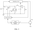
- the synchronous BUCK circuit 100 includes a main switch transistor Q1, an inductor L, a synchronous switch transistor Q2 and an energy-storage capacitor C, where the main switch transistor Q1 has a first terminal connected to a positive electrode of a power supply BAT, a second terminal connected to a first terminal of the inductor L, and a control terminal connected to a control device; the synchronous switch transistor Q2 has a first terminal connected to the second terminal of the main switch transistor Q1 and the first terminal of the inductor L, a second terminal connected to a negative electrode of the power supply, and a control terminal connected to the control device; a second terminal of the inductor L is connected to a positive electrode of the energy-storage capacitor C, and a negative electrode of the energy-storage capacitor C is connected to the negative electrode of the power supply BAT. Both terminals of the energy-storage capacitor C are further connected to a load R L to provide corresponding energy for the load R L .
- the main switch transistor Q1 and the synchronous switch transistor Q2 can be realized by MOS transistors. It can be understood that the synchronous switch transistor Q2 in the above synchronous BUCK circuit uses a rectifier MOS transistor with a low on-resistance to replace a freewheeling diode in the general BUCK circuit so as to reduce a rectification loss of the circuit, which can greatly improve circuit transformation efficiency.
- a body diode in the synchronous switch transistor Q2 shown in FIG. 1 can be used to realize a freewheeling effect of the synchronous BUCK circuit in a discontinuous conduction mode.
- the above synchronous switch transistor Q2 has a parasitic diode (namely, the body diode).
- the body diode in the synchronous switch transistor Q2 can further be replaced by an external independent diode.
- the conventional synchronous BUCK circuit has a sudden switch between a discontinuous conduction mode and a continuous conduction mode when the synchronous switch transistor Q2 is turned on or off, which easily causes a large dynamic impact.
- a current flowing through the inductor in the BUCK circuit gradually decreases to 0 after the main switch transistor Q1 is off for a period of time.
- the current flowing through the inductor does not drop to 0 during each cycle.
- a duty ratio of the main switch transistor Q1 is predicted and controlled at different times, thereby controlling the main switch transistor Q1 and the synchronous switch transistor Q2 according to a predicted value so as to reduce the dynamic impact generated in the circuit.
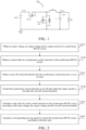
- FIG. 2 a control method for a synchronous BUCK circuit is described in detail below. It can be understood that the synchronous BUCK circuit in FIG. 1 is a basic circuit, and the control method in this embodiment can also be applied to other varied synchronous BUCK circuits.
- Step S110 Obtain an input voltage, an output voltage and an output current of the synchronous BUCK circuit 100.
- a corresponding sampling circuit may be arranged at a corresponding position.
- a sampling unit is arranged at an input terminal of the synchronous BUCK circuit 100 to sample a connected power supply voltage V in .
- the sampling unit may include a divider resistor, an analog-to-digital converter (ADC) and the like.
- ADC analog-to-digital converter
- Another sampling unit may be arranged at an output terminal of the circuit to sample the output current Iout and the output voltage V out .
- a current transformer and the like may be used to sample the output current. It can be understood that a specific structure of the sampling circuit here may be selected according to an actual demand, which is not limited here.
- Step S 120 Obtain a current state of a synchronous switch transistor Q2.
- Step S 130 Obtain a turn-off current threshold when the synchronous switch transistor Q2 is in an on state.
- the on state may also be referred to as a turn-on state
- the off state may also be referred to as a cut-off state or a turn-off state.
- two current thresholds are specified, that is, the turn-off current threshold and a turn-on current threshold.
- the turn-off current threshold is less than the turn-on current threshold.
- the turn-on current threshold and the turn-off current threshold determine a turn-on moment and a turn-off moment of the synchronous switch transistor Q2 respectively.
- the turn-off current threshold is obtained, which is used to, in combination with the output current, determine whether the synchronous switch transistor Q2 needs to be turned off at present. For example, if the present output current is less than the turn-off current threshold, the synchronous switch transistor Q2 is controlled to switch from the present on state to the off state, that is, step S140is performed; otherwise, the present on state is maintained.
- Step S140 Switch the synchronous switch transistor Q2 to the off state when the output current is less than the turn-off current threshold.
- Step S150 Calculate a duty ratio of a main switch transistor Q1 according to the input voltage, the output voltage and the turn-off current threshold.
- the present duty ratio of the main switch transistor Q1 may be calculated according to the following first duty ratio formula.
- Step S 160 Generate a corresponding driving signal according to the duty ratio, to control the synchronous BUCK circuit 100.
- a corresponding PWM driving signal may be generated according to the duty ratio, so as to control the main switch transistor Q1 and the synchronous switch transistor Q2. Because the duty ratio is predicted according to the next working mode of the main switch transistor Q1, directly using the predicted duty ratio to control the main switch transistor Q1 can reduce a current impact generated by the main switch transistor Q1 during the switching between the two working modes of CCM (continuous conduction mode) and DCM (discontinuous conduction mode), thereby improving reliability and output performance of the main switch transistor Q1.
- the synchronous BUCK circuit works in the discontinuous conduction mode, and the main switch transistor Q1 is turned on, the synchronous switch transistor Q2 is tuned off, and in this case, the inductor L stores energy; when the main switch transistor Q1 is turned off, the electric energy stored on the inductor L continues to flow through a body diode or an external diode in the synchronous switch transistor Q2.
- the synchronous BUCK circuit 100 may be controlled by a variety of control technologies, such as voltage mode control, average current control or peak current control. In a practical project, an appropriate control method may be selected according to different demands.
- the synchronous BUCK circuit 100 further includes a loop compensation module.
- a deviation E between a sampled output voltage V out and a preset reference voltage Vref is taken as an input of the loop compensation module.
- the output voltage is adjusted according to an output voltage U used as an adjustment amount for correcting the deviation.
- the loop compensation module may further include a current loop structure. The output voltage U is used as a given value of the current loop, and then a corresponding duty ratio control signal is generated after control and adjustment according to the given value and the output current.
- the loop compensation module is provided with a corresponding discrete domain difference equation.
- the duty ratio of the main switch transistor Q1 or an intermediate quantity that can be used to solve the duty ratio can be calculated according to the discrete domain difference equation.
- U represents the duty ratio or the intermediate quantity for calculating the duty ratio
- n represents a current sample
- n-1 represents a previous sample
- E represents the deviation between the output voltage and the reference voltage
- i and j are integers greater than or equal to 2
- a 1 , A i , B 1 , B 2 and B j represent gain coefficients of corresponding terms respectively. It is understandable that if one of these terms does not exist, the gain coefficient of the corresponding term is 0. That is, an output of the difference equation is not affected by this term.
- control method for a synchronous BUCK circuit further includes the following steps: Step S210. Maintain a current state of the synchronous switch transistor Q2 when the synchronous switch transistor Q2 is in the on state and the output current is greater than or equal to the turn-off current threshold.
- the duty ratio of the main switch transistor Q1 can be calculated according to the above discrete domain difference equation. That is, a conventional duty ratio determining method is used to determine the duty ratio or the intermediate quantity for determining the duty ratio.
- Step S220 Calculate the duty ratio of the main switch transistor Q1 or the intermediate quantity for solving the duty ratio according to the deviation between the output voltage and the reference voltage and the discrete domain difference equation.
- U(n) represents a currently outputted intermediate quantity for calculating the duty ratio and is a control voltage
- U(n-1) represents a previous output, that is, a previous historical intermediate quantity
- E(n) represents a deviation value between the currently sampled output voltage and the reference voltage
- E(n-1) and E(n-2) represent historical deviation values of last two times respectively.
- a corresponding difference equation can directly output a duty ratio of a PWM signal, which is not described here. After the duty ratio is calculated, the two switch transistors in the synchronous BUCK circuit 100 can be controlled accordingly. It can be understood that for different types of loop controllers, such as PI control, PD control or PID control, the expression of the corresponding difference equation also tends to be different.
- Step S230 Generate the corresponding driving signal according to the duty ratio, to control the synchronous BUCK circuit 100, or generate the corresponding driving signal by using the duty ratio after the duty ratio is solved according to the intermediate quantity, to control the synchronous BUCK circuit 100.
- the control device can generate the corresponding PWM driving signal according to the duty ratio so as to drive and control the main switch transistor Q1 and the synchronous switch transistor Q2. If the difference equation outputs the intermediate quantity, such as the above control voltage and the like, the control device can convert the intermediate quantity into the duty ratio of the main switch transistor Q1, and then output the corresponding PWM driving signal.
- the control method for a synchronous BUCK circuit further includes the following steps:
- the turn-on current threshold is obtained, which is used to, in combination with the output current, determine whether the synchronous switch transistor Q2 needs to be turned on at present. For example, if the present output current is greater than the turn-on current threshold, the synchronous switch transistor Q2 is controlled to switch from the present off state to the on state, that is, step S320 is performed; otherwise, the present off state is maintained.
- Step S330 Calculate a duty ratio of the main switch transistor Q1 according to the input voltage and the output voltage.
- the synchronous BUCK circuit After the synchronous switch transistor Q2 is turned on, the synchronous BUCK circuit enters a continuous conduction mode.
- the duty ratio of the main switch transistor Q1 may be calculated according to the following second duty ratio formula.
- Step S340 Generate a corresponding driving signal according to the duty ratio, to control the synchronous BUCK circuit 100.
- a corresponding PWM driving signal may be generated according to the duty ratio so as to control the main switch transistor Q1 and the synchronous switch transistor Q2. Because the duty ratio is predicted according to a next working mode of the main switch transistor Q1, directly using the predicted duty ratio to control the main switch transistor Q1 can reduce a current impact generated by the main switch transistor Q1 during the mode switching, thereby improving reliability and output performance of the main switch transistor Q1.
- control method for a synchronous BUCK circuit further includes the following steps:
- the synchronous switch transistor Q2 is in the off state and the present output current is less than or equal to the turn-on current threshold, the time to turn on the synchronous switch transistor Q2 has not yet arrived. Therefore, the current off state is maintained until the output current is greater than the turn-on current threshold, and then the synchronous switch transistor Q2 is controlled to be turned on.
- Step S430 Generate the corresponding driving signal according to the duty ratio, to control the synchronous BUCK circuit 100; or generate the corresponding driving signal by using the duty ratio after the duty ratio is solved according to the intermediate quantity, to control the synchronous BUCK circuit 100.
- the duty ratio is used to control the synchronous BUCK circuit 100. This step is the same as the above step S230 and the description is not repeated here.
- the method further includes: adjusting a variable of the discrete domain difference equation according to the calculated duty ratio of the main switch transistor Q1, so that an output value of the adjusted discrete domain difference equation is the duty ratio or the intermediate quantity for calculating the duty ratio.
- a value such as a historical output value U(n-1),..., U(n-i) is assigned to an adjustable variable of the discrete domain difference equation according to adjustment of the duty ratio.
- the control method for a synchronous BUCK circuit of this embodiment divides the control of the switch transistor into multiple branches, and uses corresponding duty ratio calculation formulas at different moments to give a predictive control value of the duty ratio, which can avoid a large dynamic impact, thereby affecting reliability and output performance of the switch transistor.
- the synchronous BUCK circuit 100 includes a main switch transistor Q1, an inductor L, a synchronous switch transistor Q2 and an energy-storage capacitor C, where the main switch transistor Q1 has a first terminal connected to a positive electrode of a power supply BAT, a second terminal connected to a first terminal of the inductor L, and a control terminal connected to the control device 200; the synchronous switch transistor Q2 has a first terminal connected to the second terminal of the main switch transistor Q1 and the first terminal of the inductor L, a second terminal connected to a negative electrode of the power supply BAT, and a control terminal connected to the control device 200; a second terminal of the inductor L is connected to a positive electrode of the energy-storage capacitor C, a negative electrode of the energy-storage capacitor C is connected to the negative electrode
- the control device 200 includes an obtaining module 210, a switching module 220, a calculating module 230, and a driving control module 240.
- the obtaining module 210 is configured to obtain an input voltage, an output voltage, and an output current of the synchronous BUCK circuit 100, and obtain a current state of the synchronous switch transistor Q2.
- the obtaining module 210 is further configured to obtain a turn-off current threshold when the synchronous switch transistor Q2 is in an on state.
- the switching module 220 is configured to switch the synchronous switch transistor Q2 to an off state when the output current is less than the turn-off current threshold.
- the calculating module 230 is configured to calculate a duty ratio of the main switch transistor Q1 according to the input voltage, the output voltage and the turn-off current threshold.
- the driving control module 240 is configured to generate a corresponding driving signal according to the duty ratio, to control the synchronous BUCK circuit 100.
- the obtaining module 210 is further configured to obtain a turn-on current threshold when the synchronous switch transistor Q2 is in the off state; the switching module 220 is further configured to switch the synchronous switch transistor Q2 to the on state when the output current is greater than the turn-on current threshold; and the calculating module 230 is further configured to calculate the duty ratio of the main switch transistor Q1 according to the input voltage and the output voltage.
- the synchronous BUCK circuit 100 further includes a loop compensation module, where the loop compensation module is provided with a corresponding discrete domain difference equation so as to determine the duty ratio of the main switch transistor Q1 or an intermediate quantity for solving the duty ratio.
- the switching module 220 is further configured to maintain the current state of the synchronous switch transistor Q2 when the synchronous switch transistor Q2 is in the on state and the output current is greater than or equal to the turn-off current threshold or when the synchronous switch transistor Q2 is in the off state and the output current is less than or equal to the turn-on current threshold.
- the calculating module 230 is further configured to calculate the duty ratio of the main switch transistor Q1 or the intermediate quantity for solving the duty ratio according to a deviation between the output voltage and a reference voltage and the discrete domain difference equation.
- the driving control module 240 is configured to generate the corresponding driving signal according to the duty ratio, to control the synchronous BUCK circuit 100, or generate the corresponding driving signal by using the duty ratio after the duty ratio is solved according to the intermediate quantity, to control the synchronous BUCK circuit 100.
- the embodiment of this application further proposes a synchronous BUCK circuit system.
- the synchronous BUCK circuit system includes: a synchronous BUCK circuit and a control device, where the control device may adopt the control device 200 for a synchronous BUCK circuit in the above embodiment 2.
- the synchronous BUCK circuit 100 includes a main switch transistor Q1, an inductor L, a synchronous switch transistor Q2 and an energy-storage capacitor C, where the main switch transistor Q1 has a first terminal connected to a positive electrode of a power supply BAT, a second terminal connected to a first terminal of the inductor L, and a control terminal connected to the control device 200; the synchronous switch transistor Q2 has a first terminal connected to the second terminal of the main switch transistor Q1 and the first terminal of the inductor L, a second terminal connected to a negative electrode of the power supply BAT, and a control terminal connected to the control device 200; a second terminal of the inductor L is connected to a positive electrode of the energy-storage capacitor C, a negative electrode of the energy-storage capacitor C is connected to the negative electrode of the power supply BAT, and both terminals of the energy-storage capacitor C are further connected to a load in parallel.
- a sampling circuit is mainly configured to sample an input voltage, an output voltage and an output current of the synchronous BUCK circuit 100, and input these sampled electrical signals to the control device 200, so that the control device 200 can control the circuit according to these sampling data.
- a divider resistor can be used to sample at an input end and an output end of the corresponding circuit; for the output current, for example, the output current can be sampled through a current transformer.
- the embodiment of this application further proposes an electronic device.
- the electronic device includes a synchronous BUCK circuit system as in the above embodiment.
- the electronic device may be a power supply device or the like.
- each box in the flowchart or block diagram may represent a module, a program segment or part of a code, where the module, program segment or part of the code contains one or more executable instructions for realizing a specified logical function.
- the functions marked in the boxes may also occur in an order different from that marked in the accompanying drawings.
- each block in the structural diagram and/or flowchart and the combination of blocks in the structural diagram and/or flowchart can be implemented by a dedicated hardware-based system that performs a specified function or action, or by a combination of a dedicated hardware and a computer instruction.
Landscapes
- Engineering & Computer Science (AREA)
- Power Engineering (AREA)
- Dc-Dc Converters (AREA)
- Control Of Eletrric Generators (AREA)
Applications Claiming Priority (2)
| Application Number | Priority Date | Filing Date | Title |
|---|---|---|---|
| CN202110263634.6A CN112636598B (zh) | 2021-03-11 | 2021-03-11 | 同步buck电路的控制方法、装置、系统和电子装置 |
| PCT/CN2021/110805 WO2021254534A2 (zh) | 2021-03-11 | 2021-08-05 | 同步buck电路的控制方法、装置、系统和电子装置 |
Publications (2)
| Publication Number | Publication Date |
|---|---|
| EP4307547A2 true EP4307547A2 (de) | 2024-01-17 |
| EP4307547A4 EP4307547A4 (de) | 2024-08-14 |
Family
ID=75297699
Family Applications (1)
| Application Number | Title | Priority Date | Filing Date |
|---|---|---|---|
| EP21825519.8A Pending EP4307547A4 (de) | 2021-03-11 | 2021-08-05 | Verfahren und vorrichtung zur steuerung einer synchronen abwärtsschaltung, system und elektronische vorrichtung |
Country Status (6)
| Country | Link |
|---|---|
| US (1) | US12374996B2 (de) |
| EP (1) | EP4307547A4 (de) |
| JP (1) | JP7106769B2 (de) |
| KR (1) | KR102572644B1 (de) |
| CN (1) | CN112636598B (de) |
| WO (1) | WO2021254534A2 (de) |
Families Citing this family (4)
| Publication number | Priority date | Publication date | Assignee | Title |
|---|---|---|---|---|
| CN112636598B (zh) * | 2021-03-11 | 2021-05-25 | 深圳市正浩创新科技有限公司 | 同步buck电路的控制方法、装置、系统和电子装置 |
| CN116094326A (zh) * | 2023-01-13 | 2023-05-09 | 唐山松下产业机器有限公司 | 基于同步buck电路的防止泵生电压逆流的控制方法及装置 |
| CN116345906A (zh) * | 2023-03-28 | 2023-06-27 | 苏州海鹏科技有限公司 | 基于双向直流变换器电路的控制方法 |
| CN120433582A (zh) * | 2024-02-02 | 2025-08-05 | 浙江维思无线网络技术有限公司 | 一种buck电路pwm波形生成方法及装置 |
Family Cites Families (24)
| Publication number | Priority date | Publication date | Assignee | Title |
|---|---|---|---|---|
| TW595077B (en) * | 2002-04-03 | 2004-06-21 | Int Rectifier Corp | Synchronous buck converter improvements |
| US7743266B2 (en) * | 2002-12-21 | 2010-06-22 | Power-One, Inc. | Method and system for optimizing filter compensation coefficients for a digital power control system |
| US7436162B2 (en) * | 2005-04-15 | 2008-10-14 | International Rectifier Corporation | Buck converter having improved transient response to load step down |
| US7911816B2 (en) * | 2006-09-13 | 2011-03-22 | Hypertherm, Inc. | Linear, inductance based control of regulated electrical properties in a switch mode power supply of a thermal processing system |
| US7535210B2 (en) * | 2006-10-18 | 2009-05-19 | Texas Instruments Incorporated | Predictive duty ratio generating circuit and method for synchronous boost converters operating in PFM mode |
| US7800352B2 (en) * | 2007-05-16 | 2010-09-21 | Intersil Americas Inc. | Controller having comp node voltage shift cancellation for improved discontinuous conduction mode (DCM) regulator performance and related methods |
| US8686698B2 (en) * | 2008-04-16 | 2014-04-01 | Enpirion, Inc. | Power converter with controller operable in selected modes of operation |
| US8742744B2 (en) * | 2009-01-13 | 2014-06-03 | University Of Alabama | Sensor-less operation and detection of CCM and DCM operation modes in synchronous switching power converters |
| US9124177B2 (en) * | 2010-08-10 | 2015-09-01 | Texas Instruments Incorporated | Systems and methods of smooth light load operation in a DC/DC converter |
| CN102202449B (zh) * | 2011-06-30 | 2014-07-02 | 杭州士兰微电子股份有限公司 | Led驱动控制电路及方法 |
| US8638080B2 (en) * | 2011-09-14 | 2014-01-28 | Texas Instruments Incorporated | Circuits and methods for controlling PWM input of driver circuit |
| US8791647B2 (en) * | 2011-12-28 | 2014-07-29 | Dialog Semiconductor Inc. | Predictive control of power converter for LED driver |
| US9444332B2 (en) * | 2013-10-07 | 2016-09-13 | Infineon Technologies Austria Ag | System and method for controlling a power supply during discontinuous conduction mode |
| CN104362851B (zh) * | 2014-10-15 | 2017-04-26 | 西安交通大学 | 一种dc‑dc转换器控制系统 |
| JP6323389B2 (ja) * | 2015-04-27 | 2018-05-16 | 株式会社オートネットワーク技術研究所 | Dc/dcコンバータ |
| US10090663B2 (en) * | 2016-01-11 | 2018-10-02 | Semiconductor Components Industries, Llc | Over-current protection circuit and method for voltage regulators |
| US9806617B1 (en) * | 2016-09-09 | 2017-10-31 | Dialog Semiconductor (Uk) Limited | Switch mode power converter with overshoot and undershoot transient control circuits |
| JP6289574B1 (ja) * | 2016-09-30 | 2018-03-07 | 三菱電機株式会社 | 直流電力変換器 |
| CN111697828A (zh) * | 2016-10-09 | 2020-09-22 | 昂宝电子(上海)有限公司 | Buck变换器及其控制方法 |
| US10525841B2 (en) * | 2016-10-12 | 2020-01-07 | Ford Global Technologies, Llc | Gate driver with short circuit protection |
| US10715039B1 (en) * | 2018-03-07 | 2020-07-14 | Cirrus Logic, Inc. | Peak current controlled switch mode power supply with embedded adaptive pulse frequency modulation control |
| DE102019200697A1 (de) * | 2019-01-21 | 2020-07-23 | Dialog Semiconductor (Uk) Limited | Steuerung der Pulsfrequenzmodulation eines Leistungswandlers |
| CN110138209B (zh) * | 2019-05-13 | 2021-08-06 | 矽力杰半导体技术(杭州)有限公司 | 开关电源的模式切换电路和模式切换方法 |
| CN112636598B (zh) * | 2021-03-11 | 2021-05-25 | 深圳市正浩创新科技有限公司 | 同步buck电路的控制方法、装置、系统和电子装置 |
-
2021
- 2021-03-11 CN CN202110263634.6A patent/CN112636598B/zh active Active
- 2021-08-05 KR KR1020217036453A patent/KR102572644B1/ko active Active
- 2021-08-05 JP JP2021562301A patent/JP7106769B2/ja active Active
- 2021-08-05 WO PCT/CN2021/110805 patent/WO2021254534A2/zh not_active Ceased
- 2021-08-05 EP EP21825519.8A patent/EP4307547A4/de active Pending
-
2022
- 2022-09-21 US US17/949,838 patent/US12374996B2/en active Active
Also Published As
| Publication number | Publication date |
|---|---|
| JP2022532301A (ja) | 2022-07-14 |
| JP7106769B2 (ja) | 2022-07-26 |
| KR102572644B1 (ko) | 2023-08-29 |
| US12374996B2 (en) | 2025-07-29 |
| WO2021254534A2 (zh) | 2021-12-23 |
| KR20220128264A (ko) | 2022-09-20 |
| EP4307547A4 (de) | 2024-08-14 |
| CN112636598A (zh) | 2021-04-09 |
| US20230011390A1 (en) | 2023-01-12 |
| WO2021254534A3 (zh) | 2022-02-10 |
| CN112636598B (zh) | 2021-05-25 |
Similar Documents
| Publication | Publication Date | Title |
|---|---|---|
| EP4307547A2 (de) | Verfahren und vorrichtung zur steuerung einer synchronen abwärtsschaltung, system und elektronische vorrichtung | |
| US11323030B2 (en) | Control method for DC/DC converter and DC/DC converter for achieving continuous voltage gain | |
| CN112688538B (zh) | 准恒定导通时间控制电路及其开关变换器和方法 | |
| CN101728954B (zh) | 用于dc-dc变流器的控制电路及其方法 | |
| CN106208692B (zh) | 开关电路的控制方法、控制电路及开关电路装置 | |
| US9343986B2 (en) | Power converter with current feedback loop | |
| US20120294052A1 (en) | Monotonic pre-bias start-up of a dc-dc converter | |
| WO2009139249A1 (en) | Current-mode control switching regulator and operations control method thereof | |
| US20170237332A1 (en) | Power Converter with Zero-Voltage Switching Control | |
| US11121630B2 (en) | In-vehicle DC-DC converter | |
| US20220158536A1 (en) | Soft-start for resonant converters | |
| CN105048811A (zh) | Dc-dc变换器的导通时间校正定频跨周期控制器及方法 | |
| CN103633831B (zh) | 控制电路、时间计算单元及控制电路操作方法 | |
| CN106712528A (zh) | Llc谐振变换器驱动脉冲个数调制方法及单元 | |
| US20230058021A1 (en) | Circuits and method for reducing light load power dissipation of a voltage converter | |
| CN104092359A (zh) | 一种用于多模式数字开关电源的控制环路系统 | |
| CN203135724U (zh) | 开关变换器及其斜坡补偿电路 | |
| CN103595239B (zh) | 功率因数校正电路及其控制方法 | |
| CN206041805U (zh) | 开关电路的控制电路及开关电路装置 | |
| Vasconselos et al. | A hybrid digital control method for synchronous buck converters using multisampled linear PID and V 2 constant on-time controllers | |
| KR102772287B1 (ko) | 부하량 기반 dc-dc 컨버터 | |
| Bai et al. | Switching Sequence Based Energy Prediction Controller Design for Bidirectional DC-DC Converters | |
| JP2019075855A (ja) | スイッチング素子の制御回路、電源装置、スイッチング素子の制御方法及びコンピュータプログラム | |
| CN118449374A (zh) | 一种直流变换器及直流变换器的控制方法 | |
| CN121566926A (zh) | 一种整流电路的控制方法、电源控制电路 |
Legal Events
| Date | Code | Title | Description |
|---|---|---|---|
| STAA | Information on the status of an ep patent application or granted ep patent |
Free format text: STATUS: THE INTERNATIONAL PUBLICATION HAS BEEN MADE |
|
| PUAI | Public reference made under article 153(3) epc to a published international application that has entered the european phase |
Free format text: ORIGINAL CODE: 0009012 |
|
| STAA | Information on the status of an ep patent application or granted ep patent |
Free format text: STATUS: REQUEST FOR EXAMINATION WAS MADE |
|
| 17P | Request for examination filed |
Effective date: 20231010 |
|
| AK | Designated contracting states |
Kind code of ref document: A2 Designated state(s): AL AT BE BG CH CY CZ DE DK EE ES FI FR GB GR HR HU IE IS IT LI LT LU LV MC MK MT NL NO PL PT RO RS SE SI SK SM TR |
|
| DAV | Request for validation of the european patent (deleted) | ||
| DAX | Request for extension of the european patent (deleted) | ||
| A4 | Supplementary search report drawn up and despatched |
Effective date: 20240716 |
|
| RIC1 | Information provided on ipc code assigned before grant |
Ipc: H02M 3/158 20060101AFI20240710BHEP |
|
| STAA | Information on the status of an ep patent application or granted ep patent |
Free format text: STATUS: EXAMINATION IS IN PROGRESS |
|
| 17Q | First examination report despatched |
Effective date: 20250214 |