EP4301697B1 - Eine vorrichtung zur aktiven modifikation der wärmestrahlung - Google Patents
Eine vorrichtung zur aktiven modifikation der wärmestrahlung Download PDFInfo
- Publication number
- EP4301697B1 EP4301697B1 EP22710092.2A EP22710092A EP4301697B1 EP 4301697 B1 EP4301697 B1 EP 4301697B1 EP 22710092 A EP22710092 A EP 22710092A EP 4301697 B1 EP4301697 B1 EP 4301697B1
- Authority
- EP
- European Patent Office
- Prior art keywords
- carbon nanotubes
- polymeric
- electrodes
- ionic liquid
- membranes
- Prior art date
- Legal status (The legal status is an assumption and is not a legal conclusion. Google has not performed a legal analysis and makes no representation as to the accuracy of the status listed.)
- Active
Links
Images


Classifications
-
- F—MECHANICAL ENGINEERING; LIGHTING; HEATING; WEAPONS; BLASTING
- F41—WEAPONS
- F41H—ARMOUR; ARMOURED TURRETS; ARMOURED OR ARMED VEHICLES; MEANS OF ATTACK OR DEFENCE, e.g. CAMOUFLAGE, IN GENERAL
- F41H3/00—Camouflage, i.e. means or methods for concealment or disguise
- F41H3/02—Flexible, e.g. fabric covers, e.g. screens, nets characterised by their material or structure
-
- C—CHEMISTRY; METALLURGY
- C01—INORGANIC CHEMISTRY
- C01B—NON-METALLIC ELEMENTS; COMPOUNDS THEREOF; METALLOIDS OR COMPOUNDS THEREOF NOT COVERED BY SUBCLASS C01C
- C01B32/00—Carbon; Compounds thereof
- C01B32/15—Nano-sized carbon materials
- C01B32/158—Carbon nanotubes
-
- C—CHEMISTRY; METALLURGY
- C01—INORGANIC CHEMISTRY
- C01B—NON-METALLIC ELEMENTS; COMPOUNDS THEREOF; METALLOIDS OR COMPOUNDS THEREOF NOT COVERED BY SUBCLASS C01C
- C01B32/00—Carbon; Compounds thereof
- C01B32/15—Nano-sized carbon materials
- C01B32/158—Carbon nanotubes
- C01B32/159—Carbon nanotubes single-walled
-
- C—CHEMISTRY; METALLURGY
- C01—INORGANIC CHEMISTRY
- C01B—NON-METALLIC ELEMENTS; COMPOUNDS THEREOF; METALLOIDS OR COMPOUNDS THEREOF NOT COVERED BY SUBCLASS C01C
- C01B2202/00—Structure or properties of carbon nanotubes
- C01B2202/02—Single-walled nanotubes
-
- C—CHEMISTRY; METALLURGY
- C01—INORGANIC CHEMISTRY
- C01B—NON-METALLIC ELEMENTS; COMPOUNDS THEREOF; METALLOIDS OR COMPOUNDS THEREOF NOT COVERED BY SUBCLASS C01C
- C01B2202/00—Structure or properties of carbon nanotubes
- C01B2202/20—Nanotubes characterized by their properties
- C01B2202/22—Electronic properties
-
- C—CHEMISTRY; METALLURGY
- C01—INORGANIC CHEMISTRY
- C01B—NON-METALLIC ELEMENTS; COMPOUNDS THEREOF; METALLOIDS OR COMPOUNDS THEREOF NOT COVERED BY SUBCLASS C01C
- C01B2202/00—Structure or properties of carbon nanotubes
- C01B2202/20—Nanotubes characterized by their properties
- C01B2202/34—Length
-
- C—CHEMISTRY; METALLURGY
- C01—INORGANIC CHEMISTRY
- C01B—NON-METALLIC ELEMENTS; COMPOUNDS THEREOF; METALLOIDS OR COMPOUNDS THEREOF NOT COVERED BY SUBCLASS C01C
- C01B2202/00—Structure or properties of carbon nanotubes
- C01B2202/20—Nanotubes characterized by their properties
- C01B2202/36—Diameter
-
- C—CHEMISTRY; METALLURGY
- C01—INORGANIC CHEMISTRY
- C01P—INDEXING SCHEME RELATING TO STRUCTURAL AND PHYSICAL ASPECTS OF SOLID INORGANIC COMPOUNDS
- C01P2004/00—Particle morphology
- C01P2004/01—Particle morphology depicted by an image
- C01P2004/03—Particle morphology depicted by an image obtained by SEM
Definitions
- This present invention relates to devices with low thermal emissivity containing carbon nanomaterials, methods of making such devices and applications of the devices.
- thermal emissivities from surfaces is important for a range of industrial applications which require the reduction of a thermal signature to assist in the overall heat efficiency and heat loss.
- thermal regulation of buildings it is desirable to reduce and control emissitivites commensurate with solar radiation profiles to reduce the energy costs of heating and cooling.
- materials with tunable infra-red properties, such as transparency and/or emissivity may be useful in thermal windows and emissive temperature control.
- Carbon nanotubes are nanosized tubes constructed from rolled sheets of graphite.
- the tubes typically have a diameter in the range of 1 to 50 nanometres, but can have lengths in the micrometre range.
- Carbon nanotubes can be either single-walled (i.e. formed from a single rolled sheet of graphene) or multi-walled (i.e. formed from a plurality of concentric rolled sheets of graphene).
- Carbon nanotubes have attracted great interest due to their physical properties - namely their high tensile strength and high electrical conductivity.
- 2D materials are known to have many interesting and potentially useful properties, which differ from the properties of the corresponding bulk 3D material.
- graphene is highly conductive and has applications in electrode structures as well as in conductive composites.
- the interesting functional properties of many materials are often only observed when the materials are in their mono- or few-layer (i.e. 2D) forms.
- 2D mono- or few-layer
- the strong interlayer dispersion forces must be overcome in order to exfoliate bulk three-dimensional (3D) materials to form the corresponding 2D materials. Liquid phase exfoliation and dispersion using high shear mixing is an accessible route towards producing formulated inks containing 2D materials which find uses in many industrial applications.
- Liyuan et al., Nanomaterials (2019), 8, 1096 describes a flexible graphene-based thermal camouflage device comprising a layer of graphene, a layer of a porous polyethylene membrane soaked with an ionic liquid, and a layer of a copper electrode to form a planar capacitor.
- thermal camouflage preferably those with improved properties, including improved scalability (for example, areal scalability).
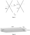
- a thermally adaptive camouflage device comprising nanoparticulate graphite/graphene and/or carbon nanotubes can use the principle of Pauli Blocking to modify the band structure of graphene to block state transitions (see Figure 1 ).
- the band structure of graphene can be simplified and represented as a Dirac cone in which energy (E) is linear with momentum (k).
- E energy
- k momentum
- the Fermi Level the state below which all states are occupied at absolute zero, rests close to the point of the cones.
- An incident photon would then cause excitation of an electron into an empty state causing an absorption event ( Figure 1 - left).
- the Fermi level can be raised causing the occupancy of more states. If the same photon then interacts with the modified graphene the electron cannot be excited due to there being no available unoccupied state ( Figure 1 - right).
- the fabrication method For large area devices, it is preferable for the fabrication method to be solution-based (rather than, for example, based around the transfer of ultra-thin film CVD deposited graphene).
- the construction of the electrolytic capacitor device also requires elements of a thin porous membrane separator and a liquid ionic electrolyte to be developed such that fast switching times and large observable differences can be obtained.
- Nanocarbon materials also exhibit a large surface area to volume ratio which assists the accumulation of charge on local surfaces. The operating range and switching times of these devices therefore are also driven by the physical properties of the electrolyte and the diffusivity into the internal structure of the electrode.
- the electrode film's internal resistive losses are minimised as far as possible by the use of conductive carbon nanomaterials (for example carbon nanotubes and/or graphite nanoplatelets).
- the invention provides a device for active modification of thermal radiation, the device comprising:
- the one or more electrodes may comprise additional carbon nanomaterials, in addition to carbon nanotubes.
- the electrodes may comprise carbon nanotubes together with graphite nanoplatelets (also referred to as few-layer graphene).
- the electrodes are deposited onto the polymeric membrane(s) such that the electrodes are in contact with polymeric membrane(s) to allow ionic/electron transport from the polymeric membrane(s) to the electrodes. These polymeric membrane(s) serve as separators to prevent electrical shorting between the electrodes.
- a potential difference is applied to the pair of electrodes, the occupation of electrons in the Fermi level of the electrodes can be adjusted and therefore the thermal emissivity of the device can be altered.
- the devices can be used for the active modification of thermal radiation. This may include modulating the transparency and/or reflectance of the device or the emissivity of the device.
- Another example of this is is the reduction of heat loss within glazing products.
- Glass exhibits a high emmisivity and thus radiates heat readily. By lowering the outer emmisivity relative to the environment, heat loss can be reduced.
- the devices of the invention are therefore able to be either integrated within glazing laminates or affixed as an outer laminate.
- the thermal radiation detected by the detector is reduced.
- the devices of the invention can therefore effectively block thermal radiation from heat sources and therefore can act as thermal camouflaging devices.
- the devices for active modification of thermal radiation can therefore also be considered to be devices for camouflaging/concealing/masking/obscuring/suppressing thermal radiation.
- the invention also provides a method of actively modifying (e.g. camouflaging/concealing) thermal radiation from an object, the method comprising placing a device as described herein between the object and a thermal radiation detector.
- the method may include covering or surrounding the object with a device as described herein.
- a further example of this is for the protection of sensitive infra-red detector devices which are used for astronomical observation.
- the devices can be formed by depositing (e.g. printing or spraying) an ink containing the carbon nanomaterials onto one or onto a pair of polymeric membranes.
- the polymeric membranes(s) are typically infused with the ionic liquid.
- the polymeric membrane may be formed as a porous membrane and then, following its formation, the ionic liquid may be applied to (e.g. soaked into) the porous membrane such that it infiltrates into the pores therein.
- the polymeric membrane(s) can be infused with the ionic liquid before or after the electrodes are deposited onto the membrane.
- the polymeric membrane may be co-cast with the ionic liquid to form the infused polymeric membrane.
- the invention also provides a method of making a device as described herein, the method comprising:
- the polymeric membranes comprising the ionic liquid may be formed before the liquid composition comprising carbon nanomaterials is printed onto the polymeric membrane. Accordingly, the invention also provides a method of making a device as described herein, the method comprising:
- Step (a) may comprise impregnating the polymeric permeable membranes with the ionic liquid or co-casting the membranes from a polymer and the ionic liquid.
- the invention also provides a method of making a device as described herein, the method comprising:
- the methods above may also comprise the steps of securing the first and second polymeric membranes to a substrate and/or applying a protective encapsulation layer to the polymeric membranes.
- the invention additionally provides devices obtained according to the methods described herein.
- carbon nanomaterials or “nanocarbon” as used herein refers to nanomaterials (i.e. materials having an average size from 1nm to 100nm in at least one dimension) that comprise or consist of carbon.
- the carbon nanomaterials comprise at least 90% or more by weight, preferably at least 95% or more by weight, for example 99% or more by weight of carbon.
- the term includes materials such as graphene, graphite nanoplatelets, single-walled carbon nanotubes, multi-walled carbon nanotubes, crystalline diamond, and diamond-like carbon (see the following ISO standard: ISO/TS 80004-3:2020).
- the electrodes comprise carbon nanotubes (preferably single-walled carbon nanotubes).
- the electrodes may also comprise graphite nanoplatelets.
- the carbon nanotubes may be single-walled carbon nanotubes or multi-walled carbon nanotubes, but preferably comprise or consist of single-walled carbon nanotubes.
- the carbon nanotubes may be metallic carbon nanotubes or semiconductor carbon nanotubes.
- the carbon nanotubes typically have an outer mean diameter of from 1nm to 5nm, preferably from 1nm to 2nm (as determined by transmission electron microscopy) and may have a length of greater than 3 ⁇ m, typically greater than 5 ⁇ m, for example greater than 10 ⁇ m or greater than 15 ⁇ m. Whereas the nanoplatelets described below are micron-sized in two dimensions, carbon nanotubes are only micron-sized in a single dimension (i.e. along their length).
- graphite nanoplatelets refers to nanoparticles of graphite which consist of small stacks of graphene.
- graphite nanoplatelets refers to nanoplatelets having on average 20 or fewer layers, typically 15 layers or fewer, preferably 10 or fewer layers. Layer numbers can be determined by UV-vis spectroscopy (see C. Backes et al., 'Spectroscopic metrics allow in-situ measurement of mean size and thickness of liquid-exfoliated graphene nanosheets', Nanoscale, 2016, doi: 10.1039/C5NR08047A ).
- the nanoplatelets typically have an average thickness of less than 30nm, for example less than 20nm.
- the term “thickness” as used herein refers to the dimension of the nanoplatelets along the axis of stacking of the layers within the nanoplatelets.
- the terms “length” and “width” refer to the longer and shorter dimensions of the nanoplatelets along perpendicular axes in the plane of the sheets of the layered materials respectively (see Figure 2 ).
- the nanoplatelets typically have an average length and/or width of 30nm or greater, preferably 50nm or greater or 100nm or greater.
- the nanoplatelets typically have an average length and/or width of 10 ⁇ m or less, typically 3.0 ⁇ m or less, for example 2.0 ⁇ m or less, typically 1.5 ⁇ m or less, preferably 1 ⁇ m or less, for example 800nm or less.
- graphite nanoplatelets have larger lateral dimensions that are greater than 1 ⁇ m and less than 50 ⁇ m.
- the number vs size distributions of these materials may be broad or narrow depending on the exfoliation technique employed and/or any subsequent size selection process.
- the dimensions of the nanoplatelets can be measured using scanning or transmission electron microscopy.
- the nanoplatelets are typically only micron-sized in up to two dimensions (i.e. their length and width, with their thickness being significantly less than 1 ⁇ m, for example less than 100nm). These dimensions are preferably measured by transmission electron microscopy.
- the graphite nanoplatelets are typically present in the electrodes in an amount of from 25% (w/w), preferably from 30% (w/w), for example from 35% (w/w) and up to 50% (w/w), preferably up to 45% (w/w), for example up to 40% (w/w).
- the carbon nanotubes may be present in the electrodes described herein in a weight ratio relative to the amount of graphite nanoplatelets of greater than 0.15:1 (carbon nanotubes:graphite nanoplatelets), preferably greater than 0.2:1 and in a ratio of up to 1:1, suitably up to 0.7:1, preferably up to 0.6:1.
- the carbon nanotubes are typically present in the electrodes in a weight ratio relative to the amount of graphite nanoplatelets of from 0.15:1 to 0.6:1 (carbon nanotubes:graphite nanoplatelets), preferably in a ratio of from 0.4:1 to 0.5:1.
- the quantity of carbon nanotubes in the electrodes may be defined relative to the weight of the total composition.
- the carbon nanotubes are typically present in the electrodes composition in an amount of from 5% (w/w), preferably from 10% (w/w), for example from 15% (w/w) and up to 30% (w/w), preferably up to 25% (w/w), for example up to 20% (w/w).
- the carbon nanotubes may be present in the electrodes in an amount of 50% or greater, preferably 75% or greater by weight, such as 90% or greater by weight, for example 95% or greater by weight.
- the electrodes typically have a thickness of from 10nm to 750nm, typically from 20nm to 500nm, for example from 50nm to 250nm.
- the electrodes are typically deposited onto the polymeric membrane from a liquid composition (or "ink").
- a liquid composition or "ink”
- liquid compositions comprising the carbon nanomaterials and a solvent (and optionally other thickening agents, binders and other additivities described below) can be sprayed or printed onto the polymeric membrane.
- the solvent may be an aqueous or non-aqueous solvent.
- the solvent preferably is or comprises water (necessary for hydrogel formation).
- the solvent may be a dipolar aprotic solvent.
- dipolar aprotic solvents include cyclopentanone, cyclohexanone, N-methylpyrrolidone (NMP), dimethylformamide (DMF), dimethylsulphoxide (DMSO), dimethylacetamide (DMAc), sulpholane, dihydrolevoglucosenone (Cyrene) and lactones, such as gamma-valerolactone.
- gamma-valerolactone When gamma-valerolactone is present, it may be present in the liquid compositions in amount of from 1% to 10% (w/w), for example up to 5% (w/w) or from 5% (w/w) to 10% (w/w), preferably from 6% to 10% (w/w).
- the liquid compositions may also include a thickening agent (which may also act as gelification agents) to increase the viscosity of the compositions.
- a thickening agent which may also act as gelification agents to increase the viscosity of the compositions.
- the increased viscosity ensures that the compositions are suitable for printing and also reduces tendency of the carbon nanomaterials to flocculate from suspension.
- the thickening agent is preferably a hydrogel-forming thickening agent.
- the formation of a hydrogel matrix containing carbon nanotubes and additional carbon nanomaterials (for example, graphite nanoplatelets) results in a highly electrically conductive ink.
- the hydrogel-forming thickening agents are generally hydrophilic polymer chains which form a colloidal gel through hydrogen-bonding in water.
- Suitable thickening agents include:
- the thickening agent is a cellulose derivative, such as carboxymethyl cellulose.
- cellulose derivate refers to chemical derivatives of cellulose formed by functionalisation of some or all of the hydroxyl groups present in cellulose (for example via etherification or esterification reactions). Derivatives can be formed by incorporation of one or more or all of carboxy, hydroxy, methyl, ethyl and/or propyl groups. Examples of cellulose derivatives include hydroxypropyl methylcellulose, hydroxypropyl cellulose, methyl ethyl cellulose, methyl cellulose and carboxymethylcellulose or a combination thereof, as well as cellulose itself.
- CMC is available in several forms (e.g. varying by degree of substitution and function) and can be crosslinked with several chemical agents either covalently or through hydrogen bonding networks with other agents to impart new properties which can be tailored according to requirements ( Gels 2018, 4, 54; doi: 1 0.3390/gels4020054 ).
- the total concentration of the thickening agents may be in the range of 0.5% to 2% by weight of the total liquid composition (including the solvent), for example from 1% to 1.75% by weight of the total liquid composition.
- the thickening agent increases the viscosity of the composition and it is envisaged that it also enables the carbon nanotubes to form a pre-ordered supramolecular network, which increases the conductivity of electrodes printed from the composition.
- the viscosity of the composition is important to ensure that it can be printed to form a film.
- the composition should be viscous enough to prevent flocculation of the carbon nanomaterials within the composition.
- the precise viscosity will of course depend on the application of the composition (and the resulting film).
- the thickening agent also ensures that the inks have a viscosity suitable for printing, e.g. screen printing.
- the inks suitable for screen-printing are typically thixotropic and therefore their viscosity is dependent on shear rate.
- the liquid compositions may have a viscosity of from 100 to 1000 Pa.s at a shear rate of 0.1/s and/or may have a viscosity of from 1 to 10 at a shear rate of 100/s.
- the liquid compositions may also include one or more surfactants.
- the surfactants are typically non-ionic surfactants.
- suitable non-ionic surfactants include polyethylene oxide-based (PEO) surfactants (e.g. Triton X-100), polypropylene oxide-based (PPO) surfactants, cyclodextrins and polyvinyl pyrrolidone (PVP) surfactants.
- PEO polyethylene oxide-based
- PPO polypropylene oxide-based
- PVP polyvinyl pyrrolidone
- ionic surfactants such as sulphate-based surfactants (such as sodium dodecyl sulphate) may also be used.
- the total concentration of the surfactants may be in the range of 0.01 % to 1 % or 0.01 % to 0.1% by weight of the total composition (including the solvent), for example from 0.02% to 0.05% by weight of the total composition.
- compositions may also comprise one or more solvents and or adhesives in order to improve adhesion of the dried film (formed by printing the ink) to a substrate.
- adhesives will of course be dependent on the substrate.
- compositions may also comprise one or more humectants to aid the printability of the inks within industrial processes.
- humectants to aid the printability of the inks within industrial processes.
- the addition of urea, glycerin, or glycols such as polypropylene glycol slows the ink drying process such that constant and repeatable printing can be obtained.
- films formed with binders containing mono-valent ions such as sodium carboxymethyl cellulose
- films formed with binders containing mono-valent ions may be treated with aqueous solutions of bi, tri or tetra valent ionic salts such as Calcium (II) Chloride or Iron (III) Sulphate to form ionically-cross-linked insoluble films by a process of ion exchange.
- bi, tri or tetra valent ionic salts such as Calcium (II) Chloride or Iron (III) Sulphate
- the carbon nanomaterial-containing liquid compositions are deposited on a polymeric membrane as electrodes to form the device of the invention.
- the device comprises a pair of electrodes.
- the electrodes may both comprise carbon nanotubes (and optionally additional carbon nanomaterials).
- the electrodes may be formed from different materials.
- a first electrode may comprise carbon nanotubes and a second electrode may be a metallic electrode.
- the electrode adjacent the substrate is a non-carbon nanomaterial containing electrode.
- the device preferably comprises a pair of electrodes comprising carbon nanotubes (and optionally further carbon nanomaterials, such as graphite nanoplatelets).
- devices of the invention may comprise a first carbon-containing electrode and a second electrode, which has a different composition to the first electrode.
- the second electrode may be a metallic electrode, such as a gold, silver or copper electrode.
- the polymeric permeable membrane is a dielectric material and is therefore electrically insulating.
- the polymeric membrane is also capable of holding an ionic liquid (in a similar manner to a capacitor or battery device).
- the polymeric membrane may comprise polyethylene, polypropylene, polyvinylidene fluoride (PVDF), polyimide, cellulose, a cellulose derivative, or a mixture thereof.
- the polymeric membrane is a polyethylene (PE) membrane, a polypropylene (PP) membrane or a PE/PP membrane.
- the ionic liquid is preferably a room temperature ionic liquid.
- Room temperature ionic liquids are a class of liquids with a low melting point that allow conductivity due to their ionic nature.
- the ionic liquid preferably has an electrochemical window of (plus/minus) 4V or greater, for example 4.5V or greater.
- the ionic liquid may be introduced or infused into the polymeric membrane either during or after its production.
- the polymeric membrane is infused with the ionic liquid by first forming a porous polymeric membrane and then applying (e.g. soaking) the ionic liquid into the membrane.
- the ionic liquid infused membrane comprises a solid co-cast film of a suitable polymer with an ionic liquid commonly know as a solid polymer electrolyte.
- a dielectric polymer and the ionic liquid are dissolved in a appropriate solvent, in which they are both soluble (for example polar, aprotic solvents, such as acetone, DMF or NMP) and then the solvent is removed to form the polymeric layer infused with the ionic liquid.
- the polymeric membrane When the polymeric membrane is co-cast from the polymer and ionic liquid, it may be cast on top of a previously coated layer of the electrode comprising carbon nanotubes. This approach has several advantges. Firstly, this reduces the seepable liquids which could leak from the device. Secondly, the method of device construction can be made simpler by virtue of a multistep coating and encapsulation process. In addition, mechanically, the device is less prone to electrical breakdown through localised stress induced damage.
- the devices described herein may be exposed to the environment in use, they should be able to be operated sufficiently in ambient conditions.
- Water present in the air is one possible source of detrimental effects due to the low potential window of water to electrolysis (1.23V) as well as material interaction considerations.
- the ionic liquids are preferably hydrophobic ionic liquids.
- ionic liquids for use in the devices described herein are diethylmethyl(2-methoxyethyl)ammonium salts, including diethylmethyl(2-methoxyethyl)ammonium bis(trifluoromethylsulfonyl)imide ([DEME][TFSI]) and [DEME][BF 4 ], as well as 1-ethyl-3-methylimidazlium salts, e.g. EMI-BF 4 and [EMI][TFSI].
- the ionic liquid may be a lithium-based ionic liquid (i.e. an ionic liquid wherein the cation is Li + ), for example LiClO 4 or Li[TFSI].
- the polymeric permeable membrane typically has a thickness of from 100nm to 100 ⁇ m, for example from 1 ⁇ m to 50 ⁇ m, for example from 1 ⁇ m to 30 ⁇ m.
- the device may have a laminar structure wherein a sheet (or sheets) of the polymeric membrane is/are sandwiched between the electrode films and the combination of the polymeric membrane(s) and electrode(s) are mounted on a substrate.
- the substrate may be comprised of a rigid or flexible planar material which may comprise a continuous organic polymer, silicate based glass or a conductive metallic sheet.
- the substrate may also be metalised by various means to facilitate an efficient electrode.
- This substrate may be coated with nanocarbon material to aid industrial production.
- Devices may be protected from ambient moisture ingress using a top encapsulation substrate atop the device.
- This barrier layer may comprise one or more layers of continuous material.
- Such encapsulation layers may be formed from suitable barrier materials with low absorption characteristics in the IR spectrum, such as poly(ethylene), flexible glass, quartz, sapphire, alkali metal halides, polycarbonates and poly(methyl)methacrylate.
- the assembled laminar structure of the polymeric membrane(s) and electrode(s) typically has a thickness of less than 1cm, for example less than 500 microns, or less than 100 microns, or less than 50 microns.
- the assembled laminar structure typically has a thickness of greater than 5 microns, such as greater than 10 microns.
- the layers of the laminar structure typically have a surface area of greater than 20cm 2 , typically greater than 100cm 2 .
- the device is connectable or connected to a power source, for example a battery. More specifically, a power source is connectable or connected to the electrodes of the device. The potential difference applied across the electrodes by the power source alters the Fermi level of the carbon nanomaterials (e.g. the graphite nanoplatelets) within the electrodes to provide a thermal camouflaging effect.
- a power source for example a battery. More specifically, a power source is connectable or connected to the electrodes of the device.
- the potential difference applied across the electrodes by the power source alters the Fermi level of the carbon nanomaterials (e.g. the graphite nanoplatelets) within the electrodes to provide a thermal camouflaging effect.
- the device may also comprise one or more switches or control circuitry for controlling the supply of power to the electrodes or varying the potential difference supplied by the power source to the electrodes of the device.
- the device and the layers within the device may have the structure or properties of the device or layers described above in connection with devices for active modification of thermal radiation.
- the invention provides a device for active modification of (e.g. camouflaging) thermal radiation, the device comprising:
- the invention provides a device for active modification of (e.g. camouflaging) thermal radiation, the device comprising:
- the invention provides a method of making a device as described herein, the method comprising:
- the polymeric membranes comprising the ionic liquid may be formed before the liquid composition comprising carbon nanomaterials is printed onto the polymeric membrane. Accordingly, the invention also provides a method of making a device as described herein, the method comprising:
- the devices of the invention can be prepared by subsequent deposition of layers onto the substrate. Accordingly, in a further aspect, the invention provides a method of making a device as described herein, the method comprising:
- the liquid compositions in steps b), c) and d) typically further comprise a solvent (as described above). Accordingly, the method may also comprise allowing the solvent to evaporate after deposition of a liquid composition, but prior to the deposition of the next liquid composition.
- this method is suitable for devices wherein the polymeric permeable layer is formed by co-casting the polymer with the ionic liquid (rather than impregnating the polymer, once formed into a membrane, with the ionic liquid).
- liquid compositions comprising carbon nanomaterials and the polymeric membranes used in these methods may have the properties or features of the compositions and membranes described with reference to the devices disclosed herein.
- liquid composition comprising carbon nanomaterials is deposited (e.g. printed) onto both the polymeric membranes or substrate.
- the method comprises securing the first and second polymeric membranes to each other as step c)
- the polymeric membranes are typically secured together so that uncoated surfaces of the two polymeric membranes (i.e. surfaces of the membranes that have not had a carbon nanomaterial-containing liquid composition deposited onto them) are in contact with each other.
- the deposition steps may be conducted by spraying or printing the liquid composition onto the polymeric membrane.
- a wide variety of printing techniques can be used including screen printing, flexographic, offset lithographic, slot-die coating, doctor blade coating or inkjet printing.
- the methods above may also comprise the steps of securing the first and second polymeric membranes to a substrate and/or applying a protective encapsulation layer to the polymeric membranes.
- the methods may include the step of obtaining a liquid composition, wherein the liquid composition comprises graphite nanoplatelets and single-walled carbon nanotubes. According, prior to step a) above, the method may comprise the following steps:
- the mixture in step iii) may be subjected to a high shear mixing stage.
- a further step of compressing e.g. roll milling
- the ink may take place to degas the ink. This facilitates printing of the inks onto membranes.
- the invention also provides devices obtained according to the methods described herein.
- the invention also provides a method of camouflaging/concealing thermal radiation from an object, the method comprising placing a device as described herein between the object and a thermal radiation detector.
- the invention can be used in a wide range of applications where modulation of IR radiation is required. This includes thermal management of objects where convention and/or conduction are not feasible, for example in electronic components in outer space.
- the devices of the invention may be useful in thermal windows and emissive temperature control.
- Graphite flakes were exfoliated using the apparatus and process described in International Patent Application No. WO 2020/074698 ( PCT/EP2019/077579 ) to obtain nanoparticulate graphite with a distribution of lateral sizes of on average approximately 1 ⁇ m and an average thickness of approximately 10 layers.
- fine graphite powder (1-50 ⁇ m flake sizes produced by air classification of milled powder) was dispersed into a surfactant-water system and added to the inlet reservoir of a high-pressure homogeniser (such as the apparatus described in International Patent Application No. WO 2020/074698 ( PCT/EP2019/077579 )).
- the fluid was then pressurised and accelerated under decompression before exiting the process cell of the homogeniser into a heat exchanger. Once the fluid was cooled to a temperature maintained by an external chiller system, it was either collected or recirculated, depending on the system configuration.
- the exfoliated mixture was centrifuged at 5000 g for 20 minutes to remove all unexfoliated crystallites and larger fragments. These parameters sedimented all but the few-layer nanosheets (i.e. the nanoparticular graphite) present.
- the nanoparticulate graphite obtained had a distribution of lateral sizes and thicknesses ranging from 50 to 2000 nm and up to ⁇ 20 nm respectively.
- composition is given in the table below for a batch of an ink prepared.
- the total solids content of the prepared ink was approximately 3.7wt%.
- Material Mass (g) Fraction of dry film (wt%) Nanoparticulate Graphite (obtained as described in Example 1) 3.10 40 Single-Walled Carbon Nanotubes (Tuball Batt-H2O SWCNTs supplied by OCSiAl) 1.54 20 Carboxymethylcellulose (sodium salt) 2.70 34 Triton X-100 0.50 6
- the components were weighed into a suitable container.
- the mixture was heated under mixing (hotplate at 60°C) using a Silverson L5M-A laboratory high-shear mixer, operating at 5000 rpm. The mixture was then mixed for 5 minutes.
- the graphite nanoplatelets have a distribution of lateral sizes of from 50nm to 800nm and have thicknesses of up to around 20nm.
- the viscosity of the ink was measured over a shear rate of 0.1/s to 100/s and the inks were found to be thixotropic.
- the inks were successfully printed on a range of substrates including several grades of polyethylene terephthalate (PET) substrate (DuPont Tejin ST504 & Felix Scholler F40100) and paper substrates.
- PET polyethylene terephthalate
- DuPont Tejin ST504 & Felix Scholler F40100 paper substrates.
- Example 2 The ink of Example 2 was diluted by a factor of 20 to enable spray deposition. The diluted ink was sprayed onto a PE/PP Celgard membrane (2340) infiltrated with an ionic liquid.
- polyethylene membranes were infiltrated with [DEME][TSFI] by adding 100 ⁇ L per cm 2 and allowing to soak for 10 minutes. The membranes were then subjected to rolling compression to remove any excess ionic liquid.
- Single-walled carbon nanotubes dispersions (described in Example 2) were then sprayed with an airbrush at 3 bar at a distance of 15 cm through an appropriate stencil. This was done on a hotplate at 90°C.
- the optimum performance was found at a film thickness of approximately 20nm.
- the resulting film exhibited a sheet resistance of approximately 100 Ohms/sq.
- the film thickness was measured via SEM cross-sectional analysis or scanning probe profilometry and the conductivity and thickness were used to calculate the specific conductivity.
- the conductivities of the printed films were measured using a four-point probe, in accordance with International Electrotechnical Commission standard IEC TS 62607-2-1:2012.
- the symmetrical device was then assembled by layering 2 films such that the printed, carbon-containing films had a pair of ionic liquid infiltrated Celgard membranes separating the two electrodes.
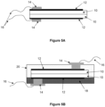
- the structure of the device is shown schematically in Figure 5A .
- the device comprises a pair of ionic liquid infiltrated Celgard membranes (10). On one side of each membrane is a film (12) printed from the ink described in Example 2. These printed films act as electrodes for the device. Electrical contacts were made with the electrodes using copper tape (14) and were connected to a voltage source by wires (16).
- FIG. 5B The structure of an alternate device, which comprises a substrate and a LDPE, IR-transparent protective layer, is shown in Figure 5B .
- the structure of the device in Figure 5B comprises an arrangement substantially as shown in Figure 5A .
- the device also comprises a PET substrate (18) and a protective encapsulation layer (20) formed from LDPE (low density polyethylene).
- Copper connectors (14) penetrate through the substrate (18) and protective layer (20) to allow for connection of the electrodes (12) to an external voltage/power source via wires (16).
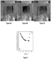
- Figures 6A to 6C shows the change of thermal emissivity of the device described in Example 3 on a hotplate at 55°C.
- Figures 6A to 6C were obtained using an FLIR C2 thermographic camera. The temperatures indicated at the top left of each Figure indicate the temperature measured at the circle displayed at the centre of each image.
- Figure 6A shows the device in Example 3 on a hotplate at 55°C with no potential difference applied to the device (i.e. with the device in a non-functioning state).
- Figure 6C shows the temperature of the device 10 seconds after the potential difference was removed from the device.
- Example 3 a device as described in Example 3 above was formed, but wherein the electrodes were formed solely from carbon nanotubes (rather than a combination of graphite nanoplatelets, carbon nanotubes and carboxymethylcellulose).
- the voltage applied to the device over the time period measured is shown at the top of the graph of Figure 8A.
- Figure 8A shows the measured temperature of a body placed behind the device (relative to the infrared temperature sensor).
- Figure 8A shows the ability for the device to modulate the apparent temperature of the body over a range of temperatures from 30°C to 100°C.
- Figure 8B shows the change in temperature (shown in Figure 8A ) as a function of the temperature of the body (whose temperature is being measured/modulated).
- Raman measurements were performed using a Renishaw inVia Qontor spectrometer with 488 nm (2.54 eV), 532 nm (2.33 eV), 660 nm (1.88 eV) and 785 nm (1.58 eV) laser sources. Acquisition powers ranged from 4-7 mW with 10 accumulations of 10 seconds. Multi-spectral Raman allows evaluation of nanotube diameter by focusing on the radial breathing modes (RBMs) in the range 152-192 cm -1 . The relationship between the RBM position and the diameter is slightly confounded by a bundling contribution, but it is estimated that the diameter of the carbon nanotubes in the films is between 1.1nm and 1.4 nm.
- Figure 9B shows the device when biased at -1V in the off state (near the maximum sheet resistance in Figure 9A ) and +2V in the on state (near the minimum sheet resistance) under an infrared camera with temperatures going from over sixty degrees to below 50 degrees.
- the time-temperature profile of the device at a variety of temperatures is shown in figure 1e.
- the temperature drop occurs over ⁇ 10 seconds on turning from 0V to +3V and similarly from going into the off state of -1V.
- the temperature drop is more pronounced as temperature increases due to the modulation of emissivity.
- Example 6 Device made from co-cast ionic liquid-infused polymeric membrane
- a further ink was prepared from 0.4 wt% single walled carbon nanotubes 0.4 wt% in water with 0.8 wt% sodium carboxymethyl cellulose, as purchased from OCSiAl.
- the carbon nanotube dispersion was diluted by a factor of 10 in deionised water and sonicated in a bath for 10 minutes to form a sprayable ink.
- the ink was then sprayed with an airbrush at 3 bar at a distance of 15 cm through an appropriate stencil to form a carbon nanotube-containing electrode layer. This was done on a hotplate at 90°C.
- a polymeric membrane was formed on top of the carbon nanotube-containing electrode layer by cocasting poly(vinylidene fluoride-co-hexafluoropropylene) (PVDF-HFP) with the ionic liquid [EMI][TMSI] to form a membrane having a thickness of 30 ⁇ m.
- PVDF-HFP poly(vinylidene fluoride-co-hexafluoropropylene)
- EMI][TMSI] ionic liquid
- a solid electrolyte precursor liquid comprising 1.94% (w/w) PVDF-HFP, 2.91% (w/w) [EMI][TFSI] and 95.15% (w/w) of acetone was dropcast at 200 ⁇ L per cm 2 onto the carbon nanotube-containing electrode later.
- the solvent was allowed to evaporate to leave a membrane comprising 60% [EMI][TSFI] and 40% PVDF-HDP.
- a second carbon nanotube-containing electrode layer was then formed on top of the polymeric membrane in a similar manner to the first carbon nanotube-containing electrode.
- the device was then constructed in an analogous manner to the device described in Example 3 above.
- the device described above was shown to possess similar properties to the device as described in Example 3 with regard to its ability to modify the apparent temperature of an object.
- Figure 10a shows 3 cycles of a cyclic voltammetry at 10 mV/s.
- the currents are largely stable with a box-like shape in the low potential range (-1 to +1 V).
- Figure 10b shows the apparent temperature of the device on a hot-plate at 70 °C as it is cycled. This again shows good thermal stability over the 3 cycles with a maximum temperature at -1V and a minimum around + 2.5V.
- Figure 10c shows the switching if the device between -1 and +2.5V 3 times. 90% of the switching occurs over the first 10 seconds after switching. This shows the viability of the device made in accordance with this example.
Landscapes
- Chemical & Material Sciences (AREA)
- Engineering & Computer Science (AREA)
- Materials Engineering (AREA)
- Nanotechnology (AREA)
- Organic Chemistry (AREA)
- Inorganic Chemistry (AREA)
- General Engineering & Computer Science (AREA)
- Carbon And Carbon Compounds (AREA)
- Lubricants (AREA)
- Battery Electrode And Active Subsutance (AREA)
Claims (15)
- Vorrichtung zur aktiven Modifikation der Wärmestrahlung, wobei die Vorrichtung Folgendes umfasst:(i) ein Substrat,(ii) eine oder mehrere permeable Polymermembranen, die einen ionischen flüssigen Elektrolyten umfassen;(iii) eine oder mehrere Elektroden, die Kohlenstoffnanoröhren umfassen, die auf der Oberfläche mindestens einer der einen oder mehreren Polymermembranen abgeschieden sind; und(iv) eine schützende Verkapselungsschicht.
- Vorrichtung nach Anspruch 1, wobei die eine oder mehreren Elektroden ferner Graphit-Nanoplättchen umfassen.
- Vorrichtung nach Anspruch 2, wobei die Kohlenstoffnanoröhren und Graphit-Nanoplättchen in den Elektroden in einem Gewichtsverhältnis von 0,15:1 bis 0,6:1 (Kohlenstoffnanoröhren:Graphit-Nanoplättchen) vorhanden sind.
- Vorrichtung nach einem der Ansprüche 1 bis 3, wobei die Polymermembran(en) zwischen einem Elektrodenpaar angeordnet ist/sind.
- Vorrichtung nach einem der Ansprüche 1 bis 4, umfassend einwandige Kohlenstoffnanoröhren, optional mit einem mittleren Durchmesser von 1 nm bis 5 nm und/oder einer Länge von mehr als 3 µm.
- Vorrichtung nach einem der Ansprüche 1 bis 5, wobei die Elektroden ferner ein Verdickungsmittel, zum Beispiel Carboxymethylcellulose, umfassen.
- Vorrichtung nach einem der Ansprüche 1 bis 6, wobei die Polymermembran Polyethylen, Polypropylen oder eine Mischung davon umfasst.
- Vorrichtung nach einem der Ansprüche 1 bis 7, wobei die ionische Flüssigkeit ein elektrochemisches Fenster von 4 V oder mehr aufweist.
- Vorrichtung nach einem der Ansprüche 1 bis 8, die an eine Stromquelle anschließbar oder angeschlossen ist.
- Vorrichtung nach Anspruch 1, umfassend:(i) eine oder mehrere permeable Polymermembranen, umfassend Polyethylen, Polypropylen oder eine Mischung davon, die eine ionische Flüssigkeit umfassen;(ii) eine oder mehrere Elektroden, die eine Mischung aus Graphen-Nanoplättchen und Kohlenstoffnanoröhren in einem Gewichtsverhältnis von 0,15:1 bis 0,6:1 (Kohlenstoffnanoröhren:Graphit-Nanoplättchen) umfassen und auf der Oberfläche mindestens einer der einen oder mehreren Polymermembranen abgeschieden sind.
- Vorrichtung nach Anspruch 1, umfassend:(i) eine oder mehrere permeable Polymermembranen, umfassend Polyethylen, Polypropylen oder eine Mischung davon, die eine ionische Flüssigkeit umfassen;(ii) ein Elektrodenpaar, das eine Mischung aus Kohlenstoffnanoröhren in einem Gewichtsverhältnis von 0,15:1 bis 0,6:1 (Kohlenstoffnanoröhren:Graphit-Nanoplättchen) umfasst, die auf der Oberfläche der einen oder mehreren Polymermembranen abgeschieden ist.
- Verfahren zur Herstellung einer Vorrichtung nach einem der Ansprüche 1 bis 11, wobei das Verfahren Folgendes umfasst:(a) Abscheiden einer flüssigen Zusammensetzung, die Kohlenstoffnanoröhren (und optional Graphit-Nanoplättchen) umfasst, auf mindestens einer von einer ersten und zweiten permeablen Polymermembran,(b) Imprägnieren der ersten und zweiten Polymermembran mit einer ionischen Flüssigkeit; und(c) Befestigen der ersten und zweiten Polymermembran aneinander.
- Verfahren zur Herstellung einer Vorrichtung nach einem der Ansprüche 1 bis 11, wobei das Verfahren Folgendes umfasst:(a) Bilden einer ersten und zweiten permeablen Polymermembran, die eine ionische Flüssigkeit umfassen;(b) Abscheiden einer flüssigen Zusammensetzung, die Kohlenstoffnanoröhren (und optional Graphit-Nanoplättchen) umfasst, auf mindestens einer (z. B. beiden) der Polymermembran, um einen Film zu bilden, der Kohlenstoffnanoröhren (und optional Graphit-Nanoplättchen) umfasst, und(c) Befestigen der ersten und zweiten Polymermembran aneinander.
- Verfahren zur Herstellung einer Vorrichtung nach einem der Ansprüche 1 bis 11, wobei das Verfahren Folgendes umfasst:(a) Bereitstellen eines Substrats;(b) Abscheiden einer flüssigen Zusammensetzung, die Kohlenstoffnanoröhren (und optional Graphit-Nanoplättchen) umfasst, auf dem Substrat, um eine erste Elektrode zu bilden,(c) Abscheiden einer Flüssigkeit, die ein Polymer und eine ionische Flüssigkeit umfasst, auf der ersten Elektrode, um eine permeable Polymermembran zu bilden, welche die ionische Flüssigkeit umfasst, und(d) Abscheiden einer flüssigen Zusammensetzung, die Kohlenstoffnanoröhren (und optional Graphit-Nanoplättchen) umfasst, auf der permeablen Polymermembran, um eine zweite Elektrode zu bilden.
- Verfahren zum Tarnen/Verbergen einer Wärmestrahlung eines Objekts, wobei das Verfahren Platzieren einer Vorrichtung nach einem der Ansprüche 1 bis 11 zwischen dem Objekt und einem Wärmestrahlungsdetektor umfasst.
Applications Claiming Priority (3)
| Application Number | Priority Date | Filing Date | Title |
|---|---|---|---|
| GBGB2103036.6A GB202103036D0 (en) | 2021-03-04 | 2021-03-04 | Devices with Low Thermal Emissivity |
| EP21171668.3A EP4053076A1 (de) | 2021-03-04 | 2021-04-30 | Eine vorrichtung zur aktiven modifikation der wärmestrahlung |
| PCT/EP2022/055483 WO2022184866A1 (en) | 2021-03-04 | 2022-03-03 | Devices with low thermal emissivity |
Publications (3)
| Publication Number | Publication Date |
|---|---|
| EP4301697A1 EP4301697A1 (de) | 2024-01-10 |
| EP4301697B1 true EP4301697B1 (de) | 2024-06-12 |
| EP4301697C0 EP4301697C0 (de) | 2024-06-12 |
Family
ID=80739073
Family Applications (1)
| Application Number | Title | Priority Date | Filing Date |
|---|---|---|---|
| EP22710092.2A Active EP4301697B1 (de) | 2021-03-04 | 2022-03-03 | Eine vorrichtung zur aktiven modifikation der wärmestrahlung |
Country Status (6)
| Country | Link |
|---|---|
| US (1) | US20240151498A1 (de) |
| EP (1) | EP4301697B1 (de) |
| AU (1) | AU2022229834A1 (de) |
| CA (1) | CA3210635A1 (de) |
| TW (1) | TW202306892A (de) |
| WO (1) | WO2022184866A1 (de) |
Family Cites Families (27)
| Publication number | Priority date | Publication date | Assignee | Title |
|---|---|---|---|---|
| US5312678A (en) * | 1989-10-06 | 1994-05-17 | The Dow Chemical Company | Camouflage material |
| US6759476B1 (en) * | 1999-07-14 | 2004-07-06 | Claude Q. C. Hayes | Flexible thermal control composite |
| US6338292B1 (en) * | 1999-09-30 | 2002-01-15 | Robert Fisher Reynolds | Thermal and visual camouflage system |
| JP2005532440A (ja) * | 2002-07-05 | 2005-10-27 | デグサ アクチエンゲゼルシャフト | ポリマーとイオン性液体とからなるポリマー組成物 |
| US20070009679A1 (en) * | 2005-05-25 | 2007-01-11 | Holcombe John D | Infrared suppressive material |
| US8340358B2 (en) * | 2008-04-24 | 2012-12-25 | Military Wraps Research And Development, Inc. | Visual camouflage with thermal and radar suppression and methods of making the same |
| US20100000441A1 (en) * | 2008-07-01 | 2010-01-07 | Jang Bor Z | Nano graphene platelet-based conductive inks |
| HUE044858T2 (hu) * | 2009-05-21 | 2019-11-28 | Polaris Solutions Ltd | Álcázó eszköz |
| US9765271B2 (en) * | 2012-06-27 | 2017-09-19 | James J. Myrick | Nanoparticles, compositions, manufacture and applications |
| US20170092975A1 (en) * | 2015-09-25 | 2017-03-30 | Samsung Electronics Co., Ltd. | Composite electrolyte film, electrochemical cell including the composite electrolyte film, and method of preparing the composite electrolyte film |
| GB201517784D0 (en) * | 2015-10-08 | 2015-11-25 | Univ Manchester | Production of graphene |
| EP3509835B1 (de) * | 2016-09-07 | 2022-03-16 | Warwick Mills, Inc. | Tarnlaminat mit feldanpassbarer verwaltung der visuellen und ir-signatur |
| EP3636592A1 (de) | 2018-10-12 | 2020-04-15 | Advanced Material Development Limited | Flüssigkeitsabschälende nanomaterialien |
| US11976162B2 (en) * | 2019-02-18 | 2024-05-07 | Arizona Board Of Regents On Behalf Of Arizona State University | Solvent-less ionic liquid epoxy resin |
| WO2020241388A1 (ja) * | 2019-05-29 | 2020-12-03 | 日本電気株式会社 | 放射抑制膜および放射抑制構造 |
| EP4038650A4 (de) * | 2019-10-04 | 2023-10-18 | Urbix, Inc. | Superkondensator mit vorspannungselektrode |
| CN114631202B (zh) * | 2019-11-15 | 2024-09-20 | 东丽株式会社 | 石墨烯分散液及正极糊料 |
| TW202140695A (zh) * | 2020-03-05 | 2021-11-01 | 英商先進材料發展有限公司 | 碳基導電墨水 |
| WO2021253302A1 (en) * | 2020-06-17 | 2021-12-23 | Guangdong Haozhi Technology Co. Limited | Conductive composition for secondary battery |
| KR102755854B1 (ko) * | 2020-04-22 | 2025-01-15 | 유미코아 | 배터리의 음극에서의 사용을 위한 분말 및 이러한 분말을 포함하는 배터리 |
| GB202006427D0 (en) * | 2020-04-30 | 2020-06-17 | Norwegian Univ Sci & Tech Ntnu | Gas separation membranes |
| CN114762145A (zh) * | 2020-06-17 | 2022-07-15 | 广东省皓智科技有限公司 | 用于二次电池中柔韧电极的浆料组合物 |
| CN114622405A (zh) * | 2020-12-14 | 2022-06-14 | 清华大学 | 红外隐身布料及红外隐身服装 |
| TW202323186A (zh) * | 2021-09-03 | 2023-06-16 | 英商先進材料發展有限公司 | 碳基導電墨水 |
| EP4459705A1 (de) * | 2021-12-30 | 2024-11-06 | Iucf-Hyu (Industry-University Cooperation Foundation Hanyang University) | Positivelektrode für lithium-schwefel-batterie, verfahren zur herstellung davon und lithium-schwefel-batterie damit |
| IL291528B2 (en) * | 2022-03-20 | 2023-07-01 | Ametrine Tech Ltd | Modular camouflage system and its use |
| US20240093968A1 (en) * | 2022-09-15 | 2024-03-21 | Stealth Labs, LLC | Omni-spectral thermal camouflage, signature mitigation and insulation apparatus, composition and system |
-
2022
- 2022-03-03 TW TW111107635A patent/TW202306892A/zh unknown
- 2022-03-03 AU AU2022229834A patent/AU2022229834A1/en active Pending
- 2022-03-03 EP EP22710092.2A patent/EP4301697B1/de active Active
- 2022-03-03 WO PCT/EP2022/055483 patent/WO2022184866A1/en not_active Ceased
- 2022-03-03 US US18/279,494 patent/US20240151498A1/en active Pending
- 2022-03-03 CA CA3210635A patent/CA3210635A1/en active Pending
Also Published As
| Publication number | Publication date |
|---|---|
| US20240151498A1 (en) | 2024-05-09 |
| EP4301697A1 (de) | 2024-01-10 |
| EP4301697C0 (de) | 2024-06-12 |
| AU2022229834A1 (en) | 2023-08-24 |
| CA3210635A1 (en) | 2022-09-09 |
| WO2022184866A1 (en) | 2022-09-09 |
| TW202306892A (zh) | 2023-02-16 |
Similar Documents
| Publication | Publication Date | Title |
|---|---|---|
| EP3805153B1 (de) | Kohlenstoffnanoröhrchen, kohlenstoffnanoröhrchenflüssigkeitsdispersion und verwendung davon | |
| Saha et al. | One-step hydrothermal synthesis of porous Ti 3 C 2 T z MXene/rGO gels for supercapacitor applications | |
| de Moraes et al. | Ion‐conductive, viscosity‐tunable hexagonal boron nitride nanosheet inks | |
| Li et al. | High-Performance Solid-State Supercapacitors and Microsupercapacitors Derived from Printable Graphene Inks. | |
| EP3816103B1 (de) | Kohlenstoffnanoröhrendispersion und ihre verwendung | |
| US12391843B2 (en) | Carbon-based conducting inks | |
| JP2024045445A (ja) | カーボンナノチューブ分散液およびその利用 | |
| Yazdi et al. | Direct Creation of Highly Conductive Laser‐Induced Graphene Nanocomposites from Polymer Blends | |
| KR101304190B1 (ko) | 전도도가 개선된 탄소나노튜브 투명전극 제조방법 | |
| Weng et al. | Preparation and characterizations of nanoparticles from graphite via an electrochemically oxidizing method | |
| AU2023332206A1 (en) | Devices for near-infrared signature reduction | |
| US20110287241A1 (en) | Graphene Tapes | |
| EP4053076A1 (de) | Eine vorrichtung zur aktiven modifikation der wärmestrahlung | |
| EP4301697B1 (de) | Eine vorrichtung zur aktiven modifikation der wärmestrahlung | |
| US20240384123A1 (en) | Carbon-based conducting inks | |
| Adu et al. | Flexible robust binder-free carbon nanotube membranes for solid state and microcapacitor application | |
| US12202986B2 (en) | Two-dimensional insulator based printable ion-conductive and viscosity-tunable inks, fabricating methods and applications of same | |
| Kataky et al. | Graphene oxide nanocapsules within silanized hydrogels suitable for electrochemical pseudocapacitors | |
| JP2024061527A (ja) | キャパシタ電極用スラリー、キャパシタ用電極、キャパシタ | |
| WO2025029560A1 (en) | Screen-printed microsupercapacitors enabled by hexagonal boron nitride ionogel electrolytes | |
| WO2020251638A2 (en) | Two-dimensional insulator based printable ion-conductive and viscosity-tunable inks, fabricating methods and applications of same | |
| EP4059034A1 (de) | Zusammensetzungen für energiespeichervorrichtungen und verwendungsverfahren | |
| Mevada et al. | Sustainable Energy Storage: 3d-Printed Catechin-Modified Activated Carbon Biodegradable Electrodes for Supercapacitors |
Legal Events
| Date | Code | Title | Description |
|---|---|---|---|
| STAA | Information on the status of an ep patent application or granted ep patent |
Free format text: STATUS: UNKNOWN |
|
| STAA | Information on the status of an ep patent application or granted ep patent |
Free format text: STATUS: THE INTERNATIONAL PUBLICATION HAS BEEN MADE |
|
| STAA | Information on the status of an ep patent application or granted ep patent |
Free format text: STATUS: EXAMINATION IS IN PROGRESS |
|
| PUAI | Public reference made under article 153(3) epc to a published international application that has entered the european phase |
Free format text: ORIGINAL CODE: 0009012 |
|
| 17P | Request for examination filed |
Effective date: 20230802 |
|
| AK | Designated contracting states |
Kind code of ref document: A1 Designated state(s): AL AT BE BG CH CY CZ DE DK EE ES FI FR GB GR HR HU IE IS IT LI LT LU LV MC MK MT NL NO PL PT RO RS SE SI SK SM TR |
|
| GRAP | Despatch of communication of intention to grant a patent |
Free format text: ORIGINAL CODE: EPIDOSNIGR1 |
|
| STAA | Information on the status of an ep patent application or granted ep patent |
Free format text: STATUS: GRANT OF PATENT IS INTENDED |
|
| DAV | Request for validation of the european patent (deleted) | ||
| DAX | Request for extension of the european patent (deleted) | ||
| INTG | Intention to grant announced |
Effective date: 20240216 |
|
| GRAS | Grant fee paid |
Free format text: ORIGINAL CODE: EPIDOSNIGR3 |
|
| GRAA | (expected) grant |
Free format text: ORIGINAL CODE: 0009210 |
|
| STAA | Information on the status of an ep patent application or granted ep patent |
Free format text: STATUS: THE PATENT HAS BEEN GRANTED |
|
| AK | Designated contracting states |
Kind code of ref document: B1 Designated state(s): AL AT BE BG CH CY CZ DE DK EE ES FI FR GB GR HR HU IE IS IT LI LT LU LV MC MK MT NL NO PL PT RO RS SE SI SK SM TR |
|
| REG | Reference to a national code |
Ref country code: GB Ref legal event code: FG4D |
|
| REG | Reference to a national code |
Ref country code: CH Ref legal event code: EP |
|
| REG | Reference to a national code |
Ref country code: IE Ref legal event code: FG4D |
|
| REG | Reference to a national code |
Ref country code: DE Ref legal event code: R096 Ref document number: 602022003949 Country of ref document: DE |
|
| U01 | Request for unitary effect filed |
Effective date: 20240618 |
|
| U07 | Unitary effect registered |
Designated state(s): AT BE BG DE DK EE FI FR IT LT LU LV MT NL PT RO SE SI Effective date: 20240902 |
|
| PG25 | Lapsed in a contracting state [announced via postgrant information from national office to epo] |
Ref country code: HR Free format text: LAPSE BECAUSE OF FAILURE TO SUBMIT A TRANSLATION OF THE DESCRIPTION OR TO PAY THE FEE WITHIN THE PRESCRIBED TIME-LIMIT Effective date: 20240612 |
|
| PG25 | Lapsed in a contracting state [announced via postgrant information from national office to epo] |
Ref country code: GR Free format text: LAPSE BECAUSE OF FAILURE TO SUBMIT A TRANSLATION OF THE DESCRIPTION OR TO PAY THE FEE WITHIN THE PRESCRIBED TIME-LIMIT Effective date: 20240913 |
|
| PG25 | Lapsed in a contracting state [announced via postgrant information from national office to epo] |
Ref country code: ES Free format text: LAPSE BECAUSE OF FAILURE TO SUBMIT A TRANSLATION OF THE DESCRIPTION OR TO PAY THE FEE WITHIN THE PRESCRIBED TIME-LIMIT Effective date: 20240612 |
|
| PG25 | Lapsed in a contracting state [announced via postgrant information from national office to epo] |
Ref country code: NO Free format text: LAPSE BECAUSE OF FAILURE TO SUBMIT A TRANSLATION OF THE DESCRIPTION OR TO PAY THE FEE WITHIN THE PRESCRIBED TIME-LIMIT Effective date: 20240912 Ref country code: HR Free format text: LAPSE BECAUSE OF FAILURE TO SUBMIT A TRANSLATION OF THE DESCRIPTION OR TO PAY THE FEE WITHIN THE PRESCRIBED TIME-LIMIT Effective date: 20240612 Ref country code: GR Free format text: LAPSE BECAUSE OF FAILURE TO SUBMIT A TRANSLATION OF THE DESCRIPTION OR TO PAY THE FEE WITHIN THE PRESCRIBED TIME-LIMIT Effective date: 20240913 Ref country code: ES Free format text: LAPSE BECAUSE OF FAILURE TO SUBMIT A TRANSLATION OF THE DESCRIPTION OR TO PAY THE FEE WITHIN THE PRESCRIBED TIME-LIMIT Effective date: 20240612 Ref country code: RS Free format text: LAPSE BECAUSE OF FAILURE TO SUBMIT A TRANSLATION OF THE DESCRIPTION OR TO PAY THE FEE WITHIN THE PRESCRIBED TIME-LIMIT Effective date: 20240912 |
|
| U1N | Appointed representative for the unitary patent procedure changed after the registration of the unitary effect |
Representative=s name: SCHLICH; GB |
|
| PG25 | Lapsed in a contracting state [announced via postgrant information from national office to epo] |
Ref country code: PL Free format text: LAPSE BECAUSE OF FAILURE TO SUBMIT A TRANSLATION OF THE DESCRIPTION OR TO PAY THE FEE WITHIN THE PRESCRIBED TIME-LIMIT Effective date: 20240612 |
|
| PG25 | Lapsed in a contracting state [announced via postgrant information from national office to epo] |
Ref country code: IS Free format text: LAPSE BECAUSE OF FAILURE TO SUBMIT A TRANSLATION OF THE DESCRIPTION OR TO PAY THE FEE WITHIN THE PRESCRIBED TIME-LIMIT Effective date: 20241012 |
|
| PG25 | Lapsed in a contracting state [announced via postgrant information from national office to epo] |
Ref country code: CZ Free format text: LAPSE BECAUSE OF FAILURE TO SUBMIT A TRANSLATION OF THE DESCRIPTION OR TO PAY THE FEE WITHIN THE PRESCRIBED TIME-LIMIT Effective date: 20240612 |
|
| PG25 | Lapsed in a contracting state [announced via postgrant information from national office to epo] |
Ref country code: SK Free format text: LAPSE BECAUSE OF FAILURE TO SUBMIT A TRANSLATION OF THE DESCRIPTION OR TO PAY THE FEE WITHIN THE PRESCRIBED TIME-LIMIT Effective date: 20240612 |
|
| PG25 | Lapsed in a contracting state [announced via postgrant information from national office to epo] |
Ref country code: SM Free format text: LAPSE BECAUSE OF FAILURE TO SUBMIT A TRANSLATION OF THE DESCRIPTION OR TO PAY THE FEE WITHIN THE PRESCRIBED TIME-LIMIT Effective date: 20240612 |
|
| PG25 | Lapsed in a contracting state [announced via postgrant information from national office to epo] |
Ref country code: SM Free format text: LAPSE BECAUSE OF FAILURE TO SUBMIT A TRANSLATION OF THE DESCRIPTION OR TO PAY THE FEE WITHIN THE PRESCRIBED TIME-LIMIT Effective date: 20240612 Ref country code: SK Free format text: LAPSE BECAUSE OF FAILURE TO SUBMIT A TRANSLATION OF THE DESCRIPTION OR TO PAY THE FEE WITHIN THE PRESCRIBED TIME-LIMIT Effective date: 20240612 Ref country code: PL Free format text: LAPSE BECAUSE OF FAILURE TO SUBMIT A TRANSLATION OF THE DESCRIPTION OR TO PAY THE FEE WITHIN THE PRESCRIBED TIME-LIMIT Effective date: 20240612 Ref country code: IS Free format text: LAPSE BECAUSE OF FAILURE TO SUBMIT A TRANSLATION OF THE DESCRIPTION OR TO PAY THE FEE WITHIN THE PRESCRIBED TIME-LIMIT Effective date: 20241012 Ref country code: CZ Free format text: LAPSE BECAUSE OF FAILURE TO SUBMIT A TRANSLATION OF THE DESCRIPTION OR TO PAY THE FEE WITHIN THE PRESCRIBED TIME-LIMIT Effective date: 20240612 |
|
| PLBE | No opposition filed within time limit |
Free format text: ORIGINAL CODE: 0009261 |
|
| STAA | Information on the status of an ep patent application or granted ep patent |
Free format text: STATUS: NO OPPOSITION FILED WITHIN TIME LIMIT |
|
| U20 | Renewal fee for the european patent with unitary effect paid |
Year of fee payment: 4 Effective date: 20250319 |
|
| 26N | No opposition filed |
Effective date: 20250313 |
|
| PG25 | Lapsed in a contracting state [announced via postgrant information from national office to epo] |
Ref country code: MC Free format text: LAPSE BECAUSE OF FAILURE TO SUBMIT A TRANSLATION OF THE DESCRIPTION OR TO PAY THE FEE WITHIN THE PRESCRIBED TIME-LIMIT Effective date: 20240612 |
|
| REG | Reference to a national code |
Ref country code: CH Ref legal event code: H13 Free format text: ST27 STATUS EVENT CODE: U-0-0-H10-H13 (AS PROVIDED BY THE NATIONAL OFFICE) Effective date: 20251023 |