EP4290771A1 - Mems-resonator und verarbeitungsverfahren für mems-resonator - Google Patents
Mems-resonator und verarbeitungsverfahren für mems-resonator Download PDFInfo
- Publication number
- EP4290771A1 EP4290771A1 EP22770373.3A EP22770373A EP4290771A1 EP 4290771 A1 EP4290771 A1 EP 4290771A1 EP 22770373 A EP22770373 A EP 22770373A EP 4290771 A1 EP4290771 A1 EP 4290771A1
- Authority
- EP
- European Patent Office
- Prior art keywords
- layer
- barrier layer
- mems resonator
- harmonic oscillator
- conducting
- Prior art date
- Legal status (The legal status is an assumption and is not a legal conclusion. Google has not performed a legal analysis and makes no representation as to the accuracy of the status listed.)
- Pending
Links
- 238000003672 processing method Methods 0.000 title claims description 22
- 230000004888 barrier function Effects 0.000 claims abstract description 194
- 238000002955 isolation Methods 0.000 claims abstract description 159
- KRHYYFGTRYWZRS-UHFFFAOYSA-N Fluorane Chemical compound F KRHYYFGTRYWZRS-UHFFFAOYSA-N 0.000 claims abstract description 52
- 239000000758 substrate Substances 0.000 claims abstract description 48
- 239000010410 layer Substances 0.000 claims description 499
- 239000000463 material Substances 0.000 claims description 45
- 239000003990 capacitor Substances 0.000 claims description 25
- 230000005284 excitation Effects 0.000 claims description 17
- 238000005530 etching Methods 0.000 claims description 16
- 239000011241 protective layer Substances 0.000 claims description 16
- 238000000151 deposition Methods 0.000 claims description 14
- VYPSYNLAJGMNEJ-UHFFFAOYSA-N Silicium dioxide Chemical compound O=[Si]=O VYPSYNLAJGMNEJ-UHFFFAOYSA-N 0.000 claims description 13
- 229910021420 polycrystalline silicon Inorganic materials 0.000 claims description 13
- 229910052814 silicon oxide Inorganic materials 0.000 claims description 13
- 229910021417 amorphous silicon Inorganic materials 0.000 claims description 9
- 230000010355 oscillation Effects 0.000 claims description 6
- PNEYBMLMFCGWSK-UHFFFAOYSA-N aluminium oxide Inorganic materials [O-2].[O-2].[O-2].[Al+3].[Al+3] PNEYBMLMFCGWSK-UHFFFAOYSA-N 0.000 claims description 4
- 229910052593 corundum Inorganic materials 0.000 claims description 4
- TWNQGVIAIRXVLR-UHFFFAOYSA-N oxo(oxoalumanyloxy)alumane Chemical group O=[Al]O[Al]=O TWNQGVIAIRXVLR-UHFFFAOYSA-N 0.000 claims description 4
- 229910001845 yogo sapphire Inorganic materials 0.000 claims description 4
- 239000012212 insulator Substances 0.000 claims description 3
- XUIMIQQOPSSXEZ-UHFFFAOYSA-N Silicon Chemical compound [Si] XUIMIQQOPSSXEZ-UHFFFAOYSA-N 0.000 description 50
- 229910052710 silicon Inorganic materials 0.000 description 50
- 239000010703 silicon Substances 0.000 description 50
- 238000000034 method Methods 0.000 description 17
- 238000010586 diagram Methods 0.000 description 15
- 238000001514 detection method Methods 0.000 description 12
- 229910052751 metal Inorganic materials 0.000 description 7
- 239000002184 metal Substances 0.000 description 7
- 238000005260 corrosion Methods 0.000 description 6
- 230000007797 corrosion Effects 0.000 description 6
- 238000004518 low pressure chemical vapour deposition Methods 0.000 description 6
- 230000008569 process Effects 0.000 description 5
- XLOMVQKBTHCTTD-UHFFFAOYSA-N Zinc monoxide Chemical compound [Zn]=O XLOMVQKBTHCTTD-UHFFFAOYSA-N 0.000 description 4
- 238000005240 physical vapour deposition Methods 0.000 description 4
- BASFCYQUMIYNBI-UHFFFAOYSA-N platinum Chemical compound [Pt] BASFCYQUMIYNBI-UHFFFAOYSA-N 0.000 description 4
- 229910052782 aluminium Inorganic materials 0.000 description 3
- XAGFODPZIPBFFR-UHFFFAOYSA-N aluminium Chemical compound [Al] XAGFODPZIPBFFR-UHFFFAOYSA-N 0.000 description 3
- 238000005229 chemical vapour deposition Methods 0.000 description 3
- 230000003647 oxidation Effects 0.000 description 3
- 238000007254 oxidation reaction Methods 0.000 description 3
- ZOKXTWBITQBERF-UHFFFAOYSA-N Molybdenum Chemical compound [Mo] ZOKXTWBITQBERF-UHFFFAOYSA-N 0.000 description 2
- RTAQQCXQSZGOHL-UHFFFAOYSA-N Titanium Chemical compound [Ti] RTAQQCXQSZGOHL-UHFFFAOYSA-N 0.000 description 2
- 238000000231 atomic layer deposition Methods 0.000 description 2
- 238000004590 computer program Methods 0.000 description 2
- PMHQVHHXPFUNSP-UHFFFAOYSA-M copper(1+);methylsulfanylmethane;bromide Chemical compound Br[Cu].CSC PMHQVHHXPFUNSP-UHFFFAOYSA-M 0.000 description 2
- 238000013016 damping Methods 0.000 description 2
- 230000008021 deposition Effects 0.000 description 2
- 239000007789 gas Substances 0.000 description 2
- 229910052750 molybdenum Inorganic materials 0.000 description 2
- 239000011733 molybdenum Substances 0.000 description 2
- 229910052697 platinum Inorganic materials 0.000 description 2
- 238000005498 polishing Methods 0.000 description 2
- 239000004065 semiconductor Substances 0.000 description 2
- 239000000126 substance Substances 0.000 description 2
- 229910052719 titanium Inorganic materials 0.000 description 2
- 239000010936 titanium Substances 0.000 description 2
- 239000011787 zinc oxide Substances 0.000 description 2
- JBRZTFJDHDCESZ-UHFFFAOYSA-N AsGa Chemical compound [As]#[Ga] JBRZTFJDHDCESZ-UHFFFAOYSA-N 0.000 description 1
- 229910001218 Gallium arsenide Inorganic materials 0.000 description 1
- 229910000530 Gallium indium arsenide Inorganic materials 0.000 description 1
- 238000000137 annealing Methods 0.000 description 1
- 239000003963 antioxidant agent Substances 0.000 description 1
- 230000003078 antioxidant effect Effects 0.000 description 1
- QVGXLLKOCUKJST-UHFFFAOYSA-N atomic oxygen Chemical compound [O] QVGXLLKOCUKJST-UHFFFAOYSA-N 0.000 description 1
- 229910010293 ceramic material Inorganic materials 0.000 description 1
- 230000008859 change Effects 0.000 description 1
- 238000006243 chemical reaction Methods 0.000 description 1
- 239000004020 conductor Substances 0.000 description 1
- 238000002425 crystallisation Methods 0.000 description 1
- 230000008025 crystallization Effects 0.000 description 1
- 230000000694 effects Effects 0.000 description 1
- 229910052732 germanium Inorganic materials 0.000 description 1
- GNPVGFCGXDBREM-UHFFFAOYSA-N germanium atom Chemical compound [Ge] GNPVGFCGXDBREM-UHFFFAOYSA-N 0.000 description 1
- RPQDHPTXJYYUPQ-UHFFFAOYSA-N indium arsenide Chemical compound [In]#[As] RPQDHPTXJYYUPQ-UHFFFAOYSA-N 0.000 description 1
- UJXZVRRCKFUQKG-UHFFFAOYSA-K indium(3+);phosphate Chemical compound [In+3].[O-]P([O-])([O-])=O UJXZVRRCKFUQKG-UHFFFAOYSA-K 0.000 description 1
- HFGPZNIAWCZYJU-UHFFFAOYSA-N lead zirconate titanate Chemical compound [O-2].[O-2].[O-2].[O-2].[O-2].[Ti+4].[Zr+4].[Pb+2] HFGPZNIAWCZYJU-UHFFFAOYSA-N 0.000 description 1
- GQYHUHYESMUTHG-UHFFFAOYSA-N lithium niobate Chemical compound [Li+].[O-][Nb](=O)=O GQYHUHYESMUTHG-UHFFFAOYSA-N 0.000 description 1
- 238000001755 magnetron sputter deposition Methods 0.000 description 1
- 239000001301 oxygen Substances 0.000 description 1
- 229910052760 oxygen Inorganic materials 0.000 description 1
- 238000012536 packaging technology Methods 0.000 description 1
- 238000007517 polishing process Methods 0.000 description 1
- 239000002861 polymer material Substances 0.000 description 1
- 238000007789 sealing Methods 0.000 description 1
- HBMJWWWQQXIZIP-UHFFFAOYSA-N silicon carbide Chemical compound [Si+]#[C-] HBMJWWWQQXIZIP-UHFFFAOYSA-N 0.000 description 1
- 229910010271 silicon carbide Inorganic materials 0.000 description 1
- 239000002210 silicon-based material Substances 0.000 description 1
- 239000010409 thin film Substances 0.000 description 1
- 238000009461 vacuum packaging Methods 0.000 description 1
Images








Classifications
-
- H—ELECTRICITY
- H03—ELECTRONIC CIRCUITRY
- H03H—IMPEDANCE NETWORKS, e.g. RESONANT CIRCUITS; RESONATORS
- H03H3/00—Apparatus or processes specially adapted for the manufacture of impedance networks, resonating circuits, resonators
- H03H3/007—Apparatus or processes specially adapted for the manufacture of impedance networks, resonating circuits, resonators for the manufacture of electromechanical resonators or networks
-
- H—ELECTRICITY
- H03—ELECTRONIC CIRCUITRY
- H03H—IMPEDANCE NETWORKS, e.g. RESONANT CIRCUITS; RESONATORS
- H03H3/00—Apparatus or processes specially adapted for the manufacture of impedance networks, resonating circuits, resonators
- H03H3/007—Apparatus or processes specially adapted for the manufacture of impedance networks, resonating circuits, resonators for the manufacture of electromechanical resonators or networks
- H03H3/0072—Apparatus or processes specially adapted for the manufacture of impedance networks, resonating circuits, resonators for the manufacture of electromechanical resonators or networks of microelectro-mechanical resonators or networks
-
- H—ELECTRICITY
- H03—ELECTRONIC CIRCUITRY
- H03H—IMPEDANCE NETWORKS, e.g. RESONANT CIRCUITS; RESONATORS
- H03H9/00—Networks comprising electromechanical or electro-acoustic elements; Electromechanical resonators
- H03H9/02—Details
- H03H9/02244—Details of microelectro-mechanical resonators
- H03H9/02433—Means for compensation or elimination of undesired effects
-
- H—ELECTRICITY
- H03—ELECTRONIC CIRCUITRY
- H03H—IMPEDANCE NETWORKS, e.g. RESONANT CIRCUITS; RESONATORS
- H03H3/00—Apparatus or processes specially adapted for the manufacture of impedance networks, resonating circuits, resonators
- H03H3/007—Apparatus or processes specially adapted for the manufacture of impedance networks, resonating circuits, resonators for the manufacture of electromechanical resonators or networks
- H03H3/0072—Apparatus or processes specially adapted for the manufacture of impedance networks, resonating circuits, resonators for the manufacture of electromechanical resonators or networks of microelectro-mechanical resonators or networks
- H03H3/0073—Integration with other electronic structures
-
- H—ELECTRICITY
- H03—ELECTRONIC CIRCUITRY
- H03H—IMPEDANCE NETWORKS, e.g. RESONANT CIRCUITS; RESONATORS
- H03H9/00—Networks comprising electromechanical or electro-acoustic elements; Electromechanical resonators
- H03H9/02—Details
- H03H9/02244—Details of microelectro-mechanical resonators
- H03H9/02393—Post-fabrication trimming of parameters, e.g. resonance frequency, Q factor
- H03H9/02409—Post-fabrication trimming of parameters, e.g. resonance frequency, Q factor by application of a DC-bias voltage
-
- H—ELECTRICITY
- H03—ELECTRONIC CIRCUITRY
- H03H—IMPEDANCE NETWORKS, e.g. RESONANT CIRCUITS; RESONATORS
- H03H9/00—Networks comprising electromechanical or electro-acoustic elements; Electromechanical resonators
- H03H9/02—Details
- H03H9/05—Holders or supports
- H03H9/0595—Holders or supports the holder support and resonator being formed in one body
-
- H—ELECTRICITY
- H03—ELECTRONIC CIRCUITRY
- H03H—IMPEDANCE NETWORKS, e.g. RESONANT CIRCUITS; RESONATORS
- H03H9/00—Networks comprising electromechanical or electro-acoustic elements; Electromechanical resonators
- H03H9/02—Details
- H03H9/05—Holders or supports
- H03H9/10—Mounting in enclosures
- H03H9/1007—Mounting in enclosures for bulk acoustic wave [BAW] devices
- H03H9/1014—Mounting in enclosures for bulk acoustic wave [BAW] devices the enclosure being defined by a frame built on a substrate and a cap, the frame having no mechanical contact with the BAW device
- H03H9/1021—Mounting in enclosures for bulk acoustic wave [BAW] devices the enclosure being defined by a frame built on a substrate and a cap, the frame having no mechanical contact with the BAW device the BAW device being of the cantilever type
-
- H—ELECTRICITY
- H03—ELECTRONIC CIRCUITRY
- H03H—IMPEDANCE NETWORKS, e.g. RESONANT CIRCUITS; RESONATORS
- H03H9/00—Networks comprising electromechanical or electro-acoustic elements; Electromechanical resonators
- H03H9/02—Details
- H03H9/05—Holders or supports
- H03H9/10—Mounting in enclosures
- H03H9/1057—Mounting in enclosures for microelectro-mechanical devices
-
- H—ELECTRICITY
- H03—ELECTRONIC CIRCUITRY
- H03H—IMPEDANCE NETWORKS, e.g. RESONANT CIRCUITS; RESONATORS
- H03H9/00—Networks comprising electromechanical or electro-acoustic elements; Electromechanical resonators
- H03H9/24—Constructional features of resonators of material which is not piezoelectric, electrostrictive, or magnetostrictive
-
- H—ELECTRICITY
- H03—ELECTRONIC CIRCUITRY
- H03H—IMPEDANCE NETWORKS, e.g. RESONANT CIRCUITS; RESONATORS
- H03H9/00—Networks comprising electromechanical or electro-acoustic elements; Electromechanical resonators
- H03H9/24—Constructional features of resonators of material which is not piezoelectric, electrostrictive, or magnetostrictive
- H03H9/2405—Constructional features of resonators of material which is not piezoelectric, electrostrictive, or magnetostrictive of microelectro-mechanical resonators
- H03H9/2447—Beam resonators
- H03H9/2463—Clamped-clamped beam resonators
-
- H—ELECTRICITY
- H03—ELECTRONIC CIRCUITRY
- H03H—IMPEDANCE NETWORKS, e.g. RESONANT CIRCUITS; RESONATORS
- H03H9/00—Networks comprising electromechanical or electro-acoustic elements; Electromechanical resonators
- H03H9/46—Filters
- H03H9/462—Microelectro-mechanical filters
- H03H9/465—Microelectro-mechanical filters in combination with other electronic elements
-
- H—ELECTRICITY
- H03—ELECTRONIC CIRCUITRY
- H03H—IMPEDANCE NETWORKS, e.g. RESONANT CIRCUITS; RESONATORS
- H03H9/00—Networks comprising electromechanical or electro-acoustic elements; Electromechanical resonators
- H03H9/46—Filters
- H03H9/462—Microelectro-mechanical filters
- H03H9/467—Post-fabrication trimming of parameters, e.g. center frequency
-
- H—ELECTRICITY
- H03—ELECTRONIC CIRCUITRY
- H03H—IMPEDANCE NETWORKS, e.g. RESONANT CIRCUITS; RESONATORS
- H03H9/00—Networks comprising electromechanical or electro-acoustic elements; Electromechanical resonators
- H03H9/46—Filters
- H03H9/54—Filters comprising resonators of piezoelectric or electrostrictive material
- H03H9/542—Filters comprising resonators of piezoelectric or electrostrictive material including passive elements
-
- H—ELECTRICITY
- H03—ELECTRONIC CIRCUITRY
- H03B—GENERATION OF OSCILLATIONS, DIRECTLY OR BY FREQUENCY-CHANGING, BY CIRCUITS EMPLOYING ACTIVE ELEMENTS WHICH OPERATE IN A NON-SWITCHING MANNER; GENERATION OF NOISE BY SUCH CIRCUITS
- H03B5/00—Generation of oscillations using amplifier with regenerative feedback from output to input
- H03B5/30—Generation of oscillations using amplifier with regenerative feedback from output to input with frequency-determining element being electromechanical resonator
- H03B5/32—Generation of oscillations using amplifier with regenerative feedback from output to input with frequency-determining element being electromechanical resonator being a piezoelectric resonator
-
- H—ELECTRICITY
- H03—ELECTRONIC CIRCUITRY
- H03H—IMPEDANCE NETWORKS, e.g. RESONANT CIRCUITS; RESONATORS
- H03H3/00—Apparatus or processes specially adapted for the manufacture of impedance networks, resonating circuits, resonators
- H03H3/007—Apparatus or processes specially adapted for the manufacture of impedance networks, resonating circuits, resonators for the manufacture of electromechanical resonators or networks
- H03H3/02—Apparatus or processes specially adapted for the manufacture of impedance networks, resonating circuits, resonators for the manufacture of electromechanical resonators or networks for the manufacture of piezoelectric or electrostrictive resonators or networks
- H03H2003/022—Apparatus or processes specially adapted for the manufacture of impedance networks, resonating circuits, resonators for the manufacture of electromechanical resonators or networks for the manufacture of piezoelectric or electrostrictive resonators or networks the resonators or networks being of the cantilever type
-
- H—ELECTRICITY
- H03—ELECTRONIC CIRCUITRY
- H03H—IMPEDANCE NETWORKS, e.g. RESONANT CIRCUITS; RESONATORS
- H03H9/00—Networks comprising electromechanical or electro-acoustic elements; Electromechanical resonators
- H03H9/02—Details
- H03H9/02007—Details of bulk acoustic wave devices
- H03H9/02157—Dimensional parameters, e.g. ratio between two dimension parameters, length, width or thickness
-
- H—ELECTRICITY
- H03—ELECTRONIC CIRCUITRY
- H03H—IMPEDANCE NETWORKS, e.g. RESONANT CIRCUITS; RESONATORS
- H03H9/00—Networks comprising electromechanical or electro-acoustic elements; Electromechanical resonators
- H03H9/02—Details
- H03H9/02244—Details of microelectro-mechanical resonators
- H03H9/02259—Driving or detection means
Definitions
- This application relates to the field of clock devices, and in particular, to a MEMS resonator and a MEMS resonator processing method.
- micro electro mechanical system Micro Electro Mechanical System, MEMS
- MEMS Micro Electro Mechanical System
- MEMS devices have stricter requirements on packaging technologies.
- vacuum packaging is performed on a harmonic oscillator in the MEMS resonator to reduce an air damping loss of the harmonic oscillator, thereby increasing a quality factor (quality factor, Q) value of the harmonic oscillator.
- a sacrificial layer originally exists in a vacuum cavity, serving as a support during processing.
- breather holes are etched on an upper cavity wall of the vacuum cavity. Hydrofluoric acid vapor is injected through the breather holes to corrode the sacrificial layer to form the vacuum cavity.
- a size of the vacuum cavity is directly proportional to duration of corrosion.
- This application provides a MEMS resonator and a MEMS resonator processing method.
- a first electrical isolation structure and a cavity are isolated by using a barrier layer and a dielectric isolation layer, to prevent hydrofluoric acid vapor from corroding the first electrical isolation structure, and improve a yield of the MEMS resonator.
- a first aspect of this application provides a MEMS resonator.
- the MEMS resonator includes a substrate, a barrier layer, a conducting layer, a dielectric isolation layer, a harmonic oscillator, a first electrical isolation structure, and a first conducting structure.
- the substrate and the barrier layer are combined to form a cavity, a junction between the substrate and the barrier layer includes the conducting layer, the dielectric isolation layer is included between the conducting layer and the barrier layer, and the dielectric isolation layer is configured to isolate electrical connection between the conducting layer and the barrier layer.
- the harmonic oscillator is connected to the conducting layer and is suspended in the cavity.
- the conducting layer is connected to the first conducting structure that is outside the barrier layer.
- the first conducting structure may provide excitation for the harmonic oscillator, so that the harmonic oscillator in the harmonic oscillator vibrates in the cavity.
- the first electrical isolation structure is included between the first conducting structure and the barrier layer.
- the first electrical isolation structure is configured to isolate electrical connection between the first conducting structure and the barrier layer.
- the barrier layer and the dielectric isolation layer are configured to isolate the first electrical isolation structure from the cavity.
- the first electrical isolation structure and the cavity are isolated by using the barrier layer and the dielectric isolation layer, to prevent hydrofluoric acid vapor from corroding the first electrical isolation structure, thereby reducing a probability of a short circuit and improving a yield of the MEMS resonator.
- a material of the barrier layer may be a conductive material, such as polycrystalline silicon or amorphous silicon.
- the barrier layer includes a first barrier layer and a second barrier layer. Breather holes are disposed on the first barrier layer. During processing of the MEMS resonator, hydrofluoric acid vapor may be injected through the breather holes to corrode a sacrificial layer in the original cavity.
- the second barrier layer is configured to seal the breather holes to seal the harmonic oscillator in the cavity. Therefore, this can effectively reduce an air damping loss of the harmonic oscillator, thereby increasing a Q value of the harmonic oscillator.
- a material of the second barrier layer is polycrystalline silicon or amorphous silicon.
- polycrystalline silicon or amorphous silicon is formed at a high temperature, residual gas in the cavity can be removed, thereby increasing a Q value of the MEMS resonator.
- a material of the first barrier layer is different from a material of the first electrical isolation structure.
- the first electrical isolation structure for example, silicon oxide, is corroded by hydrofluoric acid vapor.
- the first barrier layer is exposed to the hydrofluoric acid vapor directly, to prevent the hydrofluoric acid vapor from corroding the first electrical isolation structure. Therefore, the material of the first electrical isolation and the material of the first barrier layer are defined to be different.
- the material of the second barrier layer is the same as the material of the first barrier layer.
- the second barrier layer is configured to seal the breather holes on the first barrier layer.
- sealing performance can be improved.
- the harmonic oscillator includes an upper electrode layer, a piezoelectric layer, and a lower electrode layer, and the piezoelectric layer is located between the upper electrode layer and the lower electrode layer.
- materials of the upper electrode layer and the piezoelectric layer may be oxidized at the high temperature.
- the dielectric isolation layer covers the upper electrode layer and the piezoelectric layer, to protect the upper electrode layer and the piezoelectric layer. Therefore, this application can improve flexibility of drive detection and frequency modulation of the MEMS resonator.
- a material of the dielectric isolation layer is aluminum oxide Al 2 O 3 .
- a thickness of the dielectric isolation layer is 0.01 ⁇ m to 2 ⁇ m.
- the MEMS resonator further includes a functional electrode, and the functional electrode and the harmonic oscillator form a capacitor.
- the harmonic oscillator When a direct current bias voltage is applied to the functional electrode, the harmonic oscillator generates an offset in a fixed direction. When the harmonic oscillator generates an offset, a resonance frequency of the harmonic oscillator changes.
- the functional electrode is disposed, to implement frequency adjustment of the harmonic oscillator.
- the functional electrode includes a first functional electrode and a second functional electrode.
- the first functional electrode and the harmonic oscillator form a first capacitor
- the second functional electrode and the harmonic oscillator form a second capacitor.
- the first capacitor and the second capacitor are distributed symmetric about the harmonic oscillator.
- the two symmetric functional electrodes are disposed to increase an offset amount of the harmonic oscillator, thereby expanding a range of frequency adjustment of the harmonic oscillator
- the functional electrode is connected to a second conducting structure that is outside the barrier layer, and a second electrical isolation structure is included between the second conducting structure and the barrier layer.
- the barrier layer and the dielectric isolation layer are configured to isolate the second electrical isolation structure from the cavity.
- the second electrical isolation structure and the cavity are isolated by using the barrier layer and the dielectric isolation layer, to prevent hydrofluoric acid vapor from corroding the second electrical isolation structure, thereby reducing a probability of a short circuit and improving a yield of the MEMS resonator.
- the harmonic oscillator vibrates based on the alternating current voltage.
- the alternating current voltage is used as vibration excitation of the harmonic oscillator, which is briefly referred to as electrostatic excitation.
- a voltage applied to the upper electrode layer may be used to perform detection on a vibration frequency of the harmonic oscillator, which is briefly referred to as piezoelectric detection. Through piezoelectric detection, it can be determined whether the vibration frequency of the harmonic oscillator meets an expected frequency. Therefore, in this application, reliability of the MEMS resonator can be improved through piezoelectric detection.
- the MEMS resonator further includes a support beam.
- the harmonic oscillator is connected to the conducting layer through the support beam and is suspended in the cavity.
- a material of the functional electrode is the same as a material of the lower electrode layer of the harmonic oscillator.
- processing steps of the MEMS resonator can be reduced, thereby reducing processing costs.
- the MEMS resonator further includes a protective layer above the barrier layer.
- an electrical through-hole is disposed on the protective layer, and an electrode pad is deposited on the electrical through-hole.
- the electrode pad is connected to the first conducting structure.
- a silicon oxide layer is included on a surface of the substrate.
- the silicon oxide layer is added to isolate electrical connection between the harmonic oscillator and the substrate. This reduces a probability of electric leakage, and improves reliability of the MEMS resonator.
- a processing temperature of the second barrier layer is greater than 500 degrees Celsius.
- the processing temperature may be a temperature in an epitaxial growth process, or may be a temperature in a crystallization process.
- the second barrier layer may be obtained by epitaxially growing polycrystalline silicon in a high-temperature environment.
- the second barrier layer of polycrystalline silicon may be obtained by epitaxially growing amorphous silicon and then annealing the amorphous silicon at a high temperature to crystallize.
- a second aspect of this application provides a MEMS resonator processing method.
- the method includes: providing a silicon-on-insulator (Silicon on insulator, SOI) wafer including a substrate and a conducting layer; etching the conducting layer to form a harmonic oscillator and a support beam, where the harmonic oscillator is connected to the conducting layer through the support beam; depositing a dielectric isolation layer and a sacrificial layer on the conducting layer; etching the sacrificial layer, and epitaxially growing or depositing a first barrier layer on the sacrificial layer, so that the harmonic oscillator is located in an area formed by the first barrier layer and the substrate; etching breather holes on the first barrier layer; injecting hydrofluoric acid vapor through the breather holes to corrode the sacrificial layer in the area, so that the harmonic oscillator is suspended, through the support beam, in a cavity formed by the area; and epitaxially growing a second barrier layer on the first barrier layer
- a material of the second barrier layer is polycrystalline silicon or amorphous silicon.
- a material of the first barrier layer is different from a material of the first electrical isolation structure.
- the material of the second barrier layer is the same as the material of the first barrier layer
- the method further includes: generating a piezoelectric layer on the conducting layer, and depositing an upper electrode layer on the piezoelectric layer.
- the dielectric isolation layer covers the upper electrode layer and the piezoelectric layer of the harmonic oscillator.
- a material of the dielectric isolation layer is aluminum oxide Al 2 O 3 .
- a thickness of the dielectric isolation layer is 0.01 ⁇ m to 2 ⁇ m.
- the MEMS resonator further includes a functional electrode, and the functional electrode and the harmonic oscillator form a capacitor.
- the harmonic oscillator When a direct current bias voltage is applied to the functional electrode, the harmonic oscillator generates an offset in a fixed direction.
- the functional electrode includes a first functional electrode and a second functional electrode.
- the first functional electrode and the harmonic oscillator form a first capacitor.
- the second functional electrode and the harmonic oscillator form a second capacitor.
- the first capacitor and the second capacitor are distributed symmetric about the harmonic oscillator.
- the conducting layer is connected to a first conducting structure that is outside the barrier layer, a first electrical isolation structure is included between the first conducting structure and the barrier layer, and the barrier layer and the dielectric isolation layer are configured to isolate the first electrical isolation structure from the cavity.
- a material of the functional electrode is the same as a material of the lower electrode layer of the harmonic oscillator
- the method further includes: depositing a protective layer on the barrier layer.
- the method further includes: etching an electrical through-hole on the protective layer, and depositing an electrode pad on the electrical through-hole.
- a processing temperature of the second barrier layer is greater than 500 degrees Celsius.
- a third aspect of this application provides a clock device.
- the clock device includes a MEMS resonator and a maintaining circuit.
- the maintaining circuit provides closed-loop oscillation excitation for the MEMS resonator.
- the MEMS resonator generates a clock signal through oscillation excitation.
- the MEMS resonator is the MEMS resonator according to the foregoing first aspect.
- a fourth aspect of this application provides a terminal.
- the terminal includes a clock device and a processor.
- the clock device is configured to provide a clock signal for the processor.
- the processor performs operation processing based on the clock signal.
- the clock device is the clock device according to the foregoing third aspect.
- a fifth aspect of this application provides a computer storage medium.
- the computer storage medium stores instructions.
- the instructions When executed on a computer, the computer is enabled to perform the method according to the second aspect or any one of the implementations of the second aspect.
- a sixth aspect of this application provides a computer program product.
- the computer program product When the computer product is executed on a computer, the computer is enabled to perform the method according to the second aspect or any one of the implementations of the second aspect.
- This application provides a MEMS resonator and a MEMS resonator processing method, applied to the field of clock devices.
- a first electrical isolation structure and a cavity are isolated by using a barrier layer and a dielectric isolation layer, to prevent hydrofluoric acid vapor from corroding the first electrical isolation structure, and improve a yield of the MEMS resonator.
- each processing step and/or component of the MEMS resonator may merely be briefly described in this application.
- different processing steps and/or components for achieving a same purpose may be interchanged. Therefore, specific examples of processing steps and/or components are described in this application to simplify the technical solutions disclosed in this application. Certainly, these examples are not intended to impose a limitation.
- reference numbers and/or letters are repeated in embodiments of this application. Repetition does not indicate that there is a strict restrictive relationship between various embodiments and/or configurations.
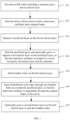
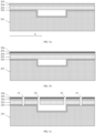
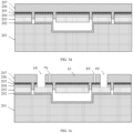
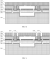
- FIG. 1 is a schematic flowchart of a MEMS resonator processing method according to this application. To facilitate description of the MEMS resonator processing method, corresponding descriptions are provided subsequently with reference to schematic diagrams of a structure of a MEMS resonator in different processing stages. Specifically, FIG. 2a to FIG. 21 are schematic diagrams of a structure of a MEMS resonator in different processing stages according to this application. As shown in FIG. 1 , the processing method includes the following steps.
- Step 101 Provide an SOI wafer including a substrate and a device silicon layer.
- the SOI wafer is also referred to as a carrier wafer, and the carrier wafer is a silicon wafer.
- an SOI wafer includes a substrate 201, a silicon oxide layer 202, and a device silicon layer 203.
- the silicon oxide layer 202 is located between the substrate 201 and the device silicon layer 203, and is configured to implement electrical isolation between the substrate 201 and the device silicon layer 203.
- the silicon oxide layer 202 may be silicon oxide obtained through thermal oxidation. Compared with silicon oxide obtained through chemical vapor deposition (Chemical Vapor Deposition, CVD), the silicon oxide obtained through thermal oxidation has higher density and is not easy to corrode.
- the substrate 201 is also referred to as a base.
- Materials of the substrate 201 and the device silicon layer 203 may be the same or may be different.
- materials of the substrate 201 and the device silicon layer 203 may be Si-based materials, ceramic materials, or polymer materials.
- the substrate 201 and the device silicon layer 203 may further include other-element (such as germanium) semiconductors or other-compound (such as silicon carbide, gallium arsenide, indium arsenide, and indium phosphate) semiconductors. Because materials of the substrate 201 and the device silicon layer 203 do not affect implementation of the technical solutions, the materials of the substrate 201 and the device silicon layer 203 are not limited in this application.
- a cavity is included between the device silicon layer 203 and the silicon oxide layer 202.
- a shape of the cavity may be a cuboid, cylinder, prism, or prism structure.
- a shape of the cavity is adapted to a shape of a harmonic oscillator.
- the shape of the cavity is a cylinder
- the shape of the harmonic oscillator is a cylinder with a smaller radius.
- the shape of the harmonic oscillator is a similar rectangle.
- the harmonic oscillator can be suspended in the cavity through a subsequent etching process.
- a piezoelectric layer 204 and an upper electrode layer 205 are included on the device silicon layer 203.
- the piezoelectric layer 204 with a thickness of 0.3 ⁇ m to 1.5 ⁇ m is sputtered on the device silicon layer 203 through a magnetron sputtering method.
- a material of the piezoelectric layer 204 may be aluminum nitride AlN, doped aluminum nitride, lithium niobate, zinc oxide ZnO, plumbum zirconate titanate PZT, or the like.
- the upper electrode layer 205 is deposited on the piezoelectric layer 204 by using a low pressure chemical vapor deposition (Low Pressure Chemical Vapor Deposition, LPCVD) or physical vapor deposition (Physical Vapor Deposition, PVD) method.
- a material of the upper electrode layer 205 may be polycrystalline silicon or metal, and the metal may be molybdenum, platinum, titanium, aluminum, or the like.
- a dielectric isolation layer 206 with a thickness of 0.01 ⁇ m to 2 ⁇ m is deposited on the upper electrode layer 205 through atomic layer deposition. As shown in FIG. 2b , the dielectric isolation layer 206 covers the upper electrode layer 205 and the piezoelectric layer 204.
- a material of the dielectric isolation layer 206 is aluminum oxide Al 2 O 3 .
- Step 102 Etch the device silicon layer to form a harmonic oscillator and a support beam.
- FIG. 3 is a schematic top view of a structure of a MEMS resonator according to this application.
- the MEMS resonator includes a harmonic oscillator 214 and a fixed portion 216.
- the fixed portion 216 may be the substrate 201 in FIG. 2c , or the device silicon layer 203, or a combination of the substrate 201 and the device silicon layer 203.
- the harmonic oscillator 214 is connected to the fixed portion 216 through a support beam 213 and is suspended in a cavity 215.
- the MEMS resonator includes two support beams 213.
- positions marked by circle 4 and circle 5 correspond to the two support beams 213.
- the support beam is not shown in circle 4.
- the support beam is shown in circle 5.
- the support beam shown in FIG. 3 is merely an example. In actual application, there may be one or more support beams.
- the support beam may be a straight beam, a T-shaped beam, a cross beam, or the like.
- the dielectric isolation layer 206 may be etched to prepare for subsequent electrical connection. As shown in FIG. 2c , an opening 1, an opening 2, and an opening 3 are formed by etching the dielectric isolation layer 206.
- the opening 3 is connected to the upper electrode layer 205, and is used for electrical connection to the upper electrode.
- the device silicon layer 203 between the support beams is used as a lower electrode layer of the harmonic oscillator.
- the opening 2 is connected to the lower electrode layer through the device silicon layer 203, and is used for electrical connection to the lower electrode.
- the opening 1 is configured to isolate connection between the lower electrode layer of the harmonic oscillator and an edge part of the device silicon layer 203, to implement electrical isolation.
- Step 103 Deposit a sacrificial layer on the device silicon layer.
- a sacrificial layer 207 with a thickness of 1 ⁇ m to 10 ⁇ m is deposited on the device silicon layer 203 by using a PVD or CVD method. It should be understood that, because the dielectric isolation layer 206 is deposited on the device silicon layer 203, depositing the sacrificial layer 207 on the device silicon layer 203 may also be understood as depositing the sacrificial layer 207 on the dielectric isolation layer 206.
- Step 104 Etch the sacrificial layer, and epitaxially grow or deposit a first barrier layer on the sacrificial layer, so that the harmonic oscillator is located in a cavity formed by the first barrier layer and the substrate.
- an opening 6, an opening 7, an opening 8, and an opening 9 are formed by etching the sacrificial layer 207.
- the opening 6 is connected to the opening 2 on the dielectric isolation layer 206, and is used for subsequent generation of a first conducting structure, so as to prepare for electrical connection to the lower electrode.
- the opening 9 is connected to the opening 3 on the dielectric isolation layer 206.
- the opening 9 is used for subsequent generation of a first conducting structure, so as to prepare for electrical connection to the upper electrode.
- the opening 7 and the opening 8 are connected to the dielectric isolation layer 206.
- the opening 7 and the opening 8 are used for subsequent generation of a barrier layer.
- a distance between the opening 7 and the opening 8 is a width, in an X-axis direction (for details, refer to FIG. 3 ), of a cavity in which a subsequent harmonic oscillator is located.
- An area in which the sacrificial layer 207 between the opening 7 and the opening 8 is located is referred to as an area 10.
- the sacrificial layer 207 between the opening 6 and the opening 7, and between the opening 8 and the opening 9 is referred to as a first electrical isolation structure.
- a first barrier layer 208 is epitaxially grown on an etched sacrificial layer 207, or a first barrier layer 208 is deposited on an etched sacrificial layer 207 by using an LPCVD method.
- a material of the first barrier layer 208 is polycrystalline silicon. Because the opening 7 and the opening 8 on the sacrificial layer 207 are directly connected to the dielectric isolation layer 206, the first barrier layer 208 obtained through epitaxial growth or deposition is also connected to the dielectric isolation layer 206.
- the first barrier layer 208 is used as a transverse barrier layer of the sacrificial layer 207 in the area 10. In this case, the harmonic oscillator is located in an area formed by the first barrier layer 208 and the substrate 201.
- Step 105 Etch breather holes on the first barrier layer.
- breather holes 11 are etched on the first barrier layer 208.
- the breather holes 11 are connected to the sacrificial layer 207 in the area 10.
- Step 106 Inject hydrofluoric acid vapor through the breather holes to corrode the sacrificial layer, so that the harmonic oscillator is suspended, through the support beam, in the cavity.
- the breather holes 11 are connected to the sacrificial layer 207 in the area 10, after the hydrofluoric acid vapor is injected through the breather holes 11, the hydrofluoric acid vapor corrodes the sacrificial layer 207 in the area 10.
- the first barrier layer 208 is used as the transverse barrier layer of the sacrificial layer 207 in the area 10
- the sacrificial layer 207 in the area 10 is isolated from the first electrical isolation structure (the sacrificial layer 207 between the opening 6 and the opening 7, and between the opening 8 and the opening 9). Therefore, the hydrofluoric acid vapor does not corrode the first electrical isolation structure.
- the harmonic oscillator may be released, so that the harmonic oscillator is connected to the substrate 201 through the support beam and is suspended in the cavity. It should be understood that, the harmonic oscillator may be directly connected to the substrate 201 through the support beam, or may be indirectly connected to the substrate 201.
- Step 107 Epitaxially grow a second barrier layer on the first barrier layer to seal the breather holes.
- a second barrier layer 209 is epitaxially grown in a high-temperature vacuum environment to seal the breather holes 11.
- a material of the second barrier layer 209 is polycrystalline silicon or amorphous silicon. When the material of the second barrier layer 209 is polycrystalline silicon, the material of the second barrier layer 209 is the same as a material of the first barrier layer 208.
- a thickness of the second barrier layer 209 is greater than a thickness of the first barrier layer 208. It can be learned from the foregoing description of step 106 that, to inject hydrofluoric acid vapor, the breather holes 11 need to be etched on the first barrier layer 208. Therefore, a smaller thickness of the first barrier layer 208 indicates lower difficulty of etching the breather holes 11.
- a thickness of the second barrier layer By defining a thickness of the second barrier layer to be greater than a thickness of the first barrier layer, difficulty of etching the breather holes 11 can be reduced, and processing efficiency can be improved.
- a polishing process may be performed on the second barrier layer 209 to prepare for subsequent deposition of a protective layer
- an electrical isolation groove is etched on the second barrier layer 209. As shown in FIG. 2i , the electrical isolation groove includes an opening 12, an opening 13, an opening 14, and an opening 15. The opening 13 and the opening 14 are connected to the first electrical isolation structure.
- the second barrier layer 209 or the first barrier layer 208 between the opening 12 and the opening 13, and between the opening 14 and the opening 15 is referred to as a first conducting structure.
- the opening 12 and the opening 15 are configured to isolate connection between the first conducting structure and an edge part of the second barrier layer 209, to implement electrical isolation.
- a protective layer 210 is deposited on the second barrier layer 209 by using an LPCVD method. As shown in FIG. 2j , the protective layer 210 is located above the second barrier layer 209. In addition, the electrical isolation groove is filled with the protective layer 210, to implement connection between the first conducting structure and the second barrier layer 209 or the first barrier layer 208.
- a material of the protective layer 210 may be silicon oxide.
- an electrical through-hole is etched on the protective layer 210.
- the electrical through-hole includes an opening 16 and an opening 17.
- the opening 16 and the opening 17 are conducted to the first conducting structure.
- an electrical pad is formed by depositing metal on the electrical through-hole, for example, depositing aluminum.
- the electrical pad includes an upper electrode pad 212 formed on the opening 16 and a lower electrode pad 211 formed on the opening 17.
- the upper electrode pad 212 is connected to the upper electrode layer 205 of the harmonic oscillator through the first conducting structure.
- the lower electrode pad 211 is connected to the device silicon layer 203 through the first conducting structure, and the device silicon layer 203 is connected to the lower electrode layer of the harmonic oscillator through the support beam.
- An excitation voltage may be applied to the harmonic oscillator through the lower electrode pad 211 and the upper electrode pad 212, so that the harmonic oscillator vibrates in the cavity.
- MEMS resonator processing method merely uses one or more examples.
- a person of ordinary skill in the art is familiar with the steps and/or components in the processing method, a person of ordinary skill in the art may adaptively change the steps in the foregoing processing method or the structure of the MEMS resonator.
- CMP Chemical Mechanical Polishing
- breather holes are etched on the substrate 201, and hydrofluoric acid vapor is injected through the breather holes on the substrate 201.
- hydrofluoric acid vapor is injected through the breather holes on the substrate 201.
- a thickness of the first barrier layer 208 is epitaxially grown to a thickness of the first barrier layer 208 plus a thickness of the second barrier layer 209. In this case, there is no need for a second barrier layer.
- metal may be deposited on the device silicon layer 203 as a lower electrode layer of the harmonic oscillator, and the metal includes molybdenum, platinum, titanium, aluminum, or the like.
- the lower electrode pad 212 is connected to the device silicon layer 203 through the first conducting structure, and the device silicon layer 203 is connected to the metal lower electrode layer through the support beam.
- the opening 12 and the opening 15 are configured to accommodate the first electrical isolation structure, and the first electrical isolation structure is configured to isolate connection between the first conducting structure and an edge part of the second barrier layer 209.
- the first electrical isolation structure may isolate the first conducting structure (which is referred to as a conducting structure 1) connected to the lower electrode pad 211 from the first conducting structure (which is referred to as a conducting structure 2) connected to the upper electrode pad 212.
- the conducting structure 1 is configured to connect to the lower electrode layer of the harmonic oscillator
- the conducting structure 2 is configured to connect to the upper electrode layer of the harmonic oscillator Therefore, there is no electrical connection between the conducting structure 1 and the conducting structure 2.
- a first electrical isolation structure is wound around a side edge of the conducting structure 1, and another first electrical isolation structure is wound around a side edge of the conducting structure 2, to divide the second barrier layer 209 into three parts.
- One part is the conducting structure 1, another part is the conducting structure 2, and the other part is an area other than the conducting structure 1 and the conducting structure 2.
- the second barrier layer 209 is divided into two parts.
- One part is the conducting structure 1, and the other part is an area other than the conducting structure 1.
- the lower electrode pad 211 may be located in any area of the other part.
- an isolation layer is formed around a side edge of the MEMS resonator, to isolate a voltage generated by the lower electrode pad 211.
- the dielectric isolation layer 206 has two functions, one of which is to isolate oxygen to prevent the piezoelectric layer 204 and the upper electrode layer 205 from being oxidized. If the piezoelectric layer 204 and the upper electrode layer 205 are made of an antioxidant material, or oxidation of the piezoelectric layer 204 and the upper electrode layer 205 is acceptable, in step 101, the dielectric isolation layer 206 may not be deposited on the upper electrode layer 205.
- the other function of the dielectric isolation layer 206 is electrical isolation. Specifically, as shown in FIG. 21, near the lower electrode pad 211, the dielectric isolation layer 206 is configured to isolate connection between the second barrier layer 209 and the device silicon layer 203.
- the dielectric isolation layer 206 is configured to isolate connection between the second barrier layer 209 and the upper electrode layer 205. If the dielectric isolation layer 206 is not deposited on the upper electrode layer 205, another manner needs to be used to implement an electrical isolation function. For example, as shown in FIG. 2e , an opening 7 and an opening 8 are formed by etching the sacrificial layer 207. Because the dielectric isolation layer 206 is not included, the opening 7 is directly connected to the device silicon layer 203, and the opening 8 is directly connected to the upper electrode layer 205. After the opening 7 and the opening 8 are formed and before the first barrier layer 208 is epitaxially grown, a non-conductive isolation layer is generated at the bottom of the opening 7 and the opening 8.
- the isolation layer is configured to implement an electrical isolation function. Specifically, the isolation layer is configured to isolate electrical connection between the first barrier layer 208 and the device silicon layer 203, and between the first barrier layer 208 and the upper electrode layer 205. In addition, it should be further noted that the isolation layer should not be corroded by hydrofluoric acid vapor. In this application, the dielectric isolation layer 206 is not only used as an isolation layer, but also used as a transverse barrier layer.
- a sacrificial layer 207 (which is referred to as an isolation structure) is further included between the opening 7 and the conducting layer 203, an electrical isolation function of the dielectric isolation layer 206 can still be implemented.
- the sacrificial layer 207 in the area 10, the isolation structure, and the first electrical isolation structure (the sacrificial layer 207 between the opening 6 and the opening 7) are connected to each other.
- the first electrical isolation structure isolates the first conducting structure from the first barrier layer 2082 and/or the second barrier layer 209, and the first barrier layer 208 and the dielectric isolation layer 206 isolate the first electrical isolation structure from the cavity.
- the first barrier layer 208 and the dielectric isolation layer 206 are used as transverse barrier layers.
- the transverse barrier layers can prevent the hydrofluoric acid vapor from corroding the first electrical isolation structure, thereby reducing a probability of a short circuit and improving a yield of the MEMS resonator.
- a material of the second barrier layer 209 formed at a high temperature is polycrystalline silicon or amorphous silicon, residual gas in the cavity may be removed, thereby increasing a Q value of the MEMS resonator.
- the dielectric isolation layer 206 may prevent the hydrofluoric acid vapor from corroding the first electrical isolation structure may be understood as that corrosion resistance of the dielectric isolation layer 206 is higher than corrosion resistance of the sacrificial layer 207 in the area 10.
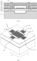
- FIG. 4 is a schematic diagram of a three-dimensional structure of a MEMS resonator according to this application.
- FIG. 4 is a sectional view obtained by cutting FIG. 21 along a dashed line.
- FIG. 5a to FIG. 51 are schematic diagrams of another structure of a MEMS resonator in different processing stages according to this application.
- FIG. 2a to FIG. 21 are referred to as Y sectional views
- FIG. 5a to FIG. 51 are referred to as X sectional views.
- FIG. 4 and FIG. 5a to FIG. 51 use numbers as the same those in FIG. 2a to FIG. 21. Therefore, for descriptions in FIG. 4 and FIG. 5a to FIG. 51, correspondingly refer to related descriptions in FIG. 2a to FIG. 21.
- the following describes a processing procedure of a functional electrode with reference to FIG. 4 , FIG. 5a to FIG. 51, and FIG. 1 .
- Step 101 Provide an SOI wafer including a substrate and a device silicon layer.
- an SOI wafer includes a substrate 201, a silicon oxide layer 202, and a device silicon layer 203.
- a piezoelectric layer 204 and an upper electrode layer 205 are included on the device silicon layer 203.
- a dielectric isolation layer 206 is deposited on the upper electrode layer 205 through atomic layer deposition.
- Step 102 Etch the device silicon layer to form a harmonic oscillator and a support beam.
- two functional electrodes 403 are formed by etching the device silicon layer 203.
- the two functional electrodes 403 are located on two sides of the harmonic oscillator 405.
- the functional electrode 403 and the harmonic oscillator 405 form a capacitor.
- a capacitor gap 404 exists between the functional electrode 403 and the harmonic oscillator 405. Openings exist in the functional electrode 403 and another part of the conducting layer 203, and are configured to implement electrical isolation.
- the dielectric isolation layer 206 is etched.
- an opening 1Y, an opening 2Y, and an opening 3Y are formed in the X sectional view.
- the opening 2Y and the opening 3Y are configured to form the capacitor gap 404.
- Apart between the opening 2Y and the opening 3Y is configured to form the harmonic oscillator 405.
- the device silicon layer 203 between the opening 1Y and the opening 2Y, and between the opening 1Y and the opening 3Y is configured to form the functional electrode 403.
- the opening 1Y is configured to isolate connection between the functional electrode 403 and another part of the device silicon layer 203.
- Step 103 Deposit a sacrificial layer on the device silicon layer. As shown in FIG. 5d , a sacrificial layer 207 is deposited on the device silicon layer 203.
- Step 104 Etch the sacrificial layer, and epitaxially grow or deposit a first barrier layer on the sacrificial layer, so that the harmonic oscillator is located in a cavity formed by the first barrier layer and the substrate.
- the sacrificial layer 207 is etched.
- an opening 6Y, an opening 7Y, an opening 8Y, and an opening 9Y are formed in the X sectional view.
- the opening 6Y and the opening 9Y are connected to the device silicon layer 203, to prepare for electrical connection to the functional electrode 403.
- the opening 7Y and the opening 8Y are connected to the dielectric isolation layer 206, and are used for subsequent generation of a first barrier layer or a second barrier layer.
- a distance between the opening 7Y and the opening 8Y is a width, in a Y-axis direction, of a cavity in which a subsequent harmonic oscillator is located.
- An area in which the sacrificial layer 207 between the opening 7Y and the opening 8Y is located is referred to as an area 10.
- the sacrificial layer 207 between the opening 6Y and the opening 7Y, and between the opening 8Y and the opening 9Y is referred to as a second electrical isolation structure.
- a first barrier layer 208 is formed on an etched sacrificial layer 207.
- Step 105 Etch breather holes on the first barrier layer. As shown in FIG. 5f , breather holes 11 are etched on the first barrier layer 208.
- Step 106 Inject hydrofluoric acid vapor through the breather holes to corrode the sacrificial layer, so that the harmonic oscillator is suspended, through the support beam, in the cavity.
- the breather holes 11 are connected to the sacrificial layer 207 in the area 10, after the hydrofluoric acid vapor is injected through the breather holes 11, the hydrofluoric acid vapor corrodes the sacrificial layer 207 in the area 10.
- Step 107 Epitaxially grow a second barrier layer on the first barrier layer to seal the breather holes.
- a second barrier layer 209 is epitaxially grown in a high-temperature vacuum environment to seal the breather holes 11.
- an electrical isolation groove is etched on the second barrier layer 209.
- an opening 12Y, an opening 13Y, an opening 14Y, and an opening 15Y are formed in the X sectional view.
- the opening 13Y and the opening 14Y are connected to the second electrical isolation structure.
- the second barrier layer 209 between the opening 12Y and the opening 13Y, and between the opening 14Y and the opening 15Y is referred to as a second conducting structure.
- the opening 12Y and the opening 15Y are configured to isolate connection between the second conducting structure and an edge part of the second barrier layer 209, to implement electrical isolation.
- a protective layer 210 is deposited on the second barrier layer 209 by using an LPCVD method.
- an electrical through-hole is etched on the protective layer 210.
- the electrical through-hole further includes an opening 16Y and an opening 16Y in the X sectional view.
- an electrical pad is formed by depositing metal on the electrical through-hole.
- the electrical pad includes functional electrode pads 401 formed on the opening 16Y and on the opening 17Y The functional electrode pad 401 is connected to the functional electrode 403 through the second conducting structure.
- a direct current bias voltage may be applied to the functional electrode 403 through the functional electrode pad 401.
- the harmonic oscillator 405 due to an electrostatic effect, the harmonic oscillator 405 generates an offset in a direction (Y direction) of the capacitor.
- a resonance frequency of the harmonic oscillator 405 changes. Therefore, in this application, the functional electrode 403 is disposed, to implement frequency adjustment of the harmonic oscillator
- FIG. 4 includes two symmetric functional electrodes 403. In actual application, only one functional electrode 403 may be included.
- the alternating current voltage is used as vibration excitation of the harmonic oscillator 405, which is briefly referred to as electrostatic excitation.
- a voltage applied to the upper electrode layer of the harmonic oscillator 405 may be used to perform detection on a vibration frequency of the harmonic oscillator 405, which is briefly referred to as piezoelectric detection. Through piezoelectric detection, it can be determined whether the vibration frequency of the harmonic oscillator meets an expected frequency. On the contrary, when a voltage applied to the upper electrode layer is used as vibration excitation of the harmonic oscillator 405, the voltage is briefly referred to as piezoelectric excitation.
- a direct current bias voltage applied to the functional electrode 403 may be used to perform detection on a vibration frequency of the harmonic oscillator 405, which briefly is referred to as electrostatic detection.
- the functional electrode 403 is disposed, to flexibly implement conversion between electrostatic excitation (piezoelectric detection) and piezoelectric excitation (electrostatic detection).
- FIG. 6 is a schematic diagram of electrical connections of a MEMS resonator according to this application.
- the MEMS resonator includes a lower electrode pad 211, an upper electrode pad 212, a functional electrode pad 401, a functional electrode 403, and a harmonic oscillator 405.
- a capacitor is formed between the harmonic oscillator 405 and the functional electrode 403.
- the functional electrode 403 is connected to the functional electrode pad 401.
- the lower electrode pad 211 is connected to a lower electrode layer of the harmonic oscillator 405, and the upper electrode pad 212 is connected to an upper electrode layer of the harmonic oscillator 405.
- a direction of a support beam is an X direction.
- a direction of an electrostatic force generated by the functional electrode 403 on the harmonic oscillator 405 is a Y direction.
- a direction of a capacitor formed between the functional electrode 403 and the harmonic oscillator is a Y direction.
- Two functional electrodes 403 include a first functional electrode and a second functional electrode.
- the first functional electrode and the harmonic oscillator 405 form a first capacitor
- the second functional electrode and the harmonic oscillator 405 form a second capacitor.
- the first capacitor and the second capacitor are distributed symmetric about the harmonic oscillator 405.
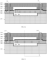
- FIG. 7 is a schematic diagram of a structure of a MEMS resonator according to this application.
- the MEMS resonator includes a substrate 701, a harmonic oscillator, and a barrier layer 702.
- the MEMS resonator includes a substrate 701, a barrier layer 702, a conducting layer 703, a dielectric isolation layer 704, a harmonic oscillator, a first electrical isolation structure 7061, and a first conducting structure 7051.
- the substrate 701 and the barrier layer 702 are combined to form a cavity.
- a junction between the substrate 701 and the barrier layer 702 includes the conducting layer 703.
- the dielectric isolation layer 704 is included between the conducting layer 703 and the barrier layer 702, and the dielectric isolation layer 704 is configured to isolate electrical connection between the conducting layer 703 and the barrier layer 702.
- the harmonic oscillator is suspended in the cavity.
- the harmonic oscillator includes an upper electrode layer 709, a piezoelectric layer 708, and a lower electrode layer 707.
- the lower electrode layer 707 is connected to the conducting layer 703 (not shown in the figure).
- the conducting layer 703 is connected to the first conducting structure 7051 that is outside the barrier layer 702.
- the first conducting structure 7051 may provide excitation for the harmonic oscillator, so that the harmonic oscillator vibrates in the cavity.
- the first electrical isolation structure 7061 is included between the first conducting structure 7051 and the barrier layer 702.
- the first electrical isolation structure 7061 is configured to isolate electrical connection between the first conducting structure 7051 and the barrier layer 702.
- the barrier layer 702 and the dielectric isolation layer 704 are configured to isolate the first electrical isolation structure 7051 from the cavity.
- the junction between the barrier layer 702 and the substrate 701 includes two parts: a left part and a right part.
- the left part includes the conducting layer 703.
- the right conducting layer includes an upper electrode layer, a piezoelectric layer, and a device silicon layer.
- a dielectric isolation layer is included between the right conducting layer and the barrier layer 702, and the dielectric isolation layer is configured to isolate electrical connection between the right conducting layer and the barrier layer 702.
- the harmonic oscillator is suspended in the cavity.
- the harmonic oscillator includes an upper electrode layer 709, a piezoelectric layer 708, and a lower electrode layer 707.
- the upper electrode layer 709 is connected to the right conducting layer.
- the right conducting layer is connected to a first conducting structure 7052 that is outside the barrier layer 702.
- a first electrical isolation structure 7062 is included between the first conducting structure 7052 and the barrier layer 702.
- the first electrical isolation structure 7062 is configured to isolate electrical connection between the first conducting structure 7052 and the barrier layer 702.
- the barrier layer 702 and the dielectric isolation layer are configured to isolate the first electrical isolation structure 7052 from the cavity.
- the substrate 701 refers to the substrate 201 in FIG. 2a to FIG. 21.
- the barrier layer 702 refer to the first barrier layer 208 and the second barrier layer 209 between an opening 11 and the opening 12 in FIG. 2i .
- the first conducting structure 7051 refer to the first barrier layer 208 and the second barrier layer 209 between the opening 12 and the opening 13 in FIG. 2i .
- the dielectric isolation layer 704 refer to the dielectric isolation layer 206 in FIG. 2a to FIG. 21.
- the first electrical isolation structure 7061 refer to the sacrificial layer 207 filled in the opening 11 in FIG. 2i .
- the upper electrode layer 709 refer to the upper electrode layer 205 in FIG. 5a to FIG. 51.
- the piezoelectric layer 708, refer to the piezoelectric layer 204 in FIG. 5a to FIG. 51.
- the lower electrode layer 707 refer to the device silicon layer 203 in the cavity in FIG. 5a to FIG. 51.
- the conducting layer may be the device silicon layer 203 at the junction between the barrier layer 702 and the substrate 701 in FIG. 2i to FIG. 21.
- the MEMS resonator further includes a functional electrode.
- FIG. 1 , FIG. 2a to FIG. 21, FIG. 4 , or FIG. 5a to FIG. 51 provide a plurality of MEMS resonator processing methods.
- the plurality of processing methods can be used to obtain the MEMS resonator provided in this application. Therefore, in actual application, there are more processing methods that can be used to obtain the MEMS resonator provided in this application.
- the processing methods provided in this application are merely particular examples among many processing methods. Therefore, the foregoing MEMS resonator processing method may be used as a reference for the MEMS resonator provided in this application, but shall not be used as a limiting condition.
- FIG. 8 is a schematic diagram of a structure of a clock device according to this application.
- the clock device includes a MEMS resonator 801 and a maintaining circuit 802.
- the maintaining circuit 802 provides closed-loop oscillation excitation for the MEMS resonator 801.
- the MEMS resonator 801 generates a clock signal through oscillation excitation.
- the MEMS resonator 801 refer to the foregoing MEMS resonator provided in this application.
- FIG. 9 is a schematic diagram of a structure of a terminal according to this application.
- the terminal may be a mobile phone, a computer, a base station, or the like.
- the terminal 903 includes a clock device 901 and a processor 902.
- the clock device 901 is configured to provide a clock signal for the processor 902.
- the processor 902 performs operation processing based on the clock signal.
- the processor 901 may be a central processing unit (central processing unit, CPU), a network processor (network processor, NP), or a combination of a CPU and an NP.
- the processor 901 may further include a hardware chip or another general purpose processor.
- the hardware chip may be an application-specific integrated circuit (application specific integrated circuit, ASIC), a programmable logic device (programmable logic device, PLD), or a combination thereof.
- the clock device 901 may be a MEMS clock device. Specifically, for the clock device 901, refer to the foregoing clock device provided in this application.
Landscapes
- Physics & Mathematics (AREA)
- Acoustics & Sound (AREA)
- Engineering & Computer Science (AREA)
- Manufacturing & Machinery (AREA)
- Piezo-Electric Or Mechanical Vibrators, Or Delay Or Filter Circuits (AREA)
- Micromachines (AREA)
- Oscillators With Electromechanical Resonators (AREA)
Applications Claiming Priority (2)
| Application Number | Priority Date | Filing Date | Title |
|---|---|---|---|
| CN202110285274.XA CN115118244A (zh) | 2021-03-17 | 2021-03-17 | Mems谐振器和mems谐振器的加工方法 |
| PCT/CN2022/080116 WO2022194018A1 (zh) | 2021-03-17 | 2022-03-10 | Mems谐振器和mems谐振器的加工方法 |
Publications (2)
| Publication Number | Publication Date |
|---|---|
| EP4290771A1 true EP4290771A1 (de) | 2023-12-13 |
| EP4290771A4 EP4290771A4 (de) | 2024-11-06 |
Family
ID=83321580
Family Applications (1)
| Application Number | Title | Priority Date | Filing Date |
|---|---|---|---|
| EP22770373.3A Pending EP4290771A4 (de) | 2021-03-17 | 2022-03-10 | Mems-resonator und verarbeitungsverfahren für mems-resonator |
Country Status (4)
| Country | Link |
|---|---|
| US (1) | US20240154598A1 (de) |
| EP (1) | EP4290771A4 (de) |
| CN (1) | CN115118244A (de) |
| WO (1) | WO2022194018A1 (de) |
Families Citing this family (2)
| Publication number | Priority date | Publication date | Assignee | Title |
|---|---|---|---|---|
| US12438516B2 (en) * | 2021-03-22 | 2025-10-07 | Agency For Science, Technology And Research | Resonator and method of forming the same |
| WO2022224972A1 (ja) * | 2021-04-19 | 2022-10-27 | 株式会社村田製作所 | 弾性波装置及び弾性波装置の製造方法 |
Family Cites Families (8)
| Publication number | Priority date | Publication date | Assignee | Title |
|---|---|---|---|---|
| US8766745B1 (en) * | 2007-07-25 | 2014-07-01 | Hrl Laboratories, Llc | Quartz-based disk resonator gyro with ultra-thin conductive outer electrodes and method of making same |
| JP2011004252A (ja) * | 2009-06-19 | 2011-01-06 | Sony Corp | 共振器およびその製造方法、発振器ならびに電子機器 |
| ITTO20111100A1 (it) * | 2011-11-30 | 2013-05-31 | St Microelectronics Srl | Dispositivo oscillatore e procedimento di fabbricazione dello stesso |
| JP2015211988A (ja) * | 2014-05-01 | 2015-11-26 | セイコーエプソン株式会社 | Mems構造体、電子機器および移動体 |
| US10291200B2 (en) * | 2014-07-02 | 2019-05-14 | The Royal Institution For The Advancement Of Learning / Mcgill University | Methods and devices for microelectromechanical resonators |
| JP6778407B2 (ja) * | 2017-06-20 | 2020-11-04 | 株式会社村田製作所 | 共振子及び共振装置 |
| CN110289823B (zh) * | 2019-05-31 | 2021-11-02 | 武汉大学 | 一种微机械谐振器 |
| CN111182429B (zh) * | 2020-01-03 | 2021-04-02 | 武汉大学 | 高填充率mems换能器 |
-
2021
- 2021-03-17 CN CN202110285274.XA patent/CN115118244A/zh active Pending
-
2022
- 2022-03-10 EP EP22770373.3A patent/EP4290771A4/de active Pending
- 2022-03-10 WO PCT/CN2022/080116 patent/WO2022194018A1/zh not_active Ceased
- 2022-03-10 US US18/550,628 patent/US20240154598A1/en active Pending
Also Published As
| Publication number | Publication date |
|---|---|
| CN115118244A (zh) | 2022-09-27 |
| WO2022194018A1 (zh) | 2022-09-22 |
| US20240154598A1 (en) | 2024-05-09 |
| EP4290771A4 (de) | 2024-11-06 |
Similar Documents
| Publication | Publication Date | Title |
|---|---|---|
| US9479139B2 (en) | Resonator device including electrode with buried temperature compensating layer | |
| US20190334503A1 (en) | Film bulk acoustic wave resonators and fabrication methods thereof | |
| US10432162B2 (en) | Acoustic resonator including monolithic piezoelectric layer having opposite polarities | |
| US20130049545A1 (en) | Resonator device including electrodes with buried temperature compensating layers | |
| US20240154598A1 (en) | Mems resonator and mems resonator processing method | |
| US20140292149A1 (en) | Temperature compensated acoustic resonator device | |
| US8519806B2 (en) | Bulk-mode resonator having at least partially filled open cavities | |
| US12531538B2 (en) | Piezoelectric microelectromechanical resonator device and corresponding manufacturing process | |
| US12034431B2 (en) | Piezoelectric MEMS resonators based on porous silicon technologies | |
| US11664783B2 (en) | Resonator and semiconductor device | |
| CN113285687A (zh) | 温度补偿型薄膜体声波谐振器及其形成方法、电子设备 | |
| WO2022143286A1 (zh) | 单晶体声波谐振器、滤波器及电子设备 | |
| WO2019228750A1 (en) | Method of manufacturing a bulk acoustic wave resonator and bulk acoustic wave resonator device | |
| CN113364423B (zh) | 压电mems谐振器及其形成方法、电子设备 | |
| CN212163290U (zh) | 一种钪掺杂氮化铝兰姆波谐振器 | |
| US12308821B2 (en) | Resonator and resonance device | |
| US12107564B2 (en) | Resonator and resonance device including the same | |
| US11939215B2 (en) | Microelectromechanical structure including a functional element situated in a cavity of the microelectromechanical structure | |
| WO2022206497A1 (zh) | Mems谐振器及其加工方法,时钟器件 | |
| WO2022226914A1 (zh) | 具有梁结构的压电mems硅谐振器及其形成方法、电子设备 | |
| US12445104B2 (en) | FBAR filter with trap rich layer | |
| US20240128948A1 (en) | Resonance device and method for manufacturing same | |
| JP2006238115A (ja) | 圧電振動子の周波数調整方法 | |
| CN119788014A (zh) | 体声波谐振器制备方法、体声波谐振器及滤波器 | |
| WO2023162301A1 (ja) | 共振子、共振装置、及び共振子製造方法 |
Legal Events
| Date | Code | Title | Description |
|---|---|---|---|
| STAA | Information on the status of an ep patent application or granted ep patent |
Free format text: STATUS: THE INTERNATIONAL PUBLICATION HAS BEEN MADE |
|
| PUAI | Public reference made under article 153(3) epc to a published international application that has entered the european phase |
Free format text: ORIGINAL CODE: 0009012 |
|
| STAA | Information on the status of an ep patent application or granted ep patent |
Free format text: STATUS: REQUEST FOR EXAMINATION WAS MADE |
|
| 17P | Request for examination filed |
Effective date: 20230905 |
|
| AK | Designated contracting states |
Kind code of ref document: A1 Designated state(s): AL AT BE BG CH CY CZ DE DK EE ES FI FR GB GR HR HU IE IS IT LI LT LU LV MC MK MT NL NO PL PT RO RS SE SI SK SM TR |
|
| DAV | Request for validation of the european patent (deleted) | ||
| DAX | Request for extension of the european patent (deleted) | ||
| RIC1 | Information provided on ipc code assigned before grant |
Ipc: H03H 3/02 20060101ALI20240712BHEP Ipc: H03H 9/05 20060101ALI20240712BHEP Ipc: H03H 9/54 20060101ALI20240712BHEP Ipc: H03H 9/46 20060101ALI20240712BHEP Ipc: H03H 9/10 20060101ALI20240712BHEP Ipc: H03H 9/02 20060101ALI20240712BHEP Ipc: H03H 3/007 20060101AFI20240712BHEP |
|
| A4 | Supplementary search report drawn up and despatched |
Effective date: 20241009 |
|
| RIC1 | Information provided on ipc code assigned before grant |
Ipc: H03H 3/02 20060101ALI20241003BHEP Ipc: H03H 9/05 20060101ALI20241003BHEP Ipc: H03H 9/54 20060101ALI20241003BHEP Ipc: H03H 9/46 20060101ALI20241003BHEP Ipc: H03H 9/10 20060101ALI20241003BHEP Ipc: H03H 9/02 20060101ALI20241003BHEP Ipc: H03H 3/007 20060101AFI20241003BHEP |