EP4290341A2 - Stift und berührungseingabesystem oder -steuergerät - Google Patents
Stift und berührungseingabesystem oder -steuergerät Download PDFInfo
- Publication number
- EP4290341A2 EP4290341A2 EP23177774.9A EP23177774A EP4290341A2 EP 4290341 A2 EP4290341 A2 EP 4290341A2 EP 23177774 A EP23177774 A EP 23177774A EP 4290341 A2 EP4290341 A2 EP 4290341A2
- Authority
- EP
- European Patent Office
- Prior art keywords
- patterns
- pattern
- pen
- sensing
- disposed
- Prior art date
- Legal status (The legal status is an assumption and is not a legal conclusion. Google has not performed a legal analysis and makes no representation as to the accuracy of the status listed.)
- Pending
Links
Images













Classifications
-
- G—PHYSICS
- G06—COMPUTING OR CALCULATING; COUNTING
- G06F—ELECTRIC DIGITAL DATA PROCESSING
- G06F3/00—Input arrangements for transferring data to be processed into a form capable of being handled by the computer; Output arrangements for transferring data from processing unit to output unit, e.g. interface arrangements
- G06F3/01—Input arrangements or combined input and output arrangements for interaction between user and computer
- G06F3/03—Arrangements for converting the position or the displacement of a member into a coded form
- G06F3/033—Pointing devices displaced or positioned by the user, e.g. mice, trackballs, pens or joysticks; Accessories therefor
- G06F3/0354—Pointing devices displaced or positioned by the user, e.g. mice, trackballs, pens or joysticks; Accessories therefor with detection of two-dimensional [2D] relative movements between the device, or an operating part thereof, and a plane or surface, e.g. 2D mice, trackballs, pens or pucks
- G06F3/03545—Pens or stylus
-
- G—PHYSICS
- G06—COMPUTING OR CALCULATING; COUNTING
- G06F—ELECTRIC DIGITAL DATA PROCESSING
- G06F3/00—Input arrangements for transferring data to be processed into a form capable of being handled by the computer; Output arrangements for transferring data from processing unit to output unit, e.g. interface arrangements
- G06F3/01—Input arrangements or combined input and output arrangements for interaction between user and computer
- G06F3/03—Arrangements for converting the position or the displacement of a member into a coded form
- G06F3/041—Digitisers, e.g. for touch screens or touch pads, characterised by the transducing means
- G06F3/0416—Control or interface arrangements specially adapted for digitisers
- G06F3/04162—Control or interface arrangements specially adapted for digitisers for exchanging data with external devices, e.g. smart pens, via the digitiser sensing hardware
-
- G—PHYSICS
- G06—COMPUTING OR CALCULATING; COUNTING
- G06F—ELECTRIC DIGITAL DATA PROCESSING
- G06F3/00—Input arrangements for transferring data to be processed into a form capable of being handled by the computer; Output arrangements for transferring data from processing unit to output unit, e.g. interface arrangements
- G06F3/01—Input arrangements or combined input and output arrangements for interaction between user and computer
- G06F3/03—Arrangements for converting the position or the displacement of a member into a coded form
- G06F3/041—Digitisers, e.g. for touch screens or touch pads, characterised by the transducing means
- G06F3/044—Digitisers, e.g. for touch screens or touch pads, characterised by the transducing means by capacitive means
- G06F3/0446—Digitisers, e.g. for touch screens or touch pads, characterised by the transducing means by capacitive means using a grid-like structure of electrodes in at least two directions, e.g. using row and column electrodes
-
- G—PHYSICS
- G06—COMPUTING OR CALCULATING; COUNTING
- G06F—ELECTRIC DIGITAL DATA PROCESSING
- G06F3/00—Input arrangements for transferring data to be processed into a form capable of being handled by the computer; Output arrangements for transferring data from processing unit to output unit, e.g. interface arrangements
- G06F3/01—Input arrangements or combined input and output arrangements for interaction between user and computer
- G06F3/03—Arrangements for converting the position or the displacement of a member into a coded form
- G06F3/041—Digitisers, e.g. for touch screens or touch pads, characterised by the transducing means
- G06F3/046—Digitisers, e.g. for touch screens or touch pads, characterised by the transducing means by electromagnetic means
-
- G—PHYSICS
- G06—COMPUTING OR CALCULATING; COUNTING
- G06F—ELECTRIC DIGITAL DATA PROCESSING
- G06F2203/00—Indexing scheme relating to G06F3/00 - G06F3/048
- G06F2203/041—Indexing scheme relating to G06F3/041 - G06F3/045
- G06F2203/04111—Cross over in capacitive digitiser, i.e. details of structures for connecting electrodes of the sensing pattern where the connections cross each other, e.g. bridge structures comprising an insulating layer, or vias through substrate
-
- G—PHYSICS
- G06—COMPUTING OR CALCULATING; COUNTING
- G06F—ELECTRIC DIGITAL DATA PROCESSING
- G06F2203/00—Indexing scheme relating to G06F3/00 - G06F3/048
- G06F2203/041—Indexing scheme relating to G06F3/041 - G06F3/045
- G06F2203/04112—Electrode mesh in capacitive digitiser: electrode for touch sensing is formed of a mesh of very fine, normally metallic, interconnected lines that are almost invisible to see. This provides a quite large but transparent electrode surface, without need for ITO or similar transparent conductive material
Definitions
- the present disclosure relates to a pen and a controller, and more particularly, to a touch input system including a sensor unit and interacting with a stylus pen and a controller for controlling a device.
- a touch sensor is provided in various touch input devices such as mobile phones, smart phones, laptop computers, digital broadcasting terminals, personal digital assistants (PDA), portable multimedia players (PMP), navigation units, slate PCs, tablet PCs, ultrabooks, and wearable devices.
- PDA personal digital assistants
- PMP portable multimedia players
- navigation units slate PCs, tablet PCs, ultrabooks, and wearable devices.
- the touch sensor in the touch input device may be disposed on a display panel that displays an image or a portion of the touch input device. As a user touches a touch sensor to interact with the touch input device, the touch input device may provide an intuitive user interface to the user.
- the user may use a stylus pen for a precise touch input.
- the stylus pen may be classified into an active stylus pen and a passive stylus pen depending on whether a battery and an electronic component are provided therein.
- the active stylus pen has an excellent basic performance and provides additional functions (pen pressure, hovering, and buttons) in comparison with the passive stylus pen, the active stylus pen is expensive and uses a rechargeable battery as power. Thus, not many users substantially use the active stylus pen except for some advanced users.
- the passive stylus pen is inexpensive and does not require a battery in comparison with the active stylus pen, the passive stylus pen is difficult to recognize a precise touch in comparison with the active stylus pen.
- technologies of an electro magnetic resonance (EMR) method that is an inductive resonance method and a capacitive resonance method are proposed to realize a passive stylus pen capable of recognizing a precise touch.
- the EMR method is excellent in writing and drawing quality that is a key function of the stylus pen, the EMR method has a great thickness and requires more costs because a separate EMR sensor panel and a separate EMR driving IC are necessarily added in addition to a capacitance touch panel.
- the capacitive resonance method uses a general capacitance touch sensor and a general touch controller IC to increase a performance of the IC and support a pen touch without additional costs.
- a resonance signal is required to have a large amplitude to more accurately distinguish a touch caused by the stylus pen.
- a driving signal transmitted to the stylus pen needs to have the almost same resonance frequency as that of the resonance circuit contained in the stylus pen.
- the resonance frequency is the same as a frequency of the driving signal, signal transmission is difficult because of extremely great attenuation of the signal transmission.
- no companies have succeeded in mass production yet because a sufficient output signal is not produced.
- a feature of how to design structures of the internal resonance circuit and the pen is a key factor to manufacture an EMR or capacitive resonance stylus pen capable of producing a maximum output signal.
- the present disclosure provides a pen including a stylus pen producing sufficient output signals, a touch input system interacting with a stylus pen, and a controller for controlling a device.
- the present disclosure also provides a pen including a multifunctional touch input device capable of driving a stylus pen and detecting a position of the stylus pen and a controller for controlling a touch input system.
- the present disclosure also provides a pen including a touch input device capable of solving a limitation in which an output voltage of a sensing circuit unit is varied depending on positions of a stylus pen and a controller for controlling a touch input system.
- the problem to be solved in the present invention is not limited to the above-described problems.
- An embodiment of the present invention provides a pen and touch input system including: a touch input device including a sensor unit and a control unit configured to control the sensor unit; and a stylus pen configured to interact with the touch input device.
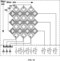
- the sensor unit includes: a first pattern extending in a first direction; a second pattern disposed adjacent to the first pattern and extending in the first direction; a third pattern extending in a second direction different from the first direction; and a fourth pattern disposed adjacent to the third pattern and extending in the second direction.
- a plurality of first patterns and a plurality of second patterns are arranged in the second direction, and a plurality of third patterns and a plurality of fourth patterns are arranged in the first direction, first ends of the plurality of first and third patterns are electrically connected to the control unit, and second ends thereof are electrically opened, and second ends of the plurality of second patterns are electrically connected to each other, and second ends of the plurality of fourth patterns are electrically connected to each other.
- the stylus pen includes: a body unit; a tip exposed to the outside in the body unit; an inductor unit including a ferrite core disposed in the body unit and a coil wound in multiple layers around at least a portion of the ferrite core; and a capacitor unit disposed in the body unit and electrically connected to the inductor unit to form a resonance circuit.
- the control unit drives the stylus pen by using at least one driving pattern among the plurality of first to fourth patterns.
- a pen and touch input system including: a touch input device including a sensor unit and a control unit configured to control the sensor unit; and a stylus pen configured to interact with the touch input device.
- the sensor unit includes: a first pattern extending in a first direction; a second pattern disposed adjacent to the first pattern and extending in the first direction; a third pattern extending in a second direction different from the first direction; and a fourth pattern disposed adjacent to the third pattern and extending in the second direction.
- a plurality of first patterns and a plurality of second patterns are arranged in the second direction, and a plurality of third patterns and a plurality of fourth patterns are arranged in the first direction, first ends of the plurality of first and third patterns are electrically connected to the control unit, and second ends thereof are electrically opened, and second ends of the plurality of second patterns are electrically connected to each other, and second ends of the plurality of fourth patterns are electrically connected to each other.
- the stylus pen includes: a body unit; a tip exposed to the outside in the body unit; an inductor unit including a ferrite core disposed in the body unit and a coil wound in multiple layers around at least a portion of the ferrite core; and a capacitor unit disposed in the body unit and electrically connected to the inductor unit to form a resonance circuit.
- the control unit senses the stylus pen by using at least one sensing pattern among the plurality of first to fourth patterns.
- a pen and touch input system including: a touch input device including a sensor unit and a control unit configured to control the sensor unit; and a stylus pen configured to interact with the touch input device.
- the sensor unit includes: a first pattern including first-a patterns and first-b patterns that are alternately arranged in a first direction; a second pattern disposed adjacent to the first pattern; a third pattern extending in a second direction different from the first direction; and a fourth pattern disposed adjacent to the third pattern and extending in the second direction.
- first-a patterns are electrically connected to each other
- first-b patterns are electrically connected to each other
- a plurality of first patterns and a plurality of second patterns are arranged in the second direction
- a plurality of third patterns and a plurality of fourth patterns are arranged in the first direction
- first ends of the plurality of first and third patterns are electrically connected to the control unit, and second ends thereof are electrically opened
- second ends of the plurality of second patterns are electrically connected to each other
- second ends of the plurality of fourth patterns are electrically connected to each other.
- the stylus pen includes: a body unit; a tip exposed to the outside in the body unit; an inductor unit including a ferrite core disposed in the body unit and a coil wound in multiple layers around at least a portion of the ferrite core; and a capacitor unit disposed in the body unit and electrically connected to the inductor unit to form a resonance circuit.
- the control unit drives the stylus pen by using at least one driving pattern among the plurality of first to fourth patterns.
- a pen and touch input system including: a touch input device including a sensor unit and a control unit configured to control the sensor unit; and a stylus pen configured to interact with the touch input device.
- the sensor unit includes: a first pattern including first-a patterns and first-b patterns that are alternately arranged in a first direction; a second pattern disposed adjacent to the first pattern; a third pattern extending in a second direction different from the first direction; and a fourth pattern disposed adjacent to the third pattern and extending in the second direction.
- first-a patterns are electrically connected to each other
- first-b patterns are electrically connected to each other
- a plurality of first patterns and a plurality of second patterns are arranged in the second direction
- a plurality of third patterns and a plurality of fourth patterns are arranged in the first direction
- first ends of the plurality of first and third patterns are electrically connected to the control unit, and second ends thereof are electrically opened
- second ends of the plurality of second patterns are electrically connected to each other
- second ends of the plurality of fourth patterns are electrically connected to each other.
- the stylus pen includes: a body unit; a tip exposed to the outside in the body unit; an inductor unit including a ferrite core disposed in the body unit and a coil wound in multiple layers around at least a portion of the ferrite core; and a capacitor unit disposed in the body unit and electrically connected to the inductor unit to form a resonance circuit.
- the control unit drives the stylus pen by using at least one driving pattern among the plurality of first to fourth patterns.
- a pen and touch input system including: a touch input device including a sensor unit and a control unit configured to control the sensor unit; and a stylus pen configured to interact with the touch input device.
- the sensor unit includes: a plurality of first patterns arranged in a first direction and a second direction different from the first direction and each having an opening; a plurality of second patterns disposed in the openings of the first patterns; a plurality of third patterns disposed on the same layer as the plurality of first patterns and each extending in the second direction and each having an opening; and a plurality of fourth patterns disposed in the openings of the plurality of third patterns, respectively, and each extending in the second direction.
- the first patterns arranged in the first direction among the plurality of first patterns are electrically connected to each other through a conductive bridge, among the first patterns arranged in the first direction, the first pattern disposed on a first end is connected to the control unit, and the first pattern disposed on a second end is electrically opened, the second patterns arranged in the first direction among the plurality of second patterns are electrically connected to each other through a conductive bridge, the second pattern disposed on a second end among the second patterns arranged in the first direction are electrically connected to other second patterns arranged in the second direction, first ends of the plurality of third patterns are electrically connected to the control unit, and second ends thereof are electrically opened, and second ends of the plurality of fourth patterns are electrically connected to each other.
- the stylus pen includes: a body unit; a tip exposed to the outside in the body unit; an inductor unit including a ferrite core disposed in the body unit and a coil wound in multiple layers around at least a portion of the ferrite core; and a capacitor unit disposed in the body unit and electrically connected to the inductor unit to form a resonance circuit.
- the control unit drives the stylus pen by using at least one driving pattern among the plurality of first to fourth patterns.
- a pen and touch input system including: a touch input device including a sensor unit and a control unit configured to control the sensor unit; and a stylus pen configured to interact with the touch input device.
- the sensor unit includes: a plurality of first patterns arranged in a first direction and a second direction different from the first direction and each having an opening; a plurality of second patterns disposed in the openings of the plurality of first patterns; a plurality of third patterns arranged on the same layer as the plurality of first patterns, each extending in the second direction, and each having an opening; and a plurality of fourth patterns arranged in the openings of the plurality of third patterns, respectively, and each extending in the second direction.
- the first patterns arranged in the first direction among the plurality of first patterns are electrically connected to each other through a conductive bridge, among the first patterns arranged in the first direction, the first pattern disposed on a first end is connected to the control unit, and the first pattern disposed on a second end is electrically opened, the second pattern arranged in the first direction among the plurality of second patterns are electrically connected through a conductive bridge, among the second patterns arranged in the first direction, the second pattern disposed on a second end is connected to other second patterns arranged in the second direction, first ends of the plurality of third patterns are electrically connected to the control unit, and second ends thereof are electrically opened, and second ends of the plurality of fourth patterns are electrically connected to each other.
- the stylus pen includes: a body unit; a tip exposed to the outside in the body unit; an inductor unit including a ferrite core disposed in the body unit and a coil wound in multiple layers around at least a portion of the ferrite core; and a capacitor unit disposed in the body unit and electrically connected to the inductor unit to form a resonance circuit.
- the control unit senses the stylus pen by using at least one sensing pattern among the plurality of first to fourth patterns.
- a pen and touch input system including: a touch input device including a sensor unit and a control unit configured to control the sensor unit; and a stylus pen configured to interact with the touch input device.
- the sensor unit includes: a plurality of first patterns each extending in a first direction; and a plurality of second patterns each extending in a second direction different from the first direction.
- each of the first patterns includes a plurality of first-1 patterns, a plurality of first-2 patterns, and a connection pattern configured to connect at least two first-1 patterns to each other among the plurality of first-1 patterns, and the plurality of first-2 patterns are electrically connected to each other.
- each of the second patterns includes a plurality of second-1 patterns, a plurality of second-2 patterns, the plurality of second-1 patterns are electrically connected to each other, and the plurality of second-2 patterns are electrically connected to each other.
- the first-1 patterns disposed on a second end among the plurality of first-1 patterns are electrically opened, and the first-2 patterns disposed on the second end among the plurality of first-2 patterns are electrically connected to each other.
- the second-1 patterns disposed on the second end among the plurality of second-1 patterns are electrically opened, and the second-2 patterns disposed on the second end among the plurality of second-2 patterns are electrically connected to each other.
- the stylus pen includes: a body unit; a tip exposed to the outside in the body unit; an inductor unit including a ferrite core disposed in the body unit and a coil wound in multiple layers around at least a portion of the ferrite core; and a capacitor unit disposed in the body unit and electrically connected to the inductor unit to form a resonance circuit.
- the control unit drives the stylus pen by using at least one driving pattern among the first-1 pattern, the first-2 pattern, the second-1 pattern, and the second-2 pattern.
- a pen and touch input system including: a touch input device including a sensor unit and a control unit configured to control the sensor unit; and a stylus pen configured to interact with the touch input device.
- the sensor unit includes: a plurality of first patterns each extending in a first direction; and a plurality of second patterns each extending in a second direction different from the first direction.
- each of the first patterns includes a plurality of first-1 patterns, a plurality of first-2 patterns, and a connection pattern configured to connect at least two first-1 patterns to each other among the plurality of first-1 patterns, and the plurality of first-2 patterns are electrically connected to each other.
- each of the second patterns includes a plurality of second-1 patterns, a plurality of second-2 patterns, the plurality of second-1 patterns are electrically connected to each other, and the plurality of second-2 patterns are electrically connected to each other.
- the first-1 patterns disposed on a second end among the plurality of first-1 patterns are electrically opened, and the first-2 patterns disposed on the second end among the plurality of first-2 patterns are electrically connected to each other.
- the second-1 patterns disposed on the second end among the plurality of second-1 patterns are electrically opened, and the second-2 patterns disposed on the second end among the plurality of second-2 patterns are electrically connected to each other.
- the stylus pen includes: a body unit; a tip exposed to the outside in the body unit; an inductor unit including a ferrite core disposed in the body unit and a coil wound in multiple layers around at least a portion of the ferrite core; and a capacitor unit disposed in the body unit and electrically connected to the inductor unit to form a resonance circuit.
- the control unit senses the stylus pen by using at least one sensing pattern among the first-1 pattern, the first-2 pattern, the second-1 pattern, and the second-2 pattern.
- the ferrite core may have a dielectric constant of 1000 or less
- the coil may be formed such that adjacent winding layers are alternately wound, and the coil is a wire that surrounds two or more insulating wires.
- the coil may be formed such that adjacent winding layers are wound in an inclined zigzag pattern.
- the ferrite core may include nickel.
- the coil may be a litz wire.
- the pen and touch input system may further include a bobbin that surrounds at least a portion of the ferrite core, and the coil may be wound around at least a portion of the bobbin.
- the inductor unit may be formed such that two or more inductor units are connected in series.
- the pen and touch input system may further include a conductive blocking member disposed on at least a portion of the inductor unit.
- the blocking member may include one slit configured to block generation of an eddy current, both ends of the blocking member may be spaced apart from each other in the first direction by the one slit, and the first direction may be a direction in which the eddy current is formed.
- any one of the first to fourth patterns may include a plurality of diamond patterns and a connection pattern configured to connect two adjacent diamond patterns among the plurality of diamond patterns.
- the first-1 pattern may have a diamond shape
- the connection pattern may connect two adjacent first-1 patterns.
- the first-1 pattern or the first-2 pattern may have a diamond shape, and the first pattern may further include a connection pattern configured to connect two adjacent first-2 patterns.
- the first pattern or the third pattern may have an opening
- the second pattern or the fourth pattern may be disposed in the opening of the first pattern or the third pattern, respectively.
- first-1 pattern or the second-1 pattern may have an opening
- first-2 pattern or the second-2 pattern may be disposed in the opening of the first-1 pattern or the second-1 pattern, respectively.
- the first pattern or the third pattern may surround the second pattern or the fourth pattern, respectively.
- first-1 pattern or the second-1 pattern may surround the first-2 pattern or the second-2 pattern, respectively.
- first pattern and the second may be disposed on the same layer, or the third pattern and the fourth pattern may be disposed on the same layer.
- first pattern and the second pattern may be disposed on the same layer.
- At least a portion of the first pattern and at least a portion of the second pattern may be disposed on a first layer, and at least a portion of the second pattern and at least a portion of the fourth pattern may be disposed on a second layer.
- At least a portion of the first-1 pattern, at least a portion of the first-2 pattern, and at least a portion of the connection pattern may be disposed on a first layer, and at least a portion of the second-1 pattern and at least a portion of the second-2 pattern may be disposed on a second layer.
- the plurality of first-2 pattern, the second-1 pattern, or the plurality of second-2 pattern may be electrically connected to each other by a structure different from that of the connection pattern configured to connect the first-1 patterns to each other.
- the plurality of first-2 pattern, the plurality of second-1 pattern, or the plurality of second-2 pattern may be electrically connected to each other through a bridge and a via.
- the pen and touch input system may further include a second connection pattern configured to connect at least two adjacent first-2 patterns among the plurality of first-2 patterns, and the second-1 pattern or the plurality of second-2 patterns may be electrically connected to each other by a structure different from that of the connection pattern configured to connect the first-1 patterns to each other.
- the plurality of second-1 patterns or the plurality of second-2 patterns may be electrically connected to each other through a bridge and a via.
- second ends of the plurality of second and fourth patterns may be electrically connected to each other through a via.
- first-2 patterns disposed on the second end among the plurality of first-2 patterns may be electrically connected through a via.
- the second-2 patterns disposed on the second end among the plurality of second-2 patterns may be electrically connected to each other through a via.
- the first-1 patterns disposed on the second end among the plurality of first-1 patterns may have a shape opened in the first direction, and the first-2 patterns disposed on the second end among the plurality of first-2 patterns may be electrically connected through the connection pattern.
- the second-1 patterns disposed on the second end among the plurality of second-1 patterns may have a shape opened in the second direction, and the second-2 patterns disposed on the second end among the plurality of second-2 patterns may be electrically connected through the connection pattern.
- a first end of the first-a patterns may be electrically opened
- a second end of the first-a patterns may be electrically connected to the control unit
- a first end of the first-b patterns may be electrically connected to the control unit
- a second end of the first-b patterns may be electrically opened.
- control unit may apply a driving signal for touch sensing to at least one first pattern among the plurality of first patterns and receive a sensing signal received from at least one third pattern among the plurality of third patterns.
- control unit may include a recording medium in which a program is recorded for executing: a process of applying a driving signal for touch sensing to at least one first pattern among the plurality of first patterns; and a process of receiving a sensing signal received from at least one third pattern among the plurality of third patterns.
- control unit may: apply a driving signal for touch sensing to at least one first-1 pattern among the plurality of first-1 patterns and receive a sensing signal received from at least one second-1 pattern among the plurality of second-1 patterns; or apply a driving signal for touch sensing to at least one second-1 pattern among the plurality of second-1 patterns and receive a sensing signal received from at least one first-1 pattern among the plurality of first-1 patterns.
- control unit may include a recording medium in which a program is recorded for executing: a process of applying a driving signal for touch sensing to at least one first-1 pattern among the plurality of first-1 patterns and a process of receiving a sensing signal received from at least one second-1 pattern among the plurality of second-1 patterns; or a process of applying a driving signal for touch sensing to at least one second-1 pattern among the plurality of second-1 patterns and a process of receiving a sensing signal received from at least one first-1 pattern among the plurality of first-1 patterns.
- control unit may further include: a plurality of driving circuit units for touch sensing; and a plurality of sensing circuit units for touch sensing, and the control unit may control to: apply a driving signal for touch sensing to at least one driving pattern among the plurality of first or third patterns through the plurality of driving circuit units for touch sensing, and receive a sensing signal for touch sensing received from at least one sensing pattern among the plurality of first or third patterns through the plurality of sensing circuit units for touch sensing.
- control unit may further include: a plurality of driving circuit units for touch sensing; and a plurality of sensing circuit units for touch sensing, and the control unit may control to: apply a driving signal for touch sensing to at least one driving pattern among the plurality of first-1 or second-1 patterns through the plurality of driving circuit units for touch sensing, and receive a sensing signal for touch sensing received from at least one sensing pattern among the plurality of first-1 or second-1 patterns through the plurality of sensing circuit units for touch sensing.
- control unit may allow: a driving signal to be outputted to at least one driving pattern among the plurality of driving patterns, and a driving signal opposite to the above-described driving signal to be outputted to at least another driving pattern among the plurality of driving patterns.
- control unit may include a recording medium in which a program is recorded for executing: a process of outputting a driving signal to at least one driving pattern among the plurality of driving patterns, and a process of outputting a driving signal opposite to the above-described driving signal to at least another driving pattern among the plurality of driving patterns.
- control unit may include a plurality of driving circuit units for pen driving, and the control unit may control to: apply a driving signal to at least one driving pattern through at least one driving circuit unit for pen driving through at least one driving circuit unit for pen driving among the plurality of driving circuit for pen driving; and apply a driving signal opposite to the above-described driving signal to at least another driving pattern through at least another driving circuit unit for pen driving among the plurality of driving circuit units for pen driving.
- control unit may control to sense the pen based on an output value from at least one sensing pattern among the plurality of sensing patterns and an output value from at least one sensing pattern among other sensing patterns different from the plurality of sensing patterns.
- control unit may include a recording medium in which a program is recorded for executing: a process of sensing the pen based on an output value from at least one sensing pattern among the plurality of sensing patterns and an output value from at least one sensing pattern among other sensing patterns different from the plurality of sensing patterns.
- control unit may include a plurality of sensing circuit units for pen sensing, and the control unit may control to sense the pen based on an outer value from at least one sensing pattern among the plurality of sensing patterns, which is sensed through at least one sensing circuit unit for pen sensing among the plurality of sensing circuit units for pen sensing and an output value from at least one sensing pattern among other sensing patterns different from the plurality of sensing patterns which is sensed through at least one sensing circuit unit for pen sensing among the plurality of sensing circuit units for pen sensing.
- the sensing circuit unit for pen sensing may be used for touch sensing.
- the pen and touch input system may further include a capacitor connected to a pattern of the second end among the plurality of second patterns or the plurality of fourth patterns.
- the pen and touch input system may further include a capacitor connected to a pattern of the second end among the plurality of first-2 patterns or the plurality of second-2 patterns.
- the second pattern may be a bar pattern disposed in the first pattern and extending in the first direction
- the fourth pattern may be a bar pattern disposed in the third pattern and extending in the second direction
- the pen and touch input system may further include: a plurality of fifth patterns disposed between the plurality of first patterns, having a shape corresponding to and overlapping a main pattern part of the third pattern, and electrically connected to the fourth pattern; a capacitor connected to a pattern of the second end among the plurality of fifth patterns; a plurality of sixth patterns disposed between the plurality of third patterns, having a shape corresponding to and overlapping a main pattern part of the first pattern, and electrically connected to the second pattern; and a capacitor connected to the pattern of the second end among the plurality of sixth patterns.
- the pen and touch input system may further include at least one trace directly connected to a portion at which the patterns disposed on the second end are electrically connected to each other and disposed outside an active area of the touch input device.
- An embodiment of the present invention provides a controller configured to control a touch input device including a sensor unit and interacting with a stylus pen.
- the sensor unit includes: a first pattern extending in a first direction; a second pattern disposed adjacent to the first pattern and extending in the first direction; a third pattern extending in a second direction different from the first direction; and a fourth pattern disposed adjacent to the third pattern and extending in the second direction.
- a plurality of first patterns and a plurality of second patterns are arranged in the second direction, and a plurality of third patterns and a plurality of fourth patterns are arranged in the first direction, first ends of the plurality of first and third patterns are electrically connected to the controller, and second ends thereof are electrically opened, and second ends of the plurality of second patterns are electrically connected to each other, and second ends of the plurality of fourth patterns are electrically connected to each other.
- the stylus pen includes: a body unit; a tip exposed to the outside in the body unit; an inductor unit including a ferrite core disposed in the body unit and a coil wound in multiple layers around at least a portion of the ferrite core; and a capacitor unit disposed in the body unit and electrically connected to the inductor unit to form a resonance circuit.
- the controller drives the stylus pen by using at least one driving pattern among the plurality of first to fourth patterns.
- the present invention provides a controller configured to control a touch input device including a sensor unit and interacting with a stylus pen.
- the sensor unit includes: a first pattern extending in a first direction; a second pattern disposed adjacent to the first pattern and extending in the first direction; a third pattern extending in a second direction different from the first direction; and a fourth pattern disposed adjacent to the third pattern and extending in the second direction.
- a plurality of first patterns and a plurality of second patterns are arranged in the second direction, and a plurality of third patterns and a plurality of fourth patterns are arranged in the first direction, first ends of the plurality of first and third patterns are electrically connected to the controller, and second ends thereof are electrically opened, and second ends of the plurality of second patterns are electrically connected to each other, and second ends of the plurality of fourth patterns are electrically connected to each other.
- the stylus pen includes: a body unit; a tip exposed to the outside in the body unit; an inductor unit including a ferrite core disposed in the body unit and a coil wound in multiple layers around at least a portion of the ferrite core; and a capacitor unit disposed in the body unit and electrically connected to the inductor unit to form a resonance circuit. Also, the controller senses the stylus pen by using at least one sensing pattern among the plurality of first to fourth patterns.
- the present invention provides a controller configured to control a touch input device including a sensor unit and interacting with a stylus pen.
- the sensor unit includes: a first pattern including first-a patterns and first-b patterns that are alternately arranged in a first direction; a second pattern disposed adjacent to the first pattern; a third pattern extending in a second direction different from the first direction; and a fourth pattern disposed adjacent to the third pattern and extending in the second direction.
- first-a patterns are electrically connected to each other
- first-b patterns are electrically connected to each other
- a plurality of first patterns and a plurality of second patterns are arranged in the second direction
- a plurality of third patterns and a plurality of fourth patterns are arranged in the first direction
- first ends of the plurality of first and third patterns are electrically connected to the controller, and second ends thereof are electrically opened
- second ends of the plurality of second patterns are electrically connected to each other
- second ends of the plurality of fourth patterns are electrically connected to each other.
- the stylus pen includes: a body unit; a tip exposed to the outside in the body unit; an inductor unit including a ferrite core disposed in the body unit and a coil wound in multiple layers around at least a portion of the ferrite core; and a capacitor unit disposed in the body unit and electrically connected to the inductor unit to form a resonance circuit.
- the controller drives the stylus pen by using at least one driving pattern among the plurality of first to fourth patterns.
- the present invention provides a controller configured to control a touch input device including a sensor unit and interacting with a stylus pen.
- the sensor unit includes: a first pattern including first-a patterns and first-b patterns that are alternately arranged in a first direction; a second pattern disposed adjacent to the first pattern; a third pattern extending in a second direction different from the first direction; and a fourth pattern disposed adjacent to the third pattern and extending in the second direction.
- first-a patterns are electrically connected to each other
- first-b patterns are electrically connected to each other
- a plurality of first patterns and a plurality of second patterns are arranged in the second direction
- a plurality of third patterns and a plurality of fourth patterns are arranged in the first direction
- first ends of the plurality of first and third patterns are electrically connected to the controller, and second ends thereof are electrically opened
- second ends of the plurality of second patterns are electrically connected to each other
- second ends of the plurality of fourth patterns are electrically connected to each other.
- the stylus pen includes: a body unit; a tip exposed to the outside in the body unit; an inductor unit including a ferrite core disposed in the body unit and a coil wound in multiple layers around at least a portion of the ferrite core; and a capacitor unit disposed in the body unit and electrically connected to the inductor unit to form a resonance circuit.
- the controller drives the stylus pen by using at least one driving pattern among the plurality of first to fourth patterns.
- the present invention provides a controller configured to control a touch input device including a sensor unit and interacting with a stylus pen.
- the sensor unit includes: a plurality of first patterns arranged in a first direction and a second direction different from the first direction and each having an opening; a plurality of second patterns disposed in the openings of the first patterns; a plurality of third patterns disposed on the same layer as the plurality of first patterns and each extending in the second direction and each having an opening; and a plurality of fourth patterns disposed in the openings of the plurality of third patterns, respectively, and each extending in the second direction.
- the first patterns arranged in the first direction among the plurality of first patterns are electrically connected to each other through a conductive bridge, among the first patterns arranged in the first direction, the first pattern disposed on a first end is connected to the controller, and the first pattern disposed on a second end is electrically opened, the second patterns arranged in the first direction among the plurality of second patterns are electrically connected to each other through a conductive bridge, the second pattern disposed on a second end among the second patterns arranged in the first direction are electrically connected to other second patterns arranged in the second direction, first ends of the plurality of third patterns are electrically connected to the controller, and second ends thereof are electrically opened, and second ends of the plurality of fourth patterns are electrically connected to each other.
- the stylus pen includes: a body unit; a tip exposed to the outside in the body unit; an inductor unit including a ferrite core disposed in the body unit and a coil wound in multiple layers around at least a portion of the ferrite core; and a capacitor unit disposed in the body unit and electrically connected to the inductor unit to form a resonance circuit.
- the controller drives the stylus pen by using at least one driving pattern among the plurality of first to fourth patterns.
- the present invention provides a controller configured to control a touch input device including a sensor unit and interacting with a stylus pen.
- the sensor unit includes: a plurality of first patterns arranged in a first direction and a second direction different from the first direction and each having an opening; a plurality of second patterns disposed in the openings of the plurality of first patterns; a plurality of third patterns arranged on the same layer as the plurality of first patterns, each extending in the second direction, and each having an opening; and a plurality of fourth patterns arranged in the openings of the plurality of third patterns, respectively, and each extending in the second direction.
- the first patterns arranged in the first direction among the plurality of first patterns are electrically connected to each other through a conductive bridge, among the first patterns arranged in the first direction, the first pattern disposed on a first end is connected to the controller, and the first pattern disposed on a second end is electrically opened, the second pattern arranged in the first direction among the plurality of second patterns are electrically connected through a conductive bridge, among the second patterns arranged in the first direction, the second pattern disposed on a second end is connected to other second patterns arranged in the second direction, first ends of the plurality of third patterns are electrically connected to the controller, and second ends thereof are electrically opened, and second ends of the plurality of fourth patterns are electrically connected to each other.
- a controller configured to control a touch input device including a sensor unit and interacting with a stylus pen.
- the sensor unit includes: a plurality of first patterns each extending in a first direction; and a plurality of second patterns each extending in a second direction different from the first direction.
- each of the first patterns includes a plurality of first-1 patterns, a plurality of first-2 patterns, and a connection pattern configured to connect at least two first-1 patterns to each other among the plurality of first-1 patterns, and the plurality of first-2 patterns are electrically connected to each other.
- each of the second patterns includes a plurality of second-1 patterns, a plurality of second-2 patterns, the plurality of second-1 patterns are electrically connected to each other, and the plurality of second-2 patterns are electrically connected to each other.
- the first-1 patterns disposed on a second end among the plurality of first-1 patterns are electrically opened, and the first-2 patterns disposed on the second end among the plurality of first-2 patterns are electrically connected to each other.
- the second-1 patterns disposed on the second end among the plurality of second-1 patterns are electrically opened, and the second-2 patterns disposed on the second end among the plurality of second-2 patterns are electrically connected to each other.
- a controller configured to control a touch input device including a sensor unit and interacting with a stylus pen.
- the sensor unit includes: a plurality of first patterns each extending in a first direction; and a plurality of second patterns each extending in a second direction different from the first direction.
- each of the first patterns includes a plurality of first-1 patterns, a plurality of first-2 patterns, and a connection pattern configured to connect at least two first-1 patterns to each other among the plurality of first-1 patterns, and the plurality of first-2 patterns are electrically connected to each other.
- the coil may be formed such that adjacent winding layers are wound in an inclined zigzag pattern.
- the ferrite core may include nickel.
- the coil may be a litz wire.
- the controller may further include a bobbin that surrounds at least a portion of the ferrite core, and the coil may be wound around at least a portion of the bobbin.
- the inductor unit may be formed such that two or more inductor units are connected in series.
- the controller may further include a conductive blocking member disposed on at least a portion of the inductor unit.
- the blocking member may include one slit configured to block generation of an eddy current, both ends of the blocking member may be spaced apart from each other in the first direction by the one slit, and the first direction may be a direction in which the eddy current is formed.
- any one of the first to fourth patterns may include a plurality of diamond patterns and a connection pattern configured to connect two adjacent diamond patterns among the plurality of diamond patterns.
- the first-1 pattern or the first-2 pattern may have a diamond shape, and the first pattern may further include a connection pattern configured to connect two adjacent first-2 patterns.
- the first pattern or the third pattern may have an opening
- the second pattern or the fourth pattern may be disposed in the opening of the first pattern or the third pattern.
- the first pattern or the third pattern may surround the second pattern or the fourth pattern, respectively.
- first-1 pattern or the second-1 pattern may surround the first-2 pattern or the second-2 pattern, respectively.
- first pattern and the second may be disposed on the same layer, or the third pattern and the fourth pattern may be disposed on the same layer.
- first pattern and the second pattern may be disposed on the same layer.
- At least a portion of the first pattern and at least a portion of the second pattern may be disposed on a first layer, and at least a portion of the second pattern and at least a portion of the fourth pattern may be disposed on a second layer.
- At least a portion of the first-1 pattern, at least a portion of the first-2 pattern, and at least a portion of the connection pattern may be disposed on a first layer, and at least a portion of the second-1 pattern and at least a portion of the second-2 pattern may be disposed on a second layer.
- the plurality of first-2 pattern, the second-1 pattern, or the plurality of second-2 pattern may be electrically connected to each other by a structure different from that of the connection pattern configured to connect the first-1 patterns to each other.
- the plurality of first-2 pattern, the plurality of second-1 pattern, or the plurality of second-2 pattern may be electrically connected to each other through a bridge and a via.
- the controller may further include a second connection pattern configured to connect at least two adjacent first-2 patterns among the plurality of first-2 patterns, and the second-1 pattern or the plurality of second-2 patterns may be electrically connected to each other by a structure different from that of the connection pattern configured to connect the first-1 patterns to each other.
- the plurality of second-1 patterns or the plurality of second-2 patterns may be electrically connected to each other through a bridge and a via.
- second ends of the plurality of second and fourth patterns may be electrically connected to each other through a via.
- first-2 patterns disposed on the second end among the plurality of first-2 patterns may be electrically connected through a via.
- the second-2 patterns disposed on the second end among the plurality of second-2 patterns may be electrically connected to each other through a via.
- the first-1 patterns disposed on the second end among the plurality of first-1 patterns may have a shape opened in the first direction, and the first-2 patterns disposed on the second end among the plurality of first-2 patterns may be electrically connected through the connection pattern.
- the second-1 patterns disposed on the second end among the plurality of second-1 patterns may have a shape opened in the second direction, and the second-2 patterns disposed on the second end among the plurality of second-2 patterns may be electrically connected through the connection pattern.
- a first end of the first-a patterns may be electrically opened
- a second end of the first-a patterns may be electrically connected to the controller
- a first end of the first-b patterns may be electrically connected to the controller
- a second end of the first-b patterns may be electrically opened.
- the controller may apply a driving signal for touch sensing to at least one first pattern among the plurality of first patterns and receive a sensing signal received from at least one third pattern among the plurality of third patterns.
- the controller may include a recording medium in which a program is recorded for executing: a process of applying a driving signal for touch sensing to at least one first pattern among the plurality of first patterns; and a process of receiving a sensing signal received from at least one third pattern among the plurality of third patterns.
- the controller may: apply a driving signal for touch sensing to at least one first-1 pattern among the plurality of first-1 patterns and receive a sensing signal received from at least one second-1 pattern among the plurality of second-1 patterns; or apply a driving signal for touch sensing to at least one second-1 pattern among the plurality of second-1 patterns and receive a sensing signal received from at least one first-1 pattern among the plurality of first-1 patterns.
- the controller may include a recording medium in which a program is recorded for executing: a process of applying a driving signal for touch sensing to at least one first-1 pattern among the plurality of first-1 patterns and a process of receiving a sensing signal received from at least one second-1 pattern among the plurality of second-1 patterns; or a process of applying a driving signal for touch sensing to at least one second-1 pattern among the plurality of second-1 patterns and a process of receiving a sensing signal received from at least one first-1 pattern among the plurality of first-1 patterns.
- the controller may further include: a plurality of driving circuit units for touch sensing; and a plurality of sensing circuit units for touch sensing, and the controller may control to: apply a driving signal for touch sensing to at least one driving pattern among the plurality of first or third patterns through the plurality of driving circuit units for touch sensing, and receive a sensing signal for touch sensing received from at least one sensing pattern among the plurality of first or third patterns through the plurality of sensing circuit units for touch sensing.
- the controller may further include: a plurality of driving circuit units for touch sensing; and a plurality of sensing circuit units for touch sensing, and the controller may control to: apply a driving signal for touch sensing to at least one driving pattern among the plurality of first or third patterns through the plurality of driving circuit units for touch sensing, and receive a sensing signal for touch sensing received from at least one sensing pattern among the plurality of first or third patterns through the plurality of sensing circuit units for touch sensing.
- the controller may further include: a plurality of driving circuit units for touch sensing; and a plurality of sensing circuit units for touch sensing, and the controller may control to: apply a driving signal for touch sensing to at least one driving pattern among the plurality of first-1 or second-1 patterns through the plurality of driving circuit units for touch sensing, and receive a sensing signal for touch sensing received from at least one sensing pattern among the plurality of first-1 or second-1 patterns through the plurality of sensing circuit units for touch sensing.
- the controller may further include: a plurality of driving circuit units for touch sensing; and a plurality of sensing circuit units for touch sensing, and the controller may control to: apply a driving signal for touch sensing to at least one driving pattern among the plurality of first-1 or second-1 patterns through the plurality of driving circuit units for touch sensing, and receive a sensing signal for touch sensing received from at least one sensing pattern among the plurality of first-1 or second-1 patterns through the plurality of sensing circuit units for touch sensing.
- the controller may allow: a driving signal to be outputted to at least one driving pattern among the plurality of driving patterns, and a driving signal opposite to the above-described driving signal to be outputted to at least another driving pattern among the plurality of driving patterns.
- the controller may include a recording medium in which a program is recorded for executing: a process of outputting a driving signal to at least one driving pattern among the plurality of driving patterns, and a process of outputting a driving signal opposite to the above-described driving signal to at least another driving pattern among the plurality of driving patterns.
- the controller may include a plurality of driving circuit units for pen driving, and the controller may control to: apply a driving signal to at least one driving pattern through at least one driving circuit unit for pen driving through at least one driving circuit unit for pen driving among the plurality of driving circuit for pen driving; and apply a driving signal opposite to the above-described driving signal to at least another driving pattern through at least another driving circuit unit for pen driving among the plurality of driving circuit units for pen driving.
- the controller may include a plurality of driving circuit units for pen driving, and the controller may control to: apply a driving signal to at least one driving pattern through at least one driving circuit unit for pen driving through at least one driving circuit unit for pen driving among the plurality of driving circuit for pen driving; and apply a driving signal opposite to the above-described driving signal to at least another driving pattern through at least another driving circuit unit for pen driving among the plurality of driving circuit units for pen driving.
- the controller may include a recording medium in which a program is recorded for executing: a process of sensing the pen based on an output value from at least one sensing pattern among the plurality of sensing patterns and an output value from at least one sensing pattern among other sensing patterns different from the plurality of sensing patterns.
- the controller may include a plurality of sensing circuit units for pen sensing, and the controller may control to sense the pen based on an outer value from at least one sensing pattern among the plurality of sensing patterns, which is sensed through at least one sensing circuit unit for pen sensing among the plurality of sensing circuit units for pen sensing and an output value from at least one sensing pattern among other sensing patterns different from the plurality of sensing patterns which is sensed through at least one sensing circuit unit for pen sensing among the plurality of sensing circuit units for pen sensing.
- the sensing circuit unit for pen sensing may be used for touch sensing.
- the controller may include a plurality of sensing circuit units for pen sensing, and the controller may control to sense the pen based on an outer value from at least one sensing pattern among the plurality of sensing patterns, which is sensed through at least one sensing circuit unit for pen sensing among the plurality of sensing circuit units for pen sensing and an output value from at least one sensing pattern among other sensing patterns different from the plurality of sensing patterns which is sensed through at least one sensing circuit unit for pen sensing among the plurality of sensing circuit units for pen sensing.
- the sensing circuit unit for pen sensing may be used for touch sensing.
- the controller may further include a capacitor connected to a pattern of the second end among the plurality of second patterns or the plurality of fourth patterns.
- the controller may further include a capacitor connected to a pattern of the second end among the plurality of first-2 patterns or the plurality of second-2 patterns.
- the second pattern may be a bar pattern disposed in the first pattern and extending in the first direction
- the fourth pattern may be a bar pattern disposed in the third pattern and extending in the second direction
- the controller may further include: a plurality of fifth patterns disposed between the plurality of first patterns, having a shape corresponding to and overlapping a main pattern part of the third pattern, and electrically connected to the fourth pattern; a capacitor connected to a pattern of the second end among the plurality of fifth patterns; a plurality of sixth patterns disposed between the plurality of third patterns, having a shape corresponding to and overlapping a main pattern part of the first pattern, and electrically connected to the second pattern; and a capacitor connected to the pattern of the second end among the plurality of sixth patterns.
- the controller may further include at least one trace directly connected to a portion at which the patterns disposed on the second end are electrically connected to each other and disposed outside an active area of the touch input device.
- expressions such as “have”, “may have”, “includes”, or “may include” refer to the presence of a corresponding characteristic (e.g., a numerical value, function, operation, or component such as a part), and does not exclude the presence of additional features.
- expressions such as “A or B”, “at least one of A or/and B”, or “one or more of A and/or B” may include all possible combinations of the items listed together.
- the expressions “A or B”, “at least one of A and B”, or “at least one of A or B” may refer to all of (1) including at least one A, (2) including at least one B, or (3) a case of including both at least one A and at least one B.
- first or second may modify various components regardless of order and/or importance and be used only to distinguish one component from another component instead of limiting the corresponding component.
- a first user device and a second user device may represent different user devices regardless of order or importance.
- a first component referred to as a first component in one embodiment can be referred to as a second component in another embodiment without departing from the scope of the appended claims, and similarly, the second component may also be renamed as the first component.
- a component e.g., a first component
- another component e.g., a second component
- one component may be connected to another component in a direct way or through another component (e.g., a third component).
- a component e.g., a first component
- another component e.g., a second component
- no other component e.g., a third component
- the expression “configured to (or set to)” may be used interchangeably with, e.g., “suitable for”, “having the capacity to”, “designed to”, “adapted to”, “made to”, or “capable of' depends on situations.
- the term “configured to (or set to)” may not necessarily refer to only “specifically designed to” in terms of hardware. Instead, in some circumstances, the expression “a device configured to ⁇ ” may indicate that the device is “capable of ⁇ ” with other devices or components.
- a processor configured to (or set to) perform A, B, and C may indicate a generic-purpose processor (e.g., a CPU or an application processor) capable of performing corresponding operations by executing one or more software programs stored in a dedicated processor (e.g., an embedded processor) or memory device for performing the corresponding operation.
- a generic-purpose processor e.g., a CPU or an application processor
- a dedicated processor e.g., an embedded processor
- a touch input device may include at least one of, e.g., a smartphone, a tablet personal computer (PC), a mobile phone, a video phone, an e-book reader, a laptop personal computer (PC), a netbook computer, a mobile medical device, a camera, or a wearable device.
- a smartphone e.g., a smartphone, a tablet personal computer (PC), a mobile phone, a video phone, an e-book reader, a laptop personal computer (PC), a netbook computer, a mobile medical device, a camera, or a wearable device.
- the wearable device may include at least one of an accessory (e.g., a watch, a ring, a bracelet, an anklet, a necklace, glasses, contact lenses, or a head-mounted-device (HMD)), a fabric or integrated garment (e.g., electronic clothing), a body attachable (e.g., a skin pad or tattoo), and a bio-implantable (e.g., an implantable circuit).
- an accessory e.g., a watch, a ring, a bracelet, an anklet, a necklace, glasses, contact lenses, or a head-mounted-device (HMD)
- a fabric or integrated garment e.g., electronic clothing
- a body attachable e.g., a skin pad or tattoo
- a bio-implantable e.g., an implantable circuit
- a pen and touch input system including a touch input device including a sensor unit and a control unit for controlling the sensor unit and a stylus pen interacting with the touch input device will be described in detail.
- FIG. 1A is a conceptual view illustrating a pen including a stylus pen and a touch input device and a touch input system.
- a stylus pen 10 may receive (or uplink) a signal outputted from a touch input device 2 or a touch screen 20 around the touch screen 20 of the touch input device 2 and transmit (or downlink) a signal to the touch screen 20.
- FIG. 1B is a view for explaining uplink and downlink in the pen and the touch input system in FIG. 1A .
- an electromotive force (V2, or Vemf) is formed in the coil inside the stylus pen 10 of FIG. 1A .
- an electromotive force V1 or Vemf is formed in the sensor unit of the touch input device 20. That is, the coil inside the stylus pen and the sensor unit of the touch input device operate as a transformer.
- FIG. 1C is a view for explaining a gap between a + driving channel and a - driving channel in the uplink.
- a gap between the + driving channel and the - driving channel in the uplink has an optimum gap according to a shape and a position of an inductor in the stylus pen.
- the gap between the + driving channel and the - driving channel may be at least one channel gap (4 mm) or more.
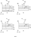
- FIG. 2 is a schematic view illustrating a signal transmission operation between the stylus pen and the touch input device.
- a touch screen 20a includes a digitizer 29, a display panel 251, a sensor unit 21, and a window 22.
- EMR electro-magnetic resonance
- the digitizer 29 may be attached to a bottom surface of the display panel 251 and include a ferrite sheet that blocks a magnetic field generated by an antenna loop and a flexible printed circuit board (FPCB) having a plurality of conductive antenna loops and an eddy current generated from other electrical elements or components when the antenna loop forms a magnetic field.
- FPCB flexible printed circuit board
- the plurality of antenna loops for detecting an input position of a resonance signal are provided as a plurality of layers.
- One antenna loop overlaps at least one another antenna loop in a Z-axis direction. Accordingly, the FPCB has a great thickness.
- the touch input device 2 is hardly reduced in thickness and size.
- the digitizer 29 When the digitizer 29 is mounted on the foldable and flexible touch input device 2, deformation may occur in the FPCB attached to an area folded when folding is generated. Repeated folding may cause stress to be applied to a wire member forming the antenna loop, thereby causing a damage to the wire member.
- the ferrite sheet blocks influence of the magnetic field generated by the antenna loop on the inside of the touch input device 2.
- the ferrite sheet may have a great thickness, be easily deformed when the touch input device 2 is folded, and be damaged by the repeated folding.
- a touch screen 20b includes a display panel 251, a sensor unit 21, and a window 22.
- a stylus pen 10 including a resonance circuit when an electrode (or pattern) of the sensor unit 21 transmits a magnetic signal B to the stylus pen, the resonance circuit contained in the stylus pen 10 resonates with the magnetic signal B. Accordingly, an electrode (or pattern) of the sensor unit 21 may receive a resonated electromagnetic signal (E and/or B) from the stylus pen 10.
- the electrode (or pattern) of the sensor unit 21 is made of a metal mesh having low resistance, a magnetic signal transmitted from the stylus pen 10 may be detected.
- a touch screen 20c does not require an additional unit or module for transmitting a magnetic signal to the stylus pen 10, thinness of the touch screen 20b may be obtained with low manufacturing costs.
- a touch screen 20c includes a loop coil 264, a display panel 251, a sensor unit 21, and a window 22.
- an electrode (or pattern) of the sensor unit 21 may receive a resonated electromagnetic signal (E and/or B) from the stylus pen 10.
- the loop coil 264 does not receive a magnetic signal B for detecting a touch position, a wire structure may be simplified, and thinness of the touch screen 20c may be obtained. Thus, thinness and miniaturization of the touch input device 2 may be obtained. Also, since the loop coil 264 may be formed in various positions with various sizes, the touch screen 20c may be also applied to the foldable/flexible touch input device 2.
- the loop coil 264 may include a substrate on which the antenna loop is disposed and a ferrite sheet.
- the antenna loop may be made of a conductive material such as copper and silver.
- the antenna loop may be disposed on the same layer as the sensor unit 21 in addition to the substrate.
- the antenna loop may be made of a conductive material having a high transmittance and a low impedance, such as a metal mesh, ITO, graphene, and a silver nanowire.
- the antenna loop may be disposed below the window. In this case, the substrate may not be contained in the loop coil 264.
- the sensor unit 21 may include a plurality of electrodes (or patterns) for detecting touch coordinates.
- the sensor unit 21 includes a plurality of first touch electrodes for detecting touch coordinates in a first direction and a plurality of second touch electrodes for detecting touch coordinates in a second direction crossing the first direction.
- the sensor unit 21 is illustrated as one layer in FIG. 2 , the first touch electrode and the second touch electrode may be disposed on different layers, may overlap each other, may not overlap each other, or may be disposed with a separate layer therebetween.
- a touch screen 20d includes a display panel 251, a sensor unit 21, and a window 22.
- the resonance circuit contained in the active stylus pen 10' resonates by using a power source (e.g., a battery for storing a power such as a secondary battery) and a capacitor such as an electric double layered capacitor (EDLC) in the active stylus pen 10'.
- a power source e.g., a battery for storing a power such as a secondary battery
- EDLC electric double layered capacitor
- the electrode of the sensor unit 21 may receive a resonated electromagnetic signal (E and/or B) from the stylus pen 10.
- E and/or B an electric double layered capacitor
- the active stylus pen 10' may include a circuit that outputs an electromagnetic signal E and/or B having a predetermined frequency using a power source in addition to a resonance circuit to generate an electromagnetic signal. Also, the active stylus pen 10' may include all of the resonance circuit and circuits that the electromagnetic signal E and/or B having a predetermined frequency.
- the touch screen 20d may receive an electromagnetic signal from the stylus pen 10' without transmitting a magnetic signal to the stylus pen 10'. That is, since the touch screen 20d does not require an additional unit or module for generating a signal for resonating the resonance circuit contained in the stylus pen 10', thinness and miniaturization of the touch screen 20d may be obtained, and power consumption and manufacturing costs may be reduced.
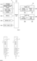
- FIG. 3 is a schematic block diagram illustrating a touch input device capable of interacting with a stylus pen.
- a touch input device 2 may include a wireless communication unit 210, a memory 220, an interface unit 230, a power supply unit 240, a display unit 250, a touch unit 260, and a control unit 270. Since components illustrated in FIG. 3 are not essential for realizing the touch input device, the touch input device described in the present disclosure may include more or less components that the above-described components.
- the wireless communication unit 210 may include at least one module for allowing wireless communication between the touch input device 2 and a wireless communication system, between the touch input device 2 and another touch input device 2, or between the touch input device 2 and an external server. Also, the wireless communication unit 210 may include at least one module connecting the touch input device 2 to at least one network.
- the wireless communication unit 210 may include a wireless internet module 211 and a short range communication module 212.
- the wireless internet module 211 refers to a module for wireless internet connection and may be incorporated in the touch input device 2.
- the wireless Internet module 211 is configured to transmit and receive a wireless signal over a communication network according to wireless internet technologies.
- the wireless internet technologies include WLAN (Wireless LAN), Wi-Fi (Wireless Fidelity) Direct, DLNA (Digital Living Network Alliance), WiBro (Wireless Broadband), WiMAX (World Interoperability for Microwave Access), HSDPA (High Speed Downlink Packet Access), HSUPA (High Speed Uplink Packet Access), NR (New Radio), LTE (Long Term Evolution), and LTE-A (Long Term Evolution-Advanced), and the wireless internet module 211 transmits and receives data according to at least one wireless internet technology within a scope including internet technologies that are not listed above.
- the short range communication module 212 is for short range communication, and at least one of BluetoothTM, RFID (Radio Frequency Identification), infrared communication (Infrared Data Association; IrDA), UWB (Ultra Wideband), ZigBee, NFC (Near Field Communication), Wi-Fi, Wi-Fi Direct, or Wireless USB (Wireless Universal Serial Bus) may be used to support the short range communication.
- the short-range communication module 212 may support wireless communication between the touch input device 2 and the wireless communication system, between the touch input device 2 and the wireless communication enabled device, or between the touch input device 2 and a network in which an external server is disposed through wireless area networks.
- the short range wireless communication network may be a short range wireless personal area networks.
- the wireless communication enabled device may be a mobile terminal (e.g., a smart phone, a tablet PC, and a notebook) capable of (or interoperable) exchanging data with the touch input device 2 according to the present invention.
- the short range communication module 212 may sense or recognize a wireless communication enabled device that is communicatable with the touch input device 2 around the touch input device 2. Further, the control unit 270 may transmit at least a portion of data processed by the touch input device 2 to the wireless communication enabled device through the short range communication module 212 when the sensed wireless communication enabled device is a device authenticated to communicate with the touch input device 2 according to an embodiment. Thus, a user of the wireless communication enabled device may use the data processed by the touch input device 2 through the wireless communication enabled device.
- the memory 220 stores data supporting various functions of the touch input device 2.
- the memory 220 may store a plurality of application programs (or applications) executed in the touch input device 2 and data for operation of the touch input device 2, and commands.
- the interface unit 230 may serve as a path to various kinds of external devices connected to the touch input device 2.
- the interface unit 230 may include at least one of a wired/wireless headset port, an external charger port, a wired/wireless data port, a memory card port, a port for connecting a device equipped with an identification module, an audio I/O (Input/Output) port, a video I/O port, and an earphone port.
- the power supply unit 240 receives external power or internal power under the control of the control unit 270 and supplies a power to each component contained in the touch input device 2.
- the power supply unit 240 may include a battery, and the battery may be an internal battery or a replaceable battery.
- the display unit 250 displays (or outputs) information processed in the touch input device 2.
- the display unit 250 may display execution screen information of an application program executed in the touch input device 2, or UI (User Interface) or GUI (Graphic User Interface) information according to the execution screen information.
- UI User Interface
- GUI Graphic User Interface
- the display unit 250 may include a LCD display (liquid crystal display), an OLED (organic light-emitting diode) display, an electronic ink display (e-ink display), a quantum dot light-emitting display, and a micro-LED (light emitting diode) display.
- LCD display liquid crystal display
- OLED organic light-emitting diode
- e-ink display electronic ink display
- quantum dot light-emitting display e.g., a quantum dot light-emitting display
- micro-LED light emitting diode
- the touch unit 260 includes a touch panel 261 including the sensor unit 21 in FIG. 2 and a touch controller 262 that transmits touch data to the control unit 270 and/or the display controller 252 by applying a driving signal to the touch panel 261 and receiving a sensing signal from the touch sensor 261.
- the touch controller 262 may be integrated into one IC with the control unit 270 that will be described later or with the display controller 252. Alternatively, the touch controller 262 may be integrated into one IC with the display controller 252 and the control unit 270. The touch controller 262 and the control unit 270, the touch controller 262 and the display controller 252, or the touch controller 262, the display controller 252, and the control unit 270 may be integrated into one and referred to as the 'control unit'.
- the display panel 251 and the touch panel 261 may form a mutual layer structure or be integrated with each other to be referred to as the touch screen 20.
- the controller 270 may control driving of the touch input device 2 and output touch coordinate information in response to a touch sensing result of the touch input device 2. Also, the control unit 270 may change a frequency of the driving signal in response to the touch sensing result.
- the controller 270 controls an overall operation of the touch input device 2 in addition to an operation related to the application program.
- the controller 270 may provide or process information or functions suitable for the user by processing a signal, data, and information inputted or outputted through the above-described components or driving the application program stored in the memory 220.
- the stylus pens of FIG. 4 commonly include a resonance circuit unit 12 in a housing thereof.
- Elements of the stylus pen 10a and 10b may be accommodated in the housing.
- the housing may have a cylindrical shape, a polygonal column shape, a column shape in which at least a portion is curved, an entasis shape, a frustum of pyramid shape, and a circular truncated cone shape, the embodiment of the present invention is not limited thereto. Since the inside of the housing is empty, the elements of the stylus pen 10a and 10b such as the resonance circuit unit 12 may be accommodated in the housing.
- the housing may be made of a non-conductive material.
- the ferrite core 115 may be, e.g., a cylindrical ferrite material.
- a through-hole which has a predetermined diameter (e.g., 1 mm) and through which the tip 11a is inserted and passes may be formed in an axial direction.
- the ferrite core 115 may have a cylindrical shape, a polygonal column shape, a column shape in which at least a portion is curved, an entasis shape, a frustum of pyramid shape, a circular truncated cone shape, a toroid shape, and a ring shape.
- the coil 116 may be wound over an entire length of the ferrite core 115 in the axial direction or wound over a partial length thereof.
- the coil 116 is electrically connected to the capacitor unit 13.
- the capacitor unit 13 may include a plurality of capacitors connected in parallel. Each of the capacitors on a printed board may have a different capacitance and be trimmed within a manufacturing process.
- the conductive tip 11b may be made of a conductive material (e.g., metal, conductive rubber, conductive fabric, or conductive silicone), the embodiment of the present invention is not limited thereto.
- a conductive material e.g., metal, conductive rubber, conductive fabric, or conductive silicone
- an inductance of the inductor unit 14 is determined by ⁇ Equation 1> below.
- L ⁇ SN 2 l
- a design of the inductor unit 14 in the resonance circuit unit 12 accommodated in the stylus pen illustrated in FIG. 4A and FIG. 4B is extremely important.
- an inductance L and a Q value are extremely important parameters as illustrated in FIG. 6 .
- L and R indicate an inductance and a resistance of the coil, respectively, and f indicates a frequency.
- the ferrite core used in this embodiment is made of manganese (Mn) and nickel (Ni).
- an enamel wire 100 that is a wire manufactured by coating a surface of a copper wire 101 with an insulating enamel 102 and heating the wire at a high temperature is used for windings or wirings of electrical devices, communication devices, and electrical instruments.
- the enamel wire having a total thickness T of 0.2 mm, a wire diameter ⁇ of 0.18 mm, and a coating thickness t of 0.01 mm is used.
- the Q values are measured for an inductor 1 and an inductor 2 , in which the enamel wire and the litz wire are respectively used as the wires of the coils, in a state in which the coil including the ferrite core made of manganese (Mn) is wound in the U-type winding scheme.
- the maximum Q value of the inductor 2 is about 1.5 times greater than that of the inductor 1.
- the litz wire is superior to the enamel wire as the coil of the inductor that forms the resonance circuit of the stylus pen.
- nickel substantially does not have relevant information in a data sheet provided by a manufacturer.
- the permittivity of manganese and nickel is measured by using the E4980A precision LCR meter of KEYSIGHT TECHNOLOGIES to check the permittivity of manganese and nickel, and measurement results are shown in table 1 below.
- Table 1 Permittivity of manganese Permittivity of nickel Measurement 1 2400 - Measurement 2 8300 2
- Measurement 1 and measurement 2 are measured by using the same E4980A precision LCR meter manufactured by KEYSIGHT TECHNOLOGIES, and the measurement 1 represents permittivity that is automatically calculated by measurement software. According to the measurement 1, it may be known that while a permittivity of manganese is 2400, a permittivity of nickel is not measured.
- FIG. 12 is a view illustrating Q values of the inductors 6 and 7 measured while changing a frequency through an E4980A precision LCR meter manufactured by KEYSIGHT TECHNOLOGIES.
- the maximum Q value of the inductor 7 (nickel core/litz wire/zigzag-type winding scheme) measured in the comparative experiment 4 almost reaches the target value Q target required for commercialization.
- the Q values are tested by manufacturing the inductors while changing a combination of the material of the ferrite core, the kind of the wire of the coil, and the winding scheme, and the test results show that the highest Q value is obtained when the inductor unit of the capacitive resonance stylus pen is designed by using the nickel core, the litz wire, and the zigzag-type winding scheme. Also, it may be known that the maximum Q value of the inductor manufactured by the above-described combination reaches the target value Q target for commercialization.
- a resistance R of a metal mesh touch sensor is approximately 1.2k ohm, and the capacitor C is approximately 250pF.
- FIG. 14 is a view for explaining that output voltages Vout1 and Vout2 of the CVA are different according to the position of the stylus pen 10 in FIG. 13 through current sensing
- FIG. 15 is a view for explaining that the output voltages Vout1 and Vout2 of the CVA are different according to the position of the stylus pen 10 in FIG. 13 through voltage sensing.
- FIG. 16 is a schematic view illustrating a touch input device according to an embodiment of the present invention.
- a touch input device includes a sensor unit 100 and a control unit 500.
- the sensor unit 100 includes a plurality of patterns (or a plurality of electrodes).
- the sensor unit 100 is an embodiment of the sensor unit 21 illustrated in FIG. 2 .
- the sensor unit 100 may include a plurality of first to fourth patterns 101, 102, 103, and 104.
- the first pattern 101 has a shape extending in a first direction.
- the first direction is illustrated as a major axis in FIG. 16 , the embodiment of the present invention is not limited thereto.
- the first direction may be a minor axis.
- the first pattern 101 may includes a plurality of main pattern parts and a connection pattern part connecting two adjacent main pattern parts among the plurality of main pattern parts.
- the main pattern part may have a diamond shape, the embodiment of the present invention is not limited thereto.
- the main pattern part may have various shapes that are different from that of the connection pattern part.
- the first pattern 101 may have an opening in which the second pattern 102 is disposed.
- the opening may have a shape corresponding to an outer shape of the first pattern 101.
- the first pattern 101 may have a structure surrounding the second pattern 102.
- the surrounding structure includes a feature in which the first pattern 101 surrounds most of the second pattern 102 except for one portion on one plane in addition to a feature in which the first pattern 101 completely surrounds the second pattern 102 on one plane.
- the first pattern 101 is spaced a predetermined distance from the second pattern 102.
- the second pattern 102 is disposed adjacent to the first pattern 101.
- the second pattern 102 may be disposed in the first pattern 101.
- the second pattern 102 may includes a plurality of main pattern parts and a connection pattern part connecting two adjacent main pattern parts among the plurality of main pattern parts.
- the main pattern part may have a diamond shape, the embodiment of the present invention is not limited thereto.
- the main pattern part may have various shapes that are different from that of the connection pattern part.
- the main pattern part of the second pattern 102 may have a shape corresponding to that of the main pattern part of the first pattern 101, and the connection pattern part of the second pattern 102 may have a shape corresponding to that of the connection pattern part of the first pattern 101.
- the plurality of first patterns 101 have one ends electrically connected to the control unit 500 and the other ends that are electrically opened.
- each of the one ends is relatively close to the control unit 500, and each of the other ends is relatively far from the control unit 500.
- one end may be referred to as a first end, and the other end may be referred to as a second end.
- the one ends of the plurality of first patterns 101 may be electrically connected to the control unit 500 through a conductive trace.
- the plurality of second patterns 102 may have one ends electrically connected to the control unit 500 and the other ends that are electrically connected to each other through vias.
- the vias of the other ends of the plurality of second patterns 102 may be electrically connected to each other through a conductive trace.
- each of the one ends is relatively close to the control unit 500, and each of the other ends is relatively far from the control unit 500.
- a total impedance is reduced because a capacitances for each second pattern 102 is added.
- an effect in which each of the other ends of the plurality of second patterns 102 is AC GND is obtained.
- the other ends of the plurality of second patterns 102 which are electrically connected to each other, may be grounded.
- the other ends of the plurality of second patterns 102 may not be electrically connected to each other, and a predetermined capacitor may be connected to each of the other ends of the second patterns 102.
- At least a portion of the first pattern 101 and at least a portion of the second pattern 102 are disposed on the same layer.
- the first pattern 101 and the second pattern 102 may be disposed on the same layer.
- the first pattern 101 and the second pattern 102 may be formed on the same layer by using a metal mesh.
- the third pattern 103 has a shape extending in a second direction.
- the second direction is illustrated as a minor axis in FIG. 16 , the embodiment of the present invention is not limited thereto.
- the second direction may be a major axis.
- the third pattern 103 may includes a plurality of main pattern parts and a connection pattern part connecting two adjacent main pattern parts among the plurality of main pattern parts.
- the main pattern part may have a diamond shape, the embodiment of the present invention is not limited thereto.
- the main pattern part may have various shapes that are different from that of the connection pattern part.
- the third pattern 103 may have an opening in which the fourth pattern 104 is disposed.
- the opening may have a shape corresponding to an outer shape of the third pattern 103.
- the third pattern 103 may have a structure surrounding the fourth pattern 104.
- the third pattern 103 is spaced a predetermined distance from the fourth pattern 104.
- the fourth pattern 104 is disposed adjacent to the third pattern 103.
- the fourth pattern 104 may be disposed in the third pattern 103.
- the fourth pattern 104 may includes a plurality of main pattern parts and a connection pattern part connecting two adjacent main pattern parts among the plurality of main pattern parts.
- the main pattern part may have a diamond shape, the embodiment of the present invention is not limited thereto.
- the main pattern part may have various shapes that are different from that of the connection pattern part.
- the main pattern part of the fourth pattern 104 may have a shape corresponding to that of the main pattern part of the third pattern 103, and the connection pattern part of the fourth pattern 104 may have a shape corresponding to that of the connection pattern part of the third pattern 103.
- a plurality of the third patterns 103 and a plurality of fourth patterns 104 are disposed in parallel to each other.
- the plurality of third patterns 103 have one ends electrically connected to the control unit 500 and the other ends that are electrically opened. Here, each of the one ends is relatively close to the control unit 500, and each of the other ends is relatively far from the control unit 500.
- the one ends of the plurality of third patterns 103 may be electrically connected to the control unit 500 through a conductive trace.
- the plurality of fourth patterns 104 may have one ends electrically connected to the control unit 500 and the other ends that are electrically connected to each other through vias.
- the vias of the other ends of the plurality of fourth patterns 104 may be electrically connected to each other through a conductive trace.
- each of the one ends is relatively close to the control unit 500, and each of the other ends is relatively far from the control unit 500.
- total impedance is reduced because a capacitance for each fourth pattern 104 is added.
- an effect in which each of the other ends of the plurality of fourth patterns 104 is AC GND is obtained.
- the other ends of the plurality of fourth patterns 104 which are electrically connected to each other, may be grounded.
- the other ends of the plurality of fourth patterns 104 may not be electrically connected to each other, and a predetermined capacitor may be connected to each of the other ends of the fourth patterns 104.
- At least a portion of the third pattern 103 and at least a portion of the fourth pattern 104 are disposed on the same layer.
- the third pattern 103 and the fourth pattern 104 may be disposed on the same layer.
- the third pattern 103 and the fourth pattern 104 may be formed on the same layer by using a metal mesh.
- the third pattern 103 and the fourth pattern 104 may be disposed on a layer different from that of the first pattern 101 and the second pattern 102.
- the first pattern 101 and the second pattern 102 may be disposed on a first layer
- the third pattern 103 and the fourth pattern 104 may be disposed on a second layer that is different from the first layer.
- the control unit 500 may be electrically connected to the sensor unit 100 and control an operation of the sensor unit 100.
- the control unit 500 and the sensor unit 100 may be electrically connected to each other through a conductive trace.
- control unit 500 is the touch controller 262 illustrated in FIG. 3
- the embodiment of the present invention is not limited thereto.
- the control unit 500 may be obtained by: integrating the touch controller 262 and the display controller 252 in FIG. 3 ; integrating the touch controller 262 and the control unit 270 in FIG. 3 ; or integrating the touch controller 262, the display controller 252, and the control unit 270 in FIG. 3 .
- the control unit 500 may be a separate controller contained in the sensor unit 100.
- the control unit 500 according to the present invention is not limited to the touch controller 262 or the control unit 270 in FIG. 3 , and a component capable of controlling a sensor unit according to following embodiments in addition to the sensor unit 100 may be referred to as a 'controller'.
- the control unit 500 may include a plurality of driving circuit units and a plurality of sensing circuit units.
- the plurality of driving circuit units may include a driving circuit unit for touch sensing and a driving circuit unit for stylus driving.
- the plurality of sensing circuit units may include a sensing circuit unit for touch sensing and a sensing circuit unit for stylus sensing.
- some sensing circuit units among the plurality of sensing circuit units may perform touch sensing in addition to stylus sensing.
- the control unit 500 may control the sensor unit 100 to operate in one of a touch sensing mode, an antenna driving mode, and a stylus pen sensing mode.
- the control unit 500 may connect the plurality of the driving/sensing circuit units to the sensor unit 100 according to each mode and control the driving signal to be applied to the plurality of driving circuit units.
- the control unit 500 may include a plurality of switches for electrically connecting the plurality of driving/sensing circuit units and the sensor unit 100.
- FIG. 17 is a view illustrating a case in which the touch input device illustrated in FIG. 16 operates in the touch sensing mode (or 2D sensing mode).
- the control unit 500 simultaneously or sequentially applies a driving signal (or, touch driving signal) for the touch sensing to at least one first pattern among the plurality of first patterns 101 and receives a sensing signal (or, touch sensing signal) received from at least one third pattern among the plurality of third patterns 103.
- the plurality of sensing circuit units of the control unit 500 electrically connected to the plurality of third patterns 103 may output information on capacitance variation contained in the input sensing signal as a predetermined voltage value.
- the control unit 500 may process the outputted voltage value to detect a touch position.
- control unit 500 is not electrically connected to the plurality of second patterns 102
- the plurality of driving circuit units may be electrically connected to the plurality of second patterns 102 so that capacitive coupling is not generated between the first pattern 101 and the second pattern 102.
- the control unit 500 may control the same driving signal as the driving signal applied to the plurality of first patterns 101 to be applied to the plurality of second patterns 102.
- the control unit 500 may control a predetermined reference potential to be applied to the plurality of second patterns 102 when the driving signal is applied to the plurality of first patterns.
- FIG. 18 is a view illustrating a case in which the touch input device illustrated in FIG. 16 operates in the antenna driving mode (or stylus pen driving mode, or stylus uplink mode).
- the control unit 500 may electrically connect the plurality of driving circuit units for antenna driving to the plurality of second patterns 102 of the sensor unit 100.
- the control unit 500 may control a plurality of switches sw to electrically connect the conductive traces connected to the plurality of second patterns 102 with the plurality of driving circuit units.
- the control unit 500 may control the driving signal (or pen driving signal) outputted to each driving circuit unit connected to the plurality of second patterns 102.
- FIGS. 19A to 19C are views for describing various methods by which the control unit 500 applies a pen driving signal for driving the stylus pen to the plurality of second patterns 102 illustrated in FIG. 16 .
- one second pattern 102 in FIG. 16 is simply illustrated as one line Ch, and each line Ch is one channel
- FIG. 19A shows a case in which a stylus pen 50 is disposed on a central portion (an area except for an edge) of the sensor unit 100 in FIG. 16 .
- the stylus pen 50 is disposed on a fifth channel Ch5.
- the control unit 500 may control a plurality of driving circuit units so that a pulse signal and a reverse pulse signal (or ground) are applied to the same number of channels Ch2, Ch3, Ch4 / Ch6, Ch7, Ch8 on left and right sides based on a position on which the stylus pen 50 is disposed.
- control unit 500 controls the pulse signal to be applied to the three second to fourth channels Ch2, Ch3, and Ch4 disposed on the left side of the stylus pen 50 and the reverse pulse signal to be applied to the three sixth to eighth channels Ch6, Ch7, and Ch8 disposed at the right side of the stylus pen 50.
- the pulse signal and the reverse pulse signal are applied to the three channels on each of the left and right sides with respect to the stylus pen 50 in FIG. 19A
- the embodiment of the present invention is not limited thereto. For example, in FIG.
- the pulse signal and the reverse pulse signal may be applied to two channels or one channel on each of the left and right sides with respect to the stylus pen 50, or the pulse signal and the reverse pulse signal (or ground) may be applied to four or more channels.
- FIG. 19B shows a case in which the stylus pen 50 is disposed on the edge of the sensor unit 100 in FIG. 16 .
- the stylus pen 50 is disposed between a 0-th channel Ch0 and a first channel Ch1.
- the control unit 500 may not apply the pulse signal and the reverse pulse signal (or ground) to the same number of channel(s) on each of the left and right sides with respect to the stylus pen 50.
- the control unit 500 may control the pulse signal and the reverse pulse signal (or ground) to be applied to the different number of channels on the left and right sides with respect to the stylus pen 50.
- control unit 500 may control the pulse signal to be applied to the 0-th channel Ch0 and the reverse pulse signal to be applied to the first to third channels Ch1, Ch2, and Ch3.
- the control unit 500 may control the reverse pulse signal to be applied to the 0-th to second channels Ch0, Ch1, and Ch2.
- FIGS. 19A and 19B As the number of channels Ch0, Ch1, ..., Ch19 increases, the number of terminals of the control unit 500 for driving each channel increases, and a configuration of the driving circuit unit becomes complicated. Thus, at least two or more channels adjacent to each other among the channels Ch0, Ch1, ..., Ch19 may be electrically connected and driven as one channel. Specifically, as illustrated in (c) of FIG. 19 , two channels are electrically connected to form one channel. In this configuration, the same signal is simultaneously applied to the two electrically connected channels.
- FIG. 19C shows a case in which 20 channels Ch0, Ch1, ..., Ch19 are electrically connected for each two channels to form 10 channels. Although not shown in the drawing, seven channels may be configured such that the 20 channels are electrically connected for each three channels and the rest two channels are electrically connected, and five channels may be configured such that the 20 channels are electrically connected for each four channels.
- FIG. 20 is a view illustrating a case in which the touch input device illustrated in FIG. 16 operates in the stylus pen sensing mode (or stylus downlink mode).
- the control unit 500 may electrically connect the plurality of sensing circuit units for stylus sensing to the first pattern 101 and the third pattern 103 of the sensor unit 102.
- the control unit 500 may control a plurality of switches sw to electrically connect the conductive traces connected to the plurality of first patterns 101 and the plurality of third patterns 103 with the plurality of sensing circuit units.
- the touch input device has an advantage in that an output voltage value of the plurality of sensing circuit units is hardly changed according to the position of the stylus pen on the sensor unit 100 in the stylus pen sensing mode due to the configuration of the sensor unit 100. A specific principle for this will be described with reference to FIGS. 21A to 21F .
- FIGS. 21A to 21F are schematic views for explaining an operation principle of the stylus pen sensing mode of FIG. 20
- FIG. 21A is a schematic circuit diagram of modeling one first pattern 101 in FIG. 20 and the sensing circuit unit of the control unit 500 electrically connected thereto
- FIG. 21B is a schematic circuit diagram of modeling the second pattern 102 disposed in one first pattern 101.
- FIG. 21C is a voltage distribution graph in the circuit diagram of FIG. 21A
- FIG. 21D is a voltage distribution graph in the circuit diagram of FIG. 21B .
- a voltage Vemf (hereinafter, referred to as an 'induced voltage') induced by a signal emitted from the stylus pen is generated at the corresponding point A .
- FIGS. 21C and 21D it may be known that a potential difference as much as the voltage Vemf exists at any position between the first pattern 101 and the second pattern 102.
- the potential difference as much as the voltage Vemf between the first pattern 101 and the second pattern 102 causes capacitive coupling between the first pattern 101 and the second pattern 102.
- FIG. 21E current flows from the second pattern 102 to the first pattern 101 by the capacitive coupling.
- FIG. 21E current flows from the second pattern 102 to the first pattern 101 by the capacitive coupling.
- control unit 500 may sense the position of the stylus pen through the sensing circuit unit electrically connected to the first pattern 101 and the third pattern 103.
- the control unit 500 may sense the stylus pen from a constant signal outputted from the sensing circuit unit regardless of whether the position of the stylus pen on the sensor unit 100 is close to or far from the sensing circuit unit.
- the embodiment of the present invention is not limited thereto.
- current may be also introduced to the first pattern 101 from the second pattern 102 by magnetic coupling (magnetic field coupling).
- Various combinations of the plurality of first to fourth patterns 101, 102, 103, and 104 may be used so that the sensor unit 100 of the touch input device shown in FIG. 16 drives and senses the stylus pen.
- the various combinations are shown in ⁇ Table 2> below.
- ⁇ Table 2> below '1' represents the plurality of first patterns 101, '2' represents the plurality of second patterns 102, '3 represents the plurality of third patterns 103, and '4 ' represents the plurality of fourth patterns 104.
- Finger Touch Stylus uplink signal magnitude downlink signal magnitude Stylus additional channel Operation Operation Driving Sensing Driving Sensing Tx Rx Major axis Minor axis X-axis Y-axis Major axis Minor axis X-axis Y-axis Driving Sensing 1 1 3 2 1 3 Small Small Small Yes No 2 1 3 2 1 4 Large Small Large Yes Yes 3 1 3 2 2 3 Large Large Small Yes Yes 4 1 3 2 2 4 Large Large Large Yes 5 1 3 4 1 3 Large Small Small Yes No 6 1 3 4 1 4 Large Small Large Yes 7 1 3 4 2 3 Large Small Yes Yes 8 1 3 4 2 4 Large Large Large Yes 9 1 3 2 4 1 3 Large Large Small Small Yes No 10 1 3 2 4 1 4 Large Large Small Large Yes 11 1 3 2 4 2 3 Large Large Large Small Yes Yes 12 1 3 2 4 2 4 Large Large Large Large Yes 13 1 3 1 1 3 Small Small Small No No 14 1 3 1 1 4 Small Small Large No Yes 15 1 3 1 2 3 Small Large Small No Yes 16 1 3 1 2 4 Small Large
- the plurality of first patterns 101 and the plurality of third patterns 103 sense a touch of an object such as a finger.
- the plurality of first patterns 101 operate as touch driving electrodes
- the plurality of third patterns 103 operate as touch receiving electrodes by the control unit 500.
- the plurality of first patterns 101 may operate as the touch receiving electrodes
- the plurality of third patterns 103 may operate as the touch driving electrodes by the control unit 500.
- One or two of the plurality of first to fourth patterns 101, 102, 103, and 104 may operate as a stylus driving electrode for driving the stylus pen by the control unit 500.
- One or two of the plurality of first to fourth patterns 101, 102, 103, and 104 may be used to form a current loop for driving the stylus pen.
- An X-axis driving may be performed by one of the plurality of first patterns 101 and the plurality of second patterns 102
- a Y-axis driving may be performed by one of the plurality of third patterns 103 and the plurality of fourth patterns 104.
- the driving of the stylus pen may be performed by either the X-axis driving or the Y-axis driving or by both the X-axis driving and the Y-axis driving.
- At least two of the plurality of first to fourth patterns 101, 102, 103, and 104 may operate as a sensing electrode for sensing a stylus pen signal emitted from the stylus pen. Since both X-axis sensing and Y-axis sensing are required to sense the stylus pen signal, two of the plurality of first to fourth patterns 101, 102, 103, and 104 are used. An X-axis sensing may be performed by one of the plurality of first patterns 101 and the plurality of second patterns 102, and a Y-axis sensing may be performed by one of the plurality of third patterns 103 and the plurality of fourth patterns 104.
- the 'magnitude of uplink signal' represents a magnitude of a driving signal for driving the stylus pen.
- the uplink signal is relatively greater when the stylus pen driving signal is applied to the plurality of second patterns 102 than when the stylus pen driving signal is applied to the plurality of first patterns 101.
- the other ends of the plurality of first patterns 101 are not electrically connected not to form a current loop while the other ends of the plurality of second patterns 102 are electrically connected to form at least one current loop when two or more second patterns to which the stylus pen driving signal is applied are properly selected.
- the current may not flow smoothly from one end to the other end of each first pattern 101.
- a stylus pen driving signal applied through the plurality of first patterns 101 is transmitted to the plurality of second patterns 101 in which the current loop is formed through the capacitive coupling.
- signal attenuation occurs by the capacitive coupling.
- the uplink signal is relatively greater when the stylus pen driving signal is applied to the plurality of fourth patterns 104 than when the stylus pen driving signal is applied to the plurality of third patterns 103.
- the 'magnitude of downlink signal' represents a magnitude of stylus pen signal received from the stylus pen.
- the downlink signal is relatively greater when the stylus pen driving signal is received by the plurality of second patterns 102 than when the stylus pen driving signal is received by the plurality of first patterns 101.
- the other ends of the plurality of second patterns 102 are electrically connected to form a current loop
- the other ends of the plurality of first patterns 101 are not electrically connected to each other, particularly, the stylus pen signal is transmitted to the plurality of first patterns 101 from the plurality of second patterns 101 in which the current loop is formed through the capacitive coupling, and thus attenuation of the downlink signal occurs.
- the downlink signal is relatively greater when the stylus pen signal is received through the plurality of fourth patterns 104 than when the stylus pen signal is received through the plurality of third patterns 103.
- the 'stylus additional channel' represents whether an additional channel is necessary for the stylus pen in addition to the touch sensing.
- an additional channel is required (marked by 'Yes' in the ⁇ Table 2>).
- the plurality of first patterns 101 and/or the plurality of third patterns 103 for touch sensing are used for driving or sensing the stylus pen, an additional channel is not required (marked by 'No' in the ⁇ Table 2>).
- the uplink signal has a relatively large magnitude. Since the plurality of first patterns 101 and the plurality of third patterns 103 are used as the stylus sensing electrode, the downlink signal has a relatively small magnitude. Also, since the plurality of second patterns 102 are separately used as the stylus driving electrode, an additional channel for driving the stylus pen is required, but an additional channel for sensing the stylus pen is not required.
- the plurality of first patterns 101 are used as the touch driving electrode for sensing the touch of the object.
- the plurality of second patterns 102 are used as the stylus sensing electrode for sensing the stylus pen signal as well as the stylus driving electrode for driving the stylus pen.
- the plurality of third patterns 103 are used as the touch sensing electrode for sensing the touch of the object.
- the plurality of fourth patterns 104 are used as the stylus sensing electrode for sensing the stylus pen signal.
- the uplink signal has a relatively large magnitude. Since the plurality of second patterns 102 and the plurality of fourth patterns 104 are used as the stylus sensing electrode, the downlink signal has a relatively large magnitude. Also, since the plurality of second patterns 102 are separately used as the stylus sensing electrode, and the plurality of fourth patterns 104 are separately used as the stylus driving electrode and the stylus sensing electrode, a separate additional channel is required for driving and sensing the stylus pen.
- the uplink signal has a relatively large magnitude. Since the plurality of first patterns 101 and the plurality of third patterns 103 are used as the stylus sensing electrode, the downlink signal has a relatively small magnitude. Also, since the plurality of first patterns 101 are separately used as the stylus driving electrode and the stylus sensing electrode, and the plurality of third patterns 103 are used as the stylus sensing electrode, a separate additional channel is not required for driving and sensing the stylus pen.
- the plurality of second patterns 102 are used for operating the sensor unit 100 in FIG. 16 in the antenna driving mode in FIG. 18
- the plurality of first patterns 101 and the plurality of third patterns 103 are used for driving the sensor unit 100 in the antenna driving mode in FIG. 23 .
- the control unit 500 may control the stylus pen driving signal to be applied to the plurality of first patterns 101 and the plurality of third patterns 103 or control the stylus pen driving signal to be applied to the plurality of third patterns 103 after the stylus pen driving signal is applied to the plurality of first patterns 101.
- the opposite case may be true.
- FIG. 24 is a view for explaining another example in which the sensor unit 100 in FIG. 16 operates in the stylus pen sensing mode.
- the control unit 500 may sense the stylus pen receiving signal received from the plurality of second patterns 102 and the plurality of fourth patterns 104 to detect a position of the stylus pen in the stylus pen sensing mode.
- the sensor unit 100' includes a plurality of patterns.
- the plurality of patterns may include a first-a pattern 101a, a first-b pattern 101b, a second- a pattern 102a, a second-b pattern 102b, a third pattern 103, and a fourth pattern 104.
- the third pattern 103 and the fourth pattern 104 have the same configuration as the third pattern part 103 and the fourth pattern part 104 of the sensor unit 100 illustrated in FIG. 16 , a description thereof will be omitted.
- the second-a pattern 102a may include an inverted triangle pattern part, a triangle pattern part, and a connection pattern part connecting the inverted triangle pattern part and the triangular pattern part.
- the first-b pattern 101b has a shape extending along the first direction (or major axis).
- the first-b pattern 101b may include an inverted triangle pattern part, a triangle pattern part, and a connection pattern part connecting the inverted triangle pattern part and the triangular pattern part.
- the first-b pattern 101b may have an opening in which the second-b pattern 102b is disposed.
- the second-b pattern 102b is disposed adjacent to the first-b pattern 101b.
- the second-b pattern 102b is disposed in the first-b pattern 101b.
- the second-b pattern 102b may include an inverted triangle pattern part, a triangle pattern part, and a connection pattern part connecting the inverted triangle pattern part and the triangular pattern part.
- a plurality of the first-a patterns 101a and a plurality of the first-b patterns 101b are alternately arranged along the first direction, the plurality of the first-a patterns 101a are electrically connected each other, and the plurality of the first-b patterns 101b are also electrically connected to each other.
- the first-a pattern 101a disposed at one end of the plurality of the first-a patterns 101a is electrically connected to the control unit 500'.
- the first-b pattern 101b disposed at one end of the plurality of the first-b patterns 101b is electrically connected to the control unit 500'.
- a plurality of the second-a patterns 102a and a plurality of the second-b patterns 102b are alternately arranged in the first direction and electrically connected to each other.
- the second-b pattern 102b disposed at one end of the plurality of the second-b patterns 102b may be electrically connected to the control unit 500', and the second-a pattern 102a disposed at the other end of the plurality of the second-a patterns 102a may be electrically connected to other adjacent second-a patterns.
- other second-a patterns adjacent to the second-a pattern 102a disposed at the other end may be grounded.
- the first-a pattern 101a, the first-b pattern 101b, the second-a pattern 102a, and the second-b pattern 102b may be disposed on the same layer.
- the first-a pattern 101a, the first-b pattern 101b, the second-a pattern 102a, and the second-b pattern 102b may be formed on the same layer by using a metal mesh.
- the control unit 500' has the same function as the controller unit 500 in FIG. 16 .
- FIG. 28 is a view illustrating a case in which the touch input device illustrated in FIG. 27 operates in the touch sensing mode (or 2D sensing mode).
- control unit 500' may electrically connect the driving circuit unit for touch sensing to the third pattern 103 of the sensor unit 100'.
- One driving circuit unit may be electrically connected to each of the plurality of the third patterns 103.
- control unit 500' may electrically connect the sensing circuit unit for touch sensing to the first-a and first-b patterns 101a and 101b of the sensor unit 100'.
- the control unit 500' applies a driving signal for touch sensing to the plurality of the third pattern 103 and receives a sensing signal received from the plurality of the first-a and the first-b patterns 101a and 101b.
- the sensing circuit unit of the control unit 500' electrically connected to the plurality of first-a and first-b patterns 101a and 101b may output information on capacitance variation contained in the input sensing signal as a predetermined voltage value.
- the control unit 500' may process the outputted voltage value to detect a touch position.
- the control unit 500' may cancel a display noise and a LGM noise by subtracting the sensing signal received from the first-b pattern 101b from a sensing signal received from the first-a pattern 101a.
- control unit 500' may electrically connect the driving circuit unit for antenna driving to the plurality of second-a and second-b patterns 102a and 102b of the sensor unit 100'.
- control unit 500' may control the driving signal to be applied to the plurality of first-a and first-b patterns 101a and 101b and/or the third pattern 103. In this case, the total number of channels may be reduced.
- control unit 500' may electrically connect the sensing circuit unit for stylus sensing to the first-a and first-b patterns 101a and 101b and the third pattern 103 of the sensor unit 100'.
- a predetermined signal is outputted from the stylus pen, and an induced voltage is generated in the first-a, first-b, second-a, second-b, third, and fourth patterns 101a, 101b, 102a, 102b, 103, and 104 by the outputted signal.
- control unit 500' may detect the position of the stylus pen through the sensing circuit unit electrically connected to the plurality of first-b patterns 101b.
- control unit 500' may detect the position of the stylus pen through the sensing circuit unit electrically connected to the third pattern 103.
- control unit 500' may electrically connect the sensing circuit units to the plurality of second-a and second-b patterns 102a and 102b and/or the fourth pattern 104 to detect the position of the stylus pen.
- the first-b pattern disposed at the other side (upper side) among the plurality of first-b patterns 101b electrically connected to each other in the first direction is electrically opened
- the first-a pattern disposed at one side (lower side) among the plurality of first-a patterns 101a electrically connected to each other in the first direction is electrically opened.
- FIG. 32 is a view illustrating a case in which the touch input device illustrated in FIG. 31 operates in the touch sensing mode (or 2D sensing mode).
- FIG. 34 is a view illustrating a case in which the touch input device illustrated in FIG. 31 operates in the stylus sensing mode (or stylus downlink mode).
- the stylus sensing mode of FIG. 34 is different from that of FIG. 30 .
- the control unit 500 may detect the position of the stylus pen through the sensing circuit unit electrically connected to the plurality of first-b patterns 101b.
- the feature in which current is introduced from the second-b patterns 102b and the first-a patterns 101a to the first-b patterns 101b is caused by capacitive coupling between the first-b patterns 101b and the second-b pattern 102b and capacitive coupling between the first-b patterns 101b and the first-a pattern 101a, which occur by potential differences generated as much as the induced voltage between the first-b patterns 101b and the second-b patterns 102b and between the first-b patterns 101b and the first-a patterns 101a.
- a reason why current is introduced from the first-a pattern 101a to the first-b pattern 101b is that a relatively large amount of current flows through the plurality of first-a patterns 101a themselves. This is because a direction of conductive traces connected to the plurality of first-a patterns 101a is opposite to that of conductive traces connected to the plurality of first-b patterns 101b. In other words, when the stylus pen is spaced apart from the sensing circuit unit connected to the plurality of first-b patterns 101b, the stylus pen is disposed closer to the sensing circuit unit connected to the plurality of first-a patterns 101a.
- control unit 500" may detect the position of the stylus pen through the sensing circuit unit electrically connected to the third pattern 103.
- control unit 500' may electrically connect the sensing circuit units to the plurality of second-a patterns 102a, the plurality of second-b patterns 102b, or the fourth pattern 104 to detect the position of the stylus pen.
- FIG. 35 is a table showing characteristics of various embodiments illustrated in FIGS. 16 , 27 , and 31 .
- the embodiment of FIG. 16 may include total 70 to 80 channels.
- a driving electrode TX used in the touch sensing mode may include 20 channels
- a receiving electrode RX may include 40 channels
- an antenna driving electrode TX used in the antenna driving mode may include 10 to 20 channels.
- the antenna driving mode includes 10 channels, two adjacent channels may be connected in parallel.
- FIG. 16 may include 20 left conductive traces and 20 right conductive traces in the second direction (minor axis).
- a width of a bezel of the touch input device may be maintained as same as an original width thereof.
- the embodiment of FIG. 27 may include total 90 to 100 channels.
- a driving electrode TX used in the touch sensing mode may include 40 channels
- a receiving electrode RX may include 40 channels
- an antenna driving electrode TX used in the antenna driving mode may include 10 to 20 channels.
- the antenna driving mode includes 10 channels, two adjacent channels may be connected in parallel.
- FIG. 27 may include 20 left conductive traces and 20 right conductive traces in the second direction (minor axis).
- a width of a bezel of the touch input device may be maintained as same as an original width thereof.
- the embodiment of FIG. 31 may include total 90 to 100 channels.
- a driving electrode TX used in the touch sensing mode may include 40 channels
- a receiving electrode RX may include 40 channels
- an antenna driving electrode TX used in the antenna driving mode may include 10 to 20 channels.
- the antenna driving mode includes 10 channels, two adjacent channels may be connected in parallel.
- FIG. 31 may include 30 left conductive traces and 30 right conductive traces in the second direction (minor axis).
- FIG. 36 is a partial plan view of a sensor unit 200 according to another embodiment, which may replace the sensor unit 100 of FIG. 16
- the sensor unit 200 includes a plurality of first patterns and a plurality of second patterns.
- the plurality of first patterns will be described as a plurality of driving electrodes TX0, TX1, TX2,...
- the plurality of second patterns will be described as a plurality of receiving electrodes RX0, RX1, RX2,....
- the plurality of first electrodes may be a plurality of receiving electrodes RX0, RX1, RX2,...
- the plurality of second electrodes may be a plurality of driving electrodes TX0, TX1, TX2,....
- the plurality of driving electrodes TX0, TX1, TX2,... may have a shape extending in a fist direction (or horizontal direction), and the plurality of receiving electrodes RX0, RX1, RX2,... may have a shape extending in a second direction (or vertical direction) perpendicular to the first direction.
- a predetermined capacitance is formed between the plurality of driving electrodes TX0, TX1, TX2,... and the plurality of receiving electrodes RX0, RX1, RX2,..., particularly at a crossing portion therebetween.
- the capacitance is varied when a touch input is generated at a corresponding point or a surrounding thereof.
- whether a touch is generated or a touch input may be detected by detecting an amount of a capacitance variation from a signal outputted from the plurality of receiving electrodes RX0, RX1, RX2,....
- Each of the plurality of driving electrodes TX0, TX1, TX2,... in FIG. 36 includes a first driving pattern part 211, a second driving pattern part 213, and a connection pattern 215.
- the first driving pattern part 211 may be referred to as a first-1 pattern part
- the second drive pattern part 213 may be referred to as a first-2 pattern part
- the connection pattern 215 may be referred to as a connection pattern part.
- the first driving pattern part 211 has a diamond shape or a rhombus shape and includes an opening O.
- the opening O has a diamond shape or a rhombus shape corresponding to an outer shape of the first driving pattern part 211.
- the first driving pattern part 211 may have a diamond or rhombus band shape by the opening O.
- the first driving pattern part 211 has a diamond or rhombus shape in the drawings, this is merely an example.
- the first driving pattern part 211 may have a polygonal or rectangular shape.
- the second driving pattern part 213 is disposed adjacent to the first driving pattern part 211.
- the second driving pattern part 213 may have a diamond shape or a rhombus shape.
- the second driving pattern part 213 may have an outer shape corresponding to that of the first driving pattern part 211.
- the second driving pattern part 213 may not have an opening therein unlike the first driving pattern part 211.
- the first driving pattern part 211 and the second driving pattern part 213 are spaced a predetermined distance from each other.
- the first driving pattern part 211 in which the second driving pattern part 213 is disposed is provided in plurality and arranged in the first direction (or horizontal direction).
- the connection patterns 215 disposed between the plurality of first driving pattern parts 211 electrically connect the plurality of first driving pattern parts 211 to each other.
- connection pattern 215 connects two adjacent first driving pattern parts 211. One end is connected to the first driving pattern part 211 disposed at one side, and the other end is connected to the first driving pattern part 211 disposed at the other side.
- connection pattern 215 may have a bar shape, the embodiment of the present invention is not limited thereto.
- the connection pattern 215 may have various shapes connecting two adjacent first driving pattern parts 211.
- At least a portion of the plurality of first driving pattern parts 211, at least a portion of the plurality of second driving pattern parts 213, and at least a portion of the plurality of connection patterns 215 are disposed on the same layer.
- the plurality of first driving pattern parts 211, the plurality of second driving pattern parts 213, and the plurality of connection patterns 215 may be disposed on the same layer.
- the plurality of first driving pattern parts 211, the plurality of second driving pattern parts 213, and the plurality of connection patterns 215 may be made of the same material.
- the plurality of first driving pattern parts 211, the plurality of second driving pattern parts 213, and the plurality of connection patterns 215 may be made of a metal mesh.
- the metal mesh is patterned according to shapes of the shapes of the plurality of first driving pattern parts 211, the plurality of second driving pattern parts 213, and the plurality of connection patterns 215, the plurality of driving electrodes TX0, TX1, TX2,... may be formed.
- Each of the plurality of receiving electrodes RX0, RX1, and RX2 includes a first receiving pattern part 231 and a second pattern part 233.
- the first driving pattern part 231 may be referred to as a second-1 pattern part
- the second receiving pattern part 233 may be referred to as a second-2 pattern part.
- first driving pattern part 231 and the second driving pattern part 233 have the same shape as the first driving pattern part 211 and the second driving pattern part 213, a detailed description thereof will be omitted.
- a plurality of first receiving pattern parts 231 are arranged in the second direction (or vertical direction).
- the plurality of first receiving pattern parts 231 are electrically connected to each other.
- the plurality of first receiving pattern parts 231 are electrically connected through a bridge or a via.
- a plurality of second receiving pattern parts 233 are arranged in the first receiving pattern parts 231, respectively, in the second direction (or vertical direction).
- the plurality of second receiving pattern parts 233 are electrically connected to each other.
- the plurality of second receiving pattern parts 233 are electrically connected through a bridge or a via.
- the first receiving pattern parts 231 disposed at the other edge among the first receiving pattern parts 231 of each of the receiving electrodes RX0, RX1, and RX2 are electrically opened, and the second receiving pattern parts 233 disposed at the other edge among the second receiving pattern parts 233 of each of the receiving electrodes RX0, RX1, and RX2 may be electrically connected.
- the plurality of second receiving pattern parts 233 are electrically connected through a bridge or a via.
- the other side represents a farthest side from the control unit 500 of FIG. 16 among the first and second receiving pattern parts 231 and 233 of each of the receiving electrodes RX0, RX1, and RX2.
- At least a portion of the plurality of first receiving pattern parts 231 and at least a portion of the plurality of second receiving pattern parts 233 are disposed on the same layer.
- the plurality of first receiving pattern parts 231 and the plurality of second receiving pattern parts 233 may be disposed on the same layer.
- the plurality of first receiving pattern parts 231 and the plurality of second receiving pattern parts 233 may be disposed on the same layer with the plurality of first driving pattern parts 211, the plurality of second driving pattern parts 213, and the plurality of connection patterns 215.
- Bridges for electrically connecting the second driving pattern parts 213 of each of the driving electrodes TX0, TX1, and TX2 and bridges for electrically connecting the first and second receiving pattern parts 231 and 233 of each of the receiving electrodes RX0, RX1, and RX2 may be formed on a layer different from that on which the first and second driving pattern parts 211 and 213, the connection pattern 215, and the first and second receiving pattern parts 231 and 233 are formed.
- the sensor unit 200 in FIG. 36 may be driven in one of the touch sensing mode, the antenna driving mode, and the stylus sensing mode by the control unit 500.
- the control unit 500 may control the touch driving signal to be applied to at least one of ATX1, ATX2, and ATX3 and sense a touch position by receiving a touch reception signal from at least one of ARX1, ARX2, and ARX3.
- the control unit 500 may apply the pen driving signal to at least one of DTX1, DTX2, and DTX3 or at least one of DRX1, DRX2, and DRX3.
- the control unit 500 may sense the position of the stylus pen by receiving the pen reception signal from at least one of ATX1, ATX2, and ATX3 and at least one of ARX1, ARX2, and ARX3. Also, the various combinations of the ⁇ table 2> may be applied to the sensor unit 200 of FIG. 36 . Thus, the sensor unit 200 of FIG. 36 may be driven in one of the touch sensing mode, the antenna driving mode, and the stylus sensing mode through various methods by the control unit 500.
- FIG. 37 is a partial plan view of a sensor unit 200' according to another embodiment, which may replace the sensor unit 100 of FIG. 16
- the sensor unit 200' of FIG. 37 includes a plurality of driving electrodes TX0', TX1', TX2',... and a plurality of receiving electrodes RX0, RX1, RX2,....
- the plurality of receiving electrodes RX0, RX1, RX2,... are the same as the plurality of reception electrodes RX0, RX1, RX2,... in FIG. 36
- the plurality of driving electrodes TX0', TX1', TX2',... are the same as the third and the fourth patterns 103 and 104 in FIG. 16 .
- the opposite case may be true.
- Each of the plurality of driving electrodes TX0', TX1', TX2',... may include a plurality of first driving pattern parts and a plurality of second driving pattern parts arranged in the horizontal direction, a first connection pattern part connecting two adjacent pattern parts of the plurality of first driving pattern parts, and a second connection pattern part connecting two adjacent pattern parts of the plurality of second driving pattern parts.
- One second connection pattern part may be disposed between two adjacent first connection pattern parts in the vertical direction.
- the sensor unit 200' of FIG. 37 may further reduce the number of bridges and vias in comparison with the sensor unit 200 of FIG. 36 . This is due to shapes of the plurality of driving electrodes TX0', TX1', TX2',....
- the sensor unit 200' in FIG. 37 may be driven in one of the touch sensing mode, the antenna driving mode, and the stylus sensing mode by the control unit 500.
- the control unit 500 may control the touch driving signal to be applied to ATX1, ATX2, and ATX3 and sense a touch position by receiving a touch receiving signal from ARX1, ARX2, and ARX3.
- the control unit 500 may apply the pen driving signal to DTX1, DTX2, and DTX3 or DRX1, DRX2, and DRX3.
- the control unit 500 may sense the position of the stylus pen by receiving the pen receiving signal from ATX1, ATX2, and ATX3 and ARX1, ARX2, and ARX3. Also, the various combinations of the ⁇ table 2> may be applied to the sensor unit 200' of FIG. 37 . Thus, the sensor unit 200' of FIG. 37 may be driven in one of the touch sensing mode, the antenna driving mode, and the stylus sensing mode through various methods by the control unit 500.
- FIG. 38 is a modified example of the sensor unit in FIG. 37 .
- the first-2 pattern parts disposed on the second side end of the plurality of first-2 pattern parts are electrically connected to each other through the connection pattern without the via.
- the connection pattern may be a conductive trace.
- the first-2 pattern parts disposed on the second end of the plurality of first-2 pattern parts may be disposed on the same layer as the connection pattern instead of being connected through the via.
- second-1 pattern parts disposed on a first end and/or a second end of the plurality of second-1 pattern parts have a shape opened in the second direction (or vertical direction).
- second-2 pattern parts disposed on a first end and/or a second end of the plurality of second-2 pattern parts may be exposed to the outside.
- the second-2 pattern parts disposed on the second end of the plurality of second-2 pattern parts are electrically connected to each other through the connection pattern without the via.
- the connection pattern may be a conductive trace.
- the second-2 pattern parts disposed on the second end of the plurality of second-2 pattern parts may be disposed on the same layer as the connection pattern instead of being connected through the via.
- the modified example in FIG. 38 may be directly applied to the sensor unit in FIG. 36 .
- the sensor unit 200" in FIG. 38 may be driven in one of the touch sensing mode, the antenna driving mode, and the stylus sensing mode by the control unit 500.
- the control unit 500 may control the touch driving signal to be applied to ATX1, ATX2, and ATX3 and sense a touch position by receiving the touch receiving signal from ARX1, ARX2, and ARX3.
- the control unit 500 may apply the pen driving signal to DTX1, DTX2, and DTX3 or DRX1, DRX2, and DRX3.
- the control unit 500 may sense the position of the stylus pen by receiving the pen receiving signal from ATX1, ATX2, and ATX3 and ARX1, ARX2, and ARX3. Also, the various combinations of the ⁇ table 2> may be applied to the sensor unit 200" of FIG. 38 . Thus, the sensor unit 200" of FIG. 38 may be driven in one of the touch sensing mode, the antenna driving mode, and the stylus sensing mode through various methods by the control unit 500.
- FIG. 39 is a view illustrating another modified example of the sensor unit 100 in FIG. 16 .
- a structure of a main pattern part of each of first to fourth pattern parts 101', 102', 103', and 104' is different from those of FIG. 16 .
- FIG. 40 is a view illustrating another modified example of the sensor unit 100 in FIG. 16 .
- the plurality of fifth patterns 105 are disposed on the same layer (2 nd layer) as the plurality of first patterns 101 and arranged in the first direction and the second direction.
- Each of the fifth patterns 105 has a shape corresponding to and overlapping a portion of a main pattern part of the third pattern 103 disposed on another layer (1 st layer). Also, the fifth pattern 105 is electrically connected through the via and the fourth pattern 104 disposed on another layer (1 st layer).
- the plurality of sixth patterns 106 may form the mutual capacitance Cm in the vertical direction with the plurality of first patterns 101. Also, since the sixth pattern 106 is electrically connected to the second pattern 102 in the first pattern 101, the first pattern 101 may form the mutual capacitance Cm with the sixth pattern 106 in addition to the second pattern 102.
- the sensor unit 100" in FIG. 40 may form the mutual capacitance in the vertical direction as well as the horizontal direction of the first pattern 101 and the mutual capacitance in the vertical direction as well as the horizontal direction of the third pattern 103.
- the voltage value outputted from the sensing circuit unit of the control unit 500 may increase to improve the stylus sensing sensitivity.
- modified example in FIG. 40 may be directly applied to the sensor units according to the above-described various embodiments.
- a portion of a second pattern 102' is disposed on a different layer from the rest portion.
- the second pattern 102' includes a plurality of main pattern parts and a connection pattern part connecting two adjacent main pattern parts of the plurality of main pattern parts, and the plurality of main pattern parts of the second pattern 102' are disposed on a different layer from the plurality of connection pattern parts of the second pattern 102'.
- FIG. 42 is a view illustrating another modified example of the sensor unit 100 in FIG. 16 .
- a portion of a fourth pattern 104' is disposed on a different layer from the rest portion.
- the fourth pattern 104' includes a plurality of main pattern parts and a connection pattern part connecting two adjacent main pattern parts of the plurality of main pattern parts, and the plurality of main pattern parts of the fourth pattern 104' are disposed on a different layer from the plurality of connection pattern parts of the fourth pattern 104'.
- the plurality of main pattern parts of the fourth pattern 104' are disposed on the same layer as the first pattern 101, and the plurality of connection pattern parts of the fourth pattern 104' are disposed on the same layer as the plurality of main pattern parts of the second pattern 102' and the third pattern 103.
- the first pattern 101, the plurality of connection pattern part of the second pattern 102, and the plurality of main pattern parts of the fourth pattern 104' are disposed on the first layer
- the third pattern 103, the plurality of connection pattern part of the fourth pattern 104', and the plurality of main pattern part of the second pattern 102' are disposed on the second layer.
- the first layer and the second layer are different from each other, and a position relationship is that one is disposed on the other.
- FIG. 43 is a view illustrating another modified example of the sensor unit 100 in FIG. 16 .
- a sensor unit 100′′′ ⁇ in FIG. 43 is a modified from the sensor unit 100 ⁇ in FIG. 42 .
- the sensor unit 100′′′ ⁇ in FIG. 43 is different in a second pattern 102" and a fourth pattern 104".
- the second pattern 102" includes a plurality of main pattern parts 102a" and a plurality of connection pattern parts 102b", and the main pattern part 102a" has a size greater than that of the main pattern part of the second pattern 102' of the sensor unit 100 ⁇ in FIG. 42 .
- the main pattern part 102a" may have a size and a shape corresponding to those of the main pattern part of the first pattern 101.
- the fourth pattern 104" includes a plurality of main pattern parts 104a" and a plurality of connection pattern parts 104b", and the main pattern part 104a" has a size greater than that of the main pattern part of the fourth pattern 104' of the sensor unit 100 ⁇ in FIG. 42 .
- the main pattern part 104a" may have a size and a shape corresponding to those of the main pattern part of the third pattern 103.
- the stylus sensing sensitivity may be further improved in the stylus sensing mode.
- the stylus sensing sensitivity may be further improved in the stylus sensing mode.
- FIG. 44 is a view illustrating another modified example of the sensor unit 100 in FIG. 16 .
- This configuration has an advantage of reducing an impedance because the plurality of second patterns 102 as well as other fourth patterns are electrically connected to one fourth pattern 104 when the sensor unit 100' is driven in the stylus sensing mode.
- the sensor unit 100′′′′′′ in FIG. 44 may be driven in the touch sensing mode, the antenna driving mode, and the stylus sensing mode by the control unit 500 as with the sensor unit 100 in FIG. 16 . Also, the various combinations of the ⁇ table 2> may be applied to the sensor unit 100′′′′′′ of FIG. 44 . Thus, the sensor unit 100′′′′′′ of FIG. 44 may be driven in one of the touch sensing mode, the antenna driving mode, and the stylus sensing mode through various methods by the control unit 500.
- FIG. 45 is a view illustrating another modified example of the sensor unit 100 in FIG. 16 .
- a sensor unit 100′′′ ⁇ in FIG. 45 is different in a second pattern 102' and a fourth pattern 104' and further includes a plurality of fifth patterns 105', a plurality of sixth patterns 106', and a capacitor cap electrically connected to the fifth patterns 105' and the sixth patterns 106'. Since the rest components are the same as each other, different portions will be described in detail below.
- the second pattern 102' may be a bar pattern disposed in the first pattern 101 and extending in the second direction.
- the second pattern 102' may have a constant width.
- the second pattern 102' is disposed on the same layer (2 nd layer) as the first pattern 101.
- the fourth pattern 104' may be a bar pattern disposed in the third pattern 103 and extending in the first direction.
- the fourth pattern 104' may have a constant width.
- the fourth pattern 104' is disposed on the same layer (1 st layer) as the third pattern 103.
- the plurality of fifth patterns 105' are disposed on the same layer (2 nd layer) as the plurality of first patterns 101 and arranged in the first direction and the second direction.
- the plurality of fifth patterns 105' may be arranged between the plurality of first patterns 101.
- Each of the fifth patterns 105' has a shape corresponding to and overlapping a main pattern part of the third pattern 103 disposed on another layer (1 st layer). Also, the fifth pattern 105' is electrically connected through the via and the fourth pattern 104' disposed on another layer (1 st layer).
- the fifth patterns 105' electrically connected to one fourth pattern 104' among the plurality of fifth patterns 105' are arranged in the second direction.
- a predetermined capacitor cap is connected to the fifth pattern 105' disposed at the other edge among the fifth patterns 105' arranged in the second direction.
- the capacitor cap may be grounded.
- the fifth pattern 105' disposed at the other edge among the fifth patterns 105' arranged in the second direction represents a pattern electrically connected to and spaced farthest from the control unit 500 in FIG. 16
- the capacitor cap may be connected between the fifth pattern 105' and ELVSS of a display panel (not shown).
- the capacitor cap may have one end connected to the fifth pattern 105' and the other end connected to another layer (1 st layer) on which the third pattern 103, the fourth pattern 104', and the sixth pattern 106' are disposed.
- the plurality of fifth patterns 105' may form the mutual capacitance Cm in the vertical direction with the plurality of third patterns 103. Also, since the fifth pattern 105' is electrically connected to the fourth pattern 104' in the third pattern 103, the third pattern 103 may form the mutual capacitance Cm with the fifth pattern 105' in addition to the fourth pattern 104'.
- the plurality of sixth patterns 106' are disposed on the same layer (1 st layer) as the plurality of third patterns 103 and arranged in the first direction and the second direction.
- the plurality of sixth patterns 106' may be arranged between the plurality of third patterns 103.
- Each of the sixth patterns 106 has a shape corresponding to and overlapping the main pattern part of the first pattern 101 disposed on another layer (2 nd layer). Also, the sixth pattern 106' is electrically connected through the via and the second pattern 102' disposed on another layer (2 nd layer).
- the sixth patterns 106' electrically connected to one second pattern 102' among the plurality of sixth patterns 106' are arranged in the first direction.
- a predetermined capacitor cap is connected to the sixth pattern 106' disposed at the other edge among the sixth patterns 106' arranged in the first direction.
- the capacitor cap may be grounded.
- the sixth pattern 106' disposed at the other edge among the sixth patterns 106' arranged in the first direction represents a pattern electrically connected to and spaced farthest from the control unit 500 in FIG. 16
- the capacitor cap may be connected between the sixth pattern 106' and the ELVSS of the display panel (not shown).
- the capacitor cap may have one end connected to the sixth pattern 106' and the other end connected to another layer (2 nd layer) on which the third pattern 101, the second pattern 102', and the fifth pattern 105' are disposed.
- the plurality of sixth patterns 106' may form the mutual capacitance Cm in the vertical direction with the plurality of first patterns 101. Also, since the sixth pattern 106' is electrically connected to the second pattern 102' in the first pattern 101, the first pattern 101 may form the mutual capacitance Cm with the sixth pattern 106' in addition to the second pattern 102'.
- the sensor unit 100′′′ ⁇ in FIG. 45 may form the mutual capacitance in the vertical direction as well as the horizontal direction of the first pattern 101 and the mutual capacitance in the vertical direction as well as the horizontal direction of the third pattern 103.
- the voltage value outputted from the sensing circuit unit of the control unit 500 may increase to improve the stylus sensing sensitivity.
- each of the second pattern 102' and the fourth pattern 104' does not have a diamond-shaped main pattern part unlike the second pattern 102 and the fourth pattern 104 of the sensor unit 100 of FIG. 16 , when the display panel is disposed below the sensor unit 100′′′ ⁇ , visibility may be further improved in comparison with the sensor unit 100 of FIG. 16 .
- the sensor unit 100′′′ ⁇ in FIG. 45 may be also driven in the touch sensing mode, the antenna driving mode, and the stylus sensing mode by the control unit 500 as with the sensor unit 100 in FIG. 16 . Also, the various combinations of the ⁇ table 2> may be applied to the sensor unit 100′′′ ⁇ of FIG. 45 . Thus, the sensor unit 100′′′ ⁇ of FIG. 45 may be driven in one of the touch sensing mode, the antenna driving mode, and the stylus sensing mode through various methods by the control unit 500.
- the capacitor cap may be electrically connected to the other ends of the plurality of second and fourth patterns 102 and 104 without the fifth and sixth patterns 105' and 106'.
- the other ends (the plurality of second driving pattern parts 213 and the second receiving pattern parts 233 in FIGS. 36 and 37 ) of the plurality of second and fourth patterns may be connected to the capacitor instead of being connected to each other.
- the first trace t1 and the second trace t2 are directly connected to a conductive trace t0 electrically connecting the other end of the plurality of second patterns 102 to each other and disposed on a non-active area outside an active area tp (or touch area) of the touch input device.
- a conductive trace t0 may be disposed outside the active area tp.
- the active area tp represents an area that is directly touched by an object, e.g., a finger or the stylus pen 50, and the non-active area is disposed around the active area tp.
- the non-active area may be, e.g., a bezel area.
- the first trace t1 may be disposed on the non-active area outside the active area tp and have one end directly connected to the conductive trace to and the other end connected to the driving circuit unit of the control unit 500 through a switch sw in one of the touch driving mode, the touch sensing mode, the antenna driving mode, and the stylus sensing mode.
- the first trace t1 may be disposed on the non-active area while surrounding one side of both left and right sides of the active area tp, and the second trace t2 may be disposed on the non-active area while surrounding the other side of the active area tp.
- Each of the first and second traces t1 and t2 of the sensor unit 100′′′′′′ ⁇ in FIG. 46 may correspond to one channel in FIG. 19 , and the driving methods such as those in FIGS. 19A to 19C may be directly used.
- FIG. 47 is a view for explaining a first modified example of the fifth pattern 105 in FIG. 40 .
- a fifth pattern 105' is disposed on a layer different from a layer on which the third pattern 103 and the fourth pattern 104 are disposed.
- the fifth pattern 105' may have a shape corresponding to the third pattern 103.
- the fifth pattern 105' may have a diamond shape and a diamond-shaped opening therein.
- One portion of the fifth pattern 105' may overlap the third pattern 103 in the vertical direction, and the other portion may overlap the fourth pattern 104 in the vertical direction.
- an outer edge of the fifth pattern 105' may overlap an inner edge of the third pattern 103 disposed on another layer.
- an inner edge of the fifth pattern 105' may overlap an outer edge of the fourth pattern 104 disposed on another layer.
- the sixth pattern 106 in FIG. 40 may have the same shape as the fifth pattern 105' in FIG. 47 .
- a sixth pattern (not shown) may have an outer edge overlapping an inner edge of the first pattern 101 disposed on another layer and an inner edge overlapping an outer edge of the second pattern 102 disposed on another layer.
- the sixth pattern (not shown) may be electrically connected to the second pattern 102 disposed on another layer through the conductive via.
- the sixth pattern (not shown) may form the mutual capacitance in the vertical direction with the first pattern 101. Since the sixth pattern (not shown) is electrically connected to the second pattern 102 in the first pattern 101, the first pattern 101 may form the mutual capacitance Cm with the sixth pattern (not shown) in addition to the second pattern 102.
- FIG. 48 is a view illustrating a modified example of FIG. 47 .
- FIG. 47 is a view illustrating a state in which the fifth pattern 105' is disposed below the third and fourth patterns 103 and 104, and on the contrary, FIG. 37 is a view illustrating a state in which the fifth pattern 105' is disposed on the third and fourth patterns 103 and 104.
- FIG. 49 is a view for explaining a modified example of the fifth pattern 105' in FIG. 47 .
- a fifth pattern 105" has the same shape and position as the fifth pattern 105' in FIG. 47 .
- the fifth pattern 105" is different from the fifth pattern 105' in FIG. 47 in that the fifth pattern 105" is electrically connected to the third pattern 103 disposed on another layer through the conductive via v. Also, the via v is disposed on an inner edge of the third pattern 103.
- the fourth pattern 104 may form a mutual capacitance Cc_Tx in the vertical direction with the fifth pattern 105".
- the sensor unit including the modified example of the fifth pattern 105" in FIG. 49 may form the mutual capacitance in the vertical direction as well as the horizontal direction.
- FIG. 50 is a view illustrating a modified example of FIG. 49 .
- FIG. 49 is a view illustrating a state in which the fifth pattern 105" is disposed below the third and fourth patterns 103 and 104, and on the contrary, FIG. 50 is a view illustrating a state in which the fifth pattern 105" is disposed on the third and fourth patterns 103 and 104.
- FIGS. 51 and 52 are views for explaining modified examples of the third pattern 103 and the fourth pattern 104 in the sensor unit in FIG. 41 or 42 .
- a sensor unit including the third and fourth patterns 103 and 104 in FIGS. 51 and 52 may form the mutual capacitance Cc_Tx in the vertical direction instead of the horizontal direction.
- the first and second patterns 101 and 102 in FIGS. 41 and 42 may have the same structures as that in FIGS. 51 and 52
- a structure according to the modified example in FIGS. 51 and 52 may be applied to the above-described various embodiments.
- the sufficient output signal may be generated even with the small diameter by proposing the optimized structure of the resonance circuit of the stylus pen.
- the stylus pen robust against external factors may be provided.
- the term 'non-transitory' only indicates that the storage medium is a tangible device and does not include a signal (e.g., electromagnetic wave), and this term does not distinguish a case in which data is stored semi-permanently in a storage medium from a case in which data is temporarily stored therein.
- a signal e.g., electromagnetic wave
- the method according to various embodiments disclosed in this document may be provided as being included in a computer program product.
- a computer program product may be traded between a seller and a buyer as a commodity.
- the computer program product may be distributed in the form of a machine-readable storage medium (e.g., compact disc read only memory (CD-ROM)), or may be distributed (e.g., downloaded or uploaded) via an application store (e.g., Play Store TM ), directly between two user devices (e.g., smart phones), or in an online manner.
- CD-ROM compact disc read only memory
- an application store e.g., Play Store TM
- two user devices e.g., smart phones
- each component e.g., a module or a program of the above-described components may include a singular entry or a plurality of entities.
- one or more components or operations among the above-described corresponding components may be omitted, or one or more other components or operations may be added.
- a plurality of components e.g., a module or a program
- the integrated component may perform one or more functions of each component of the plurality of components identically or similarly to being performed by the corresponding component among the plurality of components prior to the integration.
Landscapes
- Engineering & Computer Science (AREA)
- General Engineering & Computer Science (AREA)
- Theoretical Computer Science (AREA)
- Physics & Mathematics (AREA)
- Human Computer Interaction (AREA)
- General Physics & Mathematics (AREA)
- Electromagnetism (AREA)
- Position Input By Displaying (AREA)
Applications Claiming Priority (2)
| Application Number | Priority Date | Filing Date | Title |
|---|---|---|---|
| KR1020220069182A KR102793672B1 (ko) | 2022-06-07 | 2022-06-07 | 컨트롤러 |
| KR1020220069181A KR102758468B1 (ko) | 2022-06-07 | 2022-06-07 | 입력 시스템 |
Publications (2)
| Publication Number | Publication Date |
|---|---|
| EP4290341A2 true EP4290341A2 (de) | 2023-12-13 |
| EP4290341A3 EP4290341A3 (de) | 2024-02-28 |
Family
ID=86732269
Family Applications (1)
| Application Number | Title | Priority Date | Filing Date |
|---|---|---|---|
| EP23177774.9A Pending EP4290341A3 (de) | 2022-06-07 | 2023-06-06 | Stift und berührungseingabesystem oder -steuergerät |
Country Status (4)
| Country | Link |
|---|---|
| US (2) | US12141375B2 (de) |
| EP (1) | EP4290341A3 (de) |
| JP (2) | JP7613766B2 (de) |
| TW (1) | TWI877646B (de) |
Families Citing this family (3)
| Publication number | Priority date | Publication date | Assignee | Title |
|---|---|---|---|---|
| CN116610192B (zh) * | 2022-02-09 | 2024-04-05 | 荣耀终端有限公司 | 一种电子设备及判断手写笔在位的方法 |
| TWI877646B (zh) * | 2022-06-07 | 2025-03-21 | 南韓商希迪普公司 | 筆及觸摸輸入系統 |
| KR20240071450A (ko) * | 2022-11-14 | 2024-05-23 | 삼성디스플레이 주식회사 | 입력 센싱부 및 그것을 포함하는 표시 장치 |
Family Cites Families (19)
| Publication number | Priority date | Publication date | Assignee | Title |
|---|---|---|---|---|
| JP3914421B2 (ja) * | 2000-12-13 | 2007-05-16 | 株式会社ワコム | ペン型座標指示器 |
| GB2437827B (en) * | 2006-05-05 | 2008-03-26 | Harald Philipp | Touch screen element |
| JP5033078B2 (ja) * | 2008-08-06 | 2012-09-26 | 株式会社ジャパンディスプレイイースト | 表示装置 |
| KR101978666B1 (ko) * | 2011-06-10 | 2019-05-15 | 미래나노텍(주) | 터치 스크린 센서 기판, 터치 스크린 센서 및 이를 포함하는 패널 |
| US8937607B2 (en) * | 2012-03-30 | 2015-01-20 | Sharp Kabushiki Kaisha | Capacitive touch panel with dynamically allocated electrodes |
| JP5991735B2 (ja) * | 2012-04-13 | 2016-09-14 | 株式会社ワコム | 位置指示器 |
| JP5590274B1 (ja) * | 2013-03-08 | 2014-09-17 | 株式会社村田製作所 | キー入力装置および電子機器 |
| TW201614448A (en) * | 2014-06-25 | 2016-04-16 | Np Holdings Co Ltd | Coordinate input device with advanced touch sensing |
| KR20160025440A (ko) * | 2014-08-27 | 2016-03-08 | 삼성전자주식회사 | 터치 패널 및 이를 구비한 좌표 측정 시스템 |
| KR102355519B1 (ko) * | 2017-05-02 | 2022-01-26 | 삼성디스플레이 주식회사 | 터치 센서 및 그의 구동 방법 |
| US10691278B1 (en) * | 2019-01-10 | 2020-06-23 | Sharp Kabushiki Kaisha | Reduced line count touch panel for mutual capacitance measurements |
| KR102360971B1 (ko) * | 2019-02-14 | 2022-02-09 | 주식회사 하이딥 | 스타일러스 펜 |
| US11886656B2 (en) * | 2019-04-10 | 2024-01-30 | Hideep Inc. | Electronic device and control method therefor |
| KR102623176B1 (ko) * | 2019-10-28 | 2024-01-09 | 엘지디스플레이 주식회사 | 터치표시장치 및 터치회로 |
| EP4095655B1 (de) * | 2020-01-22 | 2026-03-18 | Hideep Inc. | Elektronische vorrichtung, stylus-stift und verfahren zum betreiben und steuern derselben |
| TWI818421B (zh) * | 2021-01-29 | 2023-10-11 | 南韓商希迪普公司 | 觸控裝置、其之驅動方法及觸控系統 |
| WO2022203471A1 (ko) * | 2021-03-26 | 2022-09-29 | 주식회사 하이딥 | 터치 입력 장치 |
| TWI877646B (zh) * | 2022-06-07 | 2025-03-21 | 南韓商希迪普公司 | 筆及觸摸輸入系統 |
| EP4336325A1 (de) * | 2022-06-16 | 2024-03-13 | Hideep Inc. | Stift und berührungseingabesystem und steuerung |
-
2023
- 2023-06-06 TW TW112121034A patent/TWI877646B/zh active
- 2023-06-06 EP EP23177774.9A patent/EP4290341A3/de active Pending
- 2023-06-06 JP JP2023093351A patent/JP7613766B2/ja active Active
- 2023-06-07 US US18/330,549 patent/US12141375B2/en active Active
-
2024
- 2024-11-12 US US18/944,019 patent/US12619322B2/en active Active
- 2024-12-19 JP JP2024224092A patent/JP2025063880A/ja active Pending
Also Published As
| Publication number | Publication date |
|---|---|
| TWI877646B (zh) | 2025-03-21 |
| US12619322B2 (en) | 2026-05-05 |
| US12141375B2 (en) | 2024-11-12 |
| JP2023179390A (ja) | 2023-12-19 |
| JP2025063880A (ja) | 2025-04-16 |
| JP7613766B2 (ja) | 2025-01-15 |
| US20230393672A1 (en) | 2023-12-07 |
| US20250068264A1 (en) | 2025-02-27 |
| TW202349184A (zh) | 2023-12-16 |
| EP4290341A3 (de) | 2024-02-28 |
Similar Documents
| Publication | Publication Date | Title |
|---|---|---|
| US20250264946A1 (en) | Pen and touch input system | |
| EP4336325A1 (de) | Stift und berührungseingabesystem und steuerung | |
| US20230067179A1 (en) | Electronic device, stylus pen, and method for driving and controlling same | |
| EP4328718B1 (de) | Berührungseingabesystem mit stift und steuerung | |
| US12619322B2 (en) | Pen and touch input system or controller | |
| KR20250130267A (ko) | 스타일러스 펜 | |
| KR20250051635A (ko) | 컨트롤러 | |
| KR102947977B1 (ko) | 펜 및 터치 입력 시스템 | |
| KR102758468B1 (ko) | 입력 시스템 | |
| KR102777077B1 (ko) | 펜 및 터치 입력 시스템 | |
| KR102734865B1 (ko) | 컨트롤러 | |
| KR20260040409A (ko) | 컨트롤러 |
Legal Events
| Date | Code | Title | Description |
|---|---|---|---|
| PUAI | Public reference made under article 153(3) epc to a published international application that has entered the european phase |
Free format text: ORIGINAL CODE: 0009012 |
|
| STAA | Information on the status of an ep patent application or granted ep patent |
Free format text: STATUS: REQUEST FOR EXAMINATION WAS MADE |
|
| 17P | Request for examination filed |
Effective date: 20230606 |
|
| AK | Designated contracting states |
Kind code of ref document: A2 Designated state(s): AL AT BE BG CH CY CZ DE DK EE ES FI FR GB GR HR HU IE IS IT LI LT LU LV MC ME MK MT NL NO PL PT RO RS SE SI SK SM TR |
|
| XX | Miscellaneous (additional remarks) |
Free format text: MISSING OR CORRECT PARTS INCLUDED UNDER RULE 56(3) OR RULE 56A(4) EPC. |
|
| PUAL | Search report despatched |
Free format text: ORIGINAL CODE: 0009013 |
|
| AK | Designated contracting states |
Kind code of ref document: A3 Designated state(s): AL AT BE BG CH CY CZ DE DK EE ES FI FR GB GR HR HU IE IS IT LI LT LU LV MC ME MK MT NL NO PL PT RO RS SE SI SK SM TR Free format text: MISSING OR CORRECT PARTS INCLUDED UNDER RULE 56(3) OR RULE 56A(4) EPC. |
|
| RIC1 | Information provided on ipc code assigned before grant |
Ipc: G06F 3/044 20060101ALI20240124BHEP Ipc: G06F 3/041 20060101ALI20240124BHEP Ipc: G06F 3/0354 20130101AFI20240124BHEP |