EP4289984A1 - Matériau de câblage d'al - Google Patents
Matériau de câblage d'al Download PDFInfo
- Publication number
- EP4289984A1 EP4289984A1 EP22749660.1A EP22749660A EP4289984A1 EP 4289984 A1 EP4289984 A1 EP 4289984A1 EP 22749660 A EP22749660 A EP 22749660A EP 4289984 A1 EP4289984 A1 EP 4289984A1
- Authority
- EP
- European Patent Office
- Prior art keywords
- wiring material
- coating layer
- core material
- mass
- diameter
- Prior art date
- Legal status (The legal status is an assumption and is not a legal conclusion. Google has not performed a legal analysis and makes no representation as to the accuracy of the status listed.)
- Pending
Links
Images

Classifications
-
- C—CHEMISTRY; METALLURGY
- C22—METALLURGY; FERROUS OR NON-FERROUS ALLOYS; TREATMENT OF ALLOYS OR NON-FERROUS METALS
- C22F—CHANGING THE PHYSICAL STRUCTURE OF NON-FERROUS METALS AND NON-FERROUS ALLOYS
- C22F1/00—Changing the physical structure of non-ferrous metals or alloys by heat treatment or by hot or cold working
- C22F1/04—Changing the physical structure of non-ferrous metals or alloys by heat treatment or by hot or cold working of aluminium or alloys based thereon
-
- H10W72/50—
-
- C—CHEMISTRY; METALLURGY
- C22—METALLURGY; FERROUS OR NON-FERROUS ALLOYS; TREATMENT OF ALLOYS OR NON-FERROUS METALS
- C22C—ALLOYS
- C22C21/00—Alloys based on aluminium
-
- H10W72/015—
-
- H10W72/521—
-
- H10W72/522—
-
- H10W72/552—
-
- H10W72/5524—
-
- H10W72/5525—
-
- H10W72/555—
Definitions
- the present invention relates to an Al wiring material.
- the present invention further relates to a semiconductor device including the Al wiring material.
- a bonding wire or a bonding ribbon also collectively referred to as "wiring materials”
- a wiring material mainly made of aluminum (Al) (hereinafter, also simply referred to as an "Al wiring material”) is used.
- Al wiring material mainly made of aluminum (Al)
- Patent Literature 1 discloses an example of using an Al bonding wire with a diameter of 300 ⁇ m in a power semiconductor module.
- wedge bonding is used as a bonding process for both of first connection with electrodes on a semiconductor chip and second connection with the lead frame or electrodes on a substrate.
- Power semiconductor devices using Al wiring materials are often used as high-power electronic devices such as air conditioners and photovoltaic power generation systems, and on-vehicle semiconductor devices.
- a connection part between the wiring material and a member to be connected is exposed to a high temperature of 120°C or more during operation of the devices. Further, when the semiconductor devices operate by switching high voltage on and off at high speed, it is exposed to a severe environment where the temperature is repetitively increased and decreased.
- softening of the wiring material tends to proceed in such a temperature environment at the time when the device operates, and it is difficult to use such wiring material in a high-temperature environment.
- Patent Literature 2 discloses an Al bonding wire the mechanical strength of which is improved by adding scandium (Sc) of 0.05 to 1% by weight to Al to be precipitation-hardened.
- Patent Literature 3 discloses that an Al wiring material containing one or more of nickel (Ni), silicon (Si), and phosphorus (P), the amount of which is 800 weight ppm or less in total, has a favorable bonding strength and weather resistance.
- an impulsive thermal stress may be caused in accordance with the temperature change (hereinafter, such a phenomenon is also referred to as "thermal shock"), and a connection part and the like between an Al wiring material and a member to be connected may be damaged.
- a crack may be caused at an interface of the connection part due to a difference between coefficients of thermal expansion of the Al wiring material and the member to be connected (hereinafter, such a phenomenon is also referred to as "bond crack”).
- a crack may be caused at a loop rising part in the vicinity of the connection part (hereinafter, such a phenomenon is also referred to as "heel crack").
- the bond crack or the heel crack develops due to a thermal shock that is repeatedly caused at the time when the device operates, and bonding reliability is deteriorated in some cases such that the Al wiring material finally peels off from the member to be connected.
- the bond crack described above can be restrained to be caused by suppressing softening of the Al wiring material under a high-temperature environment and maintaining a strength thereof.
- the strength can be maintained under a high-temperature environment, and the bond crack can be suppressed under an environment at the time when the device operates.
- the heel crack easily develops under the environment at the time when the device operates.
- the heel crack can be restrained to be caused by using a soft Al wiring material.
- the Al wiring material of high-purity or the Al wiring material to which low concentration of Ni is added is relatively soft, and the heel crack can be suppressed.
- softening easily proceeds under the high-temperature environment, and the bond crack easily develops under the environment at the time when the device operates.
- the heel crack easily develops due to the thermal shock that is repeatedly caused at the time when the device operates as for the conventional Al wiring material having a high strength under a high-temperature environment
- the bond crack easily develops due to the thermal shock that is repeatedly caused at the time when the device operates as for the conventional soft Al wiring material.
- thermal shock resistance For both Al wiring materials, there is room for improvement in resistance against the thermal shock (hereinafter, also simply referred to as "thermal shock resistance”) in accordance with the operation cycle of the device.
- thermal shock resistance resistance against the thermal shock
- the former Al wiring material having a high strength it may damage the member to be connected at the time of connection to the member to be connected unless the strength thereof is sufficiently adjusted by heat treatment and the like (hereinafter, such a phenomenon is also referred to as "chip damage").
- An object of the present invention is to provide a novel Al wiring material that exhibits favorable thermal shock resistance and may further suppress the chip damage.
- the present invention includes the following.
- the present invention can provide a novel Al wiring material that exhibits favorable thermal shock resistance and may further suppress chip damage.
- An Al wiring material according to the present invention includes a hard part and a soft part.
- a bond crack can be restrained to develop under an environment at the time when the device operates based on the hard part thereof, and a chip damage can be suppressed at the time of connection to a member to be connected and development of a heel crack can be suppressed under the environment at the time when the device operates based on the soft part thereof. Due to this, the Al wiring material according to the present invention exhibits favorable thermal shock resistance, and can further suppress the chip damage. Furthermore, the Al wiring material according to the present invention exhibits an advantageous effect of being excellent in stability at the time of forming a loop and maintenance of a loop shape based on the hard part thereof.
- both of the hard part and the soft part preferably continuously extend in a length direction of the Al wiring material. If the hard part and the soft part continuously extend in the length direction of the Al wiring material, a desired effect can be stably achieved at the time when connection to the member to be connected is made by using the Al wiring material.
- both of the hard part and the soft part contain Al as a main component.
- the phrase of "contain Al as a principal component" regarding the hard part and the soft part means that each of an Al content in the hard part and an Al content in the soft part is equal to or larger than 50 mass%.
- the Al content in the hard part is preferably equal to or larger than 95 mass%, more preferably equal to or larger than 96 mass%, and further preferably equal to or larger than 96.5 mass%.
- An upper limit of the Al content in the hard part is preferably equal to or smaller than 99.9 mass%, and more preferably equal to or smaller than 99.8 mass%.
- the Al content in the soft part is preferably equal to or larger than 95 mass%, more preferably equal to or larger than 96 mass%, further preferably equal to or larger than 97 mass%, equal to or larger than 98 mass%, equal to or larger than 99 mass%, equal to or larger than 99.5 mass%, equal to or larger than 99.6 mass%, or equal to or larger than 99.8 mass%.
- An upper limit of the Al content in the soft part is not particularly limited, and may be equal to or smaller than 99.9999 mass%, for example.
- the Al wiring material of the present invention preferably satisfies a relation of 95 ⁇ C Alh ⁇ C Als where C Alh is the Al content in the hard part (mass%) and C Als is the Al content in the soft part (mass%).
- C Alh and C Als more preferably satisfy a relation of 96 ⁇ C Alh ⁇ C Als , and further preferably satisfy a relation of 96.5 ⁇ C Alh ⁇ C Als .
- C Als preferably satisfies a condition of 99.5 ⁇ C Als , more preferably satisfies a condition of 99.6 ⁇ C Als , and further preferably satisfies a condition of 99.8 ⁇ C Als .
- the upper limit of C Als may be 99.9999 (mass%) as described above.
- Vickers hardness H h (Hv) of the hard part and Vickers hardness H s (Hv) of the soft part preferably satisfy a relation of 1.2 ⁇ H h /H s .
- a value of H h /H s is more preferably equal to or larger than 1.3, further preferably equal to or larger than 1.4, equal to or larger than 1.5, equal to or larger than 1.6, equal to or larger than 1.8, or equal to or larger than 2.0.
- An upper limit of the value of H h /H s is not particularly limited, but may be equal to or smaller than 8.0, equal to or smaller than 6.0, or equal to or smaller than 5.0, for example.
- the Vickers hardness H h of the hard part is not particularly limited so long as it satisfies the relation of H h /H s described above together with the Vickers hardness H s of the soft part, but may be preferably equal to or larger than 20 Hv, and more preferably equal to or larger than 22 Hv, equal to or larger than 24 Hv, or equal to or larger than 25 Hv from the viewpoint of further suppressing development of a bond crack under the environment at the time when the device operates.
- An upper limit of H h is not particularly limited, but may be equal to or smaller than 100 Hv, equal to or smaller than 95 Hv, or equal to or smaller than 90 Hv, for example.
- the Al wiring material according to the present invention may be an Al bonding wire, or may be an Al bonding ribbon.
- the diameter of the Al bonding wire is not particularly limited and may be 100 to 600 ⁇ m, for example.
- the dimensions (W ⁇ T) of a rectangular or substantially rectangular cross section thereof are not particularly limited, and W may be 100 to 3000 ⁇ m, and T may be 50 to 600 ⁇ m, for example.
- the Al wiring material of the present invention may include an Al core material as the soft part and an Al coating layer as the hard part.
- the Al wiring material of the present invention may also include an Al core material as the hard part and an Al coating layer as the soft part.
- an embodiment is referred to as an "aspect 2".
- the Al wiring material according to the aspect 1 includes the Al core material as the soft part and the Al coating layer as the hard part formed on a surface of the Al core material.
- the Al wiring material according to the aspect 1 includes the hard Al coating layer on the surface thereof, so that generation of a bond crack can be reduced under the environment at the time when the device operates.
- the Al wiring material according to the aspect 1 also includes the soft Al core material, so that a chip damage can be suppressed at the time of connection to the member to be connected. Additionally, softness of a loop rising part in the vicinity of the connection part can be secured based on the soft Al core material, so that development of a heel crack can also be reduced under the environment at the time when the device operates.
- the hard part and the soft part are the same as described above. From the viewpoint that both of suppression of a chip damage and thermal shock resistance can be achieved at a high level, it is preferable to satisfy 1.2 ⁇ H 1h /H 1s where H 1s is the Vickers hardness of the Al core material (Hv) and H 1h is the Vickers hardness of the Al coating layer (Hv). A more preferred range of H 1h /H 1s is the same as described above regarding H h /H s .
- the diameter d 1sc (um) of the Al core material is preferably equal to or larger than 0.5D, more preferably equal to or larger than 0.52D, and even more preferably equal to or larger than 0.54D, equal to or larger than 0.56D, equal to or larger than 0.58D, or equal to or larger than 0.6D, when defining the diameter of the Al wiring material as D ( ⁇ m) .
- an upper limit of the diameter d 1sc ( ⁇ m) is preferably equal to or smaller than 0.95D, more preferably equal to or smaller than 0.93D, even more preferably equal to or smaller than 0.92D, equal to or smaller than 0.9D, equal to or smaller than 0.88D, equal to or smaller than 0.86D, or equal to or smaller than 0.85D.
- the diameter d 1sc ( ⁇ m) of the Al core material be equal to or larger than 0.52D and equal to or smaller than 0.93D because there can be achieved the Al wiring material that can suppress a chip damage and is excellent in thermal shock resistance.
- the diameter d 1sc (um) of the Al core material satisfies a relation of 0.5D ⁇ d 1sc 0.95D, and more preferably satisfies a relation of 0.52D ⁇ d 1sc 0.93D, when defining the diameter of the Al wiring material as D ( ⁇ m).
- the thickness t 1hc ( ⁇ m) of the Al coating layer is preferably equal to or larger than 0.02D, more preferably equal to or larger than 0.03D, and even more preferably equal to or larger than 0.04D, equal to or larger than 0.05D, equal to or larger than 0.06D, equal to or larger than 0.08, or equal to or larger than 0.1D, when defining the diameter of the Al wiring material as D (um).
- an upper limit of the thickness t 1hc ( ⁇ m) is preferably equal to or smaller than 0.25D, more preferably equal to or smaller than 0.24D, and even more preferably equal to or smaller than 0.23D, equal to or smaller than 0.22D, or equal to or smaller than 0.2D.
- the thickness t 1hc (um) of the Al coating layer be equal to or larger than 0.03D and equal to or smaller than 0.24D because there can be achieved the Al wiring material that may suppress a chip damage and is excellent in thermal shock resistance.
- the thickness t 1hc ( ⁇ m) of the Al coating layer satisfies a relation of 0.02D ⁇ t 1hc ⁇ 0.25D, and more preferably satisfies a relation of 0.03D ⁇ t 1hc ⁇ 0.24D.
- the preferred ranges of the Al content in the soft part (Al core material) and the Al content in the hard part (Al coating layer) are the same as described above. Particularly, from the viewpoint of further achieving effects of the present invention, it is preferable to satisfy a relation of 95 ⁇ x2 ⁇ x1 where x1 is the Al content in the Al core material (mass%) and x2 is the Al content in the Al coating layer (mass%). x1 and x2 more preferably satisfies a relation of 96 ⁇ x2 ⁇ x1, and even more preferably satisfies a relation of 96.55 x2 ⁇ x1.
- x1 preferably satisfies a condition of 99.5 ⁇ x1, more preferably satisfies a condition of 99.6 ⁇ x1, and even more preferably satisfies a condition of 99.8 ⁇ x1.
- the upper limit of x1 may be 99.9999 (mass%) as described above, for example.
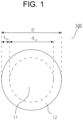
- FIG. 1 illustrates a schematic cross-sectional view (a schematic diagram of a C cross section) of an example of the Al wiring material according to the aspect 1.
- An Al wiring material 100 illustrated in FIG. 1 includes an Al core material 11 as a soft part, and an Al coating layer 12 as a hard part formed on a surface of the Al core material 11.
- the Al core material and the Al coating layer are the same as described above, and the dimensions d 1sc and t 1hc thereof, the Al content, and the diameter D of the Al wiring material are also the same as described above.
- the Vickers hardness is measured on the C cross section of the Al wiring material at regular intervals from the surface side of the Al wiring material toward the center thereof.
- mechanical polishing can be used as a method of exposing the C cross section of the Al wiring material.
- the Vickers hardness is measured at regular intervals on a straight line connecting the surface side to the center.
- the measurement point interval is small in measuring the Vickers hardness, the hardness may be erroneously recognized due to an indentation at an adjacent measurement point.
- the measurement point of the Vickers hardness needs to be determined with a reasonable interval that is assumed from a size of the indentation generated at the time of measurement (that is, a sufficient interval for suppressing erroneous recognition of the hardness due to the indentation at the adjacent measurement point).
- the Vickers hardness may be measured at a point having the following distance from the surface of the Al wiring material for each of the straight lines.
- X represents the number of determined straight lines
- n represents an integral number equal to or larger than 0
- a represents a plot interval ( ⁇ m) of a Vickers hardness profile that is desired to be acquired.
- the number X of the straight lines is appropriately determined so that a value of X ⁇ a becomes a reasonable interval that is assumed from the size of the indentation generated at the time of measurement (that is, a sufficient interval for suppressing erroneous recognition of the hardness due to the indentation at the adjacent measurement point).
- FIG. 4 six straight lines A, B, C, D, E and F the inclinations of which are different from each other by 60° are determined.
- the Vickers hardness is measured at each point at a distance of (6n + 1) ⁇ 3 (um) from the surface such that the distance from the surface of the Al wiring material is 3 ⁇ m, 21 ⁇ m, 39 ⁇ m, 57 um, ...
- the Vickers hardness may be measured at each point at a distance of (6n + 2) ⁇ 3 (um) on the straight line B, at each point at a distance of (6n + 3) ⁇ 3 ( ⁇ m) on the straight line C, at each point at a distance of (6n + 4) ⁇ 3 ( ⁇ m) on the straight line D, at each point at a distance of (6n + 5) ( ⁇ m) on the straight line E, and at each point at a distance of (6n + 6) ⁇ 3 ( ⁇ m) on the straight line F.
- Profiles of the Vickers hardness obtained for the respective straight lines A, B, C, D, E and F are then integrated to form one hardness profile.
- the hardness profile is preferably acquired for three or more C cross sections that are separated from each other by 10 mm or more in a longitudinal direction of the Al wiring material.
- FIG. 5 is an example of the hardness profile of the Al wiring material according to the aspect 1.
- a flat region (plateau region) in which the Vickers hardness shows substantially a constant value is present from the surface of the Al wiring material to a certain depth position (distance). Further advancing toward the center of the Al wiring material, the Vickers hardness is lowered, and thereafter there is a flat region in which the Vickers hardness shows substantially a constant value.
- the "Vickers hardness H 1s (Hv) of the Al core material", the “Vickers hardness H 1h (Hv) of the Al coating layer”, the “thickness t 1hc (um) of the Al coating layer”, and the “diameter d 1sc (um) of the Al core material” of the Al wiring material according to the aspect 1 can be obtained by using a method described in "-Determination of hard part and soft part based on Vickers hardness-" in a column of [Measurement of Vickers hardness] described later based on the obtained hardness profile.
- the Vickers hardness can be adjusted by adjusting/controlling composition of an Al material constituting the Al wiring material, a processing degree and heat treatment of the Al wiring material at the time of manufacture, and the like.
- the Al wiring material includes the Al core material and the Al coating layer formed on the surface of the Al core material, the Al coating layer contains 0.2 to 3 mass%, in total, of one or more element selected from the group consisting of Mg, Sc, Y, Ti, Zr, Hf, V, Nb, Cr, Mo, Mn, Fe, Co, Ni, Cu, Ag, Zn, and Si (hereinafter, also referred to as a "first group element”), and the Al core material contains 0 to 500 mass ppm, in total, of a metallic element of the group 10 of the periodic table of elements (hereinafter, also referred to as a "second group element").
- a metallic element of the group 10 of the periodic table of elements hereinafter, also referred to as a "second group element”
- the Al core material contains 0 to 500 mass ppm, in total, of the second group element encompasses both of a case where the Al core material does not contain the second group element and a case where the Al core material contains the second group element in a range equal to or smaller than 500 mass ppm.
- the Al wiring material having the composition described above may achieve the Al wiring material according to the aspect 1 including the Al core material as the soft part and the Al coating layer as the hard part.
- a preferred range of the diameter d (um) of the Al core material is the same as the preferred range of the diameter d 1sc ( ⁇ m) of the Al core material of the Al wiring material according to the aspect 1 described above.
- the diameter d (um) of the Al core material satisfies a relation of 0.5D ⁇ d ⁇ 0.95D, and more preferably satisfies a relation of 0.52D ⁇ d ⁇ 0.93D, when defining the diameter of the Al wiring material as D ( ⁇ m).
- a preferred range of the thickness t (um) of the Al coating layer is the same as the preferred range of the thickness t 1hc ( ⁇ m) of the Al coating layer of the Al wiring material according to the aspect 1 described above.
- the thickness t ( ⁇ m) of the Al coating layer satisfies a relation of 0.02D ⁇ t ⁇ 0.25D, and more preferably satisfies a relation of 0.03D ⁇ t ⁇ 0.24D, when defining the wire diameter of the Al wiring material as D ( ⁇ m).
- the preferred ranges of the Al content in the Al core material and the Al content in the Al coating layer are the same as described above for the hard part and the soft part. Particularly, from the viewpoint of further achieving effects of the present invention, it is preferable to satisfy a relation of 95 ⁇ x2 ⁇ x1, where x1 is the Al content in the Al core material (mass%) and x2 is the Al content in the Al coating layer (mass%). Preferred conditions for x1 and x2 are the same as described above regarding the Al wiring material according to the aspect 1.
- the Al core material contains 0 to 500 mass ppm of the second group element in total, and the balance of the Al core material consists of Al and inevitable impurities.
- a term of "inevitable impurities" regarding the Al core material encompasses an element constituting the Al coating layer (for example, the first group element).
- the Al coating layer contains 0.2 to 3 mass% of the first group element in total, and the balance of the Al coating layer consists of Al and inevitable impurities.
- a term of "inevitable impurities" regarding the Al coating layer encompasses an element constituting the Al core material (for example, the second group element).
- the first group element contained in the Al coating layer is selected from the group consisting of Mg, Sc, Y, Ti, Zr, Hf, V, Nb, Cr, Mo, Mn, Fe, Co, Ni, Cu, Ag, Zn and Si in combination with the Al core material.
- the Al coating layer more preferably contains one or more element selected from the group consisting of Sc, Zr, Fe, Ni, Cu and Si as the first group element.
- a total concentration (c 1 ) of the first group element in the Al coating layer is preferably equal to or larger than 0.2 mass%, more preferably equal to or larger than 0.4 mass%, and even more preferably equal to or larger than 0.5 mass%, equal to or larger than 0.6 mass%, equal to or larger than 0.8 mass%, or equal to or larger than 1 mass%.
- an upper limit of the total concentration is preferably equal to or smaller than 3 mass%, and more preferably equal to or smaller than 2.8 mass%, equal to or smaller than 2.6 mass%, or equal to or smaller than 2.5 mass%.
- a total concentration (c 2 ) of the second group element in the Al core material is preferably equal to or smaller than 500 mass ppm, and more preferably equal to or smaller than 480 mass ppm, equal to or smaller than 460 mass ppm, equal to or smaller than 450 mass ppm, equal to or smaller than 440 mass ppm, equal to or smaller than 420 mass ppm, or equal to or smaller than 400 mass ppm.
- a lower limit of the total concentration thereof is not particularly limited, and may be 0 mass ppm.
- the Al core material containing the second group element is advantageous because the corrosion resistance of the Al wiring material can be improved.
- the Al core material may contain, as the second group element, one or more of Ni, Pd and Pt, for example, may contain a combination of two elements such as Ni and Pd, Ni and Pt, or Pd and Pt, may contain a combination of three elements including Ni, Pd and Pt, or may contain only one thereof.
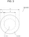
- FIG. 3 illustrates a schematic cross-sectional view (a schematic diagram of the C cross section) of an example of the Al wiring material according to the aspect 1'.
- An Al wiring material 300 illustrated in FIG. 3 includes an Al core material 31 and an Al coating layer 32.
- the Al core material and the Al coating layer are the same as described above, and the dimensions d and t thereof, composition such as the Al content, and the diameter D of the Al wiring material are also the same as described above.
- a concentration analysis focusing on the first group element is performed on the C cross section of the Al wiring material from the surface side of the Al wiring material toward the center.
- an analysis device used for the concentration analysis an energy dispersion-type X-ray analysis (EDS), an electro probe microanalyzer (EPMA), a secondary ion mass spectrometry (SIMS), and the like can be used.
- EDS energy dispersion-type X-ray analysis
- EPMA electro probe microanalyzer
- SIMS secondary ion mass spectrometry
- concentration profiles for three or more C cross sections separated from each other by 10 mm or more in the longitudinal direction of the Al wiring material it is preferable to acquire concentration profiles for three or more C cross sections separated from each other by 10 mm or more in the longitudinal direction of the Al wiring material.
- the "total concentration c 1 (mass%) of the first group element in the Al coating layer", the "diameter d ( ⁇ m) of the Al core material", and the “thickness t ( ⁇ m) of the Al coating layer” of the Al wiring material according to the aspect 1' can be obtained by using a method described in "-Determination of Al core material and Al coating layer based on total concentration c 1 of first group element-" in a column of [Measurement of element content] described later based on the obtained concentration profile.
- total concentration c 2 (mass ppm) of the second group element in the Al core material can be measured by using a method described in "-Measurement of total concentration c 2 of second group element-" in the column of [Measurement of element content] described later.
- the Al wiring material according to the aspect 2 includes the Al core material as the hard part, and the Al coating layer as the soft part formed on the surface of the Al core material.
- the Al wiring material according to the aspect 2 includes the soft Al coating layer on the surface thereof, so that softness of the loop rising part in the vicinity of the connection part can be secured.
- generation of a heel crack can be reduced under the environment at the time when the device operates.
- Due to the soft Al coating layer a chip damage can be suppressed at the time of connection to the member to be connected.
- the development of the crack can be reduced at the time when the crack reaches the hard Al core material.
- the hard part and the soft part are the same as described above. From the viewpoint that both of suppression of a chip damage and thermal shock resistance can be achieved at a high level, it is preferable to satisfy 1.2 ⁇ H 2h /H 2s where that H 2h is the Vickers hardness of the Al core material (Hv) and H 2s is the Vickers hardness of the Al coating layer (Hv). A more preferred range of H 2h /H 2s is the same as described above regarding H h /H s .
- the diameter d 2hc (um) of the Al core material is preferably equal to or larger than 0.25D, more preferably equal to or larger than 0.3D, and even more preferably equal to or larger than 0.32D, equal to or larger than 0.34D, or equal to or larger than 0.35D, when defining the diameter of the Al wiring material as D ( ⁇ m).
- an upper limit of the diameter d 2hc ( ⁇ m) is preferably equal to or smaller than 0.7D, more preferably equal to or smaller than 0.65D, and even more preferably equal to or smaller than 0.64D, equal to or smaller than 0.62D, or equal to or smaller than 0.6D.
- the diameter d 2hc ( ⁇ m) of the Al core material be equal to or larger than 0.3D and equal to or smaller than 0.65D because there can be achieved the Al wiring material that may suppress a chip damage and is excellent in thermal shock resistance.
- the diameter d 2hc ( ⁇ m) of the Al core material satisfies a relation of 0.25D ⁇ d 2hc ⁇ 0.7D, and more preferably satisfies a relation of 0.3D ⁇ d 2hc ⁇ 0.65D, when defining the diameter of the Al wiring material as D ( ⁇ m).
- the thickness t 2sc ( ⁇ m) of the Al coating layer is preferably equal to or larger than 0.16D, more preferably equal to or larger than 0.18D, and even more preferably equal to or larger than 0.2D, when defining the diameter of the Al wiring material as D ( ⁇ m).
- an upper limit of the thickness t 2sc ( ⁇ m) is preferably equal to or smaller than 0.37D, more preferably equal to or smaller than 0.35D, and even more preferably equal to or smaller than 0.34D, equal to or smaller than 0.32D, or equal to or smaller than 0.3D.
- the thickness t 2sc ( ⁇ m) of the Al coating layer be equal to or larger than 0.18D and equal to or smaller than 0.35D because there can be achieved the Al wiring material that may suppress a chip damage and is excellent in thermal shock resistance.
- the thickness t 2sc ( ⁇ m) of the Al coating layer satisfies a relation of 0.16D ⁇ t 2sc ⁇ 0.37D, and more preferably satisfies a relation of 0.18D ⁇ t 2sc 0.35D, when defining the diameter of the Al wiring material as D ( ⁇ m) .
- the preferred ranges of the Al content in the hard part (Al core material) and the Al content in the soft part (Al coating layer) are the same as described above. Particularly, from the viewpoint of further achieving effects of the present invention, it is preferable to satisfy a relation of 95 ⁇ y1 ⁇ y2, where y1 is the Al content in the Al core material (mass%) and y2 is the Al content in the Al coating layer (mass%). y1 and y2 more preferably satisfies a relation of 96 ⁇ y1 ⁇ y2, and even more preferably satisfies a relation of 96.5 ⁇ y1 ⁇ y2.
- y2 preferably satisfies a condition of 99.5 ⁇ y2, more preferably satisfies a condition of 99.6 ⁇ y2, and even more preferably satisfies a condition of 99.8 ⁇ y2.
- the upper limit of y2 may be 99.9999 (mass%) as described above, for example.
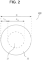
- FIG. 2 illustrates a schematic cross-sectional view (a schematic diagram of a C cross section) of an example of the Al wiring material according to the aspect 2.
- An Al wiring material 200 illustrated in FIG. 2 includes an Al core material 21 as the hard part, and an Al coating layer 22 as the soft part formed on the surface of the core material 21.
- the Al core material and the Al coating layer are the same as described above, and the dimensions d 2hc and t 2sc thereof, the Al content, and the diameter D of the Al wiring material are also the same as described above.
- the Vickers hardness is measured.
- the Vickers hardness can be measured by using the same method as described above regarding the Al wiring material according to the aspect 1.
- the "Vickers hardness H 2s (Hv) of the Al coating layer", the “Vickers hardness H 2h (Hv) of the Al core material”, the “thickness t 2sc (um) of the Al coating layer”, and the “diameter d 2hc (um) of the Al core material” of the Al wiring material according to the aspect 2 can be obtained by using a method described in "-Determination of hard part and soft part based on Vickers hardness-" in a column of [Measurement of Vickers hardness] described later based on the obtained hardness profile.
- the Al wiring material includes the Al core material and the Al coating layer formed on the surface of the Al core material
- the Al core material contains 0.2 to 3 mass%, in total, of one or more element selected from the group consisting of Mg, Sc, Y, Ti, Zr, Hf, V, Nb, Cr, Mo, Mn, Fe, Co, Ni, Cu, Ag, Zn and Si
- first group element Mg, Sc, Y, Ti, Zr, Hf, V, Nb, Cr, Mo, Mn, Fe, Co, Ni, Cu, Ag, Zn and Si
- the Al coating layer contains 0 to 500 mass ppm, in total, of a metallic element of the group 10 of the periodic table of elements ("second group element").
- second group element such an embodiment is also referred to as an "aspect 2'".
- the Al coating layer contains 0 to 500 mass ppm, in total, of the second group element encompasses both of a case where the Al coating layer does not contain the second group element and a case where the Al coating layer contains the second group element in a range equal to or smaller than 500 mass ppm.
- the Al wiring material having the composition described above may achieve the Al wiring material according to the aspect 2 including the Al core material as the hard part and the Al coating layer as the soft part.
- a preferred range of the diameter d ( ⁇ m) of the Al core material is the same as the preferred range of the diameter d 2hc ( ⁇ m) of the Al core material of the Al wiring material according to the aspect 2 described above.
- the diameter d ( ⁇ m) of the Al core material satisfies a relation of 0.25D ⁇ d ⁇ 0.7D, and more preferably satisfies a relation of 0.3D ⁇ d ⁇ 0.65D, when defining the diameter of the Al wiring material as D ( ⁇ m).
- a preferred range of the thickness t (um) of the Al coating layer is the same as the preferred range of the thickness t 2sc ( ⁇ m) of the Al coating layer of the Al wiring material according to the aspect 2 described above.
- the thickness t ( ⁇ m) of the Al coating layer satisfies a relation of 0.16D ⁇ t ⁇ 0.37D, and more preferably satisfies a relation of 0.18D ⁇ t ⁇ 0.35D, when defining the diameter of the Al wiring material as D ( ⁇ m).
- the preferred ranges of the Al content in the Al core material and the Al content in the Al coating layer are the same as described above for the hard part and the soft part. Particularly, from the viewpoint of further achieving effects of the present invention, it is preferable to satisfy a relation of 95 ⁇ y1 ⁇ y2, where y1 is the Al content in the Al core material (mass%) and y2 is the Al content in the Al coating layer (mass%). Preferred conditions for y1 and y2 are the same as described above regarding the Al wiring material according to the aspect 2.
- the Al core material contains 0.2 to 3 mass% of the first group element in total, and the balance of the Al core material consists of Al and inevitable impurities.
- a term of "inevitable impurities" regarding the Al core material encompasses an element constituting the Al coating layer (for example, the second group element).
- the Al coating layer contains 0 to 500 mass ppm of the second group element in total, and the balance of the Al coating layer consists of Al and inevitable impurities.
- a term of "inevitable impurities" regarding the Al coating layer encompasses an element constituting the Al core material (for example, the first group element).
- the first group element contained in the Al core material is selected from the group consisting of Mg, Sc, Y, Ti, Zr, Hf, V, Nb, Cr, Mo, Mn, Fe, Co, Ni, Cu, Ag, Zn and Si in combination with the Al coating layer.
- the Al core material more preferably contains one or more element selected from the group consisting of Sc, Zr, Fe, Ni, Cu and Si as the first group element.
- a total concentration (c 1 ) of the first group element in the Al core material is preferably equal to or larger than 0.2 mass%, more preferably equal to or larger than 0.4 mass%, and even more preferably equal to or larger than 0.5 mass%, equal to or larger than 0.6 mass%, equal to or larger than 0.8 mass%, or equal to or larger than 1 mass%.
- an upper limit of the total concentration thereof is preferably equal to or smaller than 3 mass%, and more preferably equal to or smaller than 2.8 mass%, equal to or smaller than 2.6 mass%, or equal to or smaller than 2.5 mass%.
- a total concentration (c 2 ) of the second group element in the Al coating layer is preferably equal to or smaller than 500 mass ppm, and more preferably equal to or smaller than 480 mass ppm, equal to or smaller than 460 mass ppm, equal to or smaller than 450 mass ppm, equal to or smaller than 440 mass ppm, equal to or smaller than 420 mass ppm, or equal to or smaller than 400 mass ppm.
- a lower limit of the total concentration thereof is not particularly limited, and may be 0 mass ppm.
- the Al coating layer containing the second group element is advantageous because a corrosion resistance of the Al wiring material can be improved.
- the Al coating layer may contain, as the second group element, one or more of Ni, Pd and Pt, for example, may contain a combination of two elements such as Ni and Pd, Ni and Pt, or Pd and Pt, may contain a combination of three elements including Ni, Pd and Pt, or may contain only one thereof.
- FIG. 3 illustrates a schematic cross-sectional view (a schematic diagram of the C cross section) of an example of the Al wiring material according to the aspect 2'.
- An Al wiring material 400 illustrated in FIG. 3 includes an Al core material 41 and an Al coating layer 42.
- the Al core material and the Al coating layer are the same as described above, and the dimensions d and t thereof, composition such as the Al content, and the diameter D of the Al wiring material are also the same as described above.
- a concentration analysis is performed focusing on the first group element.
- the concentration analysis can be performed by using the same method as described above regarding the Al wiring material according to the aspect 1'.
- the "total concentration c 1 (mass%) of the first group element in the Al core material", the “diameter d (um) of the Al core material”, and the “thickness t ( ⁇ m) of the Al coating layer” of the Al wiring material according to the aspect 2' can be obtained by using a method described in "-Determination of Al core material and Al coating layer based on total concentration c 1 of first group element-" in a column of [Measurement of element content] described later based on the obtained concentration profile.
- total concentration c 2 (mass ppm) of the second group element in the Al coating layer can be measured by using a method described in "-Measurement of total concentration c2 of second group element-" in the column of [Measurement of element content] described later.
- a method for manufacturing the Al wiring material according to the present invention is not particularly limited so long as the Al wiring material including the hard part and the soft part can be manufactured. There will be described an example of manufacturing an Al bonding wire.
- an Al raw material Al raw material having purity of 4N or more
- an additive element raw material are weighed as starting materials, and melted and mixed to obtain an ingot that contains predetermined components with the balance consisting of Al and inevitable impurities.
- a mother alloy containing the additive element in high concentration may be used as the raw material for each additive element.
- This ingot is subjected to wire-drawing using dies to have a finally required diameter of the Al core material.
- extrusion processing can be performed for a large diameter.
- a method for forming the Al coating layer on the surface of the Al core material As a method for forming the Al coating layer on the surface of the Al core material, a vapor deposition method, a cladding method, a composite extrusion method, and the like can be used.
- a stage of compositing/attaching the Al coating layer on the surface of the Al core material is not particularly limited, and may be performed before wire-drawing processing for the Al core material (for example, a stage of extrusion molding the ingot for the core material), may be performed in the middle of the wire-drawing processing for the Al core material, or may be performed after the Al core material is subjected to the wire-drawing to have a final diameter.
- the Al wiring material according to the present invention may be manufactured by: extrusion-molding the ingot for the core material in a columnar shape; extrusion-molding the ingot for the coating layer in a cylindrical shape; combining them with each other to be subjected to composite-extrusion processing to make a composite wire rod having a columnar shape; and performing wire-drawing processing thereon to have the final diameter.
- a solution heat treatment may be performed in a state of the ingot, in the middle of processing or after the processing end.
- the solution heat treatment may be separately performed especially at a stage before compositing/attaching the Al core material and the Al coating layer.
- the additive elements are dissolved in Al at a high temperature at which the solid solubility is high. Then, the resultant is cooled to an ordinary temperature at increased cooling rate by water cooling, air cooling, or the like in order to suppress the precipitation of the dissolved elements.
- the solution heat treatment may be performed, for example, by heating at a temperature range of 500 to 640°C for 0.5 hours to 3 hours, followed by cooling with water cooling, air cooling, or the like.
- the solution heat treatment is performed in a range under a condition for which a difference between the soft part and the hard part does not become unclear due to diffusion in the obtained Al wiring material.
- an aging heat treatment may be performed after the solution heat treatment.
- the aging heat treatment may be separately performed especially at a stage before compositing/attaching the Al core material and the Al coating layer.
- a state of solid solution and precipitation of a dopant such as the first group element can be controlled, and the hardness of the Al wiring material can thus be controlled.
- the aging heat treatment may be performed, for example, at a temperature range of 200 to 400°C for 0.5 hours to 12 hours.
- the aging heat treatment is performed after the Al core material and the Al coating layer are composited with/attached to each other, the aging heat treatment is performed in a range under a condition for which a difference between the soft part and the hard part does not become unclear due to diffusion in the obtained Al wiring material.
- the Al wiring material may be subjected to a thermal refining heat treatment.
- the thermal refining heat treatment By performing the thermal refining heat treatment, the working strain is removed, a recrystallized structure is formed, and a precipitate can be formed.
- this thermal refining heat treatment it is preferable that the heat treatment be continuously performed while the Al wiring material is continuously swept in a heating furnace. Examples of this heat treatment condition may include heating at a temperature range of 200 to 600°C for a short time of 1 second to 2 minutes.
- the thermal refining heat treatment can simultaneously serve also as the precipitation heat treatment depending on a necessary degree of precipitation.
- Semiconductor devices can be manufactured by connecting the electrode on the semiconductor chip to the lead frame or an electrode on a circuit board by using the Al wiring material of the present invention.
- the semiconductor device of the present invention includes the Al wiring material of the present invention.
- the Al wiring material according to the present invention achieves both of suppression of a chip damage and thermal shock resistance.
- the semiconductor device including the Al wiring material may achieve excellent operation reliability even in a case where a significant temperature change is caused in accordance with the operation cycle of the device.
- the semiconductor device of the present invention includes the circuit board, the semiconductor chip, and the Al wiring material for bringing the circuit board and the semiconductor chip into conduction with each other, and is characterized in that the Al wiring material is the Al wiring material of the present invention.
- the circuit board and the semiconductor chip are not particularly limited, and a known circuit board and semiconductor chip that may be used for constituting the semiconductor device may be used.
- a lead frame may be used in place of the circuit board.
- the semiconductor device may include a lead frame and a semiconductor chip mounted on the lead frame.
- Examples of the semiconductor device include various semiconductor devices used for electric products (for example, a computer, a cellular telephone, a digital camera, a television, an air conditioner, a solar power generation system), vehicles (for example, a motorcycle, an automobile, an electric train, a ship, and an aircraft), and the like, and a semiconductor device for electric power (power semiconductor device) is especially preferred.
- various semiconductor devices used for electric products for example, a computer, a cellular telephone, a digital camera, a television, an air conditioner, a solar power generation system
- vehicles for example, a motorcycle, an automobile, an electric train, a ship, and an aircraft
- a semiconductor device for electric power power semiconductor device
- a method for producing a sample will be described.
- Al having a purity of 99.99 mass% or more with the balance consisting of inevitable impurities was used.
- the first group element Mg, Sc, Y, Ti, Zr, Hf, V, Nb, Cr, Mo, Mn, Fe, Co, Ni, Cu, Ag, Zn, Si
- the second group element Ni, Pd, Pt
- elements having a purity of 99 mass% or more with the balance consisting of inevitable impurities were used. Ingots were casted by compounding and melting these raw materials so that the composition of the Al core material indicated in Table 1 and Table 2 can be obtained.
- the ingot for the coating layer was extrusion-molded in a cylindrical shape and the ingot for the core material was extrusion-molded in a columnar shape to have predetermined coating layer thickness and core material diameter. Subsequently, by combining them to be subjected to composite-extrusion processing, a columnar composite wire rod having a diameter of 9.5 mm was produced. Regarding some of the samples, after performing the solution heat treatment and the aging heat treatment for the purpose of final hardness adjustment separately at a stage before compositing the wire material, a columnar composite wire rod was produced. The solution heat treatment was performed by heating at a temperature range of 550 to 620°C for 0.5 hours to 1 hour, followed by cooling with water cooling.
- the aging heat treatment was performed by heating at a temperature range of 250 to 350°C for 0.5 hours to 3 hours after the solution heat treatment.
- the obtained columnar composite wire rod was subjected to the wire-drawing processing with dies to have the final diameter of 300 ⁇ m.
- the thermal refining heat treatment was performed with a diameter of (1) 0.9 to 1.1 mm, (2) 450 to 550 um, and (3) 300 ⁇ m (final diameter) so that predetermined mechanical characteristic and Vickers hardness can be obtained.
- the thermal refining heat treatment was performed at a processing temperature of 450 to 600°C for a processing time equal to or longer than 5 seconds and shorter than 1 minute in an Ar atmosphere.
- the Vickers hardness of the Al wiring material was measured by using a micro Vickers hardness tester ("HM-200" manufactured by Mitutoyo Corporation).
- HM-200 micro Vickers hardness tester
- the six straight lines A, B, C, D, E and F the inclinations of which were different from each other by 60° were determined, and the Vickers hardness was measured at each point at a distance of (6n + 1) ⁇ 3 ( ⁇ m) (herein, n represents an integral number equal to or larger than 0. The same applies hereinafter.) from the surface of the Al wiring material on the straight line A.
- the Vickers hardness was also measured at each point at a distance of (6n + 2) ⁇ 3 ( ⁇ m) on the straight line B, at each point at a distance of (6n + 3) ⁇ 3 ( ⁇ m) on the straight line C, at each point at a distance of (6n + 4) ⁇ 3 ( ⁇ m) on the straight line D, at each point at a distance of (6n + 5) ⁇ 3 ( ⁇ m) on the straight line E, and at each point at a distance of (6n + 6) ⁇ 3 on the straight line F. Profiles of the Vickers hardness obtained for the respective straight lines A, B, C, D, E and F were then integrated to form one hardness profile.
- the hardness profile indicating the information of the Vickers hardness at intervals of 3 ⁇ m from the surface of the Al wiring material toward the center was obtained.
- the measurement described above was performed for three C cross sections separated from each other by 10 mm or more in the longitudinal direction of the Al wiring material, and the hardness profile was obtained (the number of hardness profiles for each sample was three).
- the interval for obtaining the information of the Vickers hardness was appropriately changed such that the information of the Vickers hardness was obtained at smaller intervals (2 ⁇ m and the like) in a case where the Al coating layer was thin, and thus the flat region (plateau region) on the surface side of the Al wiring material was thin in the obtained hardness profile.
- the Vickers hardness of the Al core material, the Vickers hardness of the Al coating layer, the diameter of the Al core material, and the thickness of the Al coating layer were obtained in accordance with the procedure described above.
- An average value of the Vickers hardness of the Al core material obtained in the three hardness profiles is indicated in a column of "Hardness H 1s (Hv)" in Table 2 as the "Vickers hardness H 1s (Hv) of the Al core material".
- an average value of the Vickers hardness of the Al coating layer is indicated as the "Vickers hardness H 1h (Hv) of the Al coating layer”
- an average value of the thickness of the Al coating layer is indicated as the “thickness t 1hc (um) of the Al coating layer”
- an average value of the diameter of the Al core material is indicated as the “diameter d 1sc (um) of the Al core material” in columns of "hardness H 1h (Hv)", “thickness t 1hc (pm)", and "diameter d 1sc ( ⁇ m)” in Table 2, respectively.
- the Vickers hardness of the hard part (Al core material) was obtained by three-point averaging the Vickers hardness of the flat region (plateau region) on the center side of the Al wiring material in the obtained hardness profile.
- the Vickers hardness of the soft part (Al coating layer) was obtained by three-point averaging the Vickers hardness of the flat region (plateau region) on the surface side of the Al wiring material in the obtained hardness profile.
- a position where the Vickers hardness is equal to [(Vickers hardness of the Al core material) + (Vickers hardness of the Al coating layer)]/2 was determined to be a boundary between the Al core material and the Al coating layer, and a distance from the boundary to the surface was determined to be the thickness (um) of the Al coating layer.
- the wire diameter ( ⁇ m) of the Al core material was obtained based on an expression: (the diameter of the Al wiring material) - 2 ⁇ (the thickness of the Al coating layer).
- the Vickers hardness of the Al core material, the Vickers hardness of the Al coating layer, the diameter of the Al core material, and the thickness of the Al coating layer were obtained in accordance with the procedure described above. Average values of the respective values obtained in the three hardness profiles are indicated as the "Vickers hardness H 2h (Hv) of the Al core material", the “Vickers hardness H 2s (Hv) of the Al coating layer", the “thickness t 2sc ( ⁇ m) of the Al coating layer ", and the "diameter d 2hc ( ⁇ m) of the Al core material” in columns of "hardness H 2h (Hv)", “hardness H 2s (Hv)", “thickness t 2sc ( ⁇ m)", and “diameter d 2hc ( ⁇ m)” in Table 2, respectively.
- the contents of Al and the first group element in the Al wiring material were measured by using an electro probe microanalyzer (EPMA).
- EPMA electro probe microanalyzer
- For the C cross section of the Al wiring material by determining a straight line passing from the surface of the Al wiring material through the center like the straight line A illustrated in FIG. 4 , and performing linear analysis for the straight line (measurement interval is 0.3 to 1.0 ⁇ m), a concentration profile of each element of the first group element and Al was obtained from the surface of the Al wiring material toward the center. Concentration profiles of the respective elements of first group elements were added together to form a profile related to a total concentration of the first group elements (hereinafter, also referred to as a "total concentration profile of the first group elements").
- the concentration profile indicating the information of the total concentration of the first group elements at predetermined intervals from the surface of the Al wiring material toward the center was obtained.
- the measurement described above was performed for three C cross sections separated from each other by 10 mm or more in the longitudinal direction of the Al wiring material, and the concentration profile was obtained (the number of concentration profiles for each sample was three).
- the total concentration c of the first group elements in the Al coating layer, the diameter of the Al core material, and the thickness of the Al coating layer were obtained in accordance with the procedure described above. Average values of the respective values obtained in the three concentration profiles are indicated as the “total concentration c 1 (mass%) of the first group elements in the Al coating layer", the “diameter d ( ⁇ m) of the Al core material", and the “thickness t ( ⁇ m) of the Al coating layer", respectively.
- the Al wiring material according to the aspect 1' contains Ni as the first group element in the Al coating layer and contains Ni as the second group element in the Al core material, that is, a case where Ni is contained in both of the Al coating layer and the Al core material (examples of the present invention 1-20, 1-36). Also in this case, it was confirmed that the diameter of the Al core material and the thickness of the Al coating layer could be properly obtained by using the determination method described above (determining that the position of 0.5c is the boundary) focusing on the total concentration c of the first group elements in the Al coating layer.
- the diameter d ( ⁇ m) of the Al core material and the thickness t ( ⁇ m) of the Al coating layer obtained by using the determination method described above focusing on the total concentration c of the first group elements in the Al coating layer were substantially the same as the diameter d 1sc ( ⁇ m) of the Al core material and the thickness t 1hc ( ⁇ m) of the Al coating layer that were obtained based on the hardness profile.
- the total concentration c (mass%) of the first group elements in the Al core material was obtained by three-point averaging the total concentration of the first group elements in a flat region in the vicinity of the center of the Al wiring material in which a concentration gradient is small in the obtained total concentration profile of the first group elements.
- concentration profile a position where the total concentration of the first group elements is 0.5c (mass%) was determined to be a boundary between the Al coating layer and the Al core material, and a distance from the boundary to the surface was determined to be the thickness (um) of the Al coating layer.
- the diameter ( ⁇ m) of the Al core material was obtained based on an expression: (the diameter of the Al wiring material) - 2 ⁇ (the thickness of the Al coating layer).
- the total concentration c of the first group elements in the Al core material, the diameter of the Al core material, and the thickness of the Al coating layer were obtained in accordance with the procedure described above. Average values of the respective values obtained in the three concentration profiles are indicated as the “total concentration c 1 (mass%) of the first group elements in the Al core material", the “diameter d ( ⁇ m) of the Al core material", and the “thickness t ( ⁇ m) of the Al coating layer", respectively.
- the Al wiring material according to the aspect 2' contains Ni as the first group element in the Al core material and contains Ni as the second group element in the Al coating layer, that is, a case where Ni is contained in both of the Al core material and the Al coating layer (example of the present invention 2-5). Also in this case, it was confirmed that the diameter of the Al core material and the thickness of the Al coating layer could be properly obtained by using the determination method described above (determining that the position of 0.5c is the boundary) focusing on the total concentration c of the first group elements in the Al core material.
- the diameter d ( ⁇ m) of the Al core material and the thickness t (um) of the Al coating layer obtained by using the determination method described above focusing on the total concentration c of the first group elements in the Al core material were substantially the same as the diameter d 2hc ( ⁇ m) of the Al core material and the thickness t 2sc ( ⁇ m) of the Al coating layer that were obtained based on the hardness profile.
- the content of the second group element in the Al wiring material was measured as follows using laser ablation ICP mass spectrometry (LA-ICP-MS).
- an electrode on the semiconductor chip was an Al-Cu pad, and Ag was used for an external terminal.
- a first connection part between the electrode on the semiconductor chip and the Al wiring material, and a second connection part between the external terminal and the Al wiring material were both wedge-bonded.
- N the number of evaluations
- a case in which a crack, traces of bonding, and the like were not found was determined to be favorable to be marked with a symbol of "double circle”
- a case in which there was no crack but traces of bonding were found at some spots (three spots or less of the number of evaluations 50) was marked with a symbol of "circle”
- the other cases were marked with a symbol of "cross”.
- Thermal shock resistance was evaluated by a power cycle test.
- heating and cooling were alternately and repeatedly performed for the semiconductor device to which the Al wiring material was connected. Heating was performed for 2 seconds until the temperature of the connection part of the Al wiring material in the semiconductor device reached 120°C, and cooling was performed for 20 seconds until the temperature of the connection part reached 30°C. This heating/cooling cycle was repeated 100000 times.
- connection part reliability was evaluated.
- the shear force was measured as comparison with shear force of the connection part at an initial stage (before the power cycle test).
- a strength equal to or larger than 90% of the connection strength at the initial stage is marked with a symbol of "double circle”
- a strength equal to or larger than 80% thereof is marked with a symbol of "circle”
- a strength equal to or larger than 60% thereof is marked with a symbol of "triangle”
- a strength smaller than 60% thereof is marked with a symbol of "cross”.
- the configuration of the Al wiring material and evaluation results are shown in Tables 1 and 2.
- the examples shown in Table 1 are related to the Al wiring material including the Al core material as the soft part and the Al coating layer as the hard part
- the examples shown in Table 2 are related to the Al wiring material including the Al core material as the hard part and the Al coating layer as the soft part.
Landscapes
- Chemical & Material Sciences (AREA)
- Engineering & Computer Science (AREA)
- Organic Chemistry (AREA)
- Materials Engineering (AREA)
- Mechanical Engineering (AREA)
- Metallurgy (AREA)
- Crystallography & Structural Chemistry (AREA)
- Thermal Sciences (AREA)
- Physics & Mathematics (AREA)
- Conductive Materials (AREA)
- Computer Hardware Design (AREA)
- Microelectronics & Electronic Packaging (AREA)
- Power Engineering (AREA)
- Internal Circuitry In Semiconductor Integrated Circuit Devices (AREA)
- Non-Insulated Conductors (AREA)
- Parts Printed On Printed Circuit Boards (AREA)
Applications Claiming Priority (2)
| Application Number | Priority Date | Filing Date | Title |
|---|---|---|---|
| JP2021017609 | 2021-02-05 | ||
| PCT/JP2022/003580 WO2022168788A1 (fr) | 2021-02-05 | 2022-01-31 | Matériau de câblage d'al |
Publications (2)
| Publication Number | Publication Date |
|---|---|
| EP4289984A1 true EP4289984A1 (fr) | 2023-12-13 |
| EP4289984A4 EP4289984A4 (fr) | 2025-06-18 |
Family
ID=82741404
Family Applications (1)
| Application Number | Title | Priority Date | Filing Date |
|---|---|---|---|
| EP22749660.1A Pending EP4289984A4 (fr) | 2021-02-05 | 2022-01-31 | Matériau de câblage d'al |
Country Status (6)
| Country | Link |
|---|---|
| US (1) | US20240105668A1 (fr) |
| EP (1) | EP4289984A4 (fr) |
| JP (1) | JP7793554B2 (fr) |
| CN (1) | CN116918050A (fr) |
| TW (1) | TW202239984A (fr) |
| WO (1) | WO2022168788A1 (fr) |
Families Citing this family (1)
| Publication number | Priority date | Publication date | Assignee | Title |
|---|---|---|---|---|
| WO2025115915A1 (fr) * | 2023-11-27 | 2025-06-05 | 日鉄ケミカル&マテリアル株式会社 | Fil de liaison d'al ou ruban de liaison d'al |
Family Cites Families (13)
| Publication number | Priority date | Publication date | Assignee | Title |
|---|---|---|---|---|
| JPS6118163A (ja) * | 1984-07-04 | 1986-01-27 | Hitachi Cable Ltd | ボンデイングワイヤ |
| EP0241721B1 (fr) * | 1986-03-18 | 1992-09-23 | Sumitomo Electric Industries, Ltd. | Conducteur et son procédé de production |
| JPH0766236A (ja) * | 1993-08-31 | 1995-03-10 | Tanaka Denshi Kogyo Kk | 半導体素子用多層被覆ボンディングワイヤ及び半導体装置 |
| JP2002246542A (ja) | 2001-02-15 | 2002-08-30 | Matsushita Electric Ind Co Ltd | パワーモジュール及びその製造方法 |
| JP4465906B2 (ja) | 2001-04-18 | 2010-05-26 | 株式会社日立製作所 | パワー半導体モジュール |
| JP4988243B2 (ja) * | 2005-04-28 | 2012-08-01 | 昭和電工株式会社 | プリント配線基板 |
| WO2013030968A1 (fr) * | 2011-08-31 | 2013-03-07 | 田中電子工業株式会社 | Ruban de cuivre rectangulaire revêtu d'aluminium, d'or, de palladium ou de platine pour élément semi-conducteur |
| EP2736047B1 (fr) | 2012-11-22 | 2017-11-08 | Heraeus Deutschland GmbH & Co. KG | Fil d'alliage d'aluminium pour applications de liaison |
| JP5680138B2 (ja) * | 2013-05-15 | 2015-03-04 | 田中電子工業株式会社 | 耐食性アルミニウム合金ボンディングワイヤ |
| JP6534809B2 (ja) * | 2014-12-05 | 2019-06-26 | 古河電気工業株式会社 | アルミニウム合金線材、アルミニウム合金撚線、被覆電線、ワイヤーハーネス、並びにアルミニウム合金線材およびアルミニウム合金撚線の製造方法 |
| JP2016152316A (ja) | 2015-02-17 | 2016-08-22 | 住友金属鉱山株式会社 | ボンディング用アルミニウム配線材及び電子部品 |
| JP6430080B1 (ja) * | 2017-03-27 | 2018-11-28 | 古河電気工業株式会社 | アルミニウム合金材並びにこれを用いた導電部材、導電部品、バネ用部材、バネ用部品、半導体モジュール用部材、半導体モジュール用部品、構造用部材及び構造用部品 |
| CN114654828B (zh) * | 2017-04-24 | 2024-08-06 | 诺维尔里斯公司 | 包覆铝合金产品和其制备方法 |
-
2022
- 2022-01-31 US US18/275,584 patent/US20240105668A1/en active Pending
- 2022-01-31 WO PCT/JP2022/003580 patent/WO2022168788A1/fr not_active Ceased
- 2022-01-31 CN CN202280013331.1A patent/CN116918050A/zh active Pending
- 2022-01-31 EP EP22749660.1A patent/EP4289984A4/fr active Pending
- 2022-01-31 JP JP2022579525A patent/JP7793554B2/ja active Active
- 2022-02-07 TW TW111104291A patent/TW202239984A/zh unknown
Also Published As
| Publication number | Publication date |
|---|---|
| JPWO2022168788A1 (fr) | 2022-08-11 |
| US20240105668A1 (en) | 2024-03-28 |
| EP4289984A4 (fr) | 2025-06-18 |
| TW202239984A (zh) | 2022-10-16 |
| CN116918050A (zh) | 2023-10-20 |
| WO2022168788A1 (fr) | 2022-08-11 |
| JP7793554B2 (ja) | 2026-01-05 |
Similar Documents
| Publication | Publication Date | Title |
|---|---|---|
| JP4516154B1 (ja) | Cu−Mg−P系銅合金条材及びその製造方法 | |
| EP2298945B1 (fr) | Matériau de tôle d alliage de cuivre et procédé de fabrication de celui-ci | |
| JP4563508B1 (ja) | Cu−Mg−P系銅合金条材及びその製造方法 | |
| KR101136265B1 (ko) | 전기 전자 부품용 구리 합금판 | |
| EP3438299A1 (fr) | Alliage de cuivre pour matériel électronique et électrique, bande de tôle en alliage de cuivre pour matériel électronique et électrique, composant pour matériel électronique et électrique, borne, barre omnibus et pièce mobile pour des relais | |
| EP3020838A1 (fr) | Alliage de cuivre pour équipement électronique et électrique, feuille mince d'alliage de cuivre pour équipement électronique et électrique, et composants conducteurs pour équipement électronique et électrique, terminal | |
| EP2333127A1 (fr) | Matière d'alliage de cuivre pour un composant électrique/électronique | |
| EP4534709A1 (fr) | Fil de liaison en alliage d'al | |
| EP4289983A1 (fr) | Fil de liaison en al pour dispositifs à semi-conducteur | |
| EP4289984A1 (fr) | Matériau de câblage d'al | |
| EP4289986A1 (fr) | Fil de liaison en al pour dispositifs à semi-conducteur | |
| JP6162512B2 (ja) | 二次電池集電体用銅合金圧延箔およびその製造方法 | |
| JP6182372B2 (ja) | 二次電池集電体用銅合金圧延箔およびその製造方法 | |
| JP6927844B2 (ja) | 銅合金板材およびその製造方法 | |
| EP4040448A1 (fr) | Matériau de câblage en al | |
| JP6190646B2 (ja) | 二次電池集電体用銅合金圧延箔およびその製造方法 | |
| JP2013142162A (ja) | 反り付け加工性に優れたベース板用銅或いは銅合金板及びその製造方法 | |
| JP7795484B2 (ja) | Al配線材 | |
| EP4474506A1 (fr) | Alliage de cuivre pour matériau électronique, et composant électronique | |
| KR101807969B1 (ko) | 전자 부품용 Cu-Co-Ni-Si 합금 | |
| US20070131321A1 (en) | Copper alloy for electric and electronic instruments | |
| EP3643798A1 (fr) | Titane-cuivre, procédé de production de titane-cuivre et composant électronique | |
| KR102343189B1 (ko) | 절연 기판 및 그 제조 방법 | |
| JP2000080426A (ja) | 電子機器用銅合金 | |
| JP2025096791A (ja) | 銀合金線及びこれを用いた導電線、接合用線、半導体用線並びに構造用線 |
Legal Events
| Date | Code | Title | Description |
|---|---|---|---|
| STAA | Information on the status of an ep patent application or granted ep patent |
Free format text: STATUS: THE INTERNATIONAL PUBLICATION HAS BEEN MADE |
|
| PUAI | Public reference made under article 153(3) epc to a published international application that has entered the european phase |
Free format text: ORIGINAL CODE: 0009012 |
|
| STAA | Information on the status of an ep patent application or granted ep patent |
Free format text: STATUS: REQUEST FOR EXAMINATION WAS MADE |
|
| 17P | Request for examination filed |
Effective date: 20230831 |
|
| AK | Designated contracting states |
Kind code of ref document: A1 Designated state(s): AL AT BE BG CH CY CZ DE DK EE ES FI FR GB GR HR HU IE IS IT LI LT LU LV MC MK MT NL NO PL PT RO RS SE SI SK SM TR |
|
| DAV | Request for validation of the european patent (deleted) | ||
| DAX | Request for extension of the european patent (deleted) | ||
| REG | Reference to a national code |
Ref country code: DE Ref legal event code: R079 Free format text: PREVIOUS MAIN CLASS: C22C0021000000 Ipc: H01L0023480000 |
|
| RIC1 | Information provided on ipc code assigned before grant |
Ipc: H01L 21/60 20060101ALI20250131BHEP Ipc: C22F 1/04 20060101ALI20250131BHEP Ipc: C22F 1/00 20060101ALI20250131BHEP Ipc: C22C 21/00 20060101ALI20250131BHEP Ipc: H01L 23/48 20060101AFI20250131BHEP |
|
| A4 | Supplementary search report drawn up and despatched |
Effective date: 20250516 |
|
| RIC1 | Information provided on ipc code assigned before grant |
Ipc: H01L 21/60 20060101ALI20250512BHEP Ipc: C22F 1/04 20060101ALI20250512BHEP Ipc: C22F 1/00 20060101ALI20250512BHEP Ipc: C22C 21/00 20060101ALI20250512BHEP Ipc: H01L 23/48 20060101AFI20250512BHEP |