EP4286902A1 - Produit optique et condenseur - Google Patents
Produit optique et condenseur Download PDFInfo
- Publication number
- EP4286902A1 EP4286902A1 EP22763000.1A EP22763000A EP4286902A1 EP 4286902 A1 EP4286902 A1 EP 4286902A1 EP 22763000 A EP22763000 A EP 22763000A EP 4286902 A1 EP4286902 A1 EP 4286902A1
- Authority
- EP
- European Patent Office
- Prior art keywords
- layer
- refractive
- index
- light
- examples
- Prior art date
- Legal status (The legal status is an assumption and is not a legal conclusion. Google has not performed a legal analysis and makes no representation as to the accuracy of the status listed.)
- Granted
Links
Images


Classifications
-
- G—PHYSICS
- G02—OPTICS
- G02B—OPTICAL ELEMENTS, SYSTEMS OR APPARATUS
- G02B1/00—Optical elements characterised by the material of which they are made; Optical coatings for optical elements
- G02B1/10—Optical coatings produced by application to, or surface treatment of, optical elements
- G02B1/11—Anti-reflection coatings
- G02B1/113—Anti-reflection coatings using inorganic layer materials only
- G02B1/115—Multilayers
-
- G—PHYSICS
- G02—OPTICS
- G02B—OPTICAL ELEMENTS, SYSTEMS OR APPARATUS
- G02B5/00—Optical elements other than lenses
- G02B5/08—Mirrors
- G02B5/0816—Multilayer mirrors, i.e. having two or more reflecting layers
- G02B5/085—Multilayer mirrors, i.e. having two or more reflecting layers at least one of the reflecting layers comprising metal
- G02B5/0875—Multilayer mirrors, i.e. having two or more reflecting layers at least one of the reflecting layers comprising metal the reflecting layers comprising two or more metallic layers
-
- G—PHYSICS
- G02—OPTICS
- G02B—OPTICAL ELEMENTS, SYSTEMS OR APPARATUS
- G02B19/00—Condensers, e.g. light collectors or similar non-imaging optics
- G02B19/0004—Condensers, e.g. light collectors or similar non-imaging optics characterised by the optical means employed
- G02B19/0019—Condensers, e.g. light collectors or similar non-imaging optics characterised by the optical means employed having reflective surfaces only (e.g. louvre systems, systems with multiple planar reflectors)
- G02B19/0023—Condensers, e.g. light collectors or similar non-imaging optics characterised by the optical means employed having reflective surfaces only (e.g. louvre systems, systems with multiple planar reflectors) at least one surface having optical power
-
- G—PHYSICS
- G02—OPTICS
- G02B—OPTICAL ELEMENTS, SYSTEMS OR APPARATUS
- G02B19/00—Condensers, e.g. light collectors or similar non-imaging optics
- G02B19/0033—Condensers, e.g. light collectors or similar non-imaging optics characterised by the use
- G02B19/0038—Condensers, e.g. light collectors or similar non-imaging optics characterised by the use for use with ambient light
-
- G—PHYSICS
- G02—OPTICS
- G02B—OPTICAL ELEMENTS, SYSTEMS OR APPARATUS
- G02B5/00—Optical elements other than lenses
- G02B5/20—Filters
- G02B5/208—Filters for use with infrared or ultraviolet radiation, e.g. for separating visible light from infrared and/or ultraviolet radiation
-
- G—PHYSICS
- G02—OPTICS
- G02B—OPTICAL ELEMENTS, SYSTEMS OR APPARATUS
- G02B5/00—Optical elements other than lenses
- G02B5/20—Filters
- G02B5/26—Reflecting filters
-
- G—PHYSICS
- G02—OPTICS
- G02B—OPTICAL ELEMENTS, SYSTEMS OR APPARATUS
- G02B5/00—Optical elements other than lenses
- G02B5/20—Filters
- G02B5/28—Interference filters
- G02B5/281—Interference filters designed for the infrared light
-
- G—PHYSICS
- G02—OPTICS
- G02B—OPTICAL ELEMENTS, SYSTEMS OR APPARATUS
- G02B5/00—Optical elements other than lenses
- G02B5/20—Filters
- G02B5/28—Interference filters
- G02B5/285—Interference filters comprising deposited thin solid films
Definitions
- the present invention relates to an optical product, for example, a long-wavelength absorption type mirror-equipped light concentrator, and a light concentrator that can belong to the optical product.
- a cold mirror described in patent literature 1 has a substrate, a dielectric multilayer film in which thin films having different refractive indexes have been alternately stacked, and an infrared ray-transmissive film having a refractive index higher than any of the refractive indexes of the thin films forming the dielectric multilayer film.
- the infrared ray-transmissive film is interposed between the substrate and the dielectric multilayer film.
- the number of the layers in the dielectric multilayer film is preferably set to six or more.
- the total of the film thickness of the infrared ray-transmissive film and the film thickness of the dielectric multilayer film is 0.88 ⁇ m (micrometers).
- the film formation time is elongated. Accordingly, the temperature rise of the substrate during film formation increases.
- the cold mirror has characteristics of transmitting infrared rays (long wavelength) and reflecting visible light (short wavelength)
- the cold mirror can be used for a light concentrator of the Cherenkov Telescope Array (CTA).
- the CTA is an astronomical observatory (gamma ray observation apparatus) for observing, from the ground, very-high-energy (10 gigaelectron volts to 100 teraelectron volts) gamma rays coming from celestial objects.
- very-high-energy gamma rays enter the earth's atmosphere, the gamma rays collide with atomic nuclei in the atmosphere so as to generate electron-positron pairs. Then, these electrons and positrons collide with other atomic nuclei so as to further emit gamma rays.
- SiPMs has a characteristic of secondarily emitting infrared rays. Therefore, the infrared rays have to be released to outside of SiPMs. If the reflection type low-pass filter is disposed on a front surface of a SiPM, the secondarily emitted infrared rays are reflected and returned to the SiPM. Consequently, an attempt to eliminate night-sky-light by means of disposition of the low-pass filter leads to increase in the detection amount of the secondarily emitted infrared rays.
- a main object of the present invention is to provide a short-wavelength selective reflection type optical product in which deformation at the time of production is suppressed.
- another main object of the present invention is to provide a light concentrator which is including SiPMs, for example.
- SiPMs that themselves cannot adjust the sensitivity for each wavelength range and that secondarily emits infrared rays
- the light concentrator can increase the sensitivity of detecting light in a predetermined wavelength range such as Cherenkov light.
- the optical product includes a base member and an optical multilayer film formed directly on or indirectly above a film formation surface of the base member.
- the optical multilayer film reflects light on a short wavelength side and suppresses reflection of light on a longer wavelength side than the light on the short wavelength side.
- the optical multilayer film has a first layer, a second layer, a third layer, a fourth layer, a fifth layer, a sixth layer, a seventh layer, and an eighth layer counted from the base member side.
- the first layer is a first Al layer formed of Al
- the second layer is a first low-refractive-index layer formed of a low-refractive-index material
- the third layer is a first high-refractive-index layer formed of a high-refractive-index material
- the fourth layer is a second low-refractive-index layer formed of a low-refractive-index material
- the fifth layer is a second Al layer formed of Al
- the sixth layer is a third low-refractive-index layer formed of a low-refractive-index material
- the seventh layer is a second high-refractive-index layer formed of a high-refractive-index material
- the eighth layer is a fourth low-refractive-index layer formed of a low-refractive-index material.
- the optical product includes a base member and an optical multilayer film formed directly on or indirectly above a film formation surface of the base member.
- the optical multilayer film reflects light on a short wavelength side and suppresses reflection of light on a longer wavelength side than the light on the short wavelength side.
- the optical multilayer film has a first layer counted from the base member side, the first layer being a metal layer formed of a metal.
- the optical multilayer film further has one or more Al layers, at least one of a low-refractive-index layer disposed on the base member side relative to each of the Al layers and a high-refractive-index layer disposed on the base member side relative to the Al layer, and at least one of a low-refractive-index layer disposed on an air side relative to the Al layer and a high-refractive-index layer disposed on the air side relative to the Al layer.
- the low-refractive-index layer is formed of a low-refractive-index material and the high-refractive-index layer is formed of a high-refractive-index material.
- the metal layer has a physical film thickness of not smaller than 20 nm.
- the Al layer that is closest to the air side has a physical film thickness of not smaller than 5 nm and not larger than 35 nm.
- a main effect of the present invention is to provide a short-wavelength selective reflection type optical product in which deformation at the time of production is suppressed.
- another main effect of the present invention is to provide a light concentrator which is including SiPMs, for example.
- SiPMs that themselves cannot adjust the sensitivity for each wavelength range and that secondarily emits infrared rays
- the light concentrator can increase the sensitivity of detecting light in a predetermined wavelength range such as Cherenkov light.
- the present invention is not limited to the following examples.
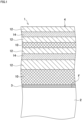
- an optical product 1 includes a base member 2 and an optical multilayer film 4 formed above a film formation surface F of the base member 2 via underlayer 3.
- the base member 2 is a base for forming the optical product 1.
- the base member 2 has a plate shape (as in a substrate).
- the shape of the base member 2 may be a flat plate shape, a curved plate shape, or a shape other than a plate shape, such as a block shape.
- the material of the base member 2 As the material of the base member 2, a plastic is used, and a polycarbonate (PC) resin as a thermosetting resin is used herein.
- the material of the base member 2 is not limited to PC and may be, for example, a polyurethane resin, a thiourethane resin, an episulfide resin, a polyester resin, an acrylic resin, a polyethersulfone resin, a poly(4-methylpentene-1) resin, a diethylene glycol bis(allyl carbonate) resin, or a combination of these resins.
- the material of the base member 2 may be one other than plastic, such as glass.
- the film formation surface F of the base member 2 is present at the front surface thereof, and the optical multilayer film 4 is provided above this front surface via the underlayer 3.
- the optical multilayer film 4 may be provided to each of both the front surface and the back surface or may be provided to each of three or more surfaces of a base member 2 having a block shape, or the like. These plurality of optical multilayer films 4 may have configurations identical to one another or may have configurations different from one another with, for example, the film thicknesses of some or all of the optical multilayer films being different.
- the optical multilayer film 4 may be provided directly on the film formation surface F of the base member 2 without providing any underlayer 3.
- the underlayer 3 may be composed of a plurality of layers.
- a front layer film such as an antifouling film (a water-repellent film, an oil-repellent film, or a water-repellent and oil-repellent film) may be provided on the front surface side (an air side, i.e., an opposite side to the base member 2) of the optical multilayer film 4.
- an antifouling film a water-repellent film, an oil-repellent film, or a water-repellent and oil-repellent film
- the underlayer 3 is provided to attain at least one of the following two objects. That is, firstly, the underlayer 3 is provided to cause the adhesiveness of the optical multilayer film 4 (in particular, an Al layer 10 as a first layer counted from the base member 2 side (the same applies below)) to the base member 2 to be higher than that in the case where film formation is performed directly on the base member 2. Secondly, the underlayer 3 is provided to suppress gas emission from the base member 2 and maintain the film quality of the optical multilayer film 4 (the Al layer 10 as the first layer) above the base member 2.
- the underlayer 3 may be provided to attain another object, instead of the at least one of these objects or in addition to the at least one of these objects.
- the underlayer 3 is, for example, alumina (Al 2 O 3 ), chromium (Cr), or a combination of these substances.
- the underlayer 3 may be treated as a constituent (first layer) of the optical multilayer film 4.
- the optical multilayer film 4 is a multilayer film having a structure with a total of eight layers.
- the optical multilayer film 4 includes the Al layer 10 (first Al layer) as the first layer, a low-refractive-index layer 12 (first low-refractive-index layer) as a second layer, a high-refractive-index layer 14 (first high-refractive-index layer) as a third layer, a low-refractive-index layer 12 (second low-refractive-index layer) as a fourth layer, an Al layer 10 (second Al layer) as a fifth layer, a low-refractive-index layer 12 (third low-refractive-index layer) as a sixth layer, a high-refractive-index layer 14 (second high-refractive-index layer) as a seventh layer, and a low-refractive-index layer 12 (fourth low-refractive-index layer) as an eighth layer.
- the optical multilayer film 4 only has to have the structure with these eight layers and may have nine or more layers (for example, ten layers or twelve layers) as a result of further having one or more layers on the base member 2 side relative to the first layer or further having one or more layers on the air side relative to the eighth layer.
- Each of the Al layers 10 is formed of aluminum.
- the Al layer 10 as the first layer reflects or absorbs mainly light having wavelengths in an ultraviolet range to a visible range (for example, light having wavelengths of 300 to 750 nm).
- the visible range is defined as a range from 400 to 750 nm. Therefore, the material of the underlayer 3, and the like, basically do not influence optical properties of the optical multilayer film 4.
- the physical film thickness of the Al layer 10 as the first layer is set to be, for example, not smaller than 100 nm from the viewpoint of ensuring sufficient reflection and absorption.
- the physical film thickness of the Al layer 10 as the first layer is set to be, for example, not larger than 200 nm, not larger than 150 nm, or not larger than 130 nm from the viewpoint of suppressing decrease in reflectance due to increase in surface roughness and suppressing increase in cost due to increase in film thickness.
- the visible range is not limited to the above range and, for example, may have a lower limit of either of 410 and 420 nm or have an upper limit of any of 700, 720, 780, and 800 nm.
- the Al layer 10 as the fifth layer significantly contributes mainly to increase/decrease in the reflectance on a long wavelength side. If the physical film thickness of the Al layer 10 as the fifth layer is zero (the Al layer 10 as the fifth layer is absent), the reflectance on the long wavelength side becomes high relative to the reflectance on a shorter wavelength side than the long wavelength side.
- the physical film thickness of the Al layer 10 as the fifth layer is small, the reflectance on the long wavelength side becomes low relative to the reflectance on the short wavelength side, whereas, if the physical film thickness of the Al layer 10 as the fifth layer is large, the reflectance on the long wavelength side becomes high relative to the reflectance on the short wavelength side.
- Such characteristics are realized mainly through absorption of light on the long wavelength side by the Al layer 10 as the fifth layer.
- the physical film thickness of the Al layer 10 as the fifth layer is mainly adjusted on the basis of such characteristics, the properties, of the optical multilayer film 4, of reflecting light on the short wavelength side and suppressing reflection of light on the longer wavelength side than the light on the short wavelength side are adjusted.
- the optical product 1 (optical multilayer film 4) having such properties can be said to be a long-wavelength absorption type mirror and can be said to be a selective reflection type mirror.
- the Al layer 10 as the fifth layer itself acts as an ordinary mirror formed of a metal and comes to have a high reflectance regardless of whether the reflectance is one on the long wavelength side or the short wavelength side.
- the band on the long wavelength side can be arbitrarily set between the UV range and an infrared range through adjustment in film designing.
- a wavelength range of not shorter than 600 nm may be set as a long wavelength side
- a wavelength range of shorter than 600 nm may be set as a short wavelength side.
- a performance of the optical product 1 that is the lowness regarding reflection of light on the long wavelength side relative to reflection of light on the short wavelength side is expressed with an IR/LTV ratio defined by the following formula (1).
- a lower IR/UV ratio leads to further suppression of reflection of the light on the long wavelength side relative to reflection of the light on the short wavelength side and leads to a more favorable performance of the optical product 1 in which reflection is achieved on the short wavelength side and reflection is suppressed on the long wavelength side as in a cold mirror.
- an optical product in which reflection is achieved on the short wavelength side and reflection is suppressed on the long wavelength side is referred to as a cold mirror regardless of whether the band is on the short wavelength side or the long wavelength side.
- an IR/UV ratio' serving as an index similar to the IR/UV ratio is defined by the following formula (2).
- IR / UV ratio Average reflectance at not shorter than 600 nm and not longer than 800 nm Average reflectance at not shorter than 3 00 nm and not longer than 5 00 nm
- IR / UV ratio ′ Average reflectance at not shorter than 600 nm and not longer than 800 nm Average reflectance at not shorter than 35 0 nm and not longer than 5 00 nm
- the physical film thickness of the Al layer 10 as the fifth layer is set to be, for example, not smaller than 5 nm and not larger than 30 nm from the viewpoint of ensuring more favorable performances (lower IR/UV ratio, IR/UV ratio', and the like) in the optical product 1.
- the physical film thickness of the Al layer 10 as the fifth layer is smaller than 5 nm, it becomes comparatively difficult to uniformly form the Al layer 10 as the fifth layer. Meanwhile, if the physical film thickness of the Al layer 10 as the fifth layer is larger than 30 nm, more of an Al material or the like becomes necessary accordingly, whereby cost increases.
- Each of the low-refractive-index layers 12 is formed of a low-refractive-index material that is an inorganic dielectric and that is a metal oxide or a metal fluoride.
- the low-refractive-index material is, for example, silicon oxide (SiO 2 ), calcium fluoride (CaF 2 ), magnesium fluoride (MgF 2 ), or a mixture of two or more types of these substances.
- Each of the high-refractive-index layers 14 is formed of a high-refractive-index material that is an inorganic dielectric and that is a metal oxide.
- the high-refractive-index material is, for example, tantalum oxide (Ta 2 O 5 ), zirconium oxide (ZrO 2 ), titanium oxide (TiO 2 ), niobium oxide (Nb 2 O 5 ), hafnium oxide (HfO 2 ), selenium oxide (CeO 2 ), aluminum oxide (Al 2 O 3 ), yttrium oxide (YO 2 ), or a mixture of two or more types of these substances.
- At least either of the low-refractive-index layers 12 and the high-refractive-index layers 14 may be formed of materials identical to one another. In this case, film designing is easy, and cost for film formation is low.
- the physical film thickness of each of the low-refractive-index layers 12 and the high-refractive-index layers 14 is mainly a factor in determining a reflection band in the optical multilayer film 4. For example, if the physical film thicknesses of all the low-refractive-index layers 12 and all the high-refractive-index layers 14 are set to be large, the reflection band is shifted to the long wavelength side, whereas, if the physical film thicknesses of all the low-refractive-index layers 12 and all the high-refractive-index layers 14 are set to be small, the reflection band is shifted to the short wavelength side.
- the underlayer 3 and the layers of the optical multilayer film 4 in the optical product 1 are sequentially formed on the film formation surface F of the base member 2 through physical vapor deposition (PVD such as vacuum deposition and sputtering).
- PVD physical vapor deposition
- the underlayer 3 and the layers of the optical multilayer film 4 are produced in the same method from the viewpoint of ensuring ease of production, for example.
- a production method for a part of the underlayer 3 and the layers of the optical multilayer film 4 may be different from a production method for another part.
- FIG. 2 is a schematic diagram of the vapor deposition device 51.
- the vapor deposition device 51 has a chamber 52, a vapor deposition dome 54, a plurality of (here, two) evaporation source holders 56A and 56B, a plurality of (here, two) shutters 57A and 57B, and an ion gun 58.
- the chamber 52 is a sealable container.
- the inside of the chamber 52 is made vacuum by a pump (not shown).
- the vapor deposition dome 54 has a disc shape.
- the vapor deposition dome 54 is horizontally provided so as to be rotatable about a vertical central axis in the chamber 52.
- the vapor deposition dome 54 holds the base member 2.
- the number of the base members 2 to be held by the vapor deposition dome 54 may be one as shown in FIG. 2 or may be two or more.
- the evaporation source holder 56A is disposed so as to be opposed to the vapor deposition dome 54 and retains an evaporation source JA so as to enable heating thereof.
- the evaporation source holder 56B is configured in the same manner as the evaporation source holder 56A, except that the evaporation source holder 56B retains an evaporation source JB so as to enable heating thereof, the evaporation source JB being different from the evaporation source JA.
- the shutter 57A is provided such that the state thereof is switchable between a state of shielding the upper side (vapor deposition dome 54 side) of the evaporation source holder 56A and a state of not shielding said upper side.
- the shutter 57B is provided such that the state thereof is switchable between a state of shielding the upper side of the evaporation source holder 56B and a state of not shielding said upper side.
- the ion gun 58 is provided on the evaporation source holder 56 side and radiates ionized gases (ion beams I) into the chamber 52 (as an ion source).
- the gases are O 2 gas and Ar gas.
- the gases may be replaced with other gases.
- Ar gas may be replaced with another rare gas or may be omitted.
- the evaporation source holder 56A the evaporation source JA, the shutter 57A, and the like, only one set of them may be provided, or three or more sets of them may be provided.
- the inside of the chamber 52 is made vacuum, and the ion gun 58 radiates ionized O 2 gas and ionized Ar gas under respective predetermined conditions as pretreatment so as to clean the base member 2 (ion cleaning). More specifically, even if organic matter or the like is adhered on the base member 2, such radiation of the ion beams I causes the organic matter or the like to be decomposed and peeled off owing to the ion beams I. Through such cleaning, the adhesiveness of each film to be formed later is improved.
- Al 2 O 3 evaporated from the evaporation source JA through the heating turns into the underlayer 3 formed of Al 2 O 3 on the film formation surface F of the base member 2.
- the underlayer 3 is more stably fixed to the film formation surface F of the base member 2 owing to actions of the ion beams I and the like.
- the physical film thickness of the underlayer 3 is controlled according to a vapor deposition rate and a vapor deposition time.
- the physical film thicknesses of the other layers are also controlled in the same manner.
- the evaporation source JA is replaced with a vapor deposition material for each of the low-refractive-index layers 12.
- the vapor deposition material for the low-refractive-index layer 12 is heated and turns into the low-refractive-index layer 12 as the second layer on the Al layer 10.
- operations such as an operation of replacing either of the evaporation sources JA and JB with a vapor deposition material for each of the high-refractive-index layers 14 or the like and an operation of radiating ion beams I based on oxygen gases (including, as appropriate, Ar gas) as necessary, are performed such that the high-refractive-index layer 14 as the third layer, the low-refractive-index layer 12 as the fourth layer, the Al layer 10 as the fifth layer, the low-refractive-index layer 12 as the sixth layer, the high-refractive-index layer 14 as the seventh layer, and the low-refractive-index layer 12 as the eighth layer are sequentially vapor-deposited.
- oxygen gases including, as appropriate, Ar gas
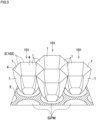
- a plurality of light concentrators 101 are provided correspondingly to a plurality of respective SiPMs.
- Each of the light concentrators 101 is for the CTA.
- Each light concentrator 101 may be used for another purpose.
- the SiPMs are arranged on an element arrangement portion E in a staggered pattern as seen from above.
- the number of the SiPMs provided is, for example, about 2000.
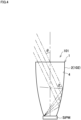
- Each light concentrator 101 has a hexagonal tubular shape. Each light concentrator 101 is disposed on the corresponding SiPM in a state of enclosing a center portion of the SiPM. Each light concentrator 101 dwindles from an upper end portion toward a lower end thereof (in a shape of cone). The coating in the present invention is applied on the inner surface of each light concentrator 101.
- the shape of each light concentrator 101 may be a quadrangular tubular shape or the like, the shape of a part of a tube such as a semi-cylindrical shape, a curved plate shape, or a flat plate shape. Also, each light concentrator 101 may dwindle only at a center portion thereof in the up-down direction or may dwindle from a lower end portion toward an upper end thereof, or does not have to dwindle.
- each light concentrator 101 is, for example, about 70 mm (millimeters).
- the length of one side of a hexagonal opening at the upper end of each light concentrator 101 is, for example, about 50 mm.
- each light concentrator 101 Surfaces (six surfaces) forming each light concentrator 101 are the optical products 1 with the film formation surfaces F being located on the inner surface side.
- the base members 2 in one light concentrator 101 are arranged in a tubular pattern, to form a light concentrator body 102.
- the optical multilayer films 4 are arranged on the inner surface of the light concentrator body 102.
- Each light concentrator 101 is formed of the optical products 1 as cold mirrors.
- each light concentrator 101 may be formed by fixing the optical products 1 including the base members 2 onto the inner surface of a base body having a hexagonal tubular shape. In this case, the base body and the base members 2 form the light concentrator body 102.
- each light concentrator 101 selectively guides a 300-to-500-nm light to the corresponding SiPM by means of the optical multilayer film 4 having a high reflectance for the 300-to-500-nm light and a low reflectance for light in a wavelength range of longer than 500 nm. A part or the entirety of light in the wavelength range of longer than 500 nm is absorbed by the optical multilayer film 4.
- Infrared rays secondarily emitted from the SiPM are light in the wavelength range of longer than 500 nm. Therefore, reflection of the infrared rays on the optical multilayer film 4 is suppressed. Consequently, a situation in which the infrared rays are returned to the SiPM side and influence detection of light on the short wavelength side is inhibited from occurring.
- the light concentrator 101 is arranged in a state where one side of the opening at the upper end of another light concentrator 101 is in contact with one side of the opening at the upper end of an adj acent one of the light concentrator 101.
- a group of light concentrators 101, 101, 101... has a honeycomb shape as seen from above.
- An upper portion of the group of light concentrators 101, 101, 101... forms a honeycomb structure having an external shape with a diameter of, for example, about 3 m (meters).
- the CTA includes the group of light concentrators 101, 101, 101... and the element arrangement portion E, and detects Cherenkov light that comes from the night sky and that is concentrated within 300 to 500 nm.
- An optical product in embodiment 2 is configured in the same manner as the optical product 1 in embodiment 1, except for the optical multilayer film.
- components configured in the same manner as those of the optical product 1 in embodiment 1 are, as appropriate, denoted by the same reference characters and not described.
- the configuration of an optical multilayer film in embodiment 2 differs from that of the optical multilayer film 4 in embodiment 1, but, similar to the optical multilayer film 4 in embodiment 1, satisfies the following various conditions.
- the optical multilayer film in embodiment 2 includes a low-refractive-index layer 12 formed of a dielectric, a high-refractive-index layer 14 formed of a dielectric, a metal layer formed of a metal, and a second Al layer formed of Al.
- the metal layer is, for example, a first Al layer formed of Al or an Ag layer formed of Ag (silver).
- the physical film thickness of the metal layer is preferably not smaller than 20 nm.
- a third Al layer formed of Al may further be disposed, and, likewise, fourth and subsequent Al layers formed of Al may be disposed as appropriate.
- the metal layer is disposed between the second Al layer and the base member 2 and preferably disposed as a first layer counted from the base member 2 side. If the metal layer is an Ag layer or the like (formed of a material other than Al), no first Al layer is present. However, in order to maintain clarity, the second Al layer is not renamed, i.e., remains the second Al layer, and, if a third Al layer is further present, third and subsequent Al layers are not renamed, either.
- At least either of one or more low-refractive-index layers 12 and one or more high-refractive-index layers 14 are disposed between the metal layer and the second Al layer.
- At least either of one or more low-refractive-index layers 12 and one or more high-refractive-index layers 14 are disposed on the air side relative to the second Al layer.
- Each of the layers of the optical multilayer film in embodiment 2 is formed in the same manner as the corresponding layer of the optical multilayer film 4 in embodiment 1.
- the Al layer that is closest to the air side significantly contributes mainly to increase/decrease in the reflectance on the long wavelength side in the same manner as the Al layer 10 as the fifth layer (closest to the air side) in embodiment 1. If the physical film thickness of the Al layer 10 as the fifth layer is zero (i.e., the Al layer 10 as the fifth layer is absent), the reflectance on the long wavelength side becomes high relative to the reflectance on the shorter wavelength side than the long wavelength side.
- the physical film thickness of the Al layer that is closest to the air side is small, the reflectance on the long wavelength side becomes low relative to the reflectance on the short wavelength side, whereas, if the physical film thickness of the Al layer that is closest to the air side is large, the reflectance on the long wavelength side becomes high relative to the reflectance on the short wavelength side.
- Such characteristics are realized mainly through absorption of light on the long wavelength side by the Al layer that is closest to the air side.
- the physical film thickness of the Al layer that is closest to the air side is mainly adjusted on the basis of such characteristics, the properties, of the optical multilayer film 4, of reflecting light on the short wavelength side and suppressing reflection of light on the longer wavelength side than the light on the short wavelength side are adjusted.
- the Al layer that is closest to the air side itself acts as an ordinary mirror formed of a metal and comes to have a high reflectance regardless of whether the reflectance is one on the long wavelength side or the short wavelength side.
- Each of bands on the long wavelength side and the short wavelength side in embodiment 2 can be arbitrarily set between the UV range and the infrared range through adjustment in film designing in the same manner as that in embodiment 1.
- the short wavelength side is set to be 300 to 500 nm
- the long wavelength side is set to be 600 to 800 nm
- a performance can be evaluated according to various IR/LTV ratios.
- the short wavelength side can be set to be 400 to 600 nm
- the long wavelength side can be set to be 700 to 900 nm.
- a performance that is the lowness regarding reflection of light on the long wavelength side relative to reflection of light on the short wavelength side is expressed with an IR/VL ratio that is similar to the IR/UV ratio and that is defined by the following formula (3).
- the short wavelength side may be set to be 400 to 600 nm
- the long wavelength side may be set to be 700 to 900 nm
- the performance may be evaluated according to the IR/VL ratio.
- at least either of the upper limit and the lower limit of the wavelength range on the short wavelength side and the upper limit and the lower limit of the wavelength range on the long wavelength side may be changed.
- the periscope camera is a camera in which visible light (VL) from a lens is turned back by a mirror as in a periscope so as to be sent to an imaging element disposed at an angle (for example, 90°) different from that of the lens so that imaging is performed.
- VL visible light
- the periscope camera is compact for the length of the optical path, and thus is built in, for example, a mobile terminal.
- the imaging element is sensitive also to near-infrared rays (IR) in addition to visible light. Near-infrared rays that can hardly be seen could adversely influence an image that is generated.
- IR / VL ratio Average reflectance at not shorter than 7 00 nm and not longer than 9 00 nm Average reflectance at not shorter than 4 00 nm and not longer than 6 00 nm
- the physical film thickness of the second Al layer that is closest to the air side is preferably not smaller than 5 nm and not larger than 35 nm and more preferably not smaller than 5 nm and not larger than 30 nm from the viewpoint of ensuring more favorable performances (lower IR/UV ratio, IR/UV ratio', IR/VL ratio, and the like) in the optical product, for example.
- the physical film thickness of the Al layer that is closest to the air side is preferably set to be not smaller than 5 nm and not larger than 35 nm and more preferably set to be not smaller than 5 nm and not larger than 30 nm in the same manner.
- the physical film thickness of the Al layer that is closest to the air side is smaller than 5 nm, it becomes comparatively difficult to uniformly form the Al layer that is closest to the air side. Meanwhile, if the physical film thickness of the Al layer that is closest to the air side is larger than 35 nm, more of an Al material or the like becomes necessary accordingly, whereby cost increases.
- An optical multilayer film in embodiment 2-1 belonging to such embodiment 2 has a total of six layers which are a first Al layer (metal layer), a low-refractive-index layer 12, a high-refractive-index layer 14, a second Al layer, a low-refractive-index layer 12, and a high-refractive-index layer 14 in order from the first layer.
- the physical film thickness of the first Al layer as the first layer is not smaller than 20 nm.
- the physical film thickness of the second Al layer as the fourth layer is not smaller than 5 nm and not larger than 30 nm.
- the metal layer is defined as "M”
- the Al layer is defined as “A”
- each of the low-refractive-index layers 12 is defined as “L”
- each of the high-refractive-index layers 14 is defined as "H”
- the optical multilayer film in embodiment 2-1 is expressed as "MLHALH”.
- an optical multilayer film in embodiment 2-2 belonging to embodiment 2 has a total of six layers which are a first Al layer (metal layer), a low-refractive-index layer 12, a high-refractive-index layer 14, a second Al layer, a low-refractive-index layer 12, and a high-refractive-index layer 14 in order from the first layer.
- the physical film thickness of the first Al layer as the first layer is not smaller than 20 nm.
- the physical film thickness of the second Al layer as the fourth layer is not smaller than 5 nm and not larger than 30 nm.
- the optical multilayer film in embodiment 2-2 is expressed as "MLHALH" in the same manner as that in embodiment 2-1.
- an optical multilayer film in embodiment 2-3 belonging to embodiment 2 has a total of six layers which are an Ag layer (metal layer), a low-refractive-index layer 12, a high-refractive-index layer 14, a second Al layer, a low-refractive-index layer 12, and a high-refractive-index layer 14 in order from the first layer.
- the physical film thickness of the Ag layer as the first layer is not smaller than 20 nm.
- the physical film thickness of the second Al layer as the fourth layer is not smaller than 5 nm and not larger than 30 nm.
- the optical multilayer film in embodiment 2-3 is expressed as "MLHALH" in the same manner as that in embodiment 2-1.
- an optical multilayer film in embodiment 2-4 belonging to embodiment 2 has a total of five layers which are a first Al layer (metal layer), a low-refractive-index layer 12, a high-refractive-index layer 14, a second Al layer, and a high-refractive-index layer 14 in order from the first layer.
- the physical film thickness of the first Al layer as the first layer is not smaller than 20 nm.
- the physical film thickness of the second Al layer as the fourth layer is not smaller than 5 nm and not larger than 30 nm.
- the optical multilayer film in embodiment 2-4 is expressed as "MLHAH".
- an optical multilayer film in embodiment 2-5 belonging to embodiment 2 has a total of nine layers which are a first Al layer (metal layer), a low-refractive-index layer 12, a high-refractive-index layer 14, a second Al layer, a low-refractive-index layer 12, a high-refractive-index layer 14, a third Al layer, a low-refractive-index layer 12, and a high-refractive-index layer 14 in order from the first layer.
- the physical film thickness of the first Al layer as the first layer is not smaller than 20 nm.
- the physical film thickness of the third Al layer as the seventh layer is not smaller than 5 nm and not larger than 30 nm.
- the optical multilayer film in embodiment 2-5 is expressed as "MLHALHALH". If the number of times "LHA" is repeated is written on the upper right of "LHA", the optical multilayer film in embodiment 2-5 is expressed as "M(LHA) 2 LH".
- an optical multilayer film in embodiment 2-6 belonging to embodiment 2 has a total of eleven layers which are a first Al layer (metal layer), a low-refractive-index layer 12, a high-refractive-index layer 14, a low-refractive-index layer 12, a high-refractive-index layer 14, a second Al layer, a low-refractive-index layer 12, a high-refractive-index layer 14, a third Al layer, a low-refractive-index layer 12, and a high-refractive-index layer 14 in order from the first layer.
- the physical film thickness of the first Al layer as the first layer is not smaller than 20 nm.
- the physical film thickness of the third Al layer as the ninth layer is not smaller than 5 nm and not larger than 30 nm.
- the optical multilayer film in embodiment 2-6 is expressed as "MLHLHALHALH" or "MLH(LHA) 2 LH".
- an optical multilayer film in embodiment 2-7 belonging to embodiment 2 has a total of eleven layers which are a first Al layer (metal layer), a high-refractive-index layer 14, a second Al layer, a low-refractive-index layer 12, a high-refractive-index layer 14, a third Al layer, a low-refractive-index layer 12, a high-refractive-index layer 14, a fourth Al layer, a low-refractive-index layer 12, and a high-refractive-index layer 14 in order from the first layer.
- the physical film thickness of the first Al layer as the first layer is not smaller than 20 nm.
- the physical film thickness of the fourth Al layer as the ninth layer is not smaller than 5 nm and not larger than 30 nm.
- the optical multilayer film in embodiment 2-7 is expressed as "MHALHALHALH" or "MHA(LHA) 2 LH".
- An optical product in embodiment 3 is configured in the same manner as the optical product in embodiment 2.
- An optical multilayer film in embodiment 3-1 belonging to embodiment 3 has a total of four layers and has a configuration of "MHAL".
- An optical multilayer film in embodiment 3-2 belonging to embodiment 3 has a total of four layers and has a configuration of "MLAL".
- An optical multilayer film in embodiment 3-3 belonging to embodiment 3 has a total of five layers and has a configuration of "MLHAH".
- An optical multilayer film in embodiment 3-4 belonging to embodiment 3 has a total of eight layers and has a configuration of "MLHALHAH".
- the optical multilayer film in embodiment 3-4 is obtained by repeating one set of "LHA" of the optical multilayer film in embodiment 3-3 so as to have two such sets adjacent to each other, i.e., so as to be configured as "M(LHA) 2 H".
- An optical multilayer film in embodiment 3-5 belonging to embodiment 3 has a total of eleven layers and has a configuration of "MLHALHALHAH".
- the optical multilayer film in embodiment 3-5 is obtained by repeating one set of "LHA" of the optical multilayer film in embodiment 3-3 so as to have three such sets that are consecutive, i.e., so as to be configured as "M(LHA) 3 H".
- An optical multilayer film in embodiment 3-6 belonging to embodiment 3 has a total of fourteen layers and has a configuration of "MLHALHALHALHAH".
- the optical multilayer film in embodiment 3-6 is obtained by repeating one set of "LHA" of the optical multilayer film in embodiment 3-3 so as to have four such sets that are consecutive, i.e., so as to be configured as "M(LHA) 4 H".
- An optical multilayer film in embodiment 3-7 belonging to embodiment 3 has a total of seventeen layers and has a configuration of "MLHALHALHALHALHAH".
- the optical multilayer film in embodiment 3-7 is obtained by repeating one set of "LHA" of the optical multilayer film in embodiment 3-3 so as to have five such sets that are consecutive, i.e., so as to be configured as "M(LHA) 5 H".
- An optical multilayer film in embodiment 3-8 belonging to embodiment 3 has a total of eight layers and has a configuration of "MLHLALHL".
- Embodiment 3-8 is the same as embodiment 1.
- the present invention is not limited to the following examples. According to interpretation of the present invention, the following examples may be substantially regarded as comparative examples, or the following comparative examples may be substantially regarded as examples.
- an optical multilayer film having a favorable IR/UV ratio was designed as follows.
- Ta 2 O 5 was selected as a high-refractive-index material
- SiO 2 was selected as a low-refractive-index material
- an optical multilayer film including a total of 66 layers and having a total physical film thickness of 4275.4 nm was designed.
- optical constants shown in FIG. 5 , FIG. 6 , and FIG. 7 were used in this order.
- the extinction coefficient of SiO 2 is zero over the entire wavelength range (horizontal axis) in FIG. 7 .
- the ordinal number (counted from the base member 2 side), the material, and the physical film thickness (nm) of each of the layers are indicated in the following Table 1.
- comparative example 1 was actually produced on a base member by the vapor deposition device 51 on the basis of the design of comparative example 1.
- the base member was a substrate formed of PC and having a shape obtained by vertically dividing the light concentrator 101 into three pieces (opening pieces at 120°).
- Vapor deposition conditions for comparative example 1 were set as indicated in two upper rows of the following Table 2.
- conditions of ion assist were set as indicated in the corresponding rows of the following Table 3.
- comparative example 1 PC substrate
- the temperature of the substrate was raised to 120°C, and a thermal stress was applied to the substrate, to cause deformation.
- the total physical film thickness of the optical multilayer film was 4275.4 nm and was comparatively large, and occurrence of a film stress led to generation of a crack in the optical multilayer film.
- An IR/UV ratio calculated on the basis of FIG. 9 was 0.202 (20.2%) which was higher than a simulative value.
- a substrate was formed of, instead of PC, glass (D263Teco manufactured by SCHOTT Japan Corporation) having a thickness of 0.1 mm and having a square shape with one side being 76 mm, and comparative example 1 (glass substrate) was actually produced in the same manner as that in the case of the substrate formed of PC.
- glass D263Teco manufactured by SCHOTT Japan Corporation
- comparative example 1 glass substrate
- comparative example 1 glass substrate
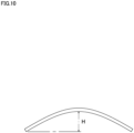
- the maximum height difference H in height was 2 mm.
- the above incident angle ⁇ and the collection efficiency (%) for each of light having various wavelengths were simulated.
- the light concentrator is configured in the same manner as the above light concentrator 101, except for the type of the optical multilayer film on the inner surface.
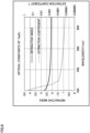
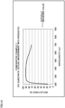
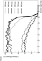
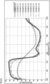
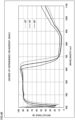
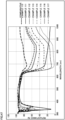
- FIG. 11 is a graph indicating the relationship between wavelength (280 to 820 nm) and various types of photon detection efficiencies (PDE: %).
- SiPM (75- ⁇ m cell size) which is the uppermost curve at 500 nm indicates an SiPM in which the cell size of an element is 75 ⁇ m
- SiPM (50- ⁇ m cell size) which is the second curve from the uppermost one at 500 nm indicates an SiPM in which the cell size of an element is 50 ⁇ m
- PMT QE x 90% Col.
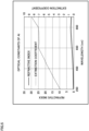
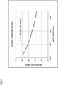
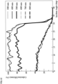
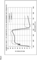
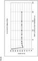
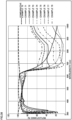
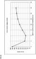
- FIG. 12 is a graph related to the relationship between the incident angle ⁇ (horizontal axis) of, and the collection efficiency (vertical axis) for, each of light that had the various wavelengths and that were incident on the light concentrator in comparative example 1.
- the collection efficiency at 300 to 500 nm is higher than 70%, whereas the collection efficiency is decreased to be not higher than 40% at not shorter than 600 nm.
- this light concentrator is suitable for SiPMs.
- the following optical multilayer film was designed on the basis of an optical multilayer film (high-reflection mirror) applied on the inner surface of a conventional light concentrator for the CTA, for which PMTs were used.
- comparative example 2 in which an Al layer as a first layer, an SiO 2 layer formed of SiO 2 as a second layer, and a TazOs layer formed of Ta 2 O 5 as a third layer were stacked on an adhesion layer formed of Al 2 O 3 was designed as in the following Table 4. [Table 4] Ordinal number of layer, etc. Material of film Film thickness (nm) Adhesion layer Al 2 O 3 10.0 First layer Al 120.0 Second layer SiO 2 72.6 Third layer Ta 2 O 5 20.1 Total film thickness 222.7
- the reflectance in comparative example 2 is high at both 300 to 500 nm and 600 to 800 nm to similar extents, and the IR/UV ratio in comparative example 2 is 0.81 (81%) and is comparatively high.
- comparative example 2 can hardly be said to be a cold mirror and is difficult to use for SiPMs.
- comparative example 2 was actually produced on a base member by the vapor deposition device 51 on the basis of the design of comparative example 2.
- the base member the same substrate as that for comparative example 1 (PC substrate) was used.
- This spectral reflectance distribution does not significantly differ from the simulative spectral reflectance distribution of comparative example 2.
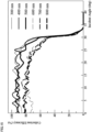
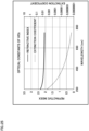
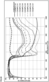
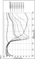
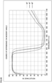
- FIG. 15 is a graph related to the relationship between the incident angle ⁇ (horizontal axis) of, and the collection efficiency (vertical axis) for, each of light that had the various wavelengths and that were incident on the light concentrator in comparative example 2.
- the collection efficiency is higher than about 70% not only at 300 to 500 nm but also at not shorter than 600 nm. In this respect, this light concentrator is not suitable for SiPMs.
- optical products 1 based on the above embodiment were designed and subjected to simulation.
- Physical film thicknesses other than the physical film thickness of the Al layer 10 as the fifth layer in the optical multilayer film 4 are equal among examples 1 to 9. Also, the physical film thickness of the underlayer 3 is equal thereamong.
- comparative example 3 in which the physical film thickness of the Al layer 10 as the fifth layer in the optical multilayer film 4 was set to zero (i.e., the Al layer 10 was not provided) and the physical film thicknesses of the other layers were the same as those in examples 1 to 9, was also designed and subjected to simulation.
- the IR/UV ratio is almost 90%. Meanwhile, in each of examples 1 to 9 in which the Al layer 10 as the fifth layer is present, the IR/UV ratio is not higher than 75%.
- the IR/UV ratio is not higher than 70%.
- example 3-1 an article in which the physical film thicknesses of all the low-refractive-index layers 12 formed of SiO 2 were set to be 0.95 times those in example 3 and the physical film thicknesses of all the high-refractive-index layers 14 formed of Ta 2 O 5 were set to be 0.95 times those in example 3, was designed and subjected to simulation.
- example 3-2 an article in which the physical film thicknesses of all the low-refractive-index layers 12 formed of SiO 2 were set to be 1.05 times those in example 3 and the physical film thicknesses of all the high-refractive-index layers 14 formed of Ta 2 O 5 were set to be 1.05 times those in example 3, was designed and subjected to simulation.
- optical multilayer films 4 in examples 2 to 5 were actually produced on base members by the vapor deposition device 51 on the basis of designs of examples 2 to 5.
- the same substrate as that for comparative example 1 PC substrate
- test pieces in which the optical multilayer films 4 in examples 2 to 5 were vapor-deposited on respective substrates formed of white glass were produced for spectroscopic measurement.
- each of the optical multilayer films 4 in examples 2 to 5 (PC substrates)
- rise in the temperature of the corresponding substrate was suppressed such that the temperature was not higher than 80°C, whereby the substrate was not deformed.
- stress was suppressed, whereby no crack was generated in the optical multilayer film 4.
- examples 2 to 5 white glass substrates
- PC substrates Various conditions for examples 2 to 5 (white glass substrates) were set to the same conditions as those for examples 2 to 5 (PC substrates). Also, the states of the optical multilayer films 4 in examples 2 to 5 (white glass substrates) during and after film formation were the same as those in examples 2 to 5 (PC substrates).
- these spectral reflectance distributions do not significantly differ from simulative spectral reflectance distributions of examples 2 to 5.
- Examples 2 to 5 white glass substrates
- examples 2 to 5 have comparatively low IR/UV ratios and have higher performances.
- thermal stresses, deformation of the substrates, film stresses, and cracks are inhibited from occurring unlike in comparative example 1 (PC substrate).
- examples 2 to 5 white glass substrates
- example 2 (white glass substrate) in which the physical film thickness of the Al layer 10 as the fifth layer is 10 nm, the reflectance at 300 to 500 nm is lower than a simulative reflectance.
- the Al layer 10 as the fifth layer had a small physical film thickness and in actuality, was a discontinuous film or a non-uniform film.
- the Al layer 10 as the fifth layer having a small physical film thickness as in each of examples 1 and 2 (white glass substrates) and examples 1 and 2 (PC substrates) can be made as a continuous film or uniform film.
- the Al layer 10 as the fifth layer is sandwiched between the low-refractive-index layers 12 formed of SiO 2 and might become a discontinuous film or a non-uniform film depending on the state of the interfaces between the Al layer 10 and the low-refractive-index layers 12.
- example 2-1 (white glass substrate).
- An optical constant of MgF 2 is shown in FIG. 20 .
- the extinction coefficient of MgF 2 is zero over the entire wavelength range (horizontal axis) in FIG. 20 .
- the reflectance in example 2-1 (white glass substrate) is higher than the reflectance in example 2 (white glass substrate) and is approximately equal to the reflectances in examples 3 to 5. Meanwhile, at 600 to 800 nm, the reflectance in example 2-1 (white glass substrate) is slightly higher than the reflectance in example 2 (white glass substrate) but is lower than the reflectances in examples 3 to 5. Therefore, example 2-1 (white glass substrate) has an excellent IR/LTV ratio and is a cold mirror having a higher performance.
- example 3 (glass substrate) was produced in the same manner as that in comparative example 1 (glass substrate).
- example 3 glass substrate
- example 3 can easily be introduced onto a base body by being fixed to the base body, without any significant change in the shape (thickness) of the base body.
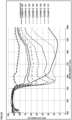
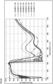
- FIG. 22 to FIG. 24 are graphs related to the relationships between the incident angles ⁇ (horizontal axis) of, and the collection efficiencies (vertical axis) for, each of light that had the various wavelengths and that were incident on the light concentrators 101 in examples 1 to 3, respectively.
- each of the light concentrators 101 in examples 1 to 3 unlike in the light concentrator in comparative example 2, the collection efficiency at 300 to 500 nm is increased to about 60% to 80%, whereas the collection efficiency at not shorter than 600 nm is decreased to about 10% to 40%.
- these light concentrators 101 are suitable for SiPMs. That is, with each of the light concentrators 101 in examples 1 to 3, a signal-to-noise ratio of atmospheric Cerenkov light to night-sky-light is improved.
- each of the light concentrators 101 in examples 1 to 9 can be said to be as follows. That is, in view of production results and the like of examples 2 to 5 (PC substrates) and examples 2 to 5 (white glass substrates), unlike in the light concentrator in comparative example 1, no crack or the like occurs, the lifespan is elongated, and a comparatively high performance can be maintained for a long period.
- examples 11 to 19 and comparative example 13 the materials of all the low-refractive-index layers 12 were MgF 2 , and the materials of all the high-refractive-index layers 14 were HfO 2 .
- the physical film thicknesses of the substrates, the underlayers 3, and the Al layers 10 as the fifth layers, and the like, in examples 11 to 19 and comparative example 13 are equal to those in examples 1 to 9 and comparative example 3, respectively.
- the ordinal numbers, the materials, and the physical film thicknesses (nm) of the respective layers, the total physical film thicknesses, and the IR/UV ratios in examples 11 to 19 and comparative example 13 are indicated in the following Table 7.
- the optical constants of HfO 2 are shown in FIG. 25 .
- the optical constants of Al and MgF 2 are those shown in FIG. 5 and FIG. 20 , respectively.
- the IR/UV ratio is almost 90%. Meanwhile, in each of examples 1 to 9 in which the Al layer 10 as the fifth layer is present, the IR/UV ratio is not higher than 77%.
- the IR/UV ratio is not higher than 72%.
- cold mirrors having higher performances are provided, and a light concentrator 101 formed by using at least any of these cold mirrors guides a 300-to-500-nm light, which is to be observed, to a photodetector and suppresses, mainly through absorption, introduction of a 600-nm-or-longer light, which is not to be observed, to the photodetector.
- examples 21 to 29 and comparative example 23 the materials of all the low-refractive-index layers 12 were SiO 2 , and the materials of all the high-refractive-index layers 14 were HfO 2 .
- the physical film thicknesses of the substrates, the underlayers 3, and the Al layers 10 as the fifth layers, and the like, in examples 21 to 29 and comparative example 23 are equal to those in examples 1 to 9 and comparative example 3, respectively.
- the ordinal numbers, the materials, and the physical film thicknesses (nm) of the respective layers, the total physical film thicknesses, and the IR/UV ratios in examples 21 to 29 and comparative example 23 are indicated in the following Table 8.
- the optical constants of Al, SiO 2 , and HfO 2 are those shown in FIG. 5 , FIG. 7 , and FIG. 25 , respectively.
- the IR/UV ratio is higher than 90%. Meanwhile, in each of examples 21 to 29 in which the Al layer 10 as the fifth layer is present, the IR/UV ratio is not higher than 75%.
- the IR/UV ratio is not higher than 70.1%.
- cold mirrors having higher performances are provided, and a light concentrator 101 formed by using at least any of these cold mirrors guides a 300-to-500-nm light, which is to be observed, to a photodetector and suppresses introduction of a 600-nm-or-longer light, which is not to be observed, to the photodetector.
- examples 31 to 39 and comparative example 33 the materials of all the low-refractive-index layers 12 were SiO 2 , and the materials of all the high-refractive-index layers 14 were TiO 2 .
- the physical film thicknesses of the substrates, the underlayers 3, and the Al layers 10 as the fifth layers, and the like, in examples 31 to 39 and comparative example 33 are equal to those in examples 1 to 9 and comparative example 3, respectively.
- the ordinal numbers, the materials, and the physical film thicknesses (nm) of the respective layers, the total physical film thicknesses, and the IR/UV ratios' in examples 31 to 39 and comparative example 33 are indicated in the following Table 8.
- the optical constants of TiO 2 are shown in FIG. 30 .
- the optical constants of Al and SiO 2 are those shown in FIG. 5 and FIG. 7 , respectively.
- the IR/UV ratio' is 84.5%. Meanwhile, in each of examples 31 to 39 in which the Al layer 10 as the fifth layer is present, the IR/UV ratio' is not higher than 74%.
- the IR/UV ratio' is not higher than 68%.
- cold mirrors having higher performances are provided, and a light concentrator 101 formed by using at least any of these cold mirrors guides a 350-to-500-nm light, which is to be observed, to a photodetector and suppresses introduction of a 600-nm-or-longer light, which is not to be observed, to the photodetector.
- an article for reflecting a visible light mainly light having a wavelength of 400 to 700 nm
- suppressing reflection of near-infrared rays was designed and subjected to simulation.
- FIG. 33 a simulative spectral reflectance distribution regarding light incident in a direction perpendicular to a substrate of example 40 is shown in FIG. 33 .
- Table 10 Substrate Underlayer First layer Second layer Third layer Fourth layer Fifth layer Sixth layer Seventh layer Eighth layer Material PC Al 2 O 3 Al SiO 2 Ta 2 O 5 SiO 2 Al SiO 2 Ta 2 O 5 SiO 2 Film thickness (nm) 10.0 123.0 82.8 51.0 50.3 6.5 47.0 42.9 43.1
- a cold mirror that has a high performance and a long lifespan and that is intended for a band different from those in examples 1 to 39 (short wavelength side: 300 to 500 nm, long wavelength side: 600 to 800 nm), is provided.
- the shape and use regarding the film configuration of the present invention is not limited to the shape and/or use of a Cherenkov light concentrator, and the present invention is applicable to various shapes and uses, as in example 40.
- Each of examples 1 to 40 includes a base member 2 and an optical multilayer film 4 formed indirectly above a film formation surface F of the base member 2.
- the optical multilayer film 4 reflects light on a short wavelength side and suppresses reflection of light on a longer wavelength side than the light on the short wavelength side.
- the optical multilayer film 4 has a first layer, a second layer, a third layer, a fourth layer, a fifth layer, a sixth layer, a seventh layer, and an eighth layer counted from the base member 2 side.
- the first layer is an Al layer 10 as a first layer formed of Al
- the second layer is a low-refractive-index layer 12 as a second layer formed of a low-refractive-index material
- the third layer is a high-refractive-index layer 14 as a third layer formed of a high-refractive-index material
- the fourth layer is a low-refractive-index layer 12 as a fourth layer formed of a low-refractive-index material
- the fifth layer is an Al layer 10 as a fifth layer formed of Al
- the sixth layer is a low-refractive-index layer 12 as a sixth layer formed of a low-refractive-index material
- the seventh layer is a high-refractive-index layer 14 as a seventh layer formed of a high-refractive-index material
- the eighth layer is a low-refractive-index layer 12 as an eighth layer formed of a low-refractive-index material.
- the physical film thickness of the Al layer 10 as the fifth layer is not smaller than 5 nm and not larger than 30 nm. Therefore, an optical product 1 having a more favorable performance is provided.
- each of examples 1 to 39 light on the short wavelength side on which a higher reflectance is obtained than on the long wavelength side is light in a wavelength range of shorter than 600 nm (not shorter than 300 nm and not longer than 500 nm). Therefore, these examples are more suitable for light concentrators 101 intended for a gamma ray observation apparatus such as the CTA.
- example 40 light on the short wavelength side on which a higher reflectance is obtained than on the long wavelength side is light in a wavelength range of not shorter than 400 nm and not longer than 700 nm. Therefore, this example is more suitable for a cold mirror or the like intended for visible light.
- an underlayer 3 for increasing the adhesiveness of the Al layer 10 as the first layer to the base member 2 is provided between the base member 2 and the Al layer 10 as the first layer. Therefore, the optical multilayer film 4 is more stably provided, and the performance of the optical product 1 is more stably exhibited.
- each of the low-refractive-index materials is at least any of SiO 2 , CaF 2 , and MgF 2
- each of the high-refractive-index materials is at least any of Ta 2 O 5 , ZrO 2 , TiO 2 , Nb 2 O 5 , HfO 2 , CeO 2 , Al 2 O 3 , and YO 2 , whereby the optical product 1 is more easily formed.
- a light concentrator 101 capable of increasing the sensitivity of detecting light in a predetermined wavelength range such as Cherenkov light is provided.
- the light concentrator 101 includes a light concentrator body 102 having a tubular shape or a shape that is a part of the tubular shape, and the optical multilayer films 4 in any of examples 1 to 40 are disposed on the inner surface of the light concentrator body 102, it becomes possible to more easily provide a light concentrator 101 capable of increasing the sensitivity of detecting light in the predetermined wavelength range.
- the light concentrator 101 in which the optical multilayer films 4 in any of examples 1 to 39 are disposed is for a gamma ray observation apparatus, and thus a light concentrator 101, for a gamma ray observation apparatus, that has a more excellent performance is provided.
- optical products based on the above embodiment 2-1 were designed for reflection of UV and transmission of IR (for a light concentrator or the like) and were subjected to simulation. Numbers for examples 41 to 50 and comparative examples 34 to 52 have been skipped.
- Physical film thicknesses other than the physical film thickness of the metal layer (first Al layer) as the first layer in the optical multilayer film (MLHALH) in embodiment 2-1 are equal among examples 51 to 56. Also, the physical film thickness of the underlayer 3 is equal (10 nm) thereamong.
- the IR/UV ratios in examples with first layers having physical film thicknesses of 130, 150, and 200 nm are also shown.
- the IR/UV ratio is not lower than 40%. Meanwhile, in each of examples 51 to 56 in which the physical film thickness of the first Al layer as the first layer is not smaller than 20 nm and comparative example 54 in which the physical film thickness of the first Al layer as the first layer is 10 nm, the IR/UV ratio is not higher than 25%.
- the physical film thickness of the first Al layer is preferably not smaller than 20 nm.
- optical products based on the above embodiment 2-2 were designed for reflection of UV and transmission of IR (for a light concentrator or the like) and were subjected to simulation. Numbers for examples 57 to 60 and comparative examples 55 to 62 have been skipped.
- Physical film thicknesses other than the physical film thickness of the second Al layer as the fourth layer in the optical multilayer film (MLHALH) in embodiment 2-2 are equal among examples 61 to 67. Also, the physical film thickness of the underlayer 3 is equal (10 nm) thereamong.
- comparative example 63 in which the physical film thickness of the second Al layer as the fourth layer in the optical multilayer film was set to 0 nm and the physical film thicknesses of the other layers were set to be equal to those in examples 61 to 67, was also designed and subjected to simulation.
- the IR/UV ratio is not lower than 90%.
- the IR/UV ratio is not higher than 70%.
- the IR/UV ratio is not higher than 65%.
- the physical film thickness of the second Al layer is preferably not smaller than 5 nm and not larger than 35 nm and more preferably not smaller than 5 nm and not larger than 30 nm.
- Embodiment 2-3 is obtained by changing the first layer (metal layer) of the optical multilayer film in embodiment 2-2 from the first Al layer to the Ag layer. Numbers for examples 68 to 70 and comparative examples 64 to 72 have been skipped.
- Physical film thicknesses other than the physical film thickness of the second Al layer as the fourth layer in the optical multilayer film (MLHALH) in embodiment 2-3 are equal among examples 71 to 78. Also, the physical film thickness of the underlayer 3 is equal (10 nm) thereamong.
- comparative example 73 in which the physical film thickness of the second Al layer as the fourth layer in the optical multilayer film was set to 0 nm and the physical film thicknesses of the other layers were set to be equal to those in examples 71 to 78, was also designed and subjected to simulation.
- the IR/VL ratios in examples with fourth layers having physical film thicknesses of 40, 50, and 60 nm are also shown.
- the IR/VL ratio is higher than 100%.
- the IR/VL ratio is not higher than 60%.
- the IR/VL ratio is not higher than 55%.
- the physical film thickness of the second Al layer is preferably not smaller than 5 nm and not larger than 35 nm and more preferably not smaller than 5 nm and not larger than 30 nm.
- an imaging element has a spread, and thus it is preferable that the basic reflection angle ⁇ is set to, for example, 45°, and spectral reflection (transmission) performances on the short wavelength side and the long wavelength side are stable also over a certain range of reflection angles ⁇ (for example, 45° ⁇ 15°).
- ⁇ for example, 45° ⁇ 15°
- optical products based on the above embodiment 2-4 were designed for reflection of UV and transmission of IR (for a light concentrator or the like) and were subjected to simulation. Numbers for examples 79 and 80 and comparative examples 74 to 82 have been skipped.
- Physical film thicknesses other than the physical film thickness of the second Al layer as the fourth layer in the optical multilayer film (MLHAH) in embodiment 2-4 are equal among examples 81 to 87. Also, the physical film thickness of the underlayer 3 is equal (10 nm) thereamong.
- comparative example 83 in which the physical film thickness of the second Al layer as the fourth layer in the optical multilayer film was set to 0 nm and the physical film thicknesses of the other layers were set to be equal to those in examples 81 to 87, was also designed and subjected to simulation.
- the IR/UV ratio is not lower than 95%.
- the IR/UV ratio is not higher than 75%.
- the IR/UV ratio is not higher than 70.2%.
- the physical film thickness of the second Al layer is preferably not smaller than 5 nm and not larger than 35 nm and more preferably not smaller than 5 nm and not larger than 30 nm.
- optical products based on the above embodiment 2-5 were designed for reflection of UV and transmission of IR (for a light concentrator or the like) and were subjected to simulation. Numbers for examples 88 to 90 and comparative examples 84 to 92 have been skipped.
- Physical film thicknesses other than the physical film thickness of the third Al layer as the seventh layer in the optical multilayer film (MLHALHALH) in embodiment 2-5 are equal among examples 91 to 97. Also, the physical film thickness of the underlayer 3 is equal (10 nm) thereamong.
- comparative example 93 in which the physical film thickness of the third Al layer as the seventh layer in the optical multilayer film was set to 0 nm and the physical film thicknesses of the other layers were set to be equal to those in examples 91 to 97, was also designed and subjected to simulation.
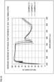
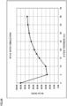
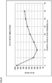
- FIG. 44 the relationship between the IR/UV ratio (%) and the physical film thickness of the third Al layer as the seventh layer (seventh-layer Al film thickness: nm) in a simulation in each of examples 91 to 97 and comparative example 93, is shown in FIG. 44 .
- the IR/UV ratio is not lower than 90%.
- the IR/UV ratio is not higher than 72%.
- the IR/UV ratio is not higher than 70%.
- the physical film thickness of the third Al layer is preferably not smaller than 5 nm and not larger than 35 nm and more preferably not smaller than 5 nm and not larger than 30 nm.
- optical products based on the above embodiment 2-6 were designed for reflection of UV and transmission of IR (for a light concentrator or the like) and were subjected to simulation. Numbers for examples 98 to 100 and comparative examples 94 to 102 have been skipped.
- Physical film thicknesses other than the physical film thickness of the third Al layer as the ninth layer in the optical multilayer film (MLHLHALHALH) in embodiment 2-6 are equal among examples 101 to 107. Also, the physical film thickness of the underlayer 3 is equal (10 nm) thereamong.
- comparative example 103 in which the physical film thickness of the third Al layer as the ninth layer in the optical multilayer film was set to 0 nm and the physical film thicknesses of the other layers were set to be equal to those in examples 101 to 107, was also designed and subjected to simulation.
- FIG. 46 the relationship between the IR/UV ratio (%) and the physical film thickness of the third Al layer as the ninth layer (ninth-layer Al film thickness: nm) in a simulation in each of examples 101 to 107 and comparative example 103, is shown in FIG. 46 .
- [Table 16] M L H L H A L H A L H First layer Second layer Third layer Fourth layer Fifth layer Sixth layer Seventh layer Eighth layer Ninth layer
- Tenth layer Eleventh layer IR/UV ratio Al SiO 2 HfO 2 SiO 2 HfO 2 Al SiO 2 HfO 2 Al SiO 2 HfO 2 Al SiO 2 HfO 2 Com. 103 130.0 53.8 33.0 13.0 60.3 34.5 62.7 72.9 0.0 31.5 45.0 91.4% Ex.
- the IR/UV ratio is not lower than 90%.
- the IR/UV ratio is not higher than 72%.
- the IR/UV ratio is not higher than 70%.
- the physical film thickness of the third Al layer is preferably not smaller than 5 nm and not larger than 35 nm and more preferably not smaller than 5 nm and not larger than 30 nm.
- optical products based on the above embodiment 2-7 were designed for reflection of VL and transmission of IR (for a periscope camera or the like) and were subjected to simulation. Numbers for examples 108 to 110 and comparative examples 104 to 112 have been skipped.
- Physical film thicknesses other than the physical film thickness of the fourth Al layer as the ninth layer in the optical multilayer film (MHALHALHALH) in embodiment 2-7 are equal among examples 111 to 117. Also, the physical film thickness of the underlayer 3 is equal (10 nm) thereamong.
- comparative example 113 in which the physical film thickness of the fourth Al layer as the ninth layer in the optical multilayer film was set to 0 nm and the physical film thicknesses of the other layers were set to be equal to those in examples 111 to 117, was also designed and subjected to simulation.
- FIG. 48 the relationship between the IR/VL ratio (%) and the physical film thickness of the fourth Al layer as the ninth layer (ninth-layer Al film thickness: nm) in a simulation in each of examples 111 to 117 and comparative example 113, is shown in FIG. 48 .
- the IR/VL ratio in an example in which the physical film thickness of the ninth layer is 9 nm is also shown.
- the IR/VL ratio is higher than 85%.
- the IR/VL ratio is not higher than 63%.
- the IR/VL ratio is not higher than 60%.
- the physical film thickness of the fourth Al layer is preferably not smaller than 5 nm and not larger than 35 nm and more preferably not smaller than 5 nm and not larger than 30 nm.
- optical products respectively based on the above embodiments 3-1 to 3-8 were designed for reflection of UV and transmission of IR (for a light concentrator or the like) and were subjected to simulation. Numbers for examples 118 to 120 have been skipped.
- the physical film thickness of the Al layer that is closest to the air side is 10 nm.
- the physical film thickness of the Al layer that is closest to the air side is 5 nm.
- the physical film thickness of the underlayer 3 is equal (10 nm) among examples 121 to 128.
- Example 121 Example 122 Example 123 Example 124 Example 125 Example 126 Example 127 Example 128 Material Film thickness Material Film thickness Material Film thickness Material Film thickness Material Film thickness Material Film thickness Material Film thickness Underlayer Al 2 O 3 10.0 Al 2 O 3 10.0 Al 2 O 3 10.0 Al 2 O 3 10.0 Al 2 O 3 10.0 Al 2 O 3 10.0 Al 2 O 3 10.0 Al 2 O 3 10.0 Al 2 O 3 10.0 Al 2 O 3 10.0 Al 2 O 3 10.0 Al 2 O 3 10.0 First layer Al 130.0 Al 130.0 Al 130.0 Al 130.0 Al 130.0 Al 130.0 Al 130.0 Al 130.0 Al 130.0 Al 130.0 Al 130.0 Al 123.0 Second layer HfO 2 121.2 SiO 2 209.5 SiO 2 94.5 SiO 2 94.5 SiO 2 94.5 SiO 2 94.5 SiO 2 94.5 SiO 2 94.5 SiO 2 69.0 Third layer Al 10.0 Al 10.0 HfO 2 65.8 HfO 2 65.8 HfO 2 65.8 HfO 2 65.8 HfO 2 65.8 Hf
- Each of examples 51 to 128 includes a base member 2 and an optical multilayer film formed indirectly above a film formation surface F of the base member 2.
- the optical multilayer film reflects light on a short wavelength side and suppresses reflection of light on a longer wavelength side than the light on the short wavelength side.
- the optical multilayer film has a first layer counted from the base member 2 side, the first layer being a metal layer M formed of a metal.
- the optical multilayer film further has one or more Al layers A, at least one of a low-refractive-index layer L disposed on the base member 2 side relative to each of the Al layers A and formed of a low-refractive-index material and a high-refractive-index layer H disposed on the base member 2 side relative to the Al layer A and formed of a high-refractive-index material, and at least one of a low-refractive-index layer L disposed on an air side relative to the Al layer A and formed of a low-refractive-index material and a high-refractive-index layer H disposed on the air side relative to the Al layer A and formed of a high-refractive-index material.
- the metal layer M has a physical film thickness of not smaller than 20 nm.
- the Al layer A that is closest to the air side has a physical film thickness of not smaller than 5 nm and not larger than 35 nm.
- the high-refractive-index layer H is disposed to be adjacent to the substrate 2 side of the Al layer A that is closest to the air side
- the low-refractive-index layer L is disposed to be adjacent to the air side of the Al layer A that is closest to the air side. That is, "HAL" is attained for the Al layer A that is closest to the air side. Therefore, an optical product having a more favorable performance is provided.
- the underlayer 3 for increasing the adhesiveness of the metal layer M to the base member 2 is provided between the base member 2 and the metal layer M. Therefore, an optical multilayer film is more stably provided, and the performance of the optical product is more stably exhibited.
- the metal is at least one of Al and Ag, and thus an optical product is more easily formed.
- examples 51 to 128 in particular, examples 51 to 67, 81 to 107, and 121 to 128, is used for a light concentrator 101, a light concentrator capable of increasing the sensitivity of detecting light in a predetermined wavelength range such as Cherenkov light is provided.
Landscapes
- Physics & Mathematics (AREA)
- General Physics & Mathematics (AREA)
- Optics & Photonics (AREA)
- Chemical & Material Sciences (AREA)
- Inorganic Chemistry (AREA)
- Health & Medical Sciences (AREA)
- Toxicology (AREA)
- Optical Elements Other Than Lenses (AREA)
Applications Claiming Priority (2)
| Application Number | Priority Date | Filing Date | Title |
|---|---|---|---|
| JP2021031974 | 2021-03-01 | ||
| PCT/JP2022/006466 WO2022185944A1 (fr) | 2021-03-01 | 2022-02-17 | Produit optique et condenseur |
Publications (3)
| Publication Number | Publication Date |
|---|---|
| EP4286902A1 true EP4286902A1 (fr) | 2023-12-06 |
| EP4286902A4 EP4286902A4 (fr) | 2025-01-08 |
| EP4286902B1 EP4286902B1 (fr) | 2026-02-11 |
Family
ID=83154156
Family Applications (1)
| Application Number | Title | Priority Date | Filing Date |
|---|---|---|---|
| EP22763000.1A Active EP4286902B1 (fr) | 2021-03-01 | 2022-02-17 | Produit optique et condenseur |
Country Status (5)
| Country | Link |
|---|---|
| US (1) | US20230408732A1 (fr) |
| EP (1) | EP4286902B1 (fr) |
| JP (1) | JP7751268B2 (fr) |
| CL (1) | CL2023002570A1 (fr) |
| WO (1) | WO2022185944A1 (fr) |
Families Citing this family (1)
| Publication number | Priority date | Publication date | Assignee | Title |
|---|---|---|---|---|
| CN117908175B (zh) * | 2024-03-20 | 2024-07-16 | 四川虹基光玻新材料科技有限公司 | 一种半反射膜及其制备方法和应用 |
Family Cites Families (9)
| Publication number | Priority date | Publication date | Assignee | Title |
|---|---|---|---|---|
| JP3031625B2 (ja) * | 1989-09-20 | 2000-04-10 | 日本真空光学株式会社 | 熱線吸収反射鏡 |
| US5339198A (en) * | 1992-10-16 | 1994-08-16 | The Dow Chemical Company | All-polymeric cold mirror |
| ATE508348T1 (de) * | 2004-03-01 | 2011-05-15 | Applied Materials Gmbh & Co Kg | Verfahren zum aufbringen eines filters auf einer folie |
| JP2006259124A (ja) * | 2005-03-16 | 2006-09-28 | Kawai Optical Co Ltd | コールドミラー |
| KR20080031174A (ko) | 2005-07-29 | 2008-04-08 | 아사히 가라스 가부시키가이샤 | 반사막용 적층체 |
| JP6741586B2 (ja) * | 2014-04-01 | 2020-08-19 | トヨタ モーター エンジニアリング アンド マニュファクチャリング ノース アメリカ,インコーポレイティド | 色シフトのない多層構造 |
| US10816707B2 (en) | 2015-11-27 | 2020-10-27 | Sony Corporation | Gold color tone multilayer coat and reflector including the same |
| WO2019163340A1 (fr) * | 2018-02-22 | 2019-08-29 | 大阪瓦斯株式会社 | Dispositif de refroidissement par rayonnement |
| JP6967193B2 (ja) | 2019-08-26 | 2021-11-17 | Toto株式会社 | トイレ装置およびトイレシステム |
-
2022
- 2022-02-17 EP EP22763000.1A patent/EP4286902B1/fr active Active
- 2022-02-17 JP JP2023503707A patent/JP7751268B2/ja active Active
- 2022-02-17 WO PCT/JP2022/006466 patent/WO2022185944A1/fr not_active Ceased
-
2023
- 2023-08-29 US US18/457,423 patent/US20230408732A1/en active Pending
- 2023-08-30 CL CL2023002570A patent/CL2023002570A1/es unknown
Also Published As
| Publication number | Publication date |
|---|---|
| JP7751268B2 (ja) | 2025-10-08 |
| US20230408732A1 (en) | 2023-12-21 |
| CL2023002570A1 (es) | 2024-02-23 |
| WO2022185944A1 (fr) | 2022-09-09 |
| EP4286902B1 (fr) | 2026-02-11 |
| JPWO2022185944A1 (fr) | 2022-09-09 |
| EP4286902A4 (fr) | 2025-01-08 |
Similar Documents
| Publication | Publication Date | Title |
|---|---|---|
| US7732788B2 (en) | Radiation image converting panel, scintillator panel and radiation image sensor | |
| US6863397B2 (en) | Optical element and eyeglass lens | |
| JP6171401B2 (ja) | シンチレータパネル | |
| US10078142B2 (en) | Sensor integrated metal dielectric filters for solar-blind silicon ultraviolet detectors | |
| US4735488A (en) | Article and coating having improved reflectance suppression | |
| US9557424B2 (en) | Deposition substrate and scintillator panel | |
| US10916356B2 (en) | Reflective optical element | |
| CN105137472B (zh) | 基于表面共振腔结构的定向发射闪烁体器件 | |
| US20230408732A1 (en) | Optical product and light concentrator | |
| Lesser | Antireflection coatings for silicon charge-coupled devices | |
| JP6286369B2 (ja) | Euv波長範囲用ミラー、該ミラーの製造方法、及び該ミラーを具えた投影露光装置 | |
| Serlemitsos et al. | Broad band x-ray astronomical spectroscopy | |
| Soufli et al. | In-band and out-of-band reflectance calibrations of the EUV multilayer mirrors of the Atmospheric Imaging Assembly instrument aboard the Solar Dynamics Observatory | |
| US20230384491A1 (en) | Optical product and optical product manufacturing method | |
| US20170052294A1 (en) | Uv-blocking coating with capping layer for optics | |
| Ota et al. | Plasmonic ultraviolet filter for fast-timing applications | |
| WO2016130582A1 (fr) | Filtres diélectriques en métal intégrés à des capteurs pour détecteurs d'ultraviolets en silicium pour stores solaires | |
| Larruquert et al. | Narrowband mirrors tuned at the desired far UV spectral lines | |
| JPH06148399A (ja) | X線用多層膜ミラーおよびx線顕微鏡 | |
| CN112908807B (zh) | 一种光电阴极及其应用 | |
| JP2018010002A (ja) | シンチレータパネルおよび撮像パネル | |
| JP2004285412A (ja) | 光学機能性フィルムの製造方法及び製造装置 | |
| Gorin et al. | On the increase of ultraviolet radiation detection efficiency in nuclear particle detectors with the help of transparent wavelength shifter films | |
| JP2016172928A (ja) | 蒸着用基板およびシンチレータパネル | |
| Hsiao et al. | Design and fabrication of optical thin films for remote sensing instruments |
Legal Events
| Date | Code | Title | Description |
|---|---|---|---|
| STAA | Information on the status of an ep patent application or granted ep patent |
Free format text: STATUS: THE INTERNATIONAL PUBLICATION HAS BEEN MADE |
|
| PUAI | Public reference made under article 153(3) epc to a published international application that has entered the european phase |
Free format text: ORIGINAL CODE: 0009012 |
|
| STAA | Information on the status of an ep patent application or granted ep patent |
Free format text: STATUS: REQUEST FOR EXAMINATION WAS MADE |
|
| 17P | Request for examination filed |
Effective date: 20230829 |
|
| AK | Designated contracting states |
Kind code of ref document: A1 Designated state(s): AL AT BE BG CH CY CZ DE DK EE ES FI FR GB GR HR HU IE IS IT LI LT LU LV MC MK MT NL NO PL PT RO RS SE SI SK SM TR |
|
| DAV | Request for validation of the european patent (deleted) | ||
| DAX | Request for extension of the european patent (deleted) | ||
| A4 | Supplementary search report drawn up and despatched |
Effective date: 20241210 |
|
| RIC1 | Information provided on ipc code assigned before grant |
Ipc: G02B 5/28 20060101ALI20241205BHEP Ipc: G02B 5/08 20060101ALI20241205BHEP Ipc: G02B 5/26 20060101AFI20241205BHEP |
|
| GRAP | Despatch of communication of intention to grant a patent |
Free format text: ORIGINAL CODE: EPIDOSNIGR1 |
|
| STAA | Information on the status of an ep patent application or granted ep patent |
Free format text: STATUS: GRANT OF PATENT IS INTENDED |
|
| INTG | Intention to grant announced |
Effective date: 20250605 |
|
| GRAJ | Information related to disapproval of communication of intention to grant by the applicant or resumption of examination proceedings by the epo deleted |
Free format text: ORIGINAL CODE: EPIDOSDIGR1 |
|
| STAA | Information on the status of an ep patent application or granted ep patent |
Free format text: STATUS: REQUEST FOR EXAMINATION WAS MADE |
|
| INTC | Intention to grant announced (deleted) | ||
| GRAP | Despatch of communication of intention to grant a patent |
Free format text: ORIGINAL CODE: EPIDOSNIGR1 |
|
| STAA | Information on the status of an ep patent application or granted ep patent |
Free format text: STATUS: GRANT OF PATENT IS INTENDED |
|
| INTG | Intention to grant announced |
Effective date: 20250923 |
|
| GRAS | Grant fee paid |
Free format text: ORIGINAL CODE: EPIDOSNIGR3 |
|
| GRAA | (expected) grant |
Free format text: ORIGINAL CODE: 0009210 |
|
| STAA | Information on the status of an ep patent application or granted ep patent |
Free format text: STATUS: THE PATENT HAS BEEN GRANTED |
|
| AK | Designated contracting states |
Kind code of ref document: B1 Designated state(s): AL AT BE BG CH CY CZ DE DK EE ES FI FR GB GR HR HU IE IS IT LI LT LU LV MC MK MT NL NO PL PT RO RS SE SI SK SM TR |
|
| REG | Reference to a national code |
Ref country code: CH Ref legal event code: F10 Free format text: ST27 STATUS EVENT CODE: U-0-0-F10-F00 (AS PROVIDED BY THE NATIONAL OFFICE) Effective date: 20260211 Ref country code: GB Ref legal event code: FG4D Ref country code: CH Ref legal event code: R17 Free format text: ST27 STATUS EVENT CODE: U-0-0-R10-R17 (AS PROVIDED BY THE NATIONAL OFFICE) Effective date: 20260211 |