EP4283873B1 - Frequenzdetektionsschaltung, arbeitszykluskorrektor und elektronische vorrichtung - Google Patents
Frequenzdetektionsschaltung, arbeitszykluskorrektor und elektronische vorrichtung Download PDFInfo
- Publication number
- EP4283873B1 EP4283873B1 EP22212820.9A EP22212820A EP4283873B1 EP 4283873 B1 EP4283873 B1 EP 4283873B1 EP 22212820 A EP22212820 A EP 22212820A EP 4283873 B1 EP4283873 B1 EP 4283873B1
- Authority
- EP
- European Patent Office
- Prior art keywords
- terminal
- signal
- circuit
- coupled
- capacitor
- Prior art date
- Legal status (The legal status is an assumption and is not a legal conclusion. Google has not performed a legal analysis and makes no representation as to the accuracy of the status listed.)
- Active
Links
Images



Classifications
-
- H—ELECTRICITY
- H03—ELECTRONIC CIRCUITRY
- H03K—PULSE TECHNIQUE
- H03K5/00—Manipulating of pulses not covered by one of the other main groups of this subclass
- H03K5/156—Arrangements in which a continuous pulse train is transformed into a train having a desired pattern
- H03K5/1565—Arrangements in which a continuous pulse train is transformed into a train having a desired pattern the output pulses having a constant duty cycle
-
- H—ELECTRICITY
- H03—ELECTRONIC CIRCUITRY
- H03K—PULSE TECHNIQUE
- H03K3/00—Circuits for generating electric pulses; Monostable, bistable or multistable circuits
- H03K3/01—Details
- H03K3/017—Adjustment of width or dutycycle of pulses
-
- G—PHYSICS
- G01—MEASURING; TESTING
- G01R—MEASURING ELECTRIC VARIABLES; MEASURING MAGNETIC VARIABLES
- G01R31/00—Arrangements for testing electric properties; Arrangements for locating electric faults; Arrangements for electrical testing characterised by what is being tested not provided for elsewhere
- G01R31/28—Testing of electronic circuits, e.g. by signal tracer
- G01R31/317—Testing of digital circuits
- G01R31/31727—Clock circuits aspects, e.g. test clock circuit details, timing aspects for signal generation, circuits for testing clocks
-
- H—ELECTRICITY
- H03—ELECTRONIC CIRCUITRY
- H03K—PULSE TECHNIQUE
- H03K17/00—Electronic switching or gating, i.e. not by contact-making and –breaking
- H03K17/51—Electronic switching or gating, i.e. not by contact-making and –breaking characterised by the components used
- H03K17/56—Electronic switching or gating, i.e. not by contact-making and –breaking characterised by the components used by the use, as active elements, of semiconductor devices
- H03K17/687—Electronic switching or gating, i.e. not by contact-making and –breaking characterised by the components used by the use, as active elements, of semiconductor devices the devices being field-effect transistors
- H03K17/6871—Electronic switching or gating, i.e. not by contact-making and –breaking characterised by the components used by the use, as active elements, of semiconductor devices the devices being field-effect transistors the output circuit comprising more than one controlled field-effect transistor
- H03K17/6872—Electronic switching or gating, i.e. not by contact-making and –breaking characterised by the components used by the use, as active elements, of semiconductor devices the devices being field-effect transistors the output circuit comprising more than one controlled field-effect transistor using complementary field-effect transistors
-
- H—ELECTRICITY
- H03—ELECTRONIC CIRCUITRY
- H03K—PULSE TECHNIQUE
- H03K19/00—Logic circuits, i.e. having at least two inputs acting on one output; Inverting circuits
- H03K19/20—Logic circuits, i.e. having at least two inputs acting on one output; Inverting circuits characterised by logic function, e.g. AND, OR, NOR, NOT circuits
Definitions
- the present disclosure relates to the field of circuit technologies, and in particular to a frequency-detecting circuit, a Duty-Cycle Corrector, and an electronic device.
- a clock signal is usually used in electronic devices as shown e.g. in documents US 2012/280733 A1 , US 2002/075050 A1 and WO 2011/036516 A1 .
- the clock signal is generally used in synchronization circuits as a timer, ensuring relevant electronic components operate synchronously.
- a frequency of the clock signal is required to be detected.
- a more complex circuit needs to be designed for a specific value of the frequency of the clock signal being accurately detected.
- the invention is defined by the appended claims and relates to a frequency-detecting circuit, a DCC, and an electronic device.
- a frequency-detecting circuit including a control-signal generating circuit, configured to receive a to-be-detected clock signal and generate a first control signal corresponding to the to-be-detected clock signal and a second control signal delayed relative to the first control signal; a charging and discharging path, coupled to the control-signal generating circuit, and performing a charging process or a discharging process under control of the second control signal, wherein during a period with a pulse width when the second control signal is at a high level, the charging and discharging path performs the discharging process, and the charging and discharging path performs the charging process during another period when the second control signal is at a low level; and a control-voltage generating circuit, coupled to an output terminal of the charging and discharging path and the control-signal generating circuit, and configured to sample values of a voltage (ND1) of the output terminal of the charging and discharging path before the discharging process during a period with a
- the DCC includes a filtering circuit, an input terminal of the filtering circuit being configured to input a first clock signal; a DC bias amplifying circuit, an input terminal of the DC bias amplifying circuit being coupled to an output terminal of the filtering circuit, and an output terminal of the DC bias amplifying circuit being configured to output a second clock signal; and an attenuation adjusting circuit, an input terminal of the attenuation adjusting circuit being coupled to the input terminal of the filtering circuit, and an output terminal of the attenuation adjusting circuit being coupled to the input terminal of the DC bias amplifying circuit;
- the attenuation adjusting circuit includes a frequency-detecting circuit above;
- the first clock signal is as the to-be-detected clock signal, the attenuation adjusting circuit performs an attenuation adjusting process for a signal output by the filtering circuit based on the frequency of the first clock signal.
- the present disclosure provides an electronic device, and the electronic device includes the frequency-detecting circuit described above.
- the frequency-detecting circuit includes a control-signal generating circuit, a charging and discharging path, and a control-voltage generating circuit.
- the control-signal generating circuit is configured to receive a to-be-detected clock signal and generate a first control signal corresponding to the to-be-detected clock signal and a second control signal delayed relative to the first control signal;
- the charging and discharging path is coupled to the control-signal generating circuit, and performing a charging process or a discharging process under control of the second control signal, during a period with a pulse width when the second control signal is at a high level, the charging and discharging path performs the discharging process, and the charging and discharging path performs the charging process during another period when the second control signal is at a low level;
- the control-voltage generating circuit is coupled to an output terminal of the charging and discharging path and the control-signal generating circuit, and configured
- a corresponding voltage signal is generated based on the frequency of the clock signal, so as to correspondingly determine a magnitude of the frequency of the clock signal through detecting a voltage value of the voltage signal. Further, in some scenarios where an accurate frequency of the clock signal is not required to be acquired and only the magnitude of the frequency needs to be determined, the magnitude of the frequency of the clock signal may be directly reflected through determining a magnitude of a voltage value of a generated voltage signal. In addition, the voltage signal may be directly configured as an input of a subsequent circuit to indicate the frequency of the clock signal.
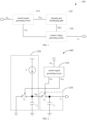
- FIG. 1 is a structural schematic view of a frequency-detecting circuit according to a first embodiment of the present disclosure.
- the frequency-detecting circuit 100 includes a control-signal generating circuit 110, a charging and discharging path 120, and a control-voltage generating circuit 130.
- the control-signal generating circuit 110 is configured to receive a to-be-detected clock signal CK in and generate a first control signal CK P corresponding to the to-be-detected clock signal CK in and a second control signal CK PD delayed relative to the first control signal CK P .
- the charging and discharging path 120 is coupled to the control-signal generating circuit 110, and performs a charging process or a discharging process under control of the second control signal CK PD .
- the charging and discharging path 120 performs the discharging process, and the charging and discharging path 120 performs the charging process during another period when the second control signal CK PD is at a low level.
- the control-voltage generating circuit 130 is coupled to an output terminal of the charging and discharging path 120 and the control-signal generating circuit 110, and configured to sample values of a voltage signal ND1 of an output terminal of the charging and discharging path 120 before the discharging process during a period with a pulse width when the first control signal CK P is at the high level, to output a first voltage signal V 1 .
- a frequency of the second control signal CK PD is the same as the frequency of the to-be-detected clock signal CK in , and the pulse width during which the second control signal CK PD is at the high level remains unchanged. Therefore, a discharging period of the charging and discharging path 120 in a clock cycle of the second control signal CK PD is fixed, and a charging period of the charging and discharging path 120 is determined by a length of the second control signal CK PD being at the low level, therefore, the charging period of the charging and discharging path 120 is determined by a cycle length of the second control signal CK PD .
- the voltage value of the voltage signal ND1 of the output terminal of the charging and discharging path 120 may reflect a magnitude of the frequency of the to-be-detected clock signal CK in .
- the control-voltage generating circuit 130 further samples the voltage signal ND1 during the period with the pulse width when the first control signal CK P is at the high level and outputs a sampled voltage signal as the first voltage signal V 1 . Since a high-level pulse of the first control signal CK P is earlier than a high-level pulse of the second control signal CK PD , a sampling time point being before the discharging process of each cycle of the charging and discharging path 120 may be guaranteed.
- the sampled voltage signal reflects a voltage value reached in each charging process, and is output as the first voltage signal V 1 .
- a magnitude of the first voltage signal V 1 reflects a magnitude of the cycle length (i.e., the frequency) of the second control signal CK PD , i.e., the first voltage signal V 1 reflects the frequency of the to-be-detected clock signal CK in .
- the frequency-detecting circuit includes the control-signal generating circuit, the charging and discharging path, and the control-voltage generating circuit.
- the control-signal generating circuit is configured to receive the to-be-detected clock signal and generate the first control signal corresponding to the to-be-detected clock signal and the second control signal delayed relative to the first control signal;
- the charging and discharging path is coupled to the control-signal generating circuit, and performing the charging process or a discharging process under the control of the second control signal, during the period with the pulse width when the second control signal is at the high level, the charging and discharging path performs the discharging process, and the charging and discharging path performs the charging process during another period when the second control signal is at the low level;
- the control-voltage generating circuit is coupled to the output terminal of the charging and discharging path and the control-signal generating circuit, and configured to sample values of the voltage of the output terminal of the charging and discharging path before
- the corresponding voltage signal is generated based on the frequency of the clock signal, so as to correspondingly determine the magnitude of the frequency of the clock signal through detecting the voltage value of the voltage signal. Further, in some scenarios where the accurate frequency of the clock signal is not required to be acquired and only the magnitude of the frequency needs to be determined, the magnitude of the frequency of the clock signal may be directly reflected through determining the magnitude of the voltage value of the generated voltage signal. In addition, the voltage signal may be directly configured as the input of the subsequent circuit to indicate the frequency of the clock signal.
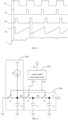
- FIG. 2 is a structural schematic view of the frequency-detecting circuit according to a second embodiment of the present disclosure.
- the frequency-detecting circuit 100 includes the control-signal generating circuit 110, the charging and discharging path 120, and the control-voltage generating circuit 130.
- the control-signal generating circuit 110 is configured to receive the to-be-detected clock signal CK in and generate the first control signal CK P corresponding to the to-be-detected clock signal CK in and the second control signal CK PD delayed relative to the first control signal CK P .
- the charging and discharging path 120 is coupled to the control-signal generating circuit 110, and performs the charging process or the discharging process under the control of the second control signal CK PD .
- the charging and discharging path 120 performs the discharging process, and the charging and discharging path 120 performs the charging process during another period when the second control signal CK PD is at the low level.
- the control-voltage generating circuit 130 is coupled to the output terminal of the charging and discharging path 120 and the control-signal generating circuit 110, and configured to sample values of the voltage signal ND1 of the output terminal of the charging and discharging path 120 before the discharging process during the period with the pulse width when the first control signal CK P is at the high level, to output the first voltage signal V 1 .
- the charging and discharging path 120 further includes a power supply A, a first switch S 1 and a first capacitor C 1 .
- a first terminal of the first capacitor C 1 is coupled to the power supply A, and a second terminal of the first capacitor C 1 is grounded.
- a first terminal of the first switch S 1 is coupled to the first terminal of the first capacitor C 1 , a second terminal of the first switch S 1 is grounded, and a control terminal of the first switch S 1 inputs the second control signal CK PD .
- the control-voltage generating circuit 130 further includes a second switch S 2 and a second capacitor C 2 .
- a first terminal of the second switch S 2 is coupled to the first terminal of the first capacitor C 1 (i.e., the output terminal ND1 of the charging and discharging path 120), and a control terminal of the second switch S 2 inputs the first control signal CK P .
- a first terminal of the second capacitor C 2 is coupled to a second terminal of the second switch S 2 and configured to output the first voltage signal V 1 , and a second terminal of the second capacitor C 2 is grounded.
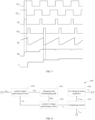
- FIG. 3 is a schematic view of a waveform of a signal at each node according to the second embodiment of the present disclosure.
- the first switch S 1 and the second switch S 2 are turned on when control terminals thereof are at a logic high level "1", and turned off when the control terminals thereof are at a logic low level "0".
- a pulse width when the first control signal CK P is the logic high level “1” and a pulse width when the second control signal CK PD is the logic high level “1” are fixed (a method for fixing the pulse width will be described in the following).
- a length of a period when the first control signal CK P is the logic low level “0” is determined by the cycle length of the first control signal CK P .
- the length of the period when the second control signal CK PD is the logic low level "0” is determined by the cycle length of the second control signal CK PD .
- both the first control signal CK P and the second control signal CK PD are generated by processing the to-be-detected clock signal CK in , both the first control signal CK P and the second control signal CK PD have the same cycle with the to-be-detected clock signal CK in Therefore, a period of the power supply A charging for the first capacitor C 1 is determined by the cycle (or frequency) of the to-be-detected clock signal CK in . The less the frequency of the to-be-detected clock signal CK in is, the greater the cycle is, the greater the period of the power supply A charging for the first capacitor C 1 is.
- the second switch S 2 When the first control signal CK P is the logic low level “0" and the second control signal CK PD is the logic high level “1”, the second switch S 2 is turned off, the first switch S 1 is turned on, the first capacitor C 1 is discharged, and the second capacitor C 2 is maintained.
- the voltage of the first node signal ND 1 is decreased, and the first voltage signal V 1 is maintained.
- the first capacitor C 1 After multiple clock cycles, the first capacitor C 1 is charged and discharged cyclically, the voltage of the first node signal ND 1 has the saw tooth shape.
- the second capacitor C 2 is charged multiple times, and the first voltage signal V 1 is increased through a charge share between the first capacitor C 1 and the second capacitor C 2 .
- the stable voltage value may reflect a value reached in each charging cycle of the first node signal ND 1 , that is, the stable voltage value may reflect the magnitude of the cycle length of the second control signal CK PD , i.e., the magnitude of the frequency of the to-be-detected clock signal CK in .
- FIG. 4 is a structural schematic view of the frequency-detecting circuit according to a third embodiment of the present disclosure.
- the frequency-detecting circuit 100 includes the control-signal generating circuit 110, the charging and discharging path 120, and the control-voltage generating circuit 130.
- the control-signal generating circuit 110 is configured to receive the to-be-detected clock signal CK in and generate the first control signal CK P corresponding to the to-be-detected clock signal CK in and the second control signal CK PD delayed relative to the first control signal CK P .
- the charging and discharging path 120 is coupled to the control-signal generating circuit 110, and performs the charging process or the discharging process under the control of the second control signal CK PD .
- the charging and discharging path 120 performs the discharging process, and the charging and discharging path 120 performs the charging process during another period when the second control signal CK PD is at the low level.
- the control-voltage generating circuit 130 is coupled to the output terminal of the charging and discharging path 120 and the control-signal generating circuit 110, and configured to sample values of the voltage signal ND1 of the output terminal of the charging and discharging path 120 before the discharging process during the period with the pulse width when the first control signal CK P is at the high level, to output the first voltage signal V 1 .
- the charging and discharging path 120 further includes a power supply A, a first switch S 1 and a first capacitor C 1 .
- a first terminal of the first capacitor C 1 is coupled to the power supply, and a second terminal of the first capacitor C 1 is grounded.
- a first terminal of the first switch S 1 is coupled to the first terminal of the first capacitor C 1 , a second terminal of the first switch S 1 is grounded, and a control terminal of the first switch S 1 inputs the second control signal CK PD .
- the control-voltage generating circuit 130 further includes a second switch S 2 and a second capacitor C 2 , a third switch S 3 and a third capacitor C 3 .
- the first terminal of the second switch S 2 is coupled to the first terminal of the first capacitor C 1 (i.e., the output terminal of the charging and discharging path 120), and the control terminal of the second switch S 2 inputs the first control signal CK P .
- the first terminal of the second capacitor C 2 is coupled to the second terminal of the second switch S 2 , and the second terminal of the second capacitor C 2 is grounded.
- a first terminal of the third switch S 3 is coupled to the first terminal of the second capacitor C 2 , and a control terminal of the third switch inputs the second control signal CK PD .
- a first terminal of the third capacitor C 3 is coupled to a second terminal of the third switch S 3 and configured to output the first voltage signal V 1 , and a second terminal of the third capacitor C 3 is grounded.
- a third switch S 3 and a third capacitor C 3 are further added, and the first terminal of the third capacitor C 3 is configured as the output terminal of the first voltage signal V 1 .
- FIG. 5 is a schematic view of the waveform of the signal at each node according to the third embodiment of the present disclosure.
- the first switch S 1 , the second switch S 2 , and the third switch S 3 are turned on when control terminals thereof are at the logic high level "1", and turned off when the control terminals thereof are at the logic low level "0".
- the second switch S 2 When the first control signal CK P is the logic high level “1" and the second control signal CK PD is the logic low level “0”, the second switch S 2 is turned on, the first switch S 1 and the third switch S 3 are turned off, and the power supply A charges for the first capacitor C 1 and the second capacitor C 2 , the voltage of the first node signal ND 1 and a voltage of a second node signal ND 2 are increased.
- the first control signal CK P is the logic high level "1” and the second control signal CK PD is the logic low level "0”
- the power supply A continues to charge for the first capacitor C 1 . It can be seen that the charging period of the first capacitor C 1 is determined by the length of the period when the second control signal CK PD is the logic low level "0".
- the length of the period when the first control signal CK P is the logic low level “0” is determined by the cycle length of the first control signal CK P .
- the length of the period when the second control signal CK PD is the logic low level “0” is determined by the cycle length of the second control signal CK PD .
- both the first control signal CK P and the second control signal CK PD are generated by processing the to-be-detected clock signal CK in , both the first control signal CK P and the second control signal CK PD have the same cycle with the to-be-detected clock signal CK in . Therefore, the period of the power supply A charging for the first capacitor C 1 is determined by the cycle (or frequency) of the to-be-detected clock signal CK in . The less the frequency of the to-be-detected clock signal CK in is, the greater the cycle is, the greater the period of the power supply A charging for the first capacitor C 1 is.
- the second switch S 2 When the first control signal CK P is the logic low level “0" and the second control signal CK PD is the logic high level “1”, the second switch S 2 is turned off, the first switch S 1 and the third switch S 3 are turned on, the first capacitor C 1 is discharged, the second capacitor C 2 is maintained, and the third capacitor C 3 is charged.
- the voltage of the first node signal ND 1 is decreased, the voltage of the second node signal ND 2 is maintained, and the first voltage signal V 1 is increased.
- the first capacitor C 1 After the multiple clock cycles, the first capacitor C 1 is charged and discharged cyclically, the voltage of the first node signal ND 1 has the saw tooth shape.
- the second capacitor C 2 is charged multiple times, and the voltage of the second node signal ND 2 is increased through the charge share between the first capacitor C 1 and the second capacitor C 2 .
- the third capacitor C 3 is charged multiple times, the first voltage signal V 1 is increased through a charge share between the third capacitor C 3 and the second capacitor C 2 , and finally reached a stable voltage value (Under the condition that the frequency of the to-be-detected clock signal CK in is stable).
- the stable voltage value may reflect the value reached in each charging cycle of the first node signal ND 1 , that is, the stable voltage value may reflect the magnitude of the cycle length of the second control signal CK PD , i.e., the magnitude of the frequency of the to-be-detected clock signal CK in .
- the third capacitor C 3 is added on the basis of the second embodiment. It can be seen from FIG.5 that a voltage effect of the first voltage signal V 1 is better than that of the second node signal ND 2 .
- FIG. 6 is a structural schematic view of the frequency-detecting circuit according to a fourth embodiment of the present disclosure.
- the frequency-detecting circuit 100 includes the control-signal generating circuit 110, the charging and discharging path 120, and the control-voltage generating circuit 130.
- control-signal generating circuit 110 may include a first AND gate unit A 1 , a first delay unit D 1 , a first inversion unit N 1 (non-gate unit), a second AND gate unit A 2 , and a second delay unit D 2 .
- a first terminal of the first AND gate unit A 1 inputs the to-be-detected clock signal CK in , and a second terminal of the first AND gate unit A 1 inputs an enable signal EN (being the logic high level "1" during operating).
- An input terminal of the first delay unit D 1 is coupled to an output terminal of the first AND gate unit A 1 (In some embodiments, the control-signal generating circuit 110 may not include the first AND gate unit A 1 , and the input terminal of the first delay unit D 1 is directly connected to the to-be-detected clock signal CK in ).
- An input terminal of the first inversion unit N 1 is coupled to the output terminal of the first delay unit D 1 .
- a first input terminal of the second AND gate unit A 2 is coupled to the input terminal of first delay unit D 1
- a second input terminal of the second AND gate unit A 2 is coupled to an output terminal of the first inversion unit N 1
- an output terminal of the second AND gate unit A 2 outputs the first control signal CK P .
- An input terminal of the second delay unit D 2 is coupled to the output terminal of the second AND gate unit, and an output terminal of the second delay unit D 2 outputs the second control signal CK PD .
- the charging and discharging path 120 further includes the power supply A, the first switch S 1 and the first capacitor C 1 .
- the first terminal of the first capacitor C 1 is coupled to the power supply, and the second terminal of the first capacitor C 1 is grounded.
- the first terminal of the first switch S 1 is coupled to the first terminal of the first capacitor C 1 , the second terminal of the first switch S 1 is grounded, and the control terminal of the first switch S 1 inputs the second control signal CK PD .
- the control-voltage generating circuit 130 further includes the second switch S 2 and the second capacitor C 2 , the third switch S 3 and the third capacitor C 3 .
- the first terminal of the second switch S 2 is coupled to the first terminal of the first capacitor C 1 (i.e., the output terminal of the charging and discharging path 120), and the control terminal of the second switch S 2 inputs the first control signal CK P .
- the first terminal of the second capacitor C 2 is coupled to the second terminal of the second switch S 2 , and the second terminal of the second capacitor C 2 is grounded.
- the first terminal of the third switch S 3 is coupled to the first terminal of the second capacitor C 2 , and the control terminal of the third switch inputting the second control signal CK PD .
- the first terminal of the third capacitor C 3 is coupled to the second terminal of the third switch S 3 and configured to output the first voltage signal V 1 , and the second terminal of the third capacitor C 3 is grounded.
- the first switch S 1 , the second switch S 2 , and the third switch S 3 are implemented by an nMOS transistor, or a transmission gate formed of an nMOS transistor and a pMOS transistor.
- FIG. 7 is a schematic view of the waveforms of the signal according to the fourth embodiment of the present disclosure.
- the first switch S 1 , the second switch S 2 , and the third switch S 3 are turned on when the control terminals thereof are at the logic high level "1", and turned off when the control terminals thereof are at the logic low level "0".
- a reference clock signal CK ref is obtained after the to-be-detected clock signal CK in is processed by the first delay unit D1 and the first inversion unit N 1 .
- the reference clock signal CK ref is opposite to the to-be-detected clock signal CK in and has a certain delay relative to the to-be-detected clock signal CK in .
- a "AND" logic process may be performed for the to-be-detected clock signal CK in and the reference clock signal CK ref , and the first control signal CK P may be obtained. In this way, both the cycle length of the first control signal CK P and the cycle length of the second control signal CK PD are the same with a cycle length of the to-be-detected clock signal CK in .
- the pulse width when the first control signal CK P is the logic high level "1" and the pulse width when the second control signal CK PD is the logic high level "1" are fixed, which both are determined the first delay unit D 1 .
- the second switch S 2 When the first control signal CK P is the logic high level “1" and the second control signal CK PD is the logic low level “0”, the second switch S 2 is turned on, the first switch S 1 and the third switch S 3 are turned off, and the power supply A charges for the first capacitor C 1 and the second capacitor C 2 , the voltage of the first node signal ND 1 and a voltage of a second node signal ND 2 are increased.
- the first control signal CK P is the logic high level "1” and the second control signal CK PD is the logic low level "0”
- the power supply A continues to charge for the first capacitor C 1 . It can be seen that the charging period of the first capacitor C 1 is determined by the length of the period when the second control signal CK PD is the logic low level "0".
- the pulse width when the first control signal CK P is the logic high level “1” and the pulse width when the second control signal CK PD is the logic high level “1” are fixed.
- the length of the period when the first control signal CK P is the logic low level “0” is determined by the cycle length of the first control signal CK P .
- the length of the period when the second control signal CK PD is the logic low level “0” is determined by the cycle length of the second control signal CK PD .
- both the first control signal CK P and the second control signal CK PD are generated by processing the to-be-detected clock signal CK in , both the first control signal CK P and the second control signal CK PD have the same cycle with the to-be-detected clock signal CK in Therefore, the period of the power supply A charging for the first capacitor C 1 is determined by the cycle (or frequency) of the to-be-detected clock signal CK in . The less the frequency of the to-be-detected clock signal CK in is, the greater the cycle is, the greater the period of the power supply A charging for the first capacitor C 1 is.
- the second switch S 2 When the first control signal CK P is the logic low level “0" and the second control signal CK PD is the logic high level “1”, the second switch S 2 is turned off, the first switch S 1 and the third switch S 3 are turned on, the first capacitor C 1 is discharged, the second capacitor C 2 is maintained, and the third capacitor C 3 is charged.
- the voltage of the first node signal ND 1 is decreased, the voltage of the second node signal ND 2 is maintained, and the first voltage signal V 1 is increased.
- the first capacitor C 1 After the multiple clock cycles, the first capacitor C 1 is charged and discharged cyclically, the voltage of the first node signal ND 1 has the saw tooth shape.
- the second capacitor C 2 is charged multiple times, and the voltage of the second node signal ND 2 is increased through the charge share between the first capacitor C 1 and the second capacitor C 2 .
- the third capacitor C 3 is charged multiple times, the first voltage signal V 1 is increased through the charge share between the third capacitor C 3 and the second capacitor C 2 , and finally reached the stable voltage value (Under the condition that the frequency of the to-be-detected clock signal CK in is stable).
- the stable voltage value may reflect the value reached in each charging cycle of the first node signal ND 1 , that is, the stable voltage value may reflect the magnitude of the cycle length of the second control signal CK PD , i.e., the magnitude of the frequency of the to-be-detected clock signal CK in .
- the third capacitor C 3 is added on the basis of the second embodiment. It can be seen from FIG.7 that the voltage effect of the first voltage signal V 1 is better than that of the second node signal ND 2 .
- FIG. 8 is a structural schematic view of the frequency-detecting circuit according to a fifth embodiment of the present disclosure.
- the frequency-detecting circuit 100 includes the control-signal generating circuit 110, the charging and discharging path 120, the control-voltage generating circuit 130, a comparing circuit 140, and a low-dropout linear regulator 150.
- control-signal generating circuit 110 is configured to receive the to-be-detected clock signal CK in and generate the first control signal CK P corresponding to the to-be-detected clock signal CK in and the second control signal CK PD delayed relative to the first control signal CK P .
- the charging and discharging path 120 is coupled to the control-signal generating circuit 110, and performs the charging process or the discharging process under the control of the second control signal CK PD .
- the charging and discharging path 120 performs the discharging process, and the charging and discharging path 120 performs the charging process during another period when the second control signal CK PD is at the low level.
- the control-voltage generating circuit 130 is coupled to the output terminal of the charging and discharging path 120 and the control-signal generating circuit 110, and configured to sample values of the voltage signal ND1 of the output terminal of the charging and discharging path 120 before the discharging process during the period with the pulse width when the first control signal CK P is at the high level, to output the first voltage signal V 1 .
- the less the frequency of the to-be-detected clock signal CK in is, the greater the voltage value of the first voltage signal V 1 is.
- the comparing circuit 140 is coupled to the control-voltage generating circuit, and configured to compare the voltage value of the first voltage signal with a voltage value of at least one preset reference-voltage signal V ref , to obtain a corresponding comparing-result signal V comp .
- the low-dropout linear regulator 150 is coupled to an output terminal of the comparing circuit 140 and configured to generate a matched second voltage signal V 2 according to the comparing-result signal V comp .
- the frequency value of the to-be-detected clock signal CK in is negatively correlated with a voltage value of the first voltage signal V 1 . That is, the less the frequency value of the to-be-detected clock signal CK in , the greater the voltage value of the first voltage signal V 1 .
- the comparing circuit 140 may adopt a hysteresis comparator, a non-inverting input terminal of the hysteresis comparator inputs the reference voltage signal V ref , and an inverting input terminal of the hysteresis comparator inputs the first voltage signal V 1 .
- Adopting the hysteresis comparator may avoid a problem that the comparing circuit 140 flips back and forth due to a jitter of a frequency of the to-be-detected clock signal CK in .
- the comparing circuit 140 may also be implemented by adopting comparators of other types.
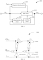
- FIG. 9 is a structural schematic view of a delay-locked circuit according to an embodiment of the present disclosure.
- the delay-locked circuit 900 includes a delay circuit 910, a phase-detecting circuit 920, a controlling circuit 930, and the frequency-detecting circuit 100 described in the above embodiments.
- FIG. 10 is a structural schematic view of the delay circuit 910 according to an embodiment of the present disclosure.
- the delay circuit 910 includes a delay line.
- Each operation of adjusting of the delay circuit 910 is achieved by changing control signals D 0 , D 1 ??D n (only D 0 and D 1 are shown in FIG. 10 for a simplicity) to adjust the number of gate circuits accessed to the delay line, such that a total delay of a second clock signal CK out relative to a first clock signal CK in (i.e., the to-be-detected clock signal CK in ) may be adjusted, and adjusting step by step until an edge of the first clock signal CK in may be aligned to an edge of the second clock signal CK out (i.e., locked).
- the control signal D 0 is 0, and the first clock signal CK in only passes through a first delay path formed by the two leftmost NOT-AND (NAND) gates (i.e., an NAND gate 1 and an NAND gate 2) and is output as the second clock signal CK out .
- NAND NOT-AND
- the control signal D 0 is changed to be 1
- the control signal D 1 is 0.
- the first clock signal CK in passes through a second delay path formed by four NAND gates (i.e., the NAND gate 1, the NAND gate 2, an NAND gate 3, and an NAND gate 4) and is output as the second clock signal CK out ......, and so on.
- the delay path may be changed until the total delay generated by the delay line allow the edge of the first clock signal CK in to be aligned to the edge of the first clock signal CK in (i.e., locked).
- the structure of the delay circuit 910 in FIG. 10 is only an example, and the delay line may also be implemented by other gate circuits. It can be seen that an adjusting amount (i.e., a length of each operation) of the delay in each operation of the delay line is related to a delay generated by a single gate circuit. The delay of the single gate circuit is adjusted by adjusting a voltage of the power supply in the above embodiments described with reference to FIG. 9 .
- the frequency-detecting circuit 100 in FIG. 8 may not include the low-dropout linear regulator 150.
- a delaying device may be added to each delay node of each delay path of the delay line, the delay device may be an MOS capacitor 1, ......, or an MOS capacitor n shown in FIG. 10 (only the MOS capacitor 1 and the MOS capacitor 2 are shown in FIG. 10 for the simplicity).
- the MOS capacitors are turned on or off in response to a logic level of the comparing result signal V comp , thereby adjusting the delay of each delay path of the delay line, i.e., the delay (i.e., the length of each operation) of the delay line in each operation of adjusting.
- the comprising result signal V comp controls the MOS capacitor of each delay node to be turned on, such that both the delay of the first delay path and the delay of the second delay path are increased correspondingly, and thereby increasing the delay (i.e., the length of each operation) of the delay line in each operation of adjusting.
- the comprising result signal V comp controls the MOS capacitor of each delay node to be turned off, such that both the delay of the first delay path and the delay of the second delay path are reduced correspondingly, and thereby reducing the delay (i.e., the length of each operation) of the delay line in each operation of adjusting.
- a principle of an MOS tube forming the capacitor is that a gate oxide layer between a gate and a channel is configured as an insulating medium, the gate is configured as an upper electrode plate, and three terminals (i.e., a source, a drain, and a substrate) are electrically connected together to form a lower electrode plate.
- the frequency-detecting circuit includes the control-signal generating circuit, the charging and discharging path, and the control-voltage generating circuit.
- the control-signal generating circuit is configured to receive the to-be-detected clock signal and generate the first control signal corresponding to the to-be-detected clock signal and the second control signal delayed relative to the first control signal;
- the charging and discharging path is coupled to the control-signal generating circuit, and performing the charging process or a discharging process under the control of the second control signal, during the period with the pulse width when the second control signal is at the high level, the charging and discharging path performs the discharging process, and the charging and discharging path performs the charging process during another period when the second control signal is at the low level;
- the control-voltage generating circuit is coupled to the output terminal of the charging and discharging path and the control-signal generating circuit, and configured to sample values of the voltage of the output terminal of the charging and discharging path before
- the corresponding voltage signal is generated based on the frequency of the clock signal, so as to correspondingly determine the magnitude of the frequency of the clock signal through detecting the voltage value of the voltage signal. Further, in some scenarios where the accurate frequency of the clock signal is not required to be acquired and only the magnitude of the frequency needs to be determined, the magnitude of the frequency of the clock signal may be directly reflected through determining the magnitude of the voltage value of the generated voltage signal. In addition, the voltage signal may be directly configured as the input of the subsequent circuit to indicate the frequency of the clock signal.
- the first voltage signal V 1 output by the frequency-detecting circuit above may be applied to multiple application scenarios requiring the frequency of the to-be-detected clock signal CK in changing.
- the first voltage signal V 1 may be applied to a DCC.
- FIG. 11 is a structural schematic view of a DCC according to an embodiment of the present disclosure.
- the DCC 800 includes a filtering circuit 810, a DC bias amplifying circuit 830, and an attenuation adjusting circuit 840.
- an input terminal of the filtering circuit 810 is configured to input a first clock signal CK in .
- An input terminal of the DC bias amplifying circuit 830 is coupled to an output terminal of the filtering circuit 810, and an output terminal of the DC bias amplifying circuit 830 is configured to output a second clock signal CK out .
- An input terminal of the attenuation adjusting circuit 840 is coupled to the input terminal of the filtering circuit 810, and an output terminal of the attenuation adjusting circuit 840 is coupled to the input terminal of the DC bias amplifying circuit 830.
- the attenuation adjusting circuit 840 includes the frequency-detecting circuit described above, as shown in FIG.11 .
- the first clock signal CK in is as the to-be-detected clock signal CK in in FIG.1 .
- the attenuation adjusting circuit 840 performs an attenuation adjusting process for a signal output by the filtering circuit 810 based on a frequency of the first clock signal CK in . In an embodiment, the less the frequency of the first clock signal CK in is, the greater a corresponding attenuation amplitude is.
- the DCC does not include the attenuation adjusting circuit 840.
- Components of the first clock signal CK in after being processed by the filtering circuit 810 also include a low-frequency component having a greater ratio and a greater signal amplitude.
- the low-frequency component having the greater ratio may have an influence on a DC bias point of the DC bias amplifying circuit 830 in a subsequent level, which may deteriorate a DCC correcting capability.
- FIG. 12 is a schematic view of changes of duty cycles of a first clock signal and a second clock signal without an attenuation process.
- Different curves in FIG. 12 correspond to first clock signals CK in of different frequencies. It can be seen that the greater the frequency of the first clock signal CK in is, the closer to an ideal value 50% the duty cycle of the second clock signal CK out obtained after a converting process is. On the contrary, the less the frequency of the first clock signal CK in is, the greater a difference between the duty cycle of the second clock signal CK out obtained after the converting process and the ideal value 50% is, which is not expected.
- the attenuation adjusting circuit 840 is added.
- the attenuation adjusting circuit 840 is configured to perform the attenuation adjusting process for the signal output by the filtering circuit 810 based on the frequency of the first clock signal CK in , and the less the frequency of the first clock signal CK in is, the greater the corresponding attenuation amplitude is.
- an amplitude of the low-frequency component of a signal input into the DC bias amplifying circuit 830 may be reduced, and the influence of the low-frequency component on the DC bias point of the DC bias amplifying circuit 830 in the subsequent level may be reduced.
- the greater the frequency of the first clock signal CK in is, the less the corresponding attenuation amplitude is, which will not cause much influence on an original circuit.
- FIG. 13 is a schematic view of the changes of the duty cycles of the first clock signal and the second clock signal after the attenuation process. Different curves in FIG.13 correspond to the first clock signals CK in of the different frequencies. Comparing FIG. 12 with FIG. 13 , the greater the frequency of the first clock signal CK in is, the closer to the ideal value 50% the duty cycle of the second clock signal CK out obtained after the converting process is. However, when the frequency of the first clock signals CK in becomes less, the difference between the duty cycle of the second clock signal CK out obtained after the converting process and the ideal value 50% is reduced relative to FIG. 12 , i.e., closer to the ideal value 50% than FIG. 12 .
- FIG. 14 is a structural schematic view of the DCC according to another embodiment of the present disclosure.
- the DCC includes the filtering circuit 810, the DC bias amplifying circuit 830, and the attenuation adjusting circuit 840.
- the attenuation adjusting circuit 840 includes the frequency-detecting circuit 100 described in the above embodiments.
- the attenuation adjusting circuit 840 further includes an adjustable resistance device 820.
- a first terminal of the adjustable resistance device 820 is coupled to the output terminal of the filtering circuit 810, a second terminal of the adjustable resistance device 820 is coupled to the input terminal of the DC bias amplifying circuit 830, and the greater an on-resistance of the adjustable resistance device 820, the less a DC component of a signal V out of the input terminal of the DC bias amplifying circuit 830.
- An input terminal of the frequency-detecting circuit 100 is coupled to the input terminal of the filtering circuit 810, and an output terminal of the frequency-detecting circuit 100 is coupled to a control terminal of the adjustable resistance device 820.
- the first voltage signal V 1 is generated by the frequency-detecting circuit based on the frequency of the first clock signal CK in , the control terminal of the adjustable resistance device is configured to input the first voltage signal, and the on-resistance of the adjustable resistance device 820 changes in response to a voltage value of the first voltage signal V 1 changing.
- the frequency-detecting circuit 100 generates the corresponding first voltage signal V 1 based on a frequency of the first clock signal CK in , the on-resistance of the adjustable resistance device 820 changes in response to a voltage value of the first voltage signal V 1 changing.
- V out R out R in + R out ⁇ V in
- R in is the on-resistance of the adjustable resistance device 820
- R out is a total resistance of N numbers of resistors R 0 connected in series in the DC bias amplifying circuit 830 (as shown in the following description about FIG. 15 for details).
- the first clock signal CK in in a low frequency adjusting the duty cycle of the second clock signal CK out output by the DCC 800 may be achieved.
- FIG. 15 is a structural schematic view of the DCC according to a yet embodiment of the present disclosure.
- the DCC 800 includes the filtering circuit 810, the DC bias amplifying circuit 830, and the attenuation adjusting circuit 840.
- the attenuation adjusting circuit 840 includes the frequency-detecting circuit 100 described in the above embodiments.
- the attenuation adjusting circuit 840 further includes the adjustable resistance device 820.
- the first terminal of the adjustable resistance device 820 is coupled to the output terminal of the filtering circuit 810, the second terminal of the adjustable resistance device 820 is coupled to the input terminal of the DC bias amplifying circuit 830, and the greater an on-resistance of the adjustable resistance device 820, the less the DC component of the signal V out of the input terminal of the DC bias amplifying circuit 830.
- the input terminal of the frequency-detecting circuit 100 is coupled to the input terminal of the filtering circuit 810, and the output terminal of the frequency-detecting circuit 100 is coupled to the control terminal of the adjustable resistance device 820.
- the first voltage signal V 1 is generated by the frequency-detecting circuit based on the frequency of the first clock signal CK in , the control terminal of the adjustable resistance device is configured to input the first voltage signal, and the on-resistance of the adjustable resistance device 820 changes in response to the voltage value of the first voltage signal V 1 changing.
- the adjustable resistance device 820 is a transmission gate unit.
- the transmission gate unit includes an nMOS transistor and a pMOS transistor. A first terminal of the nMOS transistor is coupled to the output terminal of the filtering circuit 810, a second terminal of the nMOS transistor is coupled to the input terminal of the DC bias amplifying circuit 830, and a control terminal of the nMOS transistor is coupled to the output terminal of the frequency-detecting circuit 100.
- a first terminal of the pMOS transistor is coupled to the output terminal of the filtering circuit 810, a second terminal of the pMOS transistor is coupled to the input terminal of the DC bias amplifying circuit 830, and a control terminal of the pMOS transistor is coupled to the output terminal of the frequency-detecting circuit 100.
- FIG. 16 is a diagram showing a relationship between an on-resistance and a control-terminal voltage of a transmission gate according to some embodiments of the present disclosure. It can be seen from FIG. 16 that when a control-terminal voltage of the transmission gate (i.e., a gate voltage of the nMOS transistor and a gate voltage of the pMOS transistor) is a threshold voltage V 0 , a resistance of the transmission gate is the greatest. When the control-terminal voltage is decreased or increased on the basis of V 0 , the resistance of the transmission gate gradually decreases. Therefore, in this embodiment, a changing range of the first voltage signal V 1 output by the frequency-detecting circuit 100 may be controlled to be between 0-V 0 , such that the resistance of the transmission gate may increase with the first voltage signal V 1 increasing.
- a control-terminal voltage of the transmission gate i.e., a gate voltage of the nMOS transistor and a gate voltage of the pMOS transistor
- V 0 a threshold voltage of the
- the filtering circuit 810 includes a low-pass filtering circuit and a high-pass filtering circuit.
- An input terminal of the low-pass filtering circuit is configured to input the first clock signal CK in
- an input terminal of the high-pass filtering circuit is coupled to an output terminal of the low-pass filtering circuit
- an output terminal of the high-pass filtering circuit is coupled to the input terminal of the DC bias amplifying circuit 830.
- the low-pass filtering circuit is configured to filter the low-frequency component in the signal.
- the low-pass filtering circuit includes a first resistor R 1 and a fourth capacitor C 4 .
- a first terminal of the first resistor R 1 is configured to input the first clock signal CK in .
- a first terminal of the fourth capacitor C 4 is coupled to a second terminal of the first resistor R 1 , and a second terminal of the fourth capacitor C 4 is grounded.
- the high-pass filtering circuit is configured to filter a high-frequency component in the signal.
- the high-pass filtering circuit includes a fifth capacitor C 5 and a sixth capacitor C 6 .
- a first terminal of the fifth capacitor C 5 is coupled to the second terminal of the fourth capacitor C 4
- a second terminal of the fifth capacitor C 5 is coupled to the input terminal of the DC bias amplifying circuit 830.
- a first terminal of the sixth capacitor C 6 is coupled to the second terminal of the fifth capacitor C 5 , and a second terminal of the sixth capacitor C 6 is grounded.
- the DC bias amplifying circuit 830 includes an inverting unit group, a resistance unit group, and a capacitor group.
- the inverting unit group includes N numbers of inverting units N 0 , the N numbers of inverting units N 0 are connected in series in sequence, and an input terminal of the first inverting unit N 0 in the N numbers of inverting units N 0 is coupled to the output terminal of the filtering circuit 810.
- An output terminal of the last inverting unit N 0 in the N numbers of inverting units N 0 is configured to output the second clock signal CK out .
- the resistance unit group includes N numbers of resistors R 0 , the N numbers of resistors R 0 are connected in series in sequence, and the resistance unit group and the inverting unit group are connected in parallel.
- the capacitor group includes N-1 numbers of capacitors C 0 , a first terminal of each capacitor C 0 of the N-1 numbers of capacitors C 0 is sequentially coupled between two adjacent resistors R 0 of the N numbers of resistors R 0 , and a second terminal of each capacitor C 0 of the N-1 numbers of capacitors C 0 is grounded.
- N is an odd number greater than 3.
- the DCC 800 further includes a second inverting unit N 2 , an input terminal of the second inverting unit N 2 is coupled to the output terminal of the last inverting unit N 0 in the N inverting units N 0 , and an output terminal of the second inverting unit N 2 is configured to output the second clock signal CK out .
- multiple inverting units are inversely shaped step by step, and multiple RC units (including R 0 and C 0 ) provide the DC bias point.
- the DCC 800 further includes a first buffer unit H 1 and a second buffer unit H 2 , an input terminal of the first buffering unit H 1 is configured to input the first clock signal CK in , and an output terminal of the first buffering unit H 1 is coupled to the input terminal of the filtering circuit 810.
- An input terminal of the second buffering unit H 2 is coupled to the output terminal of the DC bias amplifying circuit 830, and an output terminal of the second buffering unit H 2 is configured to output the second clock signal CK out .
- the DCC provided in the embodiments of the present disclosure includes the filter circuit, the DC bias amplifying circuit, and then attenuation adjusting circuit.
- the input terminal of the filtering circuit is configured to input the first clock signal.
- the input terminal of the DC bias amplifying circuit is coupled to the output terminal of the filtering circuit, and the output terminal of the DC bias amplifying circuit is configured to output the second clock signal.
- the input terminal of the attenuation adjusting circuit is coupled to the input terminal of the filtering circuit, and the output terminal of the attenuation adjusting circuit is coupled to the input terminal of the DC bias amplifying circuit.
- the attenuation adjusting circuit includes the frequency-detecting circuit, and the first clock signal is as the to-be-detected clock signal.
- the attenuation adjusting circuit performs the attenuation adjusting process for the signal output by the filtering circuit based on the frequency of the first clock signal, and the less the frequency of the first clock signal is, the greater the corresponding attenuation amplitude is. Accordingly, when the frequency of the first clock signal input, the attenuation adjusting process is correspondingly performed for an output signal of the filtering circuit, such that an amplitude of a low-frequency DC component of the output signal of the filtering circuit may be attenuated.
- an influence of the low-frequency DC component on the DC bias amplifying circuit may be reduced, which may improve a correcting capability of the duty cycle, such that when the frequency of the input first clock signal is less, the duty cycle of the second clock signal after the duty cycle is adjusted may be close to the ideal value, such as 50%.
- FIG. 17 is a structural schematic view of an electronic device according to an embodiment of the present disclosure.
- the electronic device 500 includes the frequency-detecting circuit 100 in the embodiments described above.
- FIG. 18 is a structural schematic view of a storage device according to an embodiment of the present disclosure.
- the storage device 600 includes a DCC 800.
- the DCC 800 is the same as the DCC provided in the above embodiments, and has a structure and an operating principle similar to those of the DCC provided in the above embodiments, which is not repeated herein.
- the storage device 600 may be the dynamic random access memory (DRAM), such as a DDR (Double Data Rate) SDRAM (Synchronous Dynamic Random-Access Memory).
- DRAM dynamic random access memory
- DDR Double Data Rate
- SDRAM Synchronous Dynamic Random-Access Memory
- the software functional unit may be stored in a computer-readable storage medium.
- a computer software product is stored in a storage medium, including several instructions configured to cause a computer device (which may be a personal computer, a server, or a network device, etc.) or a processor to execute all or a part of operations of the methods described in each embodiment of the present disclosure.
- the above storage medium includes a U disk, a mobile hard disk, a Read-Only Memory (ROM), a Random Access Memory (RAM), a magnetic disk, or an optical disk, and other media capable of storing program codes.
Landscapes
- Physics & Mathematics (AREA)
- Engineering & Computer Science (AREA)
- General Engineering & Computer Science (AREA)
- Computer Hardware Design (AREA)
- Computing Systems (AREA)
- Mathematical Physics (AREA)
- General Physics & Mathematics (AREA)
- Nonlinear Science (AREA)
- Manipulation Of Pulses (AREA)
Claims (15)
- Ein Schaltkreis (100) für das Erkennen von Frequenzen dadurch gekennzeichnet, dass er Folgendes umfasst:Einen Schaltkreis (110) für die Erzeugung eines Steuersignals, der konfiguriert ist, um ein zu erkennendes Taktsignale (CKin) zu empfangen und ein erstes Steuersignal (CKp) zu erzeugen, das dem zu erkennenden Taktsignal (CKin) entspricht, und ein zweites Steuersignal (CKPD), das bezüglich des ersten Steuersignal (CKp) verzögert ist;einen Lade- und Entladepfad (120), der mit dem Schaltkreis (110) für die Erzeugung eines Steuersignals verbunden ist und einen durch das zweite Steuersignal (CKPD) geregelten Lade- oder Entladeverfahren durchführt, wobei während einer Periode mit einer Pulsdauer, wenn das zweite Steuersignal (CKPD) auf einem H-Pegel ist, der Lade- und Entladepfad (120) das Entladeverfahren durchführt, und wobei während einer anderen Periode, wenn das zweite Steuersignal (CKPD) schwach ist, der Lade- und Entladepfad (120) das Ladeverfahren durchführt;
undeinen Schaltkreis (130), der eine Steuerspannung erzeugt und mit einem Ausgabeterminal des Lade- und Entladepfads (120) verbunden ist, und der konfiguriert ist, um Werteproben einer Spannung (NDI) des Ausgabeterminals des Lade- und Entladepfads (120) zu erhalten, bevor das Ladeverfahren ausgeführt wird, während der Periode mit einer Pulsdauer, die dem ersten Steuersignal (CKp) entspricht, wenn dieses stark ist, um ein entsprechendes erste Spannungssignal (V1) auszugeben;wobei der Spannungswert des ersten Spannungssignals (V1) mit einer Frequenz des zu erkennenden Taktsignals (CKin) im Zusammenhang steht. - Der Schaltkreis (100) für das Erkennen von Frequenzen gemäss Anspruch 1, bei dem, je geringer die Frequenz des zu erkennenden Taktsignals (CKin) ist, desdo grösser ist der Spannungswert des ersten Spannungssignals (V1).
- Der Schaltkreis (100) für das Erkennen von Frequenzen gemäss Anspruch 1, bei dem die Frequenz des zweiten Steuersignals (CKPD) dieselbe ist wie die Frequenz des zu erkennenden Taktsignals (CKin) und die Pulsdauer, während der das zweite Steuersignal (CKPD) stark ist unverändert bleibt.
- Der Schaltkreis (100) für das Erkennen von Frequenzen gemäss Anspruch 1, bei dem der Lade- und Entladepfad (120) weiter Folgendes umfasst:Eine Energieversorgung (A);einen ersten Kondensator (C1), ein erstes Terminal des ersten Kondensators (C1), das mit der Energieversorgung (A) verbunden ist, und ein zweites Terminal des ersten Kondensators (C1), das geerdet ist; undeinen ersten Schalter (S1), ein erstes Terminal des ersten Schalters (S1), das mit dem ersten Terminal des ersten Kondensators (C1) verbunden ist, ein zweites Terminal des ersten Schalters (S1), das geerdet ist, und eine Leitstation des ersten Schalters (S1), die das zweite Steuersignal (CKPD) eingibt.
- Der Schaltkreis (100) für das Erkennen von Frequenzen gemäss Anspruch 4, wobei der Schaltkreis (130), der eine Steuerspannung erzeugt, weiter Folgendes umfasst:Einen zweiten Schalter (S2), ein erstes Terminal des zweiten Schalters (S2), das mit dem ersten Terminal des ersten Kondensators (C1) verbunden ist, und eine Leitstation des zweiten Schalters (S2), die das erste Steuersignal (CKp) eingibt; undeinen zweiten Kondensator (C2), ein erstes Terminal des zweiten Kondensators (C2), das mit einem zweiten Terminal des zweiten Schalters (S2) verbunden und konfiguriert ist, um das erste Spannungssignal (V1) auszugeben, und ein zweites Terminal des zweiten Kondensators (C2), das geerdet ist.
- Der Schaltkreis (100) für das Erkennen von Frequenzen gemäss Anspruch 5, wobei der Schaltkreis (130) für das Erzeugen der Steuerspannung weiter Folgendes umfasstEinen dritten Schalter (S3), wobei ein erstes Terminal des dritten Schalters (S3) mit dem ersten Terminal des zweiten Kondensators (C2) verbunden ist, und eine Leitstation des dritten Schalters (S3), die das zweite Stuersignal (CKPD) eingibt; undeinen dritten Kondensator (C3), wobei ein erstes Terminal des dritten Kondensators (C3) mit einem zweiten Terminal des dritten Schalters (S3) verbunden ist und das konfiguriert ist, um das erste Spannungssignal (V1) auszugeben, und wobei ein zweites Terminal des dritten Kondensators (C3) geerdet ist;wobei der erste Schalter (S1), der zweite Schalter (S2) und der dritte Schalter (S3) durch einen nMOS Transistor realisiert werden, oder ein Übertragungsgate, das aus einem nMOS Transistor und einem pMOS Transistor gebildet wird.
- Der Schaltkreis (100) für das Erkennen von Frequenzen gemäss Anspruch 1, wobei der Schaltkreis (110) für das Erzeugen des Steuersignals Folgendes umfasst:Eine erste Verzögerungseinheit (D1), ein Ausgabeterminal der ersten Verzögerungseinheit (D1), das konfiguriert ist, um das zu erkennende Taktsignal (CKin) zu empfangen;eine erste Umkehreinheit (N1), ein Eingabeterminal der ersten Umkehreinheit (N1), das mit dem Ausgabeterminal der ersten Verzögerungseinheit (D1) verbunden ist;eine UND Gateeinheit (A1), ein erstes Eingabeterminal der AND Gateeinheit (A1), konfiguriert, um das zu erkennende Taktsignal (CKin) zu empfangen, ein zweites Eingabeterminal der AND Gateeinheit (A1), verbunden mit einem Ausgabeterminal der ersten Umkehreinheit (N1) und ein Ausgabeterminal der AND Gateeinheit (A1), das das erste Steuersignal (CKp) ausgibt; undeine zweite Verzögerungseinheit (D2), ein Eingabeterminal der zweiten Verzögerungseinheit (D2), die mit dem Ausgabeterminal der AND Gateeinheit (A1) verbunden iat, und ein Ausgabeterminal der zweiten Verzögerungseinheit (D2), das das zweite Steuersignal (CKpd) ausgibt.
- Der Schaltkreis (100) für das Erkennen von Frequenzen gemäss Anspruch 1, der weiter Folgendes umfasst:Einen Vergleichsschaltkreis (140), der mit dem Schaltkreis (130), der die Steuerspannung erzeugt, verbunden und konfiguriert ist, um den Spannungswert des ersten Spannungssignals (V1) mit einem Spannungswert von mindestens einem, voreingestellten Referenzspannungssignal (Vref) zu vergleichen, um ein entsprechendes Vergleichsergebnissignal (Vcomp) zu erhalten; undein Regler (150) für niedrige Abfallspannung, der mit einem Ausgabeterminal des Vergleichsschaltkreises (140) verbunden und konfiguriert ist, um ein abgestimmtes zweites Spannungssignal (V2) übereinstimmend mit dem Vergleichsergebnissignal (Vcomp) zu erzeugen.
- Ein Arbeitszykluskorrektor (DCC) (800) dadurch gekennzeichnet, dass er Folgendes umfasst:Einen Filterungsschaltkreis (810), ein Eingabeterminal für den Filterungsschaltkreis (810), das konfiguriert ist, um das erste Taktsignal (CKin) einzugeben;Einen DCC Schaltkreis (830) für die Verstärkung einer Gleichstromvorspannung, ein Eingabeterminal für den Schaltkreis (830) für die Verstärkung einer Gleichstromvorspannung, das mit einem Ausgabeterminal des Filterungsschaltkreises (810) verbunden ist, und ein Ausgabeterminal des Schaltkreises (830) für die Verstärkung einer Gleichstromvorspannung, der konfiguriert ist, um ein zweites Taktsignal (CKout) auszugeben; undeinen Schaltkreis (840) für die Dämpfunnngseinstellung, ein Eingabeterminal des Schaltkreises (840) für die Dämpfungseinstellung, das mit dem Eingabeterminal des Filterungsschaltkreises (810) verbunden ist, und ein Ausgabeterminal des Schaltkreises (840) für die Dämpfungseinstellung, das mit dem Eingabeterminal des DC Schaltkreises (830) für Vorspannungsverstärkung verbunden ist;dadurch gekennzeichnet, dass der Schaltkreis (840) für die Dämpfungseinstellung einen Schaltkreis (100) für das Erkennen von Frequenzen gemäss irgendeinem der Ansprüche 1-8 umfasst; dass das erste Taktsignal (CKin) wie das zu erkennende Taktsignal (CKin) ist, der Schaltkreis (840) für die Dämpfungseinstellung ein Dämpfungseinstellungsverfahren für eine Signalausgabe durch den Filterungsschaltkreis (810) basierend auf der Frequenz des ersten Taktsignals (CKin) ausführt.
- Der DCC (800) gemäss Anspruch 9, bei dem der Schaltkreis (840) für Dämpfungseinstellung weiter Folgendes umfasst:Eine regulierbare Widerstandseinrichtung (820), ein erstes Terminal für die regulierbare Widerstandseinrichtung (820), das mit dem Ausgabeterminal des Filterungschaltkreises (820) verbunden ist, und ein zweites Terminal der regulierbaren Widerstandseinrichtung (820), das mit dem Eingabeterminal des DC Schaltkreises (830) für Vorspannungsverstärkung verbunden ist, wobei je stärker ein an-Widerstand der regulierbaren Widerstandseinrichtung (820) ist, desdo geringer ist eine DC-Komponente des Signaleingabeterminals des DC Schaltkreises (830) für Vorspannungsverstärkung;wobei ein Eingabeterminal des Schaltkreises (100) für das Erkennen von Frequenzen mit dem Eingabeterminal des Filterungsschaltkreises (810) verbunden ist, und ein Ausgabeterminal des Schaltkreises (100) für das Erkennen von Frequenzen mit einer Leitstation der regulierbaren Widerstandseinrichtung (820) verbunden ist;wobei das erste Spannungssignal (V1) durch den Schaltkreis (100) für das Erkennen von Frequenzen basierend auf der Frequenz des ersten Taktsignals (CHin) erzeugt wird, die Leitstation der regulierbaren Widerstandseinrichtung (820) konfiguriert ist, um das erste Spannungssignal (V1) einzugeben, und wobei der an-Widerstand der regulierbaren Widerstandseinrichtung (820) sich als Antwort auf die Änderung eines Spannungswertes des ersten Spannungsignals (V1) ändert.
- Der DCC gemäss Anspruch 10, dadurch gekennzeichnet, dass die regulierbare Widerstandseinrichtung (820) Folgendes umfasst:Einen nMOS-Transistor, ein erstes Terminal des nMOS-Transistors, das mit dem Ausgabeterminal des Filterungsschaltkreises (810) verbunden ist, ein zweites Terminal des nMOS-Transistors, das mit dem Eingabeterminal des DC Schaltkreises (830) für Vorspannungsverstärkung verbunden ist, und eine Leitstation des nMOS-Transistors, die mit dem Ausgabeterminal des Schaltkreises (100) für das Erkennen von Frequenzen verbunden ist; und/oderein pMOS-Transistor, ein erstes Terminal des pMOS-Transistors, das an das Ausgabeterminal des Filterngsschaltkreises (810) angeschlossen ist, ein zweites Terminal des pMOS-Transistors, das an das Eingabeterminal des DC Schaltkreises (830) für Vorspannungsverstärkung angeschlossen ist, und wobei eine Leitstation des pMOS-Transistors mit dem Ausgabeterminal des Schaltkreises (100) für das Erkennen von Frequenzen verbunden ist.
- Der DCC (800) gemäss Anspruch 9, bei dem der Filterungsschaltkreis (810) Folgendes umfasst:
Einen Tiefpassfilterungsschaltkreis (R1), der Folgendes umfasst:Einen ersten Widerstand (R1), ein erstes Terminal des ersten Widerstandes (R1), das konfiguriert ist, um das erste Taktsignal (CKin) einzugeben; undeinen vierten Kondensator (C4), ein erstes Terminal des vierten Kondensators (C4,), das mit einem zweiten Terminal des ersten Widerstandes (R1) verbunden ist und ein zweites Terminal des vierten Kondensators (C4), das geerdet ist; und einen Hochpassfilterungsschaltkreis (100), der Folgendes umfasst:einen fünften Kondensator (C5), ein erstes Terminal des fünften Kondensators (C5), das an das zweite Terminal des vierten Kondensators (C4) angeschlossen ist, und ein zweites Terminal des fünften Kondensators (C5), das an das Eingabeterminal des DC Schaltkreises (830) für Vorspannungsverstärkung angeschlossen ist; undeinen sechsten Kondensator (C6), ein erstes Terminal des sechsten Kondensators (C6), das an das zweite Terminal des fünften Kondensators (C5) angeschlossen ist, und ein zweites Terminal des sechsten Kondensators (C6), das geerdet ist. - Der DCC gemäss Anspruch 9, bei dem der DC Schaltkreises (830) für Vorspannungsverstärkung Folgendes umfasst:Eine Umkehreinheitsgruppe, die eine N-Anzahl von Umkehreinheiten (N0) umfasst, wobei die N-Anzahl von Umkehreinheiten (N0) sequentiell reihengeschaltet ist, und ein Eingabeterminal der ersten Umkehreinheit in der N-Anzahl von Umkehreinheiten mit dem Ausgabeterminal des Filterungsschaltkreises (810) verbunden ist, wobei ein Ausgabeterminal der letzten Umkehreinheit in der N-Anzahl von Umkehreinheiten (N0) konfiguriert ist, um das zweite Taktsignal (CKout) auszugeben;eine Widerstandseinheitsgruppe, die N-Anzahl von Widerständen umfasst, wobei die N-Anzahl von Widerständen (R0) in Sequenzen reihengeschaltet ist und die Widerstandseinheitsgruppe und die Umkehreinheitsgruppe parallel geschaltet sind; undwobei eine N-1 Anzahl von Kondensatoren (C0), ein erstes Terminal von jedem Kondensator der N-1 Anzahl von Kondensatoren (C0), sequentiell zwischen zwei anliegenden Widerständen der N-Anzahl von Widerständen (R0) verbunden sind und ein zweites Terminal eines jeden Kondensators der N-1 Anzahl von Kondensatoren (C0) geerdet ist;wobei N eine ungerade Zahl grösser als 3 ist.
- Der DCC (800) gemäss Anspruch 9, der weiter Folgendes umfasst:Eine erste Puffereinheit (H1), ein Eingabeterminal der ersten Dämpfungseinheit (H1), das konfiguriert ist, um das erste Taktsignal (CKin) einzugeben, und ein Ausgabeterminal der ersten Dämpfungseinheit (H1), das mit dem Eingabeterminal des Filterungsschaltkreises (810) verbunden ist; undeine zweite Puffereinheit (H2), ein Eingabeterminal der zweiten Puffereinheit (H2), das mit dem Ausgabeterminal des DC Schaltkreises (830) für Vorspannungsverstärkung verbunden ist, und ein Ausgabeterminal der zweiten Puffereinheit (H2), das konfiguriert ist, um das zweite Taktsignal (CKout) auszugeben.
- Eine elektronische Vorrichtung (500) dadurch gekennzeichnet, dass sie einen Schaltkreis (100) für das Erkennen von Frequenzen gemäss irgendeinem der Ansprüche 1-9 umfasst.
Applications Claiming Priority (2)
| Application Number | Priority Date | Filing Date | Title |
|---|---|---|---|
| CN202210580300.6A CN117174133A (zh) | 2022-05-25 | 2022-05-25 | 一种占空比调整电路和存储装置 |
| CN202210584059.4A CN117169589A (zh) | 2022-05-25 | 2022-05-25 | 一种频率检测电路和电子设备 |
Publications (2)
| Publication Number | Publication Date |
|---|---|
| EP4283873A1 EP4283873A1 (de) | 2023-11-29 |
| EP4283873B1 true EP4283873B1 (de) | 2025-05-07 |
Family
ID=84537326
Family Applications (1)
| Application Number | Title | Priority Date | Filing Date |
|---|---|---|---|
| EP22212820.9A Active EP4283873B1 (de) | 2022-05-25 | 2022-12-12 | Frequenzdetektionsschaltung, arbeitszykluskorrektor und elektronische vorrichtung |
Country Status (2)
| Country | Link |
|---|---|
| US (1) | US12184287B2 (de) |
| EP (1) | EP4283873B1 (de) |
Families Citing this family (2)
| Publication number | Priority date | Publication date | Assignee | Title |
|---|---|---|---|---|
| EP4283873B1 (de) * | 2022-05-25 | 2025-05-07 | GigaDevice Semiconductor Inc. | Frequenzdetektionsschaltung, arbeitszykluskorrektor und elektronische vorrichtung |
| CN117805478A (zh) * | 2022-09-26 | 2024-04-02 | 兆易创新科技集团股份有限公司 | 频率检测电路和电子设备 |
Family Cites Families (12)
| Publication number | Priority date | Publication date | Assignee | Title |
|---|---|---|---|---|
| US6566925B2 (en) * | 1995-10-25 | 2003-05-20 | Mosaid Technologies Incorporated | Duty-cycle regulator |
| JP4023684B2 (ja) * | 2004-02-13 | 2007-12-19 | ローム株式会社 | 周波数電流変換回路、及びそれを備えるイコライザ、光ディスク装置 |
| US7019571B2 (en) * | 2004-03-31 | 2006-03-28 | Silicon Laboratories, Inc. | Frequency synthesizer for a wireless communication system |
| US8552778B2 (en) * | 2009-09-24 | 2013-10-08 | Freescale Semiconductor, Inc. | Duty cycle corrector and duty cycle correction method |
| CN102130666B (zh) * | 2011-05-03 | 2014-04-16 | 四川和芯微电子股份有限公司 | 占空比调节电路及方法 |
| US9537492B2 (en) * | 2014-06-20 | 2017-01-03 | Analog Devices, Inc. | Sampled analog loop filter for phase locked loops |
| US9559707B2 (en) * | 2014-10-23 | 2017-01-31 | Lattice Semiconductor Corporation | Phase locked loop with sub-harmonic locking prevention functionality |
| WO2019144305A1 (zh) * | 2018-01-24 | 2019-08-01 | 深圳市汇顶科技股份有限公司 | 电容检测电路、触摸检测装置和终端设备 |
| WO2021017003A1 (zh) * | 2019-08-01 | 2021-02-04 | 深圳市汇顶科技股份有限公司 | 电容检测电路、触摸检测装置和电子设备 |
| US11722140B2 (en) * | 2021-12-31 | 2023-08-08 | Microsoft Technology Licensing, Llc | Phase-locked-loop circuit employing a hybrid loop filter with sample and hold capacitors for reduced signal jitter, and related methods |
| EP4283873B1 (de) * | 2022-05-25 | 2025-05-07 | GigaDevice Semiconductor Inc. | Frequenzdetektionsschaltung, arbeitszykluskorrektor und elektronische vorrichtung |
| CN117805478A (zh) * | 2022-09-26 | 2024-04-02 | 兆易创新科技集团股份有限公司 | 频率检测电路和电子设备 |
-
2022
- 2022-12-12 EP EP22212820.9A patent/EP4283873B1/de active Active
- 2022-12-14 US US18/080,746 patent/US12184287B2/en active Active
Also Published As
| Publication number | Publication date |
|---|---|
| EP4283873A1 (de) | 2023-11-29 |
| US20230387890A1 (en) | 2023-11-30 |
| US12184287B2 (en) | 2024-12-31 |
Similar Documents
| Publication | Publication Date | Title |
|---|---|---|
| EP4283873A1 (de) | Frequenzdetektionsschaltung, arbeitszykluskorrektor und elektronische vorrichtung | |
| US7642830B2 (en) | Method and delay circuit with accurately controlled duty cycle | |
| CN114665848B (zh) | 占空比校准电路及方法、芯片和电子设备 | |
| KR102268767B1 (ko) | 지연 회로 및 이를 포함하는 듀티 사이클 제어 장치 | |
| US8773186B1 (en) | Duty cycle correction circuit | |
| US12395382B2 (en) | Frequency-detecting circuit and electronic device | |
| US8237475B1 (en) | Techniques for generating PVT compensated phase offset to improve accuracy of a locked loop | |
| JP2023515639A (ja) | 較正回路、メモリ及び較正方法 | |
| US7778093B2 (en) | Memory control circuit capable of dynamically adjusting deglitch windows, and related method | |
| KR20190075399A (ko) | 디지털 측정 회로 및 이를 이용한 메모리 시스템 | |
| CN117174133A (zh) | 一种占空比调整电路和存储装置 | |
| CN111654267B (zh) | 一种可调脉冲发生器 | |
| US20080278246A1 (en) | Memory controller | |
| CN117169589A (zh) | 一种频率检测电路和电子设备 | |
| US20240036090A1 (en) | Frequency detection device for clock signal and detection method thereof | |
| US7886176B1 (en) | DDR memory system for measuring a clock signal by identifying a delay value corresponding to a changed logic state during clock signal transitions | |
| US10665277B2 (en) | Timing calibration system and a method thereof | |
| US8513991B2 (en) | Delay-locked loop having a loop bandwidth dependency on phase error | |
| CN115242932B (zh) | 低资源占用率的基于伴随时钟的训练方法 | |
| EP1968070A1 (de) | Speicherkontrollgerät | |
| US7855582B2 (en) | Device and method for detecting a timing of an edge of a signal with respect to a predefined edge of a periodic signal | |
| CN118782113B (zh) | 偏置电压调整电路、占空比调整电路及随机存储器 | |
| US12470222B2 (en) | Digital duty cycle calibration | |
| US7152176B2 (en) | Dynamic resynchronization of clocked interfaces | |
| CN117176147A (zh) | 一种延迟锁相电路和存储装置 |
Legal Events
| Date | Code | Title | Description |
|---|---|---|---|
| PUAI | Public reference made under article 153(3) epc to a published international application that has entered the european phase |
Free format text: ORIGINAL CODE: 0009012 |
|
| STAA | Information on the status of an ep patent application or granted ep patent |
Free format text: STATUS: THE APPLICATION HAS BEEN PUBLISHED |
|
| AK | Designated contracting states |
Kind code of ref document: A1 Designated state(s): AL AT BE BG CH CY CZ DE DK EE ES FI FR GB GR HR HU IE IS IT LI LT LU LV MC ME MK MT NL NO PL PT RO RS SE SI SK SM TR |
|
| STAA | Information on the status of an ep patent application or granted ep patent |
Free format text: STATUS: REQUEST FOR EXAMINATION WAS MADE |
|
| 17P | Request for examination filed |
Effective date: 20240206 |
|
| RBV | Designated contracting states (corrected) |
Designated state(s): AL AT BE BG CH CY CZ DE DK EE ES FI FR GB GR HR HU IE IS IT LI LT LU LV MC ME MK MT NL NO PL PT RO RS SE SI SK SM TR |
|
| GRAP | Despatch of communication of intention to grant a patent |
Free format text: ORIGINAL CODE: EPIDOSNIGR1 |
|
| STAA | Information on the status of an ep patent application or granted ep patent |
Free format text: STATUS: GRANT OF PATENT IS INTENDED |
|
| GRAS | Grant fee paid |
Free format text: ORIGINAL CODE: EPIDOSNIGR3 |
|
| GRAA | (expected) grant |
Free format text: ORIGINAL CODE: 0009210 |
|
| STAA | Information on the status of an ep patent application or granted ep patent |
Free format text: STATUS: THE PATENT HAS BEEN GRANTED |
|
| INTG | Intention to grant announced |
Effective date: 20250312 |
|
| AK | Designated contracting states |
Kind code of ref document: B1 Designated state(s): AL AT BE BG CH CY CZ DE DK EE ES FI FR GB GR HR HU IE IS IT LI LT LU LV MC ME MK MT NL NO PL PT RO RS SE SI SK SM TR |
|
| REG | Reference to a national code |
Ref country code: GB Ref legal event code: FG4D |
|
| REG | Reference to a national code |
Ref country code: CH Ref legal event code: EP |
|
| REG | Reference to a national code |
Ref country code: DE Ref legal event code: R096 Ref document number: 602022014209 Country of ref document: DE |
|
| REG | Reference to a national code |
Ref country code: IE Ref legal event code: FG4D |
|
| REG | Reference to a national code |
Ref country code: NL Ref legal event code: MP Effective date: 20250507 |
|
| PG25 | Lapsed in a contracting state [announced via postgrant information from national office to epo] |
Ref country code: PT Free format text: LAPSE BECAUSE OF FAILURE TO SUBMIT A TRANSLATION OF THE DESCRIPTION OR TO PAY THE FEE WITHIN THE PRESCRIBED TIME-LIMIT Effective date: 20250908 Ref country code: ES Free format text: LAPSE BECAUSE OF FAILURE TO SUBMIT A TRANSLATION OF THE DESCRIPTION OR TO PAY THE FEE WITHIN THE PRESCRIBED TIME-LIMIT Effective date: 20250507 Ref country code: FI Free format text: LAPSE BECAUSE OF FAILURE TO SUBMIT A TRANSLATION OF THE DESCRIPTION OR TO PAY THE FEE WITHIN THE PRESCRIBED TIME-LIMIT Effective date: 20250507 |
|
| REG | Reference to a national code |
Ref country code: LT Ref legal event code: MG9D |
|
| PG25 | Lapsed in a contracting state [announced via postgrant information from national office to epo] |
Ref country code: NO Free format text: LAPSE BECAUSE OF FAILURE TO SUBMIT A TRANSLATION OF THE DESCRIPTION OR TO PAY THE FEE WITHIN THE PRESCRIBED TIME-LIMIT Effective date: 20250807 Ref country code: GR Free format text: LAPSE BECAUSE OF FAILURE TO SUBMIT A TRANSLATION OF THE DESCRIPTION OR TO PAY THE FEE WITHIN THE PRESCRIBED TIME-LIMIT Effective date: 20250808 |
|
| PG25 | Lapsed in a contracting state [announced via postgrant information from national office to epo] |
Ref country code: NL Free format text: LAPSE BECAUSE OF FAILURE TO SUBMIT A TRANSLATION OF THE DESCRIPTION OR TO PAY THE FEE WITHIN THE PRESCRIBED TIME-LIMIT Effective date: 20250507 Ref country code: PL Free format text: LAPSE BECAUSE OF FAILURE TO SUBMIT A TRANSLATION OF THE DESCRIPTION OR TO PAY THE FEE WITHIN THE PRESCRIBED TIME-LIMIT Effective date: 20250507 |
|
| REG | Reference to a national code |
Ref country code: AT Ref legal event code: MK05 Ref document number: 1793630 Country of ref document: AT Kind code of ref document: T Effective date: 20250507 |
|
| PG25 | Lapsed in a contracting state [announced via postgrant information from national office to epo] |
Ref country code: BG Free format text: LAPSE BECAUSE OF FAILURE TO SUBMIT A TRANSLATION OF THE DESCRIPTION OR TO PAY THE FEE WITHIN THE PRESCRIBED TIME-LIMIT Effective date: 20250507 |
|
| PG25 | Lapsed in a contracting state [announced via postgrant information from national office to epo] |
Ref country code: HR Free format text: LAPSE BECAUSE OF FAILURE TO SUBMIT A TRANSLATION OF THE DESCRIPTION OR TO PAY THE FEE WITHIN THE PRESCRIBED TIME-LIMIT Effective date: 20250507 |
|
| PG25 | Lapsed in a contracting state [announced via postgrant information from national office to epo] |
Ref country code: AT Free format text: LAPSE BECAUSE OF FAILURE TO SUBMIT A TRANSLATION OF THE DESCRIPTION OR TO PAY THE FEE WITHIN THE PRESCRIBED TIME-LIMIT Effective date: 20250507 |
|
| PG25 | Lapsed in a contracting state [announced via postgrant information from national office to epo] |
Ref country code: RS Free format text: LAPSE BECAUSE OF FAILURE TO SUBMIT A TRANSLATION OF THE DESCRIPTION OR TO PAY THE FEE WITHIN THE PRESCRIBED TIME-LIMIT Effective date: 20250807 |
|
| PG25 | Lapsed in a contracting state [announced via postgrant information from national office to epo] |
Ref country code: IS Free format text: LAPSE BECAUSE OF FAILURE TO SUBMIT A TRANSLATION OF THE DESCRIPTION OR TO PAY THE FEE WITHIN THE PRESCRIBED TIME-LIMIT Effective date: 20250907 |
|
| PG25 | Lapsed in a contracting state [announced via postgrant information from national office to epo] |
Ref country code: LV Free format text: LAPSE BECAUSE OF FAILURE TO SUBMIT A TRANSLATION OF THE DESCRIPTION OR TO PAY THE FEE WITHIN THE PRESCRIBED TIME-LIMIT Effective date: 20250507 |
|
| PGFP | Annual fee paid to national office [announced via postgrant information from national office to epo] |
Ref country code: DE Payment date: 20251211 Year of fee payment: 4 |
|
| PG25 | Lapsed in a contracting state [announced via postgrant information from national office to epo] |
Ref country code: DK Free format text: LAPSE BECAUSE OF FAILURE TO SUBMIT A TRANSLATION OF THE DESCRIPTION OR TO PAY THE FEE WITHIN THE PRESCRIBED TIME-LIMIT Effective date: 20250507 Ref country code: SM Free format text: LAPSE BECAUSE OF FAILURE TO SUBMIT A TRANSLATION OF THE DESCRIPTION OR TO PAY THE FEE WITHIN THE PRESCRIBED TIME-LIMIT Effective date: 20250507 |
|
| PGFP | Annual fee paid to national office [announced via postgrant information from national office to epo] |
Ref country code: FR Payment date: 20251229 Year of fee payment: 4 |
|
| PG25 | Lapsed in a contracting state [announced via postgrant information from national office to epo] |
Ref country code: CZ Free format text: LAPSE BECAUSE OF FAILURE TO SUBMIT A TRANSLATION OF THE DESCRIPTION OR TO PAY THE FEE WITHIN THE PRESCRIBED TIME-LIMIT Effective date: 20250507 |
|
| PG25 | Lapsed in a contracting state [announced via postgrant information from national office to epo] |
Ref country code: EE Free format text: LAPSE BECAUSE OF FAILURE TO SUBMIT A TRANSLATION OF THE DESCRIPTION OR TO PAY THE FEE WITHIN THE PRESCRIBED TIME-LIMIT Effective date: 20250507 |
|
| PG25 | Lapsed in a contracting state [announced via postgrant information from national office to epo] |
Ref country code: SK Free format text: LAPSE BECAUSE OF FAILURE TO SUBMIT A TRANSLATION OF THE DESCRIPTION OR TO PAY THE FEE WITHIN THE PRESCRIBED TIME-LIMIT Effective date: 20250507 |
|
| PG25 | Lapsed in a contracting state [announced via postgrant information from national office to epo] |
Ref country code: IT Free format text: LAPSE BECAUSE OF FAILURE TO SUBMIT A TRANSLATION OF THE DESCRIPTION OR TO PAY THE FEE WITHIN THE PRESCRIBED TIME-LIMIT Effective date: 20250507 |
|
| REG | Reference to a national code |
Ref country code: DE Ref legal event code: R097 Ref document number: 602022014209 Country of ref document: DE |
|
| PG25 | Lapsed in a contracting state [announced via postgrant information from national office to epo] |
Ref country code: RO Free format text: LAPSE BECAUSE OF FAILURE TO SUBMIT A TRANSLATION OF THE DESCRIPTION OR TO PAY THE FEE WITHIN THE PRESCRIBED TIME-LIMIT Effective date: 20250507 |
|
| PLBE | No opposition filed within time limit |
Free format text: ORIGINAL CODE: 0009261 |
|
| STAA | Information on the status of an ep patent application or granted ep patent |
Free format text: STATUS: NO OPPOSITION FILED WITHIN TIME LIMIT |
|
| REG | Reference to a national code |
Ref country code: CH Ref legal event code: L10 Free format text: ST27 STATUS EVENT CODE: U-0-0-L10-L00 (AS PROVIDED BY THE NATIONAL OFFICE) Effective date: 20260318 |
|
| 26N | No opposition filed |
Effective date: 20260210 |