EP4281737B1 - Anordnung mit einem stiftförmigen elektrischen kontaktelement und einer temperaturmessvorrichtung zum messen einer temperatur des stiftförmigen elektrischen kontaktelements - Google Patents
Anordnung mit einem stiftförmigen elektrischen kontaktelement und einer temperaturmessvorrichtung zum messen einer temperatur des stiftförmigen elektrischen kontaktelements Download PDFInfo
- Publication number
- EP4281737B1 EP4281737B1 EP21819744.0A EP21819744A EP4281737B1 EP 4281737 B1 EP4281737 B1 EP 4281737B1 EP 21819744 A EP21819744 A EP 21819744A EP 4281737 B1 EP4281737 B1 EP 4281737B1
- Authority
- EP
- European Patent Office
- Prior art keywords
- pin
- contact element
- electrical contact
- shaped electrical
- sensor
- Prior art date
- Legal status (The legal status is an assumption and is not a legal conclusion. Google has not performed a legal analysis and makes no representation as to the accuracy of the status listed.)
- Active
Links
Images




Classifications
-
- G—PHYSICS
- G01—MEASURING; TESTING
- G01K—MEASURING TEMPERATURE; MEASURING QUANTITY OF HEAT; THERMALLY-SENSITIVE ELEMENTS NOT OTHERWISE PROVIDED FOR
- G01K1/00—Details of thermometers not specially adapted for particular types of thermometer
- G01K1/14—Supports; Fastening devices; Arrangements for mounting thermometers in particular locations
- G01K1/143—Supports; Fastening devices; Arrangements for mounting thermometers in particular locations for measuring surface temperatures
-
- G—PHYSICS
- G01—MEASURING; TESTING
- G01K—MEASURING TEMPERATURE; MEASURING QUANTITY OF HEAT; THERMALLY-SENSITIVE ELEMENTS NOT OTHERWISE PROVIDED FOR
- G01K1/00—Details of thermometers not specially adapted for particular types of thermometer
- G01K1/14—Supports; Fastening devices; Arrangements for mounting thermometers in particular locations
-
- B—PERFORMING OPERATIONS; TRANSPORTING
- B60—VEHICLES IN GENERAL
- B60L—PROPULSION OF ELECTRICALLY-PROPELLED VEHICLES; SUPPLYING ELECTRIC POWER FOR AUXILIARY EQUIPMENT OF ELECTRICALLY-PROPELLED VEHICLES; ELECTRODYNAMIC BRAKE SYSTEMS FOR VEHICLES IN GENERAL; MAGNETIC SUSPENSION OR LEVITATION FOR VEHICLES; MONITORING OPERATING VARIABLES OF ELECTRICALLY-PROPELLED VEHICLES; ELECTRIC SAFETY DEVICES FOR ELECTRICALLY-PROPELLED VEHICLES
- B60L53/00—Methods of charging batteries, specially adapted for electric vehicles; Charging stations or on-board charging equipment therefor; Exchange of energy storage elements in electric vehicles
- B60L53/10—Methods of charging batteries, specially adapted for electric vehicles; Charging stations or on-board charging equipment therefor; Exchange of energy storage elements in electric vehicles characterised by the energy transfer between the charging station and the vehicle
- B60L53/14—Conductive energy transfer
- B60L53/16—Connectors, e.g. plugs or sockets, specially adapted for charging electric vehicles
-
- G—PHYSICS
- G01—MEASURING; TESTING
- G01K—MEASURING TEMPERATURE; MEASURING QUANTITY OF HEAT; THERMALLY-SENSITIVE ELEMENTS NOT OTHERWISE PROVIDED FOR
- G01K1/00—Details of thermometers not specially adapted for particular types of thermometer
- G01K1/16—Special arrangements for conducting heat from the object to the sensitive element
- G01K1/18—Special arrangements for conducting heat from the object to the sensitive element for reducing thermal inertia
-
- G—PHYSICS
- G01—MEASURING; TESTING
- G01K—MEASURING TEMPERATURE; MEASURING QUANTITY OF HEAT; THERMALLY-SENSITIVE ELEMENTS NOT OTHERWISE PROVIDED FOR
- G01K7/00—Measuring temperature based on the use of electric or magnetic elements directly sensitive to heat ; Power supply therefor, e.g. using thermoelectric elements
- G01K7/16—Measuring temperature based on the use of electric or magnetic elements directly sensitive to heat ; Power supply therefor, e.g. using thermoelectric elements using resistive elements
- G01K7/18—Measuring temperature based on the use of electric or magnetic elements directly sensitive to heat ; Power supply therefor, e.g. using thermoelectric elements using resistive elements the element being a linear resistance, e.g. platinum resistance thermometer
-
- G—PHYSICS
- G01—MEASURING; TESTING
- G01K—MEASURING TEMPERATURE; MEASURING QUANTITY OF HEAT; THERMALLY-SENSITIVE ELEMENTS NOT OTHERWISE PROVIDED FOR
- G01K7/00—Measuring temperature based on the use of electric or magnetic elements directly sensitive to heat ; Power supply therefor, e.g. using thermoelectric elements
- G01K7/16—Measuring temperature based on the use of electric or magnetic elements directly sensitive to heat ; Power supply therefor, e.g. using thermoelectric elements using resistive elements
- G01K7/22—Measuring temperature based on the use of electric or magnetic elements directly sensitive to heat ; Power supply therefor, e.g. using thermoelectric elements using resistive elements the element being a non-linear resistance, e.g. thermistor
-
- H—ELECTRICITY
- H01—ELECTRIC ELEMENTS
- H01R—ELECTRICALLY-CONDUCTIVE CONNECTIONS; STRUCTURAL ASSOCIATIONS OF A PLURALITY OF MUTUALLY-INSULATED ELECTRICAL CONNECTING ELEMENTS; COUPLING DEVICES; CURRENT COLLECTORS
- H01R13/00—Details of coupling devices of the kinds covered by groups H01R12/70 or H01R24/00 - H01R33/00
- H01R13/02—Contact members
- H01R13/04—Pins or blades for co-operation with sockets
-
- H—ELECTRICITY
- H01—ELECTRIC ELEMENTS
- H01R—ELECTRICALLY-CONDUCTIVE CONNECTIONS; STRUCTURAL ASSOCIATIONS OF A PLURALITY OF MUTUALLY-INSULATED ELECTRICAL CONNECTING ELEMENTS; COUPLING DEVICES; CURRENT COLLECTORS
- H01R13/00—Details of coupling devices of the kinds covered by groups H01R12/70 or H01R24/00 - H01R33/00
- H01R13/02—Contact members
- H01R13/20—Pins, blades, or sockets shaped, or provided with separate member, to retain co-operating parts together
-
- H—ELECTRICITY
- H05—ELECTRIC TECHNIQUES NOT OTHERWISE PROVIDED FOR
- H05K—PRINTED CIRCUITS; CASINGS OR CONSTRUCTIONAL DETAILS OF ELECTRIC APPARATUS; MANUFACTURE OF ASSEMBLAGES OF ELECTRICAL COMPONENTS
- H05K1/00—Printed circuits
- H05K1/02—Details
- H05K1/0201—Thermal arrangements, e.g. for cooling, heating or preventing overheating
-
- H—ELECTRICITY
- H05—ELECTRIC TECHNIQUES NOT OTHERWISE PROVIDED FOR
- H05K—PRINTED CIRCUITS; CASINGS OR CONSTRUCTIONAL DETAILS OF ELECTRIC APPARATUS; MANUFACTURE OF ASSEMBLAGES OF ELECTRICAL COMPONENTS
- H05K1/00—Printed circuits
- H05K1/02—Details
- H05K1/0277—Bendability or stretchability details
- H05K1/028—Bending or folding regions of flexible printed circuits
-
- H—ELECTRICITY
- H05—ELECTRIC TECHNIQUES NOT OTHERWISE PROVIDED FOR
- H05K—PRINTED CIRCUITS; CASINGS OR CONSTRUCTIONAL DETAILS OF ELECTRIC APPARATUS; MANUFACTURE OF ASSEMBLAGES OF ELECTRICAL COMPONENTS
- H05K1/00—Printed circuits
- H05K1/02—Details
- H05K1/03—Use of materials for the substrate
- H05K1/05—Insulated conductive substrates, e.g. insulated metal substrate
-
- G—PHYSICS
- G01—MEASURING; TESTING
- G01K—MEASURING TEMPERATURE; MEASURING QUANTITY OF HEAT; THERMALLY-SENSITIVE ELEMENTS NOT OTHERWISE PROVIDED FOR
- G01K2205/00—Application of thermometers in motors, e.g. of a vehicle
-
- G—PHYSICS
- G01—MEASURING; TESTING
- G01K—MEASURING TEMPERATURE; MEASURING QUANTITY OF HEAT; THERMALLY-SENSITIVE ELEMENTS NOT OTHERWISE PROVIDED FOR
- G01K2217/00—Temperature measurement using electric or magnetic components already present in the system to be measured
-
- H—ELECTRICITY
- H01—ELECTRIC ELEMENTS
- H01R—ELECTRICALLY-CONDUCTIVE CONNECTIONS; STRUCTURAL ASSOCIATIONS OF A PLURALITY OF MUTUALLY-INSULATED ELECTRICAL CONNECTING ELEMENTS; COUPLING DEVICES; CURRENT COLLECTORS
- H01R2201/00—Connectors or connections adapted for particular applications
- H01R2201/26—Connectors or connections adapted for particular applications for vehicles
-
- H—ELECTRICITY
- H05—ELECTRIC TECHNIQUES NOT OTHERWISE PROVIDED FOR
- H05K—PRINTED CIRCUITS; CASINGS OR CONSTRUCTIONAL DETAILS OF ELECTRIC APPARATUS; MANUFACTURE OF ASSEMBLAGES OF ELECTRICAL COMPONENTS
- H05K1/00—Printed circuits
- H05K1/18—Printed circuits structurally associated with non-printed electric components
- H05K1/189—Printed circuits structurally associated with non-printed electric components characterised by the use of flexible or folded printed circuits
-
- H—ELECTRICITY
- H05—ELECTRIC TECHNIQUES NOT OTHERWISE PROVIDED FOR
- H05K—PRINTED CIRCUITS; CASINGS OR CONSTRUCTIONAL DETAILS OF ELECTRIC APPARATUS; MANUFACTURE OF ASSEMBLAGES OF ELECTRICAL COMPONENTS
- H05K2201/00—Indexing scheme relating to printed circuits covered by H05K1/00
- H05K2201/05—Flexible printed circuits [FPCs]
-
- H—ELECTRICITY
- H05—ELECTRIC TECHNIQUES NOT OTHERWISE PROVIDED FOR
- H05K—PRINTED CIRCUITS; CASINGS OR CONSTRUCTIONAL DETAILS OF ELECTRIC APPARATUS; MANUFACTURE OF ASSEMBLAGES OF ELECTRICAL COMPONENTS
- H05K2201/00—Indexing scheme relating to printed circuits covered by H05K1/00
- H05K2201/06—Thermal details
-
- H—ELECTRICITY
- H05—ELECTRIC TECHNIQUES NOT OTHERWISE PROVIDED FOR
- H05K—PRINTED CIRCUITS; CASINGS OR CONSTRUCTIONAL DETAILS OF ELECTRIC APPARATUS; MANUFACTURE OF ASSEMBLAGES OF ELECTRICAL COMPONENTS
- H05K2201/00—Indexing scheme relating to printed circuits covered by H05K1/00
- H05K2201/10—Details of components or other objects attached to or integrated in a printed circuit board
- H05K2201/10007—Types of components
- H05K2201/10151—Sensor
-
- H—ELECTRICITY
- H05—ELECTRIC TECHNIQUES NOT OTHERWISE PROVIDED FOR
- H05K—PRINTED CIRCUITS; CASINGS OR CONSTRUCTIONAL DETAILS OF ELECTRIC APPARATUS; MANUFACTURE OF ASSEMBLAGES OF ELECTRICAL COMPONENTS
- H05K2201/00—Indexing scheme relating to printed circuits covered by H05K1/00
- H05K2201/10—Details of components or other objects attached to or integrated in a printed circuit board
- H05K2201/10227—Other objects, e.g. metallic pieces
- H05K2201/10295—Metallic connector elements partly mounted in a hole of the PCB
- H05K2201/10303—Pin-in-hole mounted pins
Definitions
- the present invention relates to an arrangement with a temperature measuring device.
- Such a plug system can, for example, have a number of pin-shaped electrical contact elements, in particular contact pins in a charging socket of an electric vehicle. Even slightly increased contact resistances on screw or plug contacts can lead to critical temperatures, which should be detected in good time by suitable monitoring measures.
- the charging power or drive power of an electric vehicle can, for example, be reduced to prevent the system from overheating or even causing a fire.
- a temperature monitoring system can be set up to thermally monitor such a plug-in system.
- a temperature measuring device can be provided for this purpose. The more accurately the temperature of the plug-in system can be measured, the faster a response can be made to a critical temperature.
- One way to measure the temperature on a contact element is an infrared measurement.
- Other possibilities include, for example, heat-conducting elements that can be placed on the cylindrical surface of the contact element.
- the DE 10 2018 120 057 A1 discloses a temperature measuring device for connectors, comprising at least one carrier element, at least one temperature measuring means including conductor tracks and, if required, at least one cover element consisting of ceramic material, wherein the temperature measuring means including conductor tracks on the carrier element or applied between the carrier element and the required cover element and is operatively connected to at least one of the two components in such a way that the connection of the components is achieved by a glass solder.
- the CN 208 171 458 U and the CN 208 238 969 U each disclose a heat-conducting component for a temperature sensor and a connector.
- the object of the invention is to demonstrate an advantageous possibility of temperature measurement.
- the object is solved by the subject matter of the independent claim.
- the object is solved by an arrangement with a pin-shaped contact element and a temperature measuring device for measuring a temperature of the pin-shaped contact element according to the independent claim.
- the temperature measuring device comprises a flexible circuit board with a first thermally conductive and electrically insulating substrate layer with a support surface that is designed to lie flat on a flange of the pin-shaped electrical contact element and an opening arranged in the support surface, wherein the pin-shaped contact element can be arranged at least partially in the opening; and a second thermally and electrically conductive layer that is arranged on a sensor surface of the first substrate layer opposite the support surface and has a sensor element connected to the sensor surface that is designed to detect a temperature of the pin-shaped electrical contact element when the pin-shaped electrical contact element is at least partially arranged in the opening.
- the pin-shaped electrical contact element can be plugged or screwed onto a charging socket.
- the heat of the contact element can flow from the contact element via the flange and through the support surface and the first layer to the sensor surface and the second layer.
- Advantages include a large contact surface for heat flow optimization, low thermal mass to increase measurement dynamics, good electrical insulation that can be scaled up to the higher kV range, high robustness against mechanical tolerances and vibrations, and a simple and automated assembly concept to ensure scalability for high quantities. This avoids having to trade off measurement accuracy and automated assembly capability.
- the temperature measuring device therefore represents a flat conductor with a temperature measuring element, which can be arranged on a flange, i.e. a shoulder, of the pin-shaped electrical contact element.
- the pin-shaped electrical contact element can be a power contact of a charging system for (hybrid) electric vehicles (charging socket or charging gun) and the temperature of the power contact can be monitored with the temperature measuring device.
- the pin-shaped electrical contact element has the flange, which creates a flat measuring surface onto which the flexible circuit board with the support surface can be pressed by, in particular, an elastic pressing element.
- the flange can be specially designed for this purpose, e.g. as a circumferential plate area of a cylindrical plug contact.
- the flange can also be another flat surface, which is in particular orthogonal to the longitudinal axis of the cylindrical contact element, i.e. the pin-shaped electrical contact element, used as a support and measuring surface for the flat conductor.
- a welded cable lug or a screwed cable lug or a welded busbar or a screwed busbar can be used for this.
- the flange is in particular arranged orthogonally to the longitudinal axis of the pin-shaped electrical contact element and thus creates an aligned measuring surface for measuring the temperature. This can enable an automated sandwich structure.
- the temperature measuring device enables electrically isolated and thermally highly dynamic sensor connections and can quickly and reliably detect a rapid increase in temperature.
- the temperature measuring device is a cost-effective and automatable solution and can therefore take into account the increasing quantities in the field of electromobility.
- a connection can be made between the pin-shaped electrical contact element and the second layer, which is particularly made by lamination or Gluing is applied to the first layer to ensure the electrical insulation of the inner sensor surface and conductor tracks.
- the flexible circuit board can be a flat conductor, i.e. a flexible board.
- the flexible circuit board can have a flexible, electrically insulating substrate as a first layer, which can provide a potential separation between the pin-shaped electrical contact element and the sensor element.
- the pin-shaped electrical contact element can, for example, be assigned to an electrical potential between approximately 400 V and 1000 V.
- the sensor element can in particular be assigned to a lower potential, e.g. the low-voltage electrical system of a vehicle.
- the first substrate layer has an opening through which the pin-shaped electrical contact element can be guided.
- the opening is a hole and the pin-shaped electrical contact element can be inserted through the opening.
- the first substrate layer has a support surface and a sensor surface opposite the support surface.
- the support surface can be thermally connected to the pin-shaped electrical contact element, i.e. the first substrate layer can rest directly on the pin-shaped electrical contact element with the support surface.
- a heat-conducting layer can also be introduced between the pin-shaped electrical contact element and the support surface, through which the support surface is connected to the pin-shaped electrical contact element.
- the sensor surface of the flat conductor can be designed in such a way that it reflects the support surface on the shoulder of the contact element and thus uses a maximum heat flow area.
- the heat-conducting layer can comprise graphite or a metallic material, for example, and serves to spread heat in order to increase the heat flow area.
- the heat-conducting layer can be very thin, in particular thinner than 1 mm, in order to minimize the additional thermal mass in the measuring path.
- the heat-conducting layer can be connected to the first substrate layer, ie the flexible substrate, in particular laminated or glued to the support surface, or firmly attached to the pin-shaped electrical contact element, for example glued, soldered or welded, or be an independent component, in particular a disc that can be placed on top.
- the support surface is geometrically adapted to the flange of the pin-shaped electrical contact element.
- the support surface can be designed so that as large an area as possible rests on the flange of the pin-shaped electrical contact element.
- the geometry of the flexible circuit board can be designed so that it can compensate for slight movements of the pin-shaped electrical contact element, for example caused by assembly, geometric tolerances or vibrations, without damaging the second thermally and electrically conductive layer, the sensor surface or the possibly soldered SMD sensor.
- the sensor element comprises a planar conductor track which is arranged on the sensor surface and comprises a sensor, i.e. in particular a temperature sensor, which is thermally connected to the planar conductor track.
- the sensor surface here includes the temperature sensor itself.
- the sensor surface can be designed as an extension of a conductor track, which conducts the heat into the soldered temperature sensor.
- the sensor surface comprises a material with a temperature-dependent resistance.
- the sensor surface can be provided with a material that has a temperature-dependent electrical resistance, in particular a temperature-dependent electrical resistance that is as strong as possible. Platinum or nickel are particularly suitable for this.
- a platinum wire can be laminated or glued onto the sensor surface on the first substrate layer.
- the material that has the temperature-dependent electrical resistance can represent the sensor element.
- the sensor element can be connected to an electrical line outside the sensor surface.
- a third electrically insulating layer can be used to completely electrically insulate the temperature measuring device, since the sensor element does not protrude through the insulation. The structure is also flatter.
- the sensor surface comprises a meandering metal wire. This allows the sensor surface to be used as much as possible.
- the meandering metal wire is arranged in a low-inductance layout.
- the sensor surface comprises a structured metal foil.
- the structured metal foil can in particular be a platinum or nickel foil, which is structured, for example, using laser or etching processes.
- the structure can meet the same standards as described for the meandering metal wire.
- the temperature measuring device comprises a third insulating layer on the second layer.
- a creepage distance of the electrical current from the pin-shaped electrical contact element, i.e. the high-voltage area, to the sensor element, i.e. the low-voltage area, can be increased.
- air and/or creepage distances for the electrical insulation of the potentials of the sensor element and/or the pin-shaped electrical contact element can be taken into account.
- An additional insulation layer can thus be provided on the sensor surface. This can be achieved, for example, by gluing or laminating a third flexible insulating substrate layer.
- the structured metal foil can be connected to a sensor, in particular an SMD sensor.
- the third substrate layer can have an opening at the position of the sensor through which the sensor can be soldered during the manufacturing process.
- the sensor can be covered with a glob top potting compound. This allows the sensor to be electrically insulated.
- the covering third substrate layer without further openings in order to electrically insulate the entire sensor surface and possibly also adjacent areas of the flexible circuit board.
- the opening in which the pin-shaped contact element can be at least partially arranged is formed in each of the substrate layers.
- the second layer comprises at least one electrical line that is designed to electronically connect the temperature measuring device to an evaluation unit.
- the electrical line can provide a possibility for electrical contact and a signal line.
- Conductor tracks lead from the sensor surface or the sensor, in particular the SMD sensor, to an evaluation unit, which can either be attached to the flexible substrate or is electrically connected to the conductor tracks directly or indirectly, for example via another cable, by means of a plug-in, soldering, welding or crimp connection.
- the object is achieved by an arrangement with a pin-shaped contact element and a temperature measuring device for measuring a temperature of the pin-shaped contact element according to the independent claim.
- the arrangement comprises a housing with a first housing part and a second housing part, wherein the flange of the pin-shaped electrical contact element rests against the first housing part and wherein the second housing part exerts a force on the flexible circuit board in the direction of the first housing part and thus presses the support surface of the flexible circuit board against the flange of the pin-shaped electrical contact element.
- the temperature measuring device can be securely fixed in place.
- An elastic pressure element is arranged between the flexible circuit board and the second housing part. The pressure is exerted on the flexible circuit board via the elastic pressure element.
- the elastic pressing element for example a seal such as an O-ring, can be used to press the flexible circuit board onto the flange of the contact element.
- the elastic property can ensure that there is always sufficient contact pressure on the flexible circuit board, even in the event of thermal expansion of the pin-shaped electrical contact element or mechanical play in an anchoring of the pin-shaped electrical contact element. This means that the flexible circuit board with its contact area, i.e. the support surface, should rest on the pin-shaped electrical contact element over as large an area as possible and without an air gap in order to ensure, in particular improve and, in particular, maximize the heat flow from the pin-shaped electrical contact element to the sensor surface of the flexible circuit board under all environmental conditions.
- the elastic pressing element can be implemented by a seal on the pin-shaped electrical contact element.
- the seal is extended so far along the pin-shaped electrical contact element that, when fully assembled, it presses the flat conductor in between onto the flange of the contact element by slightly protruding from the flange of the contact element.
- Another elastic pressure element is arranged between the flange of the pin-shaped electrical contact element and the first housing part. This can provide further flexibility and still ensure a secure pressure of the temperature measuring device on the flange.
- a method for producing a temperature measuring device for measuring a temperature of a pin-shaped electrical contact element comprising providing a first thermally conductive and electrically insulating substrate layer of a flexible circuit board with a support surface which is designed to lie flat on a flange of the pin-shaped electrical contact element and an opening arranged in the support surface, wherein the pin-shaped contact element can be arranged at least partially in the opening; and applying a second thermally and electrically conductive layer to the provided first substrate layer, having a sensor element arranged on a sensor surface of the first substrate layer opposite the support surface, which sensor element is designed to detect a temperature of the pin-shaped electrical contact element on the support surface when the pin-shaped electrical contact element is at least partially arranged in the opening.
- the method comprises applying a third insulating layer to the second layer.
- Fig. 1a shows a temperature measuring device 100 according to an embodiment.
- the temperature measuring device 100 has a first thermally conductive and electrically insulating substrate layer 101.
- the first substrate layer 101 is an outer layer of a flexible circuit board.
- a second thermally and electrically conductive layer 103 is applied to the first substrate layer 101.
- the second layer 103 comprises a sensor element 105.
- the sensor element 105 is designed as a conductor track, in particular made of platinum or nickel.
- the sensor element 105 is designed as a metal wire that is applied in a meandering manner to a sensor surface 107, in Fig. 1 For reasons of clarity, however, it is only shown as a surface.
- the sensor element 105 is a film.
- the sensor element 105 has a material with a temperature-dependent resistance.
- an electrical line 109 is arranged on the first substrate layer 101; in particular, the electrical line 109 comprises two conductor tracks.
- the electrical line 109 forms an electrical contact for the sensor element 105 and serves as a signal line.
- the resistance of the sensor element 105 is measured via the electrical line 109 by an evaluation unit, which is not shown in the figures for reasons of clarity.
- the temperature measuring device 100 has an opening 111.
- the opening 111 is a hole.
- the opening 111 can be arranged such that the sensor surface 107 is U-shaped. That is, the opening 111 can be a notch in the temperature measuring device 100.
- Fig. 1b shows an arrangement of the temperature measuring device 100 according to the embodiment of Fig. 1a and a pin-shaped electrical contact element 200.
- Fig. 1b only a section of the contact element 200 is shown, in particular the contact element 200 extends perpendicular to the temperature measuring device 100 further than in the Fig. 1b
- the contact element 200 has a flange 201.
- the temperature measuring device 100 has a support surface 113.
- the temperature measuring device 100 lies flat on the flange with the support surface 113 201. This results in a large contact surface between the contact element 200 and the temperature measuring device 100, via which heat can be conducted from the contact element 200 to the temperature measuring device 100, ie the sensor element 105 of the temperature measuring device 100 can be heated via the heat from the contact element 200. Since the first substrate layer 101 is thin, the heat loss is low.
- the opening 111 of the temperature measuring device 100 is adapted to an outer contour of the pin-shaped electrical contact element 200, so that although a gap 203 is created between the contact element 200 and the temperature measuring device 100 to compensate for tolerances and movements, the gap 203 at the same time remains so small that the surface of the flange 201 can be covered by the support surface 113 to the greatest possible extent.
- a transition 115 can be seen between the sensor element 105 and the electrical line 109, at which the sensor element 105 and the electrical line 109 are connected to one another.
- the two different materials are soldered together.
- the materials are the same and/or a different type of connection is chosen than soldering.
- a third insulating layer 117 is also shown.
- the third insulating layer 117 is applied to the second layer 103.
- the third insulating layer 117 protects the second layer 103 from environmental influences and provides electrical insulation for both the sensor element 105 and the electrical line 109.
- this third layer can be omitted and the electrical insulation can be provided by an elastic pressing element 205, i.e. a press-on element, for example a seal.
- the second layer 103 is completely covered by the third insulating layer 117 on the support surface 113.
- the third insulating layer 117 only partially covers the second layer 103.
- the sensor surface 107 is chosen to be large enough that an edge on the first substrate layer 101 protrudes beyond the second layer 103, so that the first substrate layer 101 can be bonded to the third insulating layer 117 in order to ensure the electrical insulation of the second layer 103.
- the edge is at least 100 ⁇ m for bonding.
- An edge of 1 mm to 2 mm can be left after bonding the first Substrate layer 101 with the third insulating layer 117 offers greater horizontal insulation or a greater creepage distance.
- welding of the first substrate layer 101 with the third insulating layer 117 is used.
- the connection of the first substrate layer 101 with the third insulating layer 117 can in particular withstand 130 degrees Celsius in order to avoid loosening during operation.
- an elastic pressing element 205 is shown, which is used in addition to the third insulating layer 117.
- the elastic pressing element 205 is an elastic element, for example a seal, which can be pressed onto the temperature measuring device 100 in order to hold the temperature measuring device 100 in position. This is Fig. 5a and 5b described in more detail.
- a temperature measuring device 100 according to a further embodiment is shown.
- the temperature measuring device 100 according to Fig. 2a a first substrate layer 101, a sensor surface 107, and a second layer 103.
- the sensor element 105 is, however, designed as an SMD temperature sensor, in particular as a PT1000 or NTC.
- the sensor surface 105 is designed as a conductive path, which conducts the heat into the sensor element 105, ie here the soldered temperature sensor.
- the sensor element 105 can be read via the electrical line 109.
- the opening 111 is the same as Fig. 1a described.
- Fig. 2b shows an arrangement how to Fig. 1b described, however, the temperature measuring device 100 according to the embodiment of Fig. 2a is used, in which the sensor element 105 comprises an SMD temperature sensor.
- the sensor element 105 of the temperature measuring device 100 has an interruption in the third insulating layer 117 in the area of the sensor element 105, so that the sensor element 105 can be arranged, in particular soldered, directly on the second layer 103.
- the interruption in the third insulating layer 117 and the sensor element 105 are covered with a potting compound 119, in particular a glob top potting compound, and are thus electrically insulated and protected against environmental influences.
- a pin-shaped electrical contact element can be arranged in the opening 111, the temperature of which is to be measured.
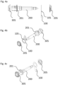
- the Fig. 3a to 3c show exploded views of the arrangement according to the Fig. 1a and 1b .
- the Fig. 4a to 4c show exploded views of the arrangement according to Fig. 12a and 2b .
- the individual components are pulled apart in the axial direction of the electrical pin-shaped contact element 200.
- the Fig. 5a and 5b each show a sectional view of an arrangement 300 with a temperature measuring device 100.
- the temperature measuring device 100 is shown schematically and can correspond to one of the embodiments described above or can also be modified. In particular, a sectional view along the longitudinal axis of the contact element 200 is shown.
- the arrangement 300 has a contact element 200, the temperature measuring device 100 and an elastic pressing element 205.
- the contact element 200 in particular of a charging socket, comprises an external plug-in area 302 for electrical contact with a charging gun.
- the contact element 200 comprises an output area 304 inside the vehicle, to which a high-voltage cable set is attached.
- first housing part 301 and a second housing part 303 are shown.
- the flange 201 of the pin-shaped electrical contact element 200 rests on the first housing part 301.
- the second housing part 303 exerts a force on the flexible circuit board 101 in the direction of the first housing part 301.
- the second housing part 303 rests on the temperature measuring device 100 by means of the elastic pressing element 205 and presses the temperature measuring device 100 with the support surface 113 against the flange 201.
- a further elastic pressing element 305 is arranged between the first housing part 301 and the support surface 113.
- the arrangement 300 comprises only one of the two elastic pressing elements 205, 305 or none and the first housing part 301 lies directly on the flange 201 or the second Housing part 303 lies directly on the flexible circuit board 101, in particular on the third insulating layer 117.
- Fig. 5a the contact element 200 is in a normal position. This means that no lateral force acts on the contact element 200, ie no force acts perpendicular to the main direction of extension of the pin-shaped contact element 200.
- no lateral force acts on the contact element 200, ie no force acts perpendicular to the main direction of extension of the pin-shaped contact element 200.
- canting or other impairments can occur which exert a lateral force on the contact element 200.
- a lateral force acts on the contact element 200, which is in a direction compared to the orientation according to Fig. 5a twisted alignment of the contact element 200, see arrows in Fig. 5a and 5b .
- the elastic pressing elements 205, 305 represent a flexible mounting of the contact element 200.
- the first housing part 301 and the second housing part 303 enclose the temperature measuring device 100, i.e. the measuring setup.
- Fig. 6 shows a flow chart 600 for a method for manufacturing a temperature measuring device 100 according to an embodiment.
- the first thermally conductive and electrically insulating substrate layer 101 is provided.
- the first substrate layer 101 has a support surface 113 which is designed to lie flat on a flange 201 of the pin-shaped electrical contact element 200.
- the support surface 113 has the opening 111, wherein the pin-shaped contact element 200 can be arranged at least partially in the opening 111.
- the second thermally and electrically conductive layer 103 is applied to the first substrate layer 101 provided.
- the second layer 103 has a sensor element 105 opposite the support surface 113, which is arranged on the sensor surface 107 of the first substrate layer 101.
- the sensor element 105 is applied to the first substrate layer 101 after the second layer 103 has been applied.
- the third insulating layer 117 is applied to the second layer 103.
- the third insulating layer 117 is glued to the first substrate layer 101 at the edge around the second layer 103.
- the third insulating layer 117 and the first substrate layer 101 are connected to one another in a different way.
- the third insulating layer 117 is omitted.
- An elastic pressing element 205 can lie directly on the second layer 103 and, in addition to pressing, also take over the electrical insulation.
- the temperature measuring device 100 is arranged on a pin-shaped electrical contact element 200.
- the temperature measuring device 100 can be plugged onto the contact element 200 or the contact element 200 can be inserted into the opening 111 of the temperature measuring device 100.
- the temperature measuring device 100 then rests with the support surface 113 on the flange 201 of the contact element 200, as described above in particular for the Fig. 1b , 2b , 5a and 5b described.
- step 605 the arrangement created in step 604 is arranged in a housing with the first housing part 301 and the second housing part 303.
- the elastic pressing element 205 and the further elastic pressing element 305 are placed between them.
- the interposition of one or both elastic pressing elements 205, 305 is omitted in step 605.
- Assembly can be automated. The following steps can be carried out here. Inserting the contact element 200 into the first housing part 301, possibly with another elastic pressure element 305 already inserted. Inserting an additional heat-conducting element, for example a graphite disk, onto the other elastic pressure element 305. This is followed by placing the first layer 101 onto the flange 201 of the contact element 200. A connection is made between the electrical line 109 of the second layer 103 and the evaluation unit or a plug or another contact system. The elastic pressure element, i.e. the seal, and the second housing part 303 can then be pushed on in order to press the temperature measuring device 100 onto the flange 201 of the contact element 200.
- one of the steps of inserting an additional heat conducting element or establishing a connection of the electrical Line 109 of the second layer 103 with the evaluation unit or both steps are omitted.
Landscapes
- Physics & Mathematics (AREA)
- Engineering & Computer Science (AREA)
- General Physics & Mathematics (AREA)
- Microelectronics & Electronic Packaging (AREA)
- Power Engineering (AREA)
- Transportation (AREA)
- Mechanical Engineering (AREA)
- Nonlinear Science (AREA)
- Measuring Temperature Or Quantity Of Heat (AREA)
Description
- Die vorliegende Erfindung betrifft eine Anordnung mit einer Temperaturmessvorrichtung.
- Steigende Stromstärken im Bereich der Elektromobilität bringen viele Leitungs- und Stecksysteme an ihre thermischen Grenzen. Ein solches Stecksystem kann beispielsweise eine Mehrzahl von stiftförmigen elektrischen Kontaktelementen, insbesondere Kontaktpins einer Ladedose eines Elektrofahrzeugs, aufweisen. Schon leicht erhöhte Übergangswiderstände an Schraub- oder Steckkontakten können zu kritischen Temperaturen führen, welche durch geeignete Überwachungsmaßnahmen rechtzeitig erkannt werden sollten.
- Infolge eines solchen Fehlerfalls kann beispielsweise die Ladeleistung oder die Antriebsleistung eines Elektrofahrzeugs reduziert werden, um die Überhitzung des Systems oder sogar einen Brand zu vermeiden.
- Hierfür kann eine Temperaturüberwachung eingerichtet werden, die ein solches Stecksystem thermisch überwacht. Hierfür kann eine Temperaturmessvorrichtung vorgesehen werden. Je genauer die Temperatur des Stecksystems gemessen werden kann, desto schneller kann auf eine kritische Temperatur reagiert werden.
- Eine Möglichkeit, die Temperatur an einem Kontaktelement zu messen ist eine Infrarotmessung. Andere Möglichkeiten umfassen beispielsweise wärmeleitende Elemente, die an der zylindrischen Fläche des Kontaktelements anliegen können.
- Die
DE 10 2018 120 057 A1 offenbart eine Temperaturmesseinrichtung für Steckverbinder, beinhaltend mindestens ein Trägerelement, mindestens ein Temperaturmessmittel samt Leiterbahnen sowie bedarfsweise mindestens ein aus Keramikmaterial bestehendes Deckelement, wobei das Temperaturmessmittel samt Leiterbahnen auf dem Trägerelement oder zwischen dem Trägerelement und dem bedarfsweisen Deckelement aufgebracht und zumindest mit einem der beiden Bauteile in Wirkverbindung steht, dergestalt, dass die Verbindung der Bauteile durch ein Glaslot erfolgt. - Die
CN 208 171 458 U und dieCN 208 238 969 U offenbaren jeweils ein Wärmeleitbauteil für einen Temperatursensor und einen Steckverbinder. - Die Aufgabe der Erfindung ist es, eine vorteilhafte Möglichkeit der Temperaturmessung aufzuzeigen.
- Die Aufgabe wird durch den Gegenstand des unabhängigen Anspruchs gelöst. Insbesondere wird die Aufgabe durch eine Anordnung mit einem stiftförmigen Kontaktelement und einer Temperaturmessvorrichtung zum Messen einer Temperatur des stiftförmigen Kontaktelements gemäß dem unabhängigen Anspruch gelöst. Vorteilhafte Weiterbildungen der Erfindung sind in der Beschreibung und den begleitenden Figuren angegeben.
- Die Temperaturmessvorrichtung umfasst eine flexible Leiterplatte mit einer ersten thermisch leitenden und elektrisch isolierenden Substratschicht mit einer Auflagefläche, die eingerichtet ist, an einem Flansch des stiftförmigen elektrischen Kontaktelements flächig aufzuliegen und einer in der Auflagefläche angeordneten Öffnung, wobei das stiftförmige Kontaktelement wenigstens teilweise in der Öffnung anordenbar ist; und einer zweiten thermisch und elektrisch leitenden Schicht, die auf einer der Auflagefläche gegenüberliegenden Sensorfläche der ersten Substratschicht angeordnet ist und ein mit der Sensorfläche verbundenes Sensorelement aufweist, das eingerichtet ist, eine Temperatur des stiftförmigen elektrischen Kontaktelements zu erfassen, wenn das stiftförmige elektrische Kontaktelement in der Öffnung wenigstens teilweise angeordnet ist.
- Hierdurch wird eine hochdynamische und trotzdem elektrisch isolierte Temperaturmessung an dem stiftförmigen elektrischen Kontaktelement, insbesondere zylindrischen stiftförmigen elektrischen Kontaktelement, ermöglicht. Das stiftförmige elektrische Kontaktelement kann gesteckt oder geschraubt an einer Ladedose angeordnet sein. Die Wärme des Kontaktelements kann vom Kontaktelement über den Flansch und durch die Auflagefläche und die erste Schicht zu der Sensorfläche und der zweiten Schicht fließen.
- Vorteile sind beispielsweise eine große Kontaktfläche zur Wärmeflussoptimierung, eine geringe thermische Masse zur Erhöhung der Messdynamik, eine gute elektrische Isolation, die bis in den höheren kV-Bereich skalierbar ist, eine hohe Robustheit gegenüber mechanischen Toleranzen und Schwingungen, sowie ein einfaches und automatisierbares Montagekonzept, um die Skalierbarkeit bei hohen Stückzahlen zu gewährleisten. Ein Abwägen von Messgenauigkeit und automatisierter Montierbarkeit gegeneinander kann so vermieden werden.
- Die Temperaturmessvorrichtung stellt demnach einen Flachleiter mit einem Temperaturmesselement dar, die auf einem Flansch, d.h. einem Absatz, des stiftförmigen elektrischen Kontaktelements angeordnet sein kann. Insbesondere kann das stiftförmige elektrische Kontaktelement ein Leistungskontakt eines Ladesystems für (hybrid)elektrische Fahrzeuge (Ladedose bzw. Ladepistole) sein und mit der Temperaturmessvorrichtung kann die Temperatur des Leistungskontakts überwacht werden.
- Das stiftförmige elektrische Kontaktelement weist den Flansch auf, durch welchen eine ebene Messfläche entsteht, auf welche die flexible Leiterplatte mit der Auflagefläche durch, insbesondere ein elastisches Anpresselement, andrückbar ist. Der Flansch kann speziell für diesen Zweck ausgeprägt sein, z.B. als umlaufender Tellerbereich eines zylindrischen Steckkontakts. Der Flansch kann ebenso eine anderweitig ausgeprägte ebene Fläche, welche insbesondere orthogonal zur Längsachse des zylindrischen Kontaktelements, d.h. des stiftförmigen elektrischen Kontaktelements, liegt, als Auflage- und Messfläche des Flachleiters genutzt werden. Hierfür kann beispielsweise ein angeschweißter Kabelschuh oder ein angeschraubter Kabelschuh oder eine angeschweißte Stromschiene oder eine angeschraubte Stromschiene in Frage kommen. Der Flansch ist insbesondere orthogonal gegenüber der Längsachse des stiftförmigen elektrischen Kontaktelements angeordnet und schafft so eine ausgerichtete Messfläche zur Messung der Temperatur. Hierdurch kann ein automatisierter Sandwichaufbau ermöglicht werden.
- Die Temperaturmessvorrichtung ermöglicht eine elektrisch isolierte und thermisch hochdynamische Sensoranbindungen, und kann einen raschen Temperaturanstieg schnell und zuverlässig erkennen. Die Temperaturmessvorrichtung ist eine kostengünstige und automatisierbare Lösung und kann so den steigenden Stückzahlen im Bereich der Elektromobilität Rechnung tragen. Insbesondere kann zwischen stiftförmigen elektrischen Kontaktelement und der zweiten Schicht, welche insbesondere durch Laminieren oder Kleben auf die erste Schicht aufgebracht wird, die elektrische Isolation der innenliegenden Sensorfläche und Leiterbahnen gewährleistet sein.
- Die flexible Leiterplatte kann ein Flachleiter, d.h. eine Flexplatine sein. Die flexible Leiterplatte kann ein flexibles, elektrisch isolierendes Substrat als erste Schicht aufweisen, welches eine Potentialtrennung zwischen dem stiftförmigen elektrischen Kontaktelement und dem Sensorelement bereitstellen kann. Das stiftförmige elektrische Kontaktelement kann beispielsweise einem elektrischen Potential zwischen ca. 400 V und 1000 V zugeordnet sein. Das Sensorelement kann insbesondere einem niedrigeren Potential, z.B. dem Niedervoltbordnetz eines Fahrzeugs, zugeordnet sein.
- Die erste Substratschicht weist eine Öffnung auf, durch welche das stiftförmige elektrische Kontaktelement führbar ist. Insbesondere ist die Öffnung ein Loch und das stiftförmige elektrische Kontaktelement kann durch die Öffnung gesteckt werden. Dabei weist die erste Substratschicht eine Auflagefläche und eine der Auflagefläche gegenüberliegende Sensorfläche auf.
- Die Auflagefläche ist thermisch an das stiftförmige elektrische Kontaktelement anbindbar, d.h. die erste Substratschicht kann mit der Auflagefläche direkt auf dem stiftförmigen elektrischen Kontaktelement aufliegen. Auch kann zwischen dem stiftförmigen elektrischen Kontaktelement und der Auflagefläche eine wärmeleitende Schicht eingebracht sein, durch die die Auflagefläche an das stiftförmige elektrische Kontaktelement angebunden ist. Die Sensorfläche des Flachleiters kann so ausgeprägt sein, dass sie die Auflagefläche auf dem Absatz des Kontaktelements widerspiegelt und somit eine maximale Wärmedurchflussfläche nutzt.
- Die wärmeleitende Schicht kann beispielsweise Grafit oder einen metallischen Werkstoff umfassen und dient der Wärmespreizung, um die Wärmedurchflussfläche zu vergrößern. Die wärmeleitende Schicht kann sehr dünn ausgeführt sein, insbesondere dünner als 1 mm, um die zusätzliche thermische Masse im Messpfad zu minimieren. Die wärmeleitende Schicht kann dabei mit der ersten Substratschicht, d.h. dem flexiblen Substrat, verbunden sein, insbesondere an der Auflagefläche auflaminiert oder aufgeklebt sein, oder fest an dem stiftförmigen elektrischen Kontaktelement angebracht sein, beispielsweise geklebt, gelötet oder geschweißt sein, oder eine eigenständige Komponente sein, insbesondere eine auflegbare Scheibe.
- In einer Ausgestaltung ist die Auflagefläche geometrisch an den Flansch des stiftförmigen elektrischen Kontaktelements angepasst.
- Hierbei kann die Auflagefläche so gestaltet sein, dass eine möglichst große Fläche auf dem Flansch des stiftförmigen elektrischen Kontaktelements aufliegt. Darüber hinaus kann die Geometrie der flexiblen Leiterplatte so gestaltet sein, dass diese leichte Bewegungen des stiftförmigen elektrischen Kontaktelements, beispielsweise verursacht durch die Montage, geometrische Toleranzen oder Erschütterungen, ausgleichen kann, ohne dabei die zweite thermisch und elektrisch leitende Schicht, die Sensorfläche oder den ggfs. aufgelöteten SMD-Sensor zu beschädigen.
- In einer Ausgestaltung umfasst das Sensorelement eine flächige Leiterbahn, die auf der Sensorfläche angeordnet ist und einen Sensor, d.h. insbesondere einen Temperaturfühler, umfasst, der thermisch mit der flächigen Leiterbahn verbunden ist.
- Dadurch wird der Temperaturfühler, d.h. der Temperatursensor sehr nah an das stiftförmige elektrische Kontaktelement gebracht, sodass ein geringer Verlust bei der Wärmeübertragung zu dem Temperaturfühler hin gewährleistet werden kann. Hierbei umfasst die Sensorfläche den Temperaturfühler selbst. Die Sensorfläche kann hierbei als Erweiterung einer Leitbahn ausgeführt sein, welche die Wärme in den aufgelöteten Temperatursensor leitet.
- In einer Ausgestaltung weist die Sensorfläche ein Material mit einem temperaturabhängigen Widerstand auf.
- Die Sensorfläche kann mit einem Material versehen werden, welches einen temperaturabhängigen elektrischen Widerstand aufweist, insbesondere einen möglichst starken temperaturabhängigen elektrischen Widerstand. Hierfür eignen sich insbesondere Platin oder Nickel. Beispielsweise kann ein Platindraht auf die Sensorfläche auf die erste Substratschicht auflaminiert oder aufgeklebt werden. Das Material, das den temperaturabhängigen elektrischen Widerstand aufweist kann das Sensorelement darstellen. Das Sensorelement kann außerhalb der Sensorfläche mit einer elektrischen Leitung verbunden sein. Hierbei kann mit einer dritten elektrisch isolierenden Schicht eine vollständige elektrische Isolation der Temperaturmessvorrichtung erfolgen, da das Sensorelement nicht durch die Isolation hindurchragt. Der Aufbau wird auch flacher.
- In einer Ausgestaltung umfasst die Sensorfläche einen mäanderförmig angeordneten Metalldraht. Hierbei kann die Sensorfläche weitmöglichst ausgenutzt werden.
- In einer Ausgestaltung ist der mäanderförmig angeordnete Metalldraht in einem niederinduktiven Layout angeordnet.
- Hierdurch kann eine Einkopplung elektromagnetischer Felder durch den im stiftförmigen elektrischen Kontaktelement fließenden Strom in die Sensorbahn verringert, insbesondere minimiert, werden.
- In einer Ausgestaltung umfasst die Sensorfläche eine strukturierte Metallfolie. Die strukturierte Metallfolie kann insbesondere eine Platin- oder Nickelfolie sein, welche beispielsweise über Laser- oder Ätzprozesse strukturiert wird. Die Struktur kann hierbei den gleichen Maßstäben genügen, wie zu dem mäanderförmigen Metalldraht beschrieben.
- In einer Ausgestaltung umfasst die Temperaturmessvorrichtung eine dritte isolierende Schicht auf der zweiten Schicht.
- Hierbei kann eine Kriechstrecke des elektrischen Stroms von dem stiftförmigen elektrischen Kontaktelement, d.h. dem Hochvoltbereich, hin zu dem Sensorelement, d.h. dem Niedervoltbereich, erhöht werden. Das hießt, es kann Luft- und/oder Kriechstrecken für die elektrische Isolation der Potentiale des Sensorelements und/oder des stiftförmigen elektrischen Kontaktelements Rechnung getragen werden. Somit kann eine zusätzliche Isolationsschicht auf der Sensorfläche vorgesehen sein. Diese kann beispielsweise durch Kleben oder Laminieren einer dritten flexiblen isolierenden Substratschicht realisiert werden.
- Die strukturierte Metallfolie kann mit einem Sensor, insbesondere einem SMD-Sensor, verbunden sein. Hierbei kann die dritte Substratschicht an der Position des Sensors eine Öffnung aufweisen, durch welche der Sensor im Fertigungsprozess aufgelötet werden kann. Um die elektrische Isolation auch an diesem Bauteil zu realisieren, kann der Sensor mit einer Glob Top Vergussmasse bedeckt werden. So kann der Sensor elektrisch isoliert werden.
- Wenn die Sensorfläche direkt als Platin- oder Nickelbahn ausgeführt ist, d.h. insbesondere als mäanderförmig angeordneter Metalldraht, kann die bedeckende dritte Substratschicht ohne weitere Öffnungen aufgebracht werden um die gesamte Sensorfläche und ggf. auch angrenzende Bereiche der flexiblen Leiterplatte elektrisch zu isolieren. Die Öffnung, in der das stiftförmige Kontaktelement wenigstens teilweise anordenbar ist, ist in jeder der Substratschichten ausgebildet.
- In einer Ausgestaltung umfasst die zweite Schicht wenigstens eine elektrische Leitung, die eingerichtet ist, die Temperaturmessvorrichtung elektronisch mit einer Auswerteeinheit zu verbinden. Die elektrische Leitung kann eine Möglichkeit zur elektrischen Kontaktierung und eine Signalleitung bereitstellen.
- Hierbei wird weitere Peripherie in die flexible Leiterplatte eingebunden und zusätzliche Kabel oder Leitungen, die Platz benötigen, können vermieden werden. Von der Sensorfläche bzw. dem Sensor, insbesondere dem SMD-Sensor, führen Leiterbahnen weg zu einer Auswerteeinheit, welche entweder auf dem flexiblen Substrat mit aufgebracht sein kann oder aber durch eine Steck-, Löt-, Schweiß- oder Crimpverbindung mit den Leiterbahnen elektrisch direkt oder indirekt, beispielsweise über ein weiteres Kabel, verbunden ist.
- Erfindungsgemäß wird die Aufgabe durch eine Anordnung mit einem stiftförmigen Kontaktelement und einer Temperaturmessvorrichtung zum Messen einer Temperatur des stiftförmigen Kontaktelements gemäß dem unabhängigen Anspruch gelöst.
- Die Anordnung umfasst ein Gehäuse mit einem ersten Gehäuseteil und einem zweiten Gehäuseteil, wobei der Flansch des stiftförmigen elektrischen Kontaktelements an dem ersten Gehäuseteil anliegt und wobei das zweite Gehäuseteil eine Kraft auf die flexible Leiterplatte in Richtung der ersten Gehäuseteils ausübt und die Auflagefläche der flexiblen Leiterplatte so gegen den Flansch des stiftförmigen elektrischen Kontaktelements drückt. Hierbei kann die Temperaturmessvorrichtung sicher fixiert werden.
- Zwischen der flexiblen Leiterplatte und dem zweiten Gehäuseteil ist ein elastisches Anpresselement angeordnet. Hierbei wird der Druck über das elastische Anpresselement auf die flexible Leiterplatte ausgeübt.
- Das elastische Anpresselement, beispielsweise eine Dichtung wie ein O-Ring, kann dazu dienen, die flexible Leiterplatte auf den Flansch des Kontaktelements zu drücken. Die elastische Eigenschaft kann dazu dienen, dass auch bei thermischer Ausdehnung des stiftförmigen elektrischen Kontaktelements oder einem mechanischen Spiel in einer Verankerung des stiftförmigen elektrischen Kontaktelements immer ein ausreichender Anpressdruck auf die flexible Leiterplatte herrscht. Dadurch soll die flexible Leiterplatte mit ihrem Kontaktbereich, d.h. der Auflagefläche, möglichst großflächig und ohne Luftspalt auf dem stiftförmigen elektrischen Kontaktelement aufliegen um den Wärmefluss vom stiftförmigen elektrischen Kontaktelement zu der Sensorfläche der flexiblen Leiterplatte unter allen Umgebungsbedingungen zu gewährleisten, insbesondere zu verbessern, weiter insbesondere zu maximieren. Im Anwendungsfall einer Ladedose kann das elastische Anpresselement durch eine Dichtung des stiftförmigen elektrischen Kontaktelements realisiert sein. Hierfür wird die Dichtung so weit entlang des stiftförmigen elektrischen Kontaktelements verlängert, dass sie im fertig montierten Zustand durch einen leichten Überstand gegenüber dem Flansch des Kontaktelements den dazwischenliegenden Flachleiter auf den Flansch des Kontaktelements presst.
- Zwischen dem Flansch des stiftförmigen elektrischen Kontaktelements und dem ersten Gehäuseteil ist ein weiteres elastisches Anpresselement angeordnet. Dies kann eine weitere Flexibilität bringen und trotzdem einen sicheren anpressdruck der Temperaturmessvorrichtung auf den Flansch gewährleisten.
- Nicht erfindungsgemäß ist ein Verfahren zum Herstellen einer Temperaturmessvorrichtung zum Messen einer Temperatur eines stiftförmigen elektrischen Kontaktelements, umfassend ein Bereitstellen einer ersten thermisch leitenden und elektrisch isolierenden Substratschicht einer flexiblen Leiterplatte mit einer Auflagefläche, die eingerichtet ist, an einem Flansch des stiftförmigen elektrischen Kontaktelements flächig aufzuliegen und einer in der Auflagefläche angeordneten Öffnung, wobei das stiftförmige Kontaktelement wenigstens teilweise in der Öffnung anordenbar ist; und ein Aufbringen einer zweiten thermisch und elektrisch leitenden Schicht auf die bereitgestellte erste Substratschicht, aufweisend ein auf einer der Auflagefläche gegenüberliegenden Sensorfläche der ersten Substratschicht angeordnetes Sensorelement, das eingerichtet ist, eine Temperatur des stiftförmigen elektrischen Kontaktelements an der Auflagefläche zu erfassen, wenn das stiftförmigen elektrischen Kontaktelements in der Öffnung wenigstens teilweise angeordnet ist.
- In einer Ausgestaltung umfasst das Verfahren ein Aufbringen einer dritten isolierenden Schicht auf die zweiten Schicht.
- Nachfolgend wird die Erfindung anhand von Ausführungsbeispielen und Figuren erläutert. Es zeigen:
- Fig. 1a
- eine nicht erfindungsgemäße Temperaturmessvorrichtung gemäß einem Ausführungsbeispiel,
- Fig. 1b
- eine Anordnung mit der Temperaturmessvorrichtung gemäß dem Ausführungsbeispiel von
Fig. 1a , - Fig. 2a
- eine nicht erfindungsgemäße Temperaturmessvorrichtung gemäß einem weiteren Ausführungsbeispiel,
- Fig. 2b
- eine Anordnung mit der Temperaturmessvorrichtung gemäß dem Ausführungsbeispiel von
Fig. 2a - Fig. 3a
- eine perspektivische Explosionsdarstellung der Anordnung aus
Fig. 1b , - Fig. 3b
- eine weitere perspektivische Explosionsdarstellung der Anordnung aus
Fig. 1b , - Fig. 3c
- eine weitere perspektivische Explosionsdarstellung der Anordnung aus
Fig. 1b , - Fig. 4a
- eine perspektivische Explosionsdarstellung der Anordnung aus
Fig. 2b , - Fig. 4b
- eine weitere perspektivische Explosionsdarstellung der Anordnung aus
Fig. 2b , - Fig. 4c
- eine weitere perspektivische Explosionsdarstellung der Anordnung aus
Fig. 2b , - Fig. 5a
- eine Anordnung mit einer Temperaturmessvorrichtung gemäß einem Ausführungsbeispiel in einer ersten Lage,
- Fig. 5b
- die Anordnung gemäß
Fig. 5a in einer zweiten Lage, und - Fig. 6
- ein Flussdiagramm für ein nicht erfindungsgemäßes Verfahren gemäß einem Ausführungsbeispiel.
- Die Figuren sind lediglich schematische Darstellungen und dienen der Erläuterung der Erfindung. Gleiche oder gleichwirkende Elemente sind mit den gleichen Bezugszeichen versehen. Zum leichteren Verständnis werden in der folgenden Beschreibung die Bezugszeichen zu den Figuren als Referenz beibehalten.
-
Fig. 1a zeigt eine Temperaturmessvorrichtung 100 gemäß einem Ausführungsbeispiel. Die Temperaturmessvorrichtung 100 weist eine erste thermisch leitende und elektrisch isolierende Substratschicht 101 auf. Die erste Substratschicht 101 ist eine außenliegende Schicht einer flexiblen Leiterplatte. - Auf der ersten Substratschicht 101 ist eine zweite thermisch und elektrisch leitende Schicht 103 aufgebracht. Die zweite Schicht 103 umfasst ein Sensorelement 105. Das Sensorelement 105 ist als Leiterbahn ausgestaltet, insbesondere aus Platin- oder Nickel. Hierbei ist das Sensorelement 105 als Metalldraht ausgeführt, der mäanderartig auf einer Sensorfläche 107 aufgebracht ist, in
Fig. 1 aus Gründen der Übersichtlichkeit jedoch lediglich als Fläche dargestellt. In einem weiteren Ausführungsbeispiel ist das Sensorelement 105 eine Folie. Das Sensorelement 105 weist ein Material mit einem temperaturabhängigen Widerstand auf. - Auf der ersten Substratschicht 101 ist des Weiteren eine elektrische Leitung 109 angeordnet, insbesondere umfasst die elektrische Leitung 109 zwei Leiterbahnen. Die elektrische Leitung 109 bildet eine elektrische Kontaktierung des Sensorelements 105 und dient als Signalleitung. Über die elektrische Leitung 109 wird der Widerstand des Sensorelements 105 von einer Auswerteeinheit, die in den Figuren aus Gründen der Übersichtlichkeit nicht dargestellt ist, gemessen.
- Die Temperaturmessvorrichtung 100 weist eine Öffnung 111 auf. Die Öffnung 111 ist hierbei ein Loch. In einem weiteren Ausführungsbeispiel kann die Öffnung 111 so angeordnet sein, dass die Sensorfläche 107 u-förmig ist. Das heißt, die Öffnung 111 kann eine Einkerbung in der Temperaturmessvorrichtung 100 sein.
-
Fig. 1b zeigt eine Anordnung der Temperaturmessvorrichtung 100 gemäß dem Ausführungsbeispiel ausFig. 1a und einem stiftförmigen elektrischen Kontaktelement 200. InFig. 1b ist lediglich ein Ausschnitt des Kontaktelements 200 dargestellt, insbesondere erstreckt sich das Kontaktelement 200 senkrecht zu der Temperaturmessvorrichtung 100 weiter als in derFig. 1b dargestellt. Das Kontaktelement 200 weist einen Flansch 201 auf. - Die Temperaturmessvorrichtung 100 weist eine Auflagefläche 113 auf. Die Temperaturmessvorrichtung 100 liegt mit der Auflagefläche 113 flächig auf dem Flansch 201 auf. Hierdurch ergibt sich eine große Kontaktfläche zwischen dem Kontaktelement 200 und der Temperaturmessvorrichtung 100, über die Wärme von dem Kontaktelement 200 zu der Temperaturmessvorrichtung 100 geführt werden kann, d.h. über die Wärme von dem Kontaktelement 200 das Sensorelement 105 der Temperaturmessvorrichtung 100 erwärmen kann. Da die erste Substratschicht 101 dünn ist, ist hierbei der Wärmeverlust gering.
- Die Öffnung 111 der Temperaturmessvorrichtung 100 ist an eine Außenkontur des stiftförmigen elektrischen Kontaktelements 200 angepasst, sodass zwar ein Spalt 203 zwischen Kontaktelement 200 und Temperaturmessvorrichtung 100 zum Ausgleich von Toleranzen und Bewegungen entsteht, der Spalt 203 jedoch gleichzeitig so klein bleibt, dass die Oberfläche des Flansches 201 von der Auflagefläche 113 zu einem möglichst großen Teil bedeckt werden kann.
- In
Fig. 1b ist zwischen dem Sensorelement 105 und der elektrischen Leitung 109 ein Übergang 115 zu sehen, an dem das Sensorelement 105 und die elektrische Leitung 109 miteinander verbunden sind. Hierbei sind die beiden unterschiedlichen Materialien miteinander verlötet. In einem weiteren Ausführungsbeispiel handelt es sich um die gleichen Materialien und/oder es wird eine andere Art der Verbindung gewählt als Löten. - In
Fig. 1b ist des Weiteren eine dritte isolierende Schicht 117 dargestellt. Die dritte isolierende Schicht 117 ist auf der zweiten Schicht 103 aufgebracht. Die dritte isolierende Schicht 117 schützt die zweite Schicht 103 vor Umwelteinflüssen und stellt eine elektrische Isolierung sowohl des Sensorelements 105, als auch der elektrischen Leitung 109 dar. In einem weiteren Ausführungsbeispiel kann diese dritte Schicht entfallen und die elektrische Isolierung kann durch ein elastisches Anpresselement 205, d.h. ein aufpressbares Element, erfolgen, beispielsweise eine Dichtung. Die zweite Schicht 103 wird an der Auflagefläche 113 von der dritten isolierenden Schicht 117 vollständig bedeckt. In einem weiteren Ausführungsbeispiel bedeckt die dritte isolierende Schicht 117 die zweite Schicht 103 lediglich teilweise. - Die Sensorfläche 107 ist so groß gewählt, das ein Rand an der ersten Substratschicht 101 über die zweite Schicht 103 übersteht, sodass eine Verklebung der ersten Substratschicht 101 mit der dritte isolierende Schicht 117 möglich ist, um die elektrische Isolierung der zweiten Schicht 103 zu gewährleisten. Insbesondere beträgt der Rand wenigstens 100µm für das Verkleben. Ein Rand von 1 mm bis 2 mm kann nach dem Verkleben der ersten Substratschicht 101 mit der dritten isolierenden Schicht 117 eine größere horizontale Isolation bzw. eine größere Kriechstrecke bieten. In einem weiteren Ausführungsbeispiel wird statt einem Verkleben ein Verschweißen der ersten Substratschicht 101 mit der dritten isolierenden Schicht 117 verwendet. Die Verbindung der ersten Substratschicht 101 mit der dritten isolierenden Schicht 117 kann insbesondere 130 Grad Celsius aushalten, um ein Lösen im Betrieb zu vermeiden.
- In
Fig. 1b ist ein elastisches Anpresselement 205 dargestellt, das zusätzlich zu der dritten isolierenden Schicht 117 verwendet wird. Das elastische Anpresselement 205 ist ein elastisches Element, beispielsweise eine Dichtung, das auf die Temperaturmessvorrichtung 100 pressbar ist, um die Temperaturmessvorrichtung 100 in Position zu halten. Dies wird zu denFig. 5a und 5b genauer beschrieben. - In
Fig. 2a ist eine Temperaturmessvorrichtung 100 gemäß einem weiteren Ausführungsbeispiel dargestellt. Wie zu dem Ausführungsbeispiel vonFig. 1a beschrieben, weist die Temperaturmessvorrichtung 100 gemäßFig. 2a eine erste Substratschicht 101, eine Sensorfläche 107, und eine zweite Schicht 103 auf. Das Sensorelement 105 ist jedoch als SMD-Temperaturfühler, insbesondere als PT1000 oder NTC, ausgeführt. Die Sensorfläche 105 ist hierbei als Leitbahn ausgeführt, welche die Wärme in das Sensorelement 105, d.h. hier den aufgelöteten Temperatursensor, leitet. Wie zuFig. 1a beschrieben kann das Sensorelement 105 über die elektrische Leitung 109 ausgelesen werden. Die Öffnung 111 ist gleichermaßen wie zuFig. 1a beschrieben ausgestaltet. -
Fig. 2b zeigt eine Anordnung, wie zuFig. 1b beschrieben, wobei jedoch als Temperaturmessvorrichtung 100 die Temperaturmessvorrichtung 100 gemäß dem Ausführungsbeispiel vonFig. 2a verwendet wird, bei der das Sensorelement 105 einen SMD-Temperaturfühler umfasst. - Das Sensorelement 105 der Temperaturmessvorrichtung 100 gemäß dem Ausführungsbeispiel zu den
Fig. 2a und 2b weist in der dritten isolierenden Schicht 117 im Bereich des Sensorelements 105 eine Unterbrechung auf, sodass das Sensorelement 105 direkt auf der zweiten Schicht 103 angeordnet, insbesondere aufgelötet, sein kann. Die Unterbrechung in der dritten isolierenden Schicht 117 und das Sensorelement 105 sind hierbei mit einer Vergussmasse 119, insbesondere einer Glob Top Vergussmasse, bedeckt und so elektrisch isoliert und gegen Umwelteinflüsse geschützt. - In die Öffnung 111 ist in allen Ausführungsbeispielen ein stiftförmiges elektrisches Kontaktelement anordenbar, dessen Temperatur gemessen werden soll.
- Die
Fig. 3a bis 3c zeigen Explosionsdarstellungen der Anordnung gemäß denFig. 1a und 1b . DieFig. 4a bis 4c zeigen Explosionsdarstellungen der Anordnung gemäß den Fig. 12a und2b . Hierbei sind die einzelnen Komponenten in axialer Richtung des elektrischen stiftförmigen Kontaktelements 200 auseinandergezogen. - Die
Fig. 5a und 5b zeigen jeweils eine Schnittdarstellung einer Anordnung 300 mit einer Temperaturmessvorrichtung 100. Die Temperaturmessvorrichtung 100 ist schematisch dargestellt und kann einem der oben beschriebenen Ausführungsbeispiele entsprechen oder auch abgewandelt sein. Insbesondere wird eine Schnittansicht entlang der Längsachse des Kontaktelements 200 dargestellt. - Wie zu den
Fig. 1b und2b oben beschrieben weist die Anordnung 300 ein Kontaktelement 200, die Temperaturmessvorrichtung 100 und ein elastisches Anpresselement 205 auf. Das Kontaktelement 200, insbesondere einer Ladedose, umfasst einen äußeren Steckbereich 302 zur elektrischen Kontaktierung mit einer Ladepistole. Das Kontaktelement 200 umfasst einen fahrzeuginneren Abgangsbereich 304, an welcher ein Hochvoltkabelsatz angehängt ist. - Zusätzlich sind ein erstes Gehäuseteil 301 und zweites Gehäuseteil 303 dargestellt. Der Flansch 201 des stiftförmigen elektrischen Kontaktelements 200 liegt an dem ersten Gehäuseteil 301 an. Das zweite Gehäuseteil 303 übt eine Kraft auf die flexible Leiterplatte 101 in Richtung des ersten Gehäuseteils 301 aus. Das zweite Gehäuseteil 303 liegt hierbei mittels dem elastisches Anpresselement 205 auf der Temperaturmessvorrichtung 100 an und drückt die Temperaturmessvorrichtung 100 mit der Auflagefläche 113 gegen den Flansch 201.
- Zwischen dem ersten Gehäuseteil 301 und der Auflagefläche 113 ist ein weiteres elastisches Anpresselement 305 angeordnet. In einem weiteren Ausführungsbeispiel umfasst die Anordnung 300 lediglich eines der beiden elastischen Anpresselemente 205, 305 oder keines und das erste Gehäuseteil 301 liegt direkt an dem Flansch 201 an bzw. das zweite Gehäuseteil 303 liegt direkt an der flexiblen Leiterplatte 101 an, insbesondere auf der dritten isolierenden Schicht 117.
- In
Fig. 5a ist das Kontaktelement 200 in einer normalen Position. Das heißt, es wirkt keine seitliche Kraft auf das Kontaktelement 200, d.h. es wirkt keine Kraft senkrecht zur Haupterstreckungsrichtung des stiftförmigen Kontaktelements 200. Beispielsweise bei einem Aufstecken eines Ladesteckers, in den Fig. nicht dargestellt, kann es jedoch zu Verkantungen oder anderen Beeinträchtigungen kommen, die eine seitliche Kraft auf das Kontaktelement 200 ausüben. - Ein solcher Fall ist schematisch in
Fig. 5b dargestellt. Hierbei wirkt auf das Kontaktelement 200 eine seitliche Kraft, die in einer im Vergleich zur Ausrichtung gemäßFig. 5a verdrehten Ausrichtung des Kontaktelements 200 resultiert, siehe Pfeile inFig. 5a und 5b . - Die elastischen Anpresselemente 205, 305 stellen hierbei eine flexible Lagerung des Kontaktelements 200 dar. Das erste Gehäuseteil 301 und das zweite Gehäuseteil 303 fassen die Temperaturmessvorrichtung 100, d.h. den Messaufbau, ein.
-
Fig. 6 zeigt ein Flussdiagramm 600 für ein Verfahren zum Herstellen einer Temperaturmessvorrichtung 100 gemäß einem Ausführungsbeispiel. - In einem Schritt 601 wird die erste thermisch leitende und elektrisch isolierende Substratschicht 101 bereitgestellt. Die erste Substratschicht 101 weist eine Auflagefläche 113 auf, die eingerichtet ist, an einem Flansch 201 des stiftförmigen elektrischen Kontaktelements 200 flächig aufzuliegen. Die Auflagefläche 113 weist die Öffnung 111 auf, wobei das stiftförmige Kontaktelement 200 wenigstens teilweise in der Öffnung 111 anordenbar ist.
- In einem folgenden Schritt 602 wird die zweite thermisch und elektrisch leitende Schicht 103 auf die bereitgestellte erste Substratschicht 101 aufgebracht. Die zweite Schicht 103 weist ein auf der der Auflagefläche 113 gegenüberliegendes Sensorelement 105 auf, das auf der Sensorfläche 107 der ersten Substratschicht 101 angeordnet ist. In einem weiteren Ausführungsbeispiel wird das Sensorelement 105 nach dem Aufbringen der zweiten Schicht 103 auf die erste Substratschicht 101 aufgebracht.
- In einem Schritt 603 wird die dritte isolierenden Schicht 117 auf die zweiten Schicht 103 aufgebracht. Hierbei wird die dritte isolierende Schicht 117 mit der ersten Substratschicht 101 an dem Rand um die zweite Schicht 103 herum verklebt. In einem weiteren Ausführungsbeispiel werden die dritte isolierende Schicht 117 und die erste Substratschicht 101 anders miteinander verbunden. In einem alternativen Ausführungsbeispiel wird auf die dritte isolierende Schicht 117 verzichtet. Hierbei kann ein elastisches Anpresselement 205 direkt auf der zweiten Schicht 103 aufliegen und neben einem Anpressen auch die elektrische Isolierung mitübernehmen.
- In einem Schritt 604 wird die Temperaturmessvorrichtung 100 auf einem stiftförmigen elektrischen Kontaktelement 200 angeordnet. Hierbei kann die Temperaturmessvorrichtung 100 auf das Kontaktelement 200 aufgesteckt oder aber auch das Kontaktelement 200 in die Öffnung 111 der Temperaturmessvorrichtung 100 eingeführt werden. Hierbei liegt dann die Temperaturmessvorrichtung 100 mit der Auflagefläche 113 auf dem Flansch 201 des Kontaktelements 200 an, wie oben insbesondere zu den
Fig. 1b ,2b ,5a und 5b beschrieben. - In einem Schritt 605 werden wird die in Schritt 604 erstellte Anordnung in ein Gehäuse mit dem ersten Gehäuseteil 301 und dem zweiten Gehäuseteil 303 angeordnet. Hierbei werden das elastische Anpresselement 205 und das weiteres elastische Anpresselement 305 zwischengelegt. In einem weiteren Ausführungsbespiel entfällt im Schritt 605 das Zwischenlegen eines oder beider elastischen Anpresselemente 205, 305.
- Eine Montage kann automatisiert erfolgen. Hierbei können folgende Schritte durchgeführt werden. Einführen des Kontaktelements 200 in den ersten Gehäuseteil 301, gegebenenfalls mit bereits eingelegtem weiteren elastischen Anpresselement 305. Einlegen eines zusätzlichen Wärmeleitelements, beispielsweise einer Grafitscheibe auf das weitere elastische Anpresselement 305. Es folgt ein Auflegen der ersten Schicht 101 auf den Flansch 201 des Kontaktelements 200. Es wird eine Verbindung der elektrischen Leitung 109 der zweiten Schicht 103 mit der Auswerteeinheit oder einem Stecker oder einem anderen Kontaktsystem hergestellt. Dann kann ein Aufschieben des elastischen Anpresselements, d.h. der Dichtung, und des zweiten Gehäuseteils 303 erfolgen, um die Temperaturmessvorrichtung 100 auf den Flansch 201 des Kontaktelements 200 zu drücken.
- In einem weiteren Ausführungsbeispiel kann einer der Schritte des Einlegens eines zusätzlichen Wärmeleitelements oder des Herstellens einer Verbindung der elektrischen Leitung 109 der zweiten Schicht 103 mit der Auswerteeinheit oder auch beide Schritte entfallen.
-
- 100
- Temperaturmessvorrichtung
- 101
- erste Substratschicht
- 103
- zweite Schicht
- 105
- Sensorelement
- 107
- Sensorfläche
- 109
- elektrische Leitung
- 111
- Öffnung
- 113
- Auflagefläche
- 115
- Übergang
- 117
- dritte isolierende Schicht
- 119
- Vergussmasse
- 200
- Kontaktelement
- 201
- Flansch
- 203
- Spalt
- 205
- elastisches Anpresselement
- 300
- Anordnung
- 301
- erstes Gehäuseteil
- 302
- äußerer Steckbereich
- 303
- zweites Gehäuseteil
- 304
- fahrzeuginnerer Abgangsbereich
- 305
- weiteres elastisches Anpresselement
- 600
- Flussdiagramm
- 601 -605
- Verfahrensschritt
Claims (1)
- Anordnung (300) mit einem stiftförmigen Kontaktelement (200) und einer Temperaturmessvorrichtung (100) zum Messen einer Temperatur des stiftförmigen elektrischen Kontaktelements (200), die Temperaturmesseinrichtung (100) umfassend eine flexible Leiterplatte mit einer ersten thermisch leitenden und elektrisch isolierenden Substratschicht (101) mit einer Auflagefläche (113), die eingerichtet ist, an einem Flansch (201) des stiftförmigen elektrischen Kontaktelements (200) flächig aufzuliegen und einer in der Auflagefläche (113) angeordneten Öffnung (111), wobei das stiftförmige Kontaktelement (200) wenigstens teilweise in der Öffnung (111) angeordnet ist; undeiner zweiten thermisch und elektrisch leitenden Schicht (103), die auf einer der Auflagefläche (113) gegenüberliegenden Sensorfläche (107) der ersten Substratschicht (101) angeordnet ist und ein mit der Sensorfläche (107) verbundenes Sensorelement (105) aufweist, das eingerichtet ist, eine Temperatur des stiftförmigen elektrischen Kontaktelements (200) zu erfassen, wobeidie Auflagefläche (113) der flexiblen Leiterplatte flächig an dem Flansch (201) des stiftförmigen elektrischen Kontaktelements (200) aufliegt,dadurch gekennzeichnet, dass die Anordnung (300) ein Gehäuse mit einem ersten Gehäuseteil (301) und einem zweiten Gehäuseteil (303) umfasst,wobei der Flansch (201) des stiftförmigen elektrischen Kontaktelements (200) an dem ersten Gehäuseteil (301) anliegt und wobei das zweite Gehäuseteil (303) eine Kraft auf die flexible Leiterplatte in Richtung des ersten Gehäuseteils (301) ausübt und die Auflagefläche (113) der flexiblen Leiterplatte so gegen den Flansch (201) des stiftförmigen elektrischen Kontaktelements (200) drückt, wobei zwischen der flexiblen Leiterplatte und dem zweiten Gehäuseteil (303) ein elastisches Anpresselement (205) angeordnet ist und wobei der Druck über das elastische Anpresselement (205) auf die flexible Leiterplatte ausgeübt wird, wobei zwischen dem Flansch (200) des stiftförmigen elektrischen Kontaktelements (200) und dem ersten Gehäuseteil (301) ein weiteres elastisches Anpresselement (305) angeordnet ist.
Applications Claiming Priority (2)
| Application Number | Priority Date | Filing Date | Title |
|---|---|---|---|
| DE102021101349.6A DE102021101349A1 (de) | 2021-01-22 | 2021-01-22 | Temperaturmessvorrichtung |
| PCT/EP2021/082537 WO2022156938A1 (de) | 2021-01-22 | 2021-11-22 | Temperaturmessvorrichtung |
Publications (2)
| Publication Number | Publication Date |
|---|---|
| EP4281737A1 EP4281737A1 (de) | 2023-11-29 |
| EP4281737B1 true EP4281737B1 (de) | 2024-10-30 |
Family
ID=78821740
Family Applications (1)
| Application Number | Title | Priority Date | Filing Date |
|---|---|---|---|
| EP21819744.0A Active EP4281737B1 (de) | 2021-01-22 | 2021-11-22 | Anordnung mit einem stiftförmigen elektrischen kontaktelement und einer temperaturmessvorrichtung zum messen einer temperatur des stiftförmigen elektrischen kontaktelements |
Country Status (4)
| Country | Link |
|---|---|
| US (1) | US20230358615A1 (de) |
| EP (1) | EP4281737B1 (de) |
| DE (1) | DE102021101349A1 (de) |
| WO (1) | WO2022156938A1 (de) |
Families Citing this family (1)
| Publication number | Priority date | Publication date | Assignee | Title |
|---|---|---|---|---|
| DE102024118575A1 (de) * | 2024-07-01 | 2026-01-08 | Lisa Dräxlmaier GmbH | Kontaktstifteinheit für ein steckverbindungselement sowie steckverbindungselement |
Family Cites Families (9)
| Publication number | Priority date | Publication date | Assignee | Title |
|---|---|---|---|---|
| DE102014111334A1 (de) | 2014-08-08 | 2016-02-11 | Dr. Ing. H.C. F. Porsche Aktiengesellschaft | Ladestecker, Ladekabel und Ladeverfahren für ein Elektrofahrzeug |
| DE102015106251A1 (de) | 2015-04-23 | 2016-10-27 | Phoenix Contact E-Mobility Gmbh | Steckverbinderteil mit einer Temperaturüberwachungseinrichtung |
| DE102016107401A1 (de) | 2016-02-26 | 2017-08-31 | Amad Mennekes Holding Gmbh & Co. Kg | Steckvorrichtung mit Temperaturerfassung |
| BE1025169B1 (de) | 2017-04-24 | 2018-11-28 | Phoenix Contact E-Mobility Gmbh | Steckverbinderteil mit einer Temperaturüberwachungseinrichtung |
| DE102018120057A1 (de) * | 2017-08-17 | 2019-02-21 | Turck Duotec GmbH | Temperaturmesseinrichtung |
| CN208238969U (zh) * | 2018-05-31 | 2018-12-14 | 泰科电子(上海)有限公司 | 温度传感器导热组件及连接器 |
| CN208171458U (zh) * | 2018-05-31 | 2018-11-30 | 泰科电子(上海)有限公司 | 温度传感器导热组件及连接器 |
| JP2020003268A (ja) * | 2018-06-26 | 2020-01-09 | 株式会社オートネットワーク技術研究所 | 基板構造体 |
| FR3098078B1 (fr) | 2019-06-28 | 2021-07-09 | Aptiv Tech Ltd | Circuit imprimé et procédé pour la mesure de la température dans un connecteur électrique de puissance |
-
2021
- 2021-01-22 DE DE102021101349.6A patent/DE102021101349A1/de active Pending
- 2021-11-22 WO PCT/EP2021/082537 patent/WO2022156938A1/de not_active Ceased
- 2021-11-22 EP EP21819744.0A patent/EP4281737B1/de active Active
-
2023
- 2023-07-21 US US18/356,772 patent/US20230358615A1/en active Pending
Also Published As
| Publication number | Publication date |
|---|---|
| EP4281737A1 (de) | 2023-11-29 |
| US20230358615A1 (en) | 2023-11-09 |
| DE102021101349A1 (de) | 2022-07-28 |
| WO2022156938A1 (de) | 2022-07-28 |
Similar Documents
| Publication | Publication Date | Title |
|---|---|---|
| EP3667831B1 (de) | Steckverbinderteil mit einer leiterplatte | |
| EP0972288B1 (de) | Verfahren zur herstellung einer sensoranordnung für die temperaturmessung | |
| EP2643668B1 (de) | Elektrischer steckverbinder für thermoelemente und verfahren zu dessen herstellung | |
| EP3286804A1 (de) | Steckverbinderteil mit einer temperaturüberwachungseinrichtung | |
| EP3997764B1 (de) | Elektrische baugruppe mit einer temperaturüberwachungseinrichtung | |
| EP3615903A1 (de) | Sensor zur erfassung eines räumlichen temperaturprofils und verfahren zur herstellung einer sensoreinheit | |
| WO1993009656A1 (de) | Elektrisches gerät, insbesondere schalt- und steuergerät für kraftfahrzeuge | |
| EP4281737B1 (de) | Anordnung mit einem stiftförmigen elektrischen kontaktelement und einer temperaturmessvorrichtung zum messen einer temperatur des stiftförmigen elektrischen kontaktelements | |
| DE102013211640A1 (de) | Optoelektronische Anordnung | |
| DE202018003420U1 (de) | Steckverbinder mit Flip-Chip Messelement | |
| EP3146813A1 (de) | ELEKTRONISCHES STEUERMODUL, INSBESONDERE FÜR GETRIEBESTEUERUNG, MIT AN PRESSKONTAKTE ANGESCHWEIßTEN ELEKTRISCHEN BAUTEILEN | |
| DE102019129688A1 (de) | Temperatursensoreinheit für eine elektrochemische Vorrichtung und Verfahren zum Herstellen einer elektrochemischen Vorrichtung | |
| DE102013202232B4 (de) | Leiterplatte mit wärmebeständigem Leitungsdraht und Verfahren zu deren Herstellung | |
| DE19701469C1 (de) | Elektronisches Steuermodul | |
| WO2022161743A1 (de) | Temperaturerfassungsvorrichtung und system zur erfassung der temperatur einer kühlmediumführenden komponente einer heiz- oder kühlvorrichtung für ein automobil | |
| EP1747438B1 (de) | Temperatursensor und temperaturüberwachungsvorrichtung | |
| DE4427558A1 (de) | Temperatursensor | |
| EP2048740A1 (de) | Elektrische Steckverbindung mit einem Klemmelement | |
| DE102020124513A1 (de) | Vorrichtung zum elektrischen laden einer fahrzeugbatterie eines elektrisch betriebenen fahrzeugs und verfahren zum herstellen einer vorrichtung zum elektrischen laden einer fahrzeugbatterie eines elektrisch betriebenen fahrzeugs | |
| DE102021110609A1 (de) | Leistungshalbleitermodul und Verfahren zur Herstellung eines Leistungshalbleitermoduls | |
| EP4143929B1 (de) | Vorrichtung zum erfassen einer temperatur eines elektrischen kopplungselements und verfahren | |
| DE102012105534A1 (de) | Vorrichtung zur Erfassung der Temperatur in einem Raum und ein Verfahren zur Herstellung einer solchen Vorrichtung | |
| DE102022133021A1 (de) | Sensoreinrichtung zur temperaturüberwachung eines kontaktelements, anordnung mit einer sensoreinrichtung zur temperaturüberwachung und mit einem kontaktelement, sowie steckverbinder mit einer solchen sensoreinrichtung | |
| DE4436298C1 (de) | Chipstruktur mit einer Vorrichtung zum Kontaktieren und Halten derselben | |
| DE102024100685A1 (de) | Hochvolt-temperaturmessanordnung und ladeverbinder und elektrofahrzeug damit |
Legal Events
| Date | Code | Title | Description |
|---|---|---|---|
| STAA | Information on the status of an ep patent application or granted ep patent |
Free format text: STATUS: UNKNOWN |
|
| STAA | Information on the status of an ep patent application or granted ep patent |
Free format text: STATUS: THE INTERNATIONAL PUBLICATION HAS BEEN MADE |
|
| PUAI | Public reference made under article 153(3) epc to a published international application that has entered the european phase |
Free format text: ORIGINAL CODE: 0009012 |
|
| STAA | Information on the status of an ep patent application or granted ep patent |
Free format text: STATUS: REQUEST FOR EXAMINATION WAS MADE |
|
| 17P | Request for examination filed |
Effective date: 20230628 |
|
| AK | Designated contracting states |
Kind code of ref document: A1 Designated state(s): AL AT BE BG CH CY CZ DE DK EE ES FI FR GB GR HR HU IE IS IT LI LT LU LV MC MK MT NL NO PL PT RO RS SE SI SK SM TR |
|
| DAV | Request for validation of the european patent (deleted) | ||
| DAX | Request for extension of the european patent (deleted) | ||
| GRAP | Despatch of communication of intention to grant a patent |
Free format text: ORIGINAL CODE: EPIDOSNIGR1 |
|
| STAA | Information on the status of an ep patent application or granted ep patent |
Free format text: STATUS: GRANT OF PATENT IS INTENDED |
|
| RIC1 | Information provided on ipc code assigned before grant |
Ipc: H05K 1/18 20060101ALI20240724BHEP Ipc: H01R 13/04 20060101ALI20240724BHEP Ipc: G01K 7/22 20060101ALI20240724BHEP Ipc: G01K 7/18 20060101ALI20240724BHEP Ipc: G01K 1/18 20060101ALI20240724BHEP Ipc: G01K 1/14 20210101AFI20240724BHEP |
|
| INTG | Intention to grant announced |
Effective date: 20240805 |
|
| GRAS | Grant fee paid |
Free format text: ORIGINAL CODE: EPIDOSNIGR3 |
|
| GRAA | (expected) grant |
Free format text: ORIGINAL CODE: 0009210 |
|
| STAA | Information on the status of an ep patent application or granted ep patent |
Free format text: STATUS: THE PATENT HAS BEEN GRANTED |
|
| AK | Designated contracting states |
Kind code of ref document: B1 Designated state(s): AL AT BE BG CH CY CZ DE DK EE ES FI FR GB GR HR HU IE IS IT LI LT LU LV MC MK MT NL NO PL PT RO RS SE SI SK SM TR |
|
| REG | Reference to a national code |
Ref country code: GB Ref legal event code: FG4D Free format text: NOT ENGLISH |
|
| REG | Reference to a national code |
Ref country code: CH Ref legal event code: EP |
|
| REG | Reference to a national code |
Ref country code: IE Ref legal event code: FG4D Free format text: LANGUAGE OF EP DOCUMENT: GERMAN |
|
| REG | Reference to a national code |
Ref country code: DE Ref legal event code: R096 Ref document number: 502021005662 Country of ref document: DE |
|
| REG | Reference to a national code |
Ref country code: LT Ref legal event code: MG9D |
|
| REG | Reference to a national code |
Ref country code: NL Ref legal event code: MP Effective date: 20241030 |
|
| PG25 | Lapsed in a contracting state [announced via postgrant information from national office to epo] |
Ref country code: HR Free format text: LAPSE BECAUSE OF FAILURE TO SUBMIT A TRANSLATION OF THE DESCRIPTION OR TO PAY THE FEE WITHIN THE PRESCRIBED TIME-LIMIT Effective date: 20241030 Ref country code: IS Free format text: LAPSE BECAUSE OF FAILURE TO SUBMIT A TRANSLATION OF THE DESCRIPTION OR TO PAY THE FEE WITHIN THE PRESCRIBED TIME-LIMIT Effective date: 20250228 Ref country code: PT Free format text: LAPSE BECAUSE OF FAILURE TO SUBMIT A TRANSLATION OF THE DESCRIPTION OR TO PAY THE FEE WITHIN THE PRESCRIBED TIME-LIMIT Effective date: 20250228 |
|
| PG25 | Lapsed in a contracting state [announced via postgrant information from national office to epo] |
Ref country code: FI Free format text: LAPSE BECAUSE OF FAILURE TO SUBMIT A TRANSLATION OF THE DESCRIPTION OR TO PAY THE FEE WITHIN THE PRESCRIBED TIME-LIMIT Effective date: 20241030 Ref country code: NL Free format text: LAPSE BECAUSE OF FAILURE TO SUBMIT A TRANSLATION OF THE DESCRIPTION OR TO PAY THE FEE WITHIN THE PRESCRIBED TIME-LIMIT Effective date: 20241030 |
|
| PG25 | Lapsed in a contracting state [announced via postgrant information from national office to epo] |
Ref country code: BG Free format text: LAPSE BECAUSE OF FAILURE TO SUBMIT A TRANSLATION OF THE DESCRIPTION OR TO PAY THE FEE WITHIN THE PRESCRIBED TIME-LIMIT Effective date: 20241030 |
|
| PG25 | Lapsed in a contracting state [announced via postgrant information from national office to epo] |
Ref country code: ES Free format text: LAPSE BECAUSE OF FAILURE TO SUBMIT A TRANSLATION OF THE DESCRIPTION OR TO PAY THE FEE WITHIN THE PRESCRIBED TIME-LIMIT Effective date: 20241030 |
|
| PG25 | Lapsed in a contracting state [announced via postgrant information from national office to epo] |
Ref country code: NO Free format text: LAPSE BECAUSE OF FAILURE TO SUBMIT A TRANSLATION OF THE DESCRIPTION OR TO PAY THE FEE WITHIN THE PRESCRIBED TIME-LIMIT Effective date: 20250130 |
|
| PG25 | Lapsed in a contracting state [announced via postgrant information from national office to epo] |
Ref country code: LV Free format text: LAPSE BECAUSE OF FAILURE TO SUBMIT A TRANSLATION OF THE DESCRIPTION OR TO PAY THE FEE WITHIN THE PRESCRIBED TIME-LIMIT Effective date: 20241030 Ref country code: GR Free format text: LAPSE BECAUSE OF FAILURE TO SUBMIT A TRANSLATION OF THE DESCRIPTION OR TO PAY THE FEE WITHIN THE PRESCRIBED TIME-LIMIT Effective date: 20250131 |
|
| PG25 | Lapsed in a contracting state [announced via postgrant information from national office to epo] |
Ref country code: PL Free format text: LAPSE BECAUSE OF FAILURE TO SUBMIT A TRANSLATION OF THE DESCRIPTION OR TO PAY THE FEE WITHIN THE PRESCRIBED TIME-LIMIT Effective date: 20241030 |
|
| PG25 | Lapsed in a contracting state [announced via postgrant information from national office to epo] |
Ref country code: RS Free format text: LAPSE BECAUSE OF FAILURE TO SUBMIT A TRANSLATION OF THE DESCRIPTION OR TO PAY THE FEE WITHIN THE PRESCRIBED TIME-LIMIT Effective date: 20250130 |
|
| REG | Reference to a national code |
Ref country code: CH Ref legal event code: PL |
|
| PG25 | Lapsed in a contracting state [announced via postgrant information from national office to epo] |
Ref country code: SM Free format text: LAPSE BECAUSE OF FAILURE TO SUBMIT A TRANSLATION OF THE DESCRIPTION OR TO PAY THE FEE WITHIN THE PRESCRIBED TIME-LIMIT Effective date: 20241030 |
|
| PG25 | Lapsed in a contracting state [announced via postgrant information from national office to epo] |
Ref country code: MC Free format text: LAPSE BECAUSE OF FAILURE TO SUBMIT A TRANSLATION OF THE DESCRIPTION OR TO PAY THE FEE WITHIN THE PRESCRIBED TIME-LIMIT Effective date: 20241030 |
|
| PG25 | Lapsed in a contracting state [announced via postgrant information from national office to epo] |
Ref country code: DK Free format text: LAPSE BECAUSE OF FAILURE TO SUBMIT A TRANSLATION OF THE DESCRIPTION OR TO PAY THE FEE WITHIN THE PRESCRIBED TIME-LIMIT Effective date: 20241030 |
|
| PG25 | Lapsed in a contracting state [announced via postgrant information from national office to epo] |
Ref country code: LU Free format text: LAPSE BECAUSE OF NON-PAYMENT OF DUE FEES Effective date: 20241122 |
|
| REG | Reference to a national code |
Ref country code: CH Ref legal event code: PL |
|
| PG25 | Lapsed in a contracting state [announced via postgrant information from national office to epo] |
Ref country code: EE Free format text: LAPSE BECAUSE OF FAILURE TO SUBMIT A TRANSLATION OF THE DESCRIPTION OR TO PAY THE FEE WITHIN THE PRESCRIBED TIME-LIMIT Effective date: 20241030 |
|
| PG25 | Lapsed in a contracting state [announced via postgrant information from national office to epo] |
Ref country code: CH Free format text: LAPSE BECAUSE OF NON-PAYMENT OF DUE FEES Effective date: 20241130 |
|
| PG25 | Lapsed in a contracting state [announced via postgrant information from national office to epo] |
Ref country code: RO Free format text: LAPSE BECAUSE OF FAILURE TO SUBMIT A TRANSLATION OF THE DESCRIPTION OR TO PAY THE FEE WITHIN THE PRESCRIBED TIME-LIMIT Effective date: 20241030 |
|
| PG25 | Lapsed in a contracting state [announced via postgrant information from national office to epo] |
Ref country code: SK Free format text: LAPSE BECAUSE OF FAILURE TO SUBMIT A TRANSLATION OF THE DESCRIPTION OR TO PAY THE FEE WITHIN THE PRESCRIBED TIME-LIMIT Effective date: 20241030 |
|
| PG25 | Lapsed in a contracting state [announced via postgrant information from national office to epo] |
Ref country code: CZ Free format text: LAPSE BECAUSE OF FAILURE TO SUBMIT A TRANSLATION OF THE DESCRIPTION OR TO PAY THE FEE WITHIN THE PRESCRIBED TIME-LIMIT Effective date: 20241030 |
|
| PG25 | Lapsed in a contracting state [announced via postgrant information from national office to epo] |
Ref country code: IT Free format text: LAPSE BECAUSE OF FAILURE TO SUBMIT A TRANSLATION OF THE DESCRIPTION OR TO PAY THE FEE WITHIN THE PRESCRIBED TIME-LIMIT Effective date: 20241030 |
|
| REG | Reference to a national code |
Ref country code: DE Ref legal event code: R097 Ref document number: 502021005662 Country of ref document: DE |
|
| REG | Reference to a national code |
Ref country code: BE Ref legal event code: MM Effective date: 20241130 |
|
| PLBE | No opposition filed within time limit |
Free format text: ORIGINAL CODE: 0009261 |
|
| STAA | Information on the status of an ep patent application or granted ep patent |
Free format text: STATUS: NO OPPOSITION FILED WITHIN TIME LIMIT |
|
| PG25 | Lapsed in a contracting state [announced via postgrant information from national office to epo] |
Ref country code: SE Free format text: LAPSE BECAUSE OF FAILURE TO SUBMIT A TRANSLATION OF THE DESCRIPTION OR TO PAY THE FEE WITHIN THE PRESCRIBED TIME-LIMIT Effective date: 20241030 |
|
| 26N | No opposition filed |
Effective date: 20250731 |
|
| PG25 | Lapsed in a contracting state [announced via postgrant information from national office to epo] |
Ref country code: BE Free format text: LAPSE BECAUSE OF NON-PAYMENT OF DUE FEES Effective date: 20241130 |
|
| PGFP | Annual fee paid to national office [announced via postgrant information from national office to epo] |
Ref country code: GB Payment date: 20250930 Year of fee payment: 5 |
|
| PGFP | Annual fee paid to national office [announced via postgrant information from national office to epo] |
Ref country code: FR Payment date: 20250930 Year of fee payment: 5 |
|
| PG25 | Lapsed in a contracting state [announced via postgrant information from national office to epo] |
Ref country code: IE Free format text: LAPSE BECAUSE OF NON-PAYMENT OF DUE FEES Effective date: 20241122 |
|
| PGFP | Annual fee paid to national office [announced via postgrant information from national office to epo] |
Ref country code: AT Payment date: 20260113 Year of fee payment: 5 |
|
| PGFP | Annual fee paid to national office [announced via postgrant information from national office to epo] |
Ref country code: DE Payment date: 20260128 Year of fee payment: 5 |