EP4280265A1 - Patterned and planarized under-bump metallization - Google Patents
Patterned and planarized under-bump metallization Download PDFInfo
- Publication number
- EP4280265A1 EP4280265A1 EP23172603.5A EP23172603A EP4280265A1 EP 4280265 A1 EP4280265 A1 EP 4280265A1 EP 23172603 A EP23172603 A EP 23172603A EP 4280265 A1 EP4280265 A1 EP 4280265A1
- Authority
- EP
- European Patent Office
- Prior art keywords
- metalized
- pad
- repassivation
- substrate
- metalized pad
- Prior art date
- Legal status (The legal status is an assumption and is not a legal conclusion. Google has not performed a legal analysis and makes no representation as to the accuracy of the status listed.)
- Pending
Links
Images




Classifications
-
- H—ELECTRICITY
- H10—SEMICONDUCTOR DEVICES; ELECTRIC SOLID-STATE DEVICES NOT OTHERWISE PROVIDED FOR
- H10W—GENERIC PACKAGES, INTERCONNECTIONS, CONNECTORS OR OTHER CONSTRUCTIONAL DETAILS OF DEVICES COVERED BY CLASS H10
- H10W72/00—Interconnections or connectors in packages
- H10W72/90—Bond pads, in general
-
- H—ELECTRICITY
- H10—SEMICONDUCTOR DEVICES; ELECTRIC SOLID-STATE DEVICES NOT OTHERWISE PROVIDED FOR
- H10W—GENERIC PACKAGES, INTERCONNECTIONS, CONNECTORS OR OTHER CONSTRUCTIONAL DETAILS OF DEVICES COVERED BY CLASS H10
- H10W72/00—Interconnections or connectors in packages
- H10W72/01—Manufacture or treatment
- H10W72/019—Manufacture or treatment of bond pads
-
- H—ELECTRICITY
- H10—SEMICONDUCTOR DEVICES; ELECTRIC SOLID-STATE DEVICES NOT OTHERWISE PROVIDED FOR
- H10W—GENERIC PACKAGES, INTERCONNECTIONS, CONNECTORS OR OTHER CONSTRUCTIONAL DETAILS OF DEVICES COVERED BY CLASS H10
- H10W72/00—Interconnections or connectors in packages
- H10W72/071—Connecting or disconnecting
- H10W72/072—Connecting or disconnecting of bump connectors
-
- H—ELECTRICITY
- H10—SEMICONDUCTOR DEVICES; ELECTRIC SOLID-STATE DEVICES NOT OTHERWISE PROVIDED FOR
- H10W—GENERIC PACKAGES, INTERCONNECTIONS, CONNECTORS OR OTHER CONSTRUCTIONAL DETAILS OF DEVICES COVERED BY CLASS H10
- H10W72/00—Interconnections or connectors in packages
- H10W72/20—Bump connectors, e.g. solder bumps or copper pillars; Dummy bumps; Thermal bumps
-
- H—ELECTRICITY
- H10—SEMICONDUCTOR DEVICES; ELECTRIC SOLID-STATE DEVICES NOT OTHERWISE PROVIDED FOR
- H10W—GENERIC PACKAGES, INTERCONNECTIONS, CONNECTORS OR OTHER CONSTRUCTIONAL DETAILS OF DEVICES COVERED BY CLASS H10
- H10W72/00—Interconnections or connectors in packages
- H10W72/01—Manufacture or treatment
- H10W72/019—Manufacture or treatment of bond pads
- H10W72/01951—Changing the shapes of bond pads
-
- H—ELECTRICITY
- H10—SEMICONDUCTOR DEVICES; ELECTRIC SOLID-STATE DEVICES NOT OTHERWISE PROVIDED FOR
- H10W—GENERIC PACKAGES, INTERCONNECTIONS, CONNECTORS OR OTHER CONSTRUCTIONAL DETAILS OF DEVICES COVERED BY CLASS H10
- H10W72/00—Interconnections or connectors in packages
- H10W72/01—Manufacture or treatment
- H10W72/019—Manufacture or treatment of bond pads
- H10W72/01951—Changing the shapes of bond pads
- H10W72/01953—Changing the shapes of bond pads by etching
-
- H—ELECTRICITY
- H10—SEMICONDUCTOR DEVICES; ELECTRIC SOLID-STATE DEVICES NOT OTHERWISE PROVIDED FOR
- H10W—GENERIC PACKAGES, INTERCONNECTIONS, CONNECTORS OR OTHER CONSTRUCTIONAL DETAILS OF DEVICES COVERED BY CLASS H10
- H10W72/00—Interconnections or connectors in packages
- H10W72/01—Manufacture or treatment
- H10W72/019—Manufacture or treatment of bond pads
- H10W72/01951—Changing the shapes of bond pads
- H10W72/01955—Changing the shapes of bond pads by using masks
-
- H—ELECTRICITY
- H10—SEMICONDUCTOR DEVICES; ELECTRIC SOLID-STATE DEVICES NOT OTHERWISE PROVIDED FOR
- H10W—GENERIC PACKAGES, INTERCONNECTIONS, CONNECTORS OR OTHER CONSTRUCTIONAL DETAILS OF DEVICES COVERED BY CLASS H10
- H10W72/00—Interconnections or connectors in packages
- H10W72/071—Connecting or disconnecting
- H10W72/072—Connecting or disconnecting of bump connectors
- H10W72/07231—Techniques
- H10W72/07232—Compression bonding, e.g. thermocompression bonding
-
- H—ELECTRICITY
- H10—SEMICONDUCTOR DEVICES; ELECTRIC SOLID-STATE DEVICES NOT OTHERWISE PROVIDED FOR
- H10W—GENERIC PACKAGES, INTERCONNECTIONS, CONNECTORS OR OTHER CONSTRUCTIONAL DETAILS OF DEVICES COVERED BY CLASS H10
- H10W72/00—Interconnections or connectors in packages
- H10W72/071—Connecting or disconnecting
- H10W72/072—Connecting or disconnecting of bump connectors
- H10W72/07231—Techniques
- H10W72/07236—Soldering or alloying
-
- H—ELECTRICITY
- H10—SEMICONDUCTOR DEVICES; ELECTRIC SOLID-STATE DEVICES NOT OTHERWISE PROVIDED FOR
- H10W—GENERIC PACKAGES, INTERCONNECTIONS, CONNECTORS OR OTHER CONSTRUCTIONAL DETAILS OF DEVICES COVERED BY CLASS H10
- H10W72/00—Interconnections or connectors in packages
- H10W72/20—Bump connectors, e.g. solder bumps or copper pillars; Dummy bumps; Thermal bumps
- H10W72/29—Bond pads specially adapted therefor
-
- H—ELECTRICITY
- H10—SEMICONDUCTOR DEVICES; ELECTRIC SOLID-STATE DEVICES NOT OTHERWISE PROVIDED FOR
- H10W—GENERIC PACKAGES, INTERCONNECTIONS, CONNECTORS OR OTHER CONSTRUCTIONAL DETAILS OF DEVICES COVERED BY CLASS H10
- H10W72/00—Interconnections or connectors in packages
- H10W72/90—Bond pads, in general
- H10W72/921—Structures or relative sizes of bond pads
- H10W72/923—Bond pads having multiple stacked layers
-
- H—ELECTRICITY
- H10—SEMICONDUCTOR DEVICES; ELECTRIC SOLID-STATE DEVICES NOT OTHERWISE PROVIDED FOR
- H10W—GENERIC PACKAGES, INTERCONNECTIONS, CONNECTORS OR OTHER CONSTRUCTIONAL DETAILS OF DEVICES COVERED BY CLASS H10
- H10W72/00—Interconnections or connectors in packages
- H10W72/90—Bond pads, in general
- H10W72/931—Shapes of bond pads
-
- H—ELECTRICITY
- H10—SEMICONDUCTOR DEVICES; ELECTRIC SOLID-STATE DEVICES NOT OTHERWISE PROVIDED FOR
- H10W—GENERIC PACKAGES, INTERCONNECTIONS, CONNECTORS OR OTHER CONSTRUCTIONAL DETAILS OF DEVICES COVERED BY CLASS H10
- H10W72/00—Interconnections or connectors in packages
- H10W72/90—Bond pads, in general
- H10W72/931—Shapes of bond pads
- H10W72/932—Plan-view shape, i.e. in top view
-
- H—ELECTRICITY
- H10—SEMICONDUCTOR DEVICES; ELECTRIC SOLID-STATE DEVICES NOT OTHERWISE PROVIDED FOR
- H10W—GENERIC PACKAGES, INTERCONNECTIONS, CONNECTORS OR OTHER CONSTRUCTIONAL DETAILS OF DEVICES COVERED BY CLASS H10
- H10W72/00—Interconnections or connectors in packages
- H10W72/90—Bond pads, in general
- H10W72/931—Shapes of bond pads
- H10W72/934—Cross-sectional shape, i.e. in side view
-
- H—ELECTRICITY
- H10—SEMICONDUCTOR DEVICES; ELECTRIC SOLID-STATE DEVICES NOT OTHERWISE PROVIDED FOR
- H10W—GENERIC PACKAGES, INTERCONNECTIONS, CONNECTORS OR OTHER CONSTRUCTIONAL DETAILS OF DEVICES COVERED BY CLASS H10
- H10W90/00—Package configurations
- H10W90/701—Package configurations characterised by the relative positions of pads or connectors relative to package parts
- H10W90/721—Package configurations characterised by the relative positions of pads or connectors relative to package parts of bump connectors
- H10W90/724—Package configurations characterised by the relative positions of pads or connectors relative to package parts of bump connectors between a chip and a stacked insulating package substrate, interposer or RDL
Definitions
- Embodiments of the subject matter described herein relate to structures and methods for flip-chip bonding of electronic devices.
- a semiconductor die In flip-chip bonding a semiconductor die is provided with metal surface contacts disposed at the bottom of openings in a layer of passivation material that protects the surface of the die. Additional passivation materials and metalized structures are added to create external metal pads surrounded by passivation material such that the surface of the semiconductor die is completely covered and protected.
- the external metal pads are configured to allow selective bonding of solder materials to the external metal pads, resulting in solder balls or "bumps" on a top surface of the die.
- Semiconductor die having such solder bumps may then be inverted and bonded face-down to pads on a circuit board or other surface via the solder bumps
- an electronic device substrate includes a repassivation material layer having a substantially planar surface formed on the substrate from a first electrically nonconductive material.
- the substrate also includes a metalized pad surrounded by and coplanar with the first electrically nonconductive material along an outer boundary of the metalized pad.
- the metalized pad has a solderable surface and electrically contacts an electrical contact pad on the substrate beneath the metalized pad.
- a method of fabricating a semiconductor device includes forming a repassivation material layer having a substantially planar surface on a substrate from a first electrically nonconductive material above a substrate having an electrical contact pad. The method also includes forming an aperture in the repassivation material layer that exposes an electrical contact pad on the substrate. The method also includes forming, within the aperture, a metalized pad that is surrounded by and coplanar with the repassivation material layer along an edge of the aperture, wherein the metalized pad has a solderable surface and electrically contacts the electrical contact pad
- substantially planar may mean “planar having a deviation of no more than plus or minus 100 ⁇ m from a mean level”, or “planar having a deviation of no more than plus and minus 20 ⁇ m from a mean level”.
- a “substantially planar surface” may refer to a local region underneath an individual solder ball or bump on a top surface of the die.
- the substantially planar surface between the metallized pads 340A and repassivation 332A may have a deviation of no more than 25% of the repassivation 332A thickness or metallized pads 340A thickness, whichever is smaller. Deviation in substantially planar region will typically be in the order of a few ⁇ ms. Lower deviation in the substantially planar surface will result in lower peel stress. Substantially planar surface beneath individual solder balls or bumps within a die, may have a deviation of up to 10 ⁇ m. Moreover, "substantially planar" may include “planar"
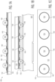
- FIG. 1A shows an example environment 100 in which substrate 110 (e.g., an electronic device substrate such as a semiconductor die) provided with metalized pads 140 disposed within and above an electrically insulating passivation material 130 and so-called repassivation material 132.
- the substrate 110 is further provided with volumes of soldering material (solder bumps 150) which are metallurgically bonded (and as such, electrically coupled) to the metalized pads 140.
- the substrate 110 is protected by a passivation material 130 which can be selectively patterned to allow the deposition of electrical contact pads (not shown) or to expose previously formed contacts, leaving the rest of the substrate protected.
- a second passivation layer (the repassivation material 132) is typically formed above a layer of the passivation material 130 and has a lower modulus of elasticity (Young's modulus) than the passivation material 130. This can be desirable in substrates intended to be bonded to chip carriers or other structures in order to reduce the risk of damage to the substrate when pressure is applied during bonding processes as discussed further below.
- the metalized pads have a topography that forms recessed "cups" with edges that are disposed over the passivation material 130 and the repassivation material 132, within which the solder bumps 150 rest on top of the substrate 110. These recessed area can be useful to keep solid beads in place after being placed on the substrate 110 (prior to heating the substrate 110 to reflow the solder), As illustrated, the substrate 110 may be rotated such that the solder bumps 150 face another substrate 190 having metalized pads 195 to which the solder bumps 150 may be metallurgically bonded (e.g., by heating and reflowing of the solder bumps 150), thereby bonding (and electrically coupling) the metalized pads 140 of the substrate 110 to corresponding metalized pads 195 of the substrate 190.
- the substrate 110 may be a semiconductor die configured to be bonded (and also electrically coupled) to a printed circuit board in order to integrate circuitry within the substrate 110 with other circuitry bonded to the substrate 190 or otherwise electrically coupled to the substrate 190.
- FIG. 1C shows a plan view of the portion of the substrate 110 shown in FIG. 1A .
- the solder bumps 150 of FIG. 1A can be seen disposed within the boundaries of the metalized pads 140 which are surrounded by the repassivation material 132. It will be understood that the illustrations described above are schematic in nature and do not necessarily represent the actual shape of solder bumps once properly bonded to a substrate. For instance, it will be understood that once sufficiently heated, a solder bump will tend to melt and wet the surface of a metalized pad on which it rests, similarly to the solder bump depicted in FIG. 2 .
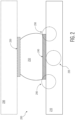
- FIG. 2 depicts a cross-section of an example of a known structure 200 in which solder bump 250 (e.g., a solder bump 150) that is metallurgically bonded to a metalized pad 240 on a substrate 210 and to another substrate 298 (e.g., a printed circuit board) via a metalized pad 299 on that substrate.
- solder bump 250 e.g., a solder bump 150
- another substrate 298 e.g., a printed circuit board
- the soldering material forming the solder bump 250 may be placed on top of the metalized pad 240 in solid form (e.g., as pellet or ball of solder).
- the substrate 210 may then be heated to a suitable reflow temperature (for instance 220°C, as a nonlimiting example), whereupon the solder flows causing its shape to conform to the geometry of the underlying metalized pad.
- the solder and the substrate then cool to ambient temperature, whereupon the solder material solidifies, metallurgically bonding the soldering material to the substrate 210 and forming the solder bump 250 as shown.
- the entire structure may then be bonded to another substrate (e.g., the substrate 298 shown in FIG. 2 ) by way of one or more solder bumps 250.
- mechanical stresses are induced as a solder bump 250 and the substrate 210 coo after being heated during the bonding process.
- solder bump 250 is depicted schematically for purposes of illustration and that the exact shape of a solder bump used to bond two substrates may differ from the shape of the solder bump 250 as shown in FIG. 2 .
- embodiments herein include structures and methods to provide electronic device substrates with metalized pads which are configured and arranged to reduce mechanical stresses at the interface between an electronic device substrate and solder bumps which are metallurgically bonded to such substrates.
- metalized pads which are configured and arranged to reduce mechanical stresses at the interface between an electronic device substrate and solder bumps which are metallurgically bonded to such substrates.
- the example embodiments and related embodiments may confer certain benefits including, for instance, reducing or preventing stresses in the vicinity of a solder bump; that is, at the interface between the solder bump and a substrate to which it is bonded, and/or in an underlying semiconductor die, when compared with bonding solder bumps to substrates using metalized pads fabricated according to previous approaches (e.g., as illustrated and described above in FIGs. 1A-1C and FIG. 2 ).
- metalized pads according to embodiments herein described below can enable reduced peeling stresses at the interface between a solder bump and a metalized pad, thereby reducing the incidence of crack formation induced between solder bump and a semiconductor die or other device substrate.
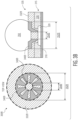
- FIG. 3A shows plan view a cross-sectional schematic view of an example structure 300A according to embodiments herein.
- a substrate 310 e.g., a substrate 110/210
- contacts 320 e.g., a metal contact electrically coupled to one or more electronic devices within the substrate 310.
- Each contact 320 (and other structures on or near the surface 315 of the substrate 310) are protected by a first electrically insulating material (which may be referred to as a "passivation,” “passivation material,” or a “passivation layer” 330) and a second electrically insulating material 332A (which may be referred to as a "repassivation,” “repassivation material,” or a repassivation material” 332A).
- the repassivation material 332A forms a substantially planar surface 335 above the top surface 315 of the substrate 310.
- One or more metalized pads 340A are disposed within the substantially planar surface 335 and are electrically coupled to a corresponding contact 320 through an aperture in the passivation material 330 and the repassivation material 332A. As shown, the metalized pad 340A is surrounded by the repassivation material 332A and is coplanar with the repassivation material 332A along an outer boundary region that is partially defined by the diameter 352A relative to a central region 349A defined by the dimension 352A. As shown the metalized pad 340A is recessed below the planar surface 335 of the repassivation material 332A within the central region 349A above the contact 320 indicated by the dimension 354A. However, it will be appreciated that, in one or more related embodiments, the recessed area is not required.
- FIG. 3B shows plan view a cross-sectional schematic view of an example structure 300B that is an alternative to the structure 300A in one or more embodiments.
- the metalized pad 340B is patterned inversely to the metalized pad 340A. That is, the metalized pad 340B surrounds a central area 349B (indicated by the dimension 352B) where the metallization is absent and includes an interior region in which the metalized pad 340B and the repassivation material 332B (e.g., the repassivation material 332A).
- the structure 300B When compared to the structure 300A, the structure 300B may have lower thermal and electrical conductivity, making it suitable for applications in which thermal power dissipation is lower compared to applications for which the structure 300A is suited.
- repassivation material e.g., the repassivation material 332B
- an adjacent portion of a metalized pad e.g., the metalized pad 340B
- the recessed area is not required.
- the passivation material 330 and the repassivation material(s) 332A,332B may be any suitable materials.
- the passivation material is a crystalline, semicrystalline, or amorphous oxide or nitride material (e.g., SiO2, SiOX where x is a number other than two, Si3N4, or Si3NX where x is a number other than four, as nonlimiting examples).
- the repassivation material 332A or the repassivation material 332B is a dielectric material with a low elastic modulus compared to the elastic modulus of the repassivation material 332 (e.g., polyimide, polybenzoxazole, etc., as nonlimiting examples).
- metalized pads 340A, 340B may be formed from any suitable materials and by any suitable process(es).
- metalized pads 340A or 340B have a metal surface that is wettable by one or more solder materials (i.e., the surface is "solderable").
- metalized pads 340A or 340B are formed by a stack of two or more electrically conductive materials.
- a metalized pad may include one or more conductive adhesion layers (e.g., Ti, Ni, Ti/Cr as nonlimiting examples) covered by another conductive material such as Cu or Au, as nonlimiting examples.
- the topmost metallization material which will contact a solder bump may be chosen to have favorable properties such as being easily wetted by a chosen solder material in a molten state.
- FIG. 4 illustrates formation of the structure 300A on the substrate 110 during various steps of an example process 400 having steps 410, 420, 430, 440, 450, 460, 470, and 480.
- the substrate 310 is shown already provided with contact pads 320, the passivation material 330 and the repassivation material 332.
- These contact pads 320 may be any suitable conductive material (e.g., aluminum, copper, gold, etc.) and may be coupled to vias in the substrate 310 or exposed electrical traces on the surface of the substrate 310.
- a masking material 412 e.g., photoresist
- a seed metallization layer 414 e.g., Ti followed by Ni
- the seed metallization 414 is patterned in a subtractive lift-off process in which the masking material 412 is removed (e.g., by a solvent rinse), leaving the seed metallization 414 only on desired portions of the substrate 310. It will be understood that even though a lift-off process is described for the patterning of the seed metallization 414, any suitable process may be used, including a subtractive process wherein the seed metallization is deposited over the entire surface and then substantively patterned (by an etching process, for example). An inset top view 427 of step 420 is also shown, indicating the positioning of the seed metallization 414.
- additional repassivation material 432 is deposited on the substrate 310 followed by a masking material 434 (e.g., photoresist) which is patterned as shown.
- a masking material 434 e.g., photoresist
- a suitable etching process (e.g., one which does not appreciably etch the seed metallization 414 or etches the seed metallization 414 at a much slower rate than it etches the additional repassivation material 432 and the repassivation material 332) is used to etch portions of the additional repassivation material 432 and the repassivation material 332 leaving an aperture in the repassivation material 332 within which the contact pad 320 is exposed.
- An inset top view 447 of step 440 is also shown, indicating the positioning of the exposed contact 320 relative to the seed metallization 414.
- the masking material 434 has been removed and additional seed metallization material 414 or other suitable metallization material is deposited as metallization material 452 over the initial seed metallization material 414.
- the metallization material 422 may deposited via electroplating, sputtering, or evaporation to a desired thickness.
- another masking material 464 e.g., photoresist
- Additional metallization material 462 may then be deposited in a pattern defined by the masking material 464 using any suitable process including electroplating, sputtering, or thermal evaporation, as nonlimiting examples.
- the masking material 464 is removed and the residual seed metallization 414, which was previously protected by the masking material 464 (shown as the residual metal 466 in step 460), is removed using any suitable process including wet chemical etching, dry plasma etching, or chemical-mechanical polishing, as nonlimiting examples, resulting in the metalized pad 340A, which is coplanar (or substantially coplanar) with the repassivation 332A along its outer edge and recessed below the plane of the repassivation material 332A as shown in FIG. 3A .
- the cross-sectional view of step 470 shown corresponds to a plane indicated by the dashed line 479 that bisects the inset top view 477 of step 470.
- the solder bump 350 is bonded to the metalized pad 340A by any suitable process.
- a solid volume of solder may be placed on the metalized pad and heated until the solder wets the metalized pad and then bonds to the pad upon cooling.
- FIG. 5 illustrates formation of the structure 300B on the substrate 310 during various steps of an example process 500 having steps 510, 520, 530, 540, 550, 560, 570, and 580.
- the substrate 310 is shown already provided with contact pads 320, the passivation material 330 and the repassivation material 332.
- a masking material 512 e.g., masking material 412 is deposited on top of the repassivation material 332 and patterned as shown.
- a seed metallization layer 514 e.g., the seed metallization 414) is deposited over the patterned masking material 512.
- the seed metallization 514 is patterned in a subtractive lift-off process in which the masking material 512 is removed, leaving the seed metallization 414 only on desired portions of the substrate 310. It will be understood that even though a lift-off process is described for the patterning of the seed metallization 414, any suitable process may be used, including a subtractive process wherein the seed metallization is deposited over the entire surface and then substantively patterned (by an etching process, for example). An inset top view 527 of step 520 is also shown, indicating the positioning of the seed metallization 514.
- additional repassivation material 532 e.g., the additional repassivation material 432 is deposited on the substrate 310 followed by deposition of a masking material 532 (the masking material 432) which is patterned as shown.
- the masking material 534 in step 530 covers the seed metallization 514 and also an area between the two areas of seed metallization 514.
- a suitable etching process is used to etch portions of the additional repassivation material 532 and the repassivation material 332 (e.g., as previously described in connection with step 440 of the process 400) leaving apertures in the repassivation material 332 within which the contact pad 320 is exposed.
- the masking material 534 is removed and additional seed metallization material 514 or another additional metallization material is deposited over initial seed metallization 514 as the metallization material 552.
- additional seed metallization material 514 or metallization material 552 may deposited via electroplating, sputtering, or evaporation to a desired thickness, as previously described in connection with step 450 of the process 400.
- another masking material 564 (e.g., the masking material 464 of the process 400) is deposited and patterned, as shown. Additional metallization material 562 may then be deposited in a pattern defined by the masking material 564 using any suitable process, as previously described in connection with step 460 of the process 400.
- the masking material 562 is removed and the residual seed metallization 414, which was previously protected by the masking material 464 (shown as the residual metal 566 in step 560), is removed using any suitable process including wet chemical etching, dry plasma etching, or chemical-mechanical polishing, as nonlimiting examples, resulting in the metalized pad 340B which is coplanar with the repassivation 332B along its outer edge and recessed below the plane of the repassivation material 332B as shown in FIG. 3B .
- the cross-sectional view of step 570 shown corresponds to a plane indicated by the dashed line 579 that bisects the inset top view 577 of step 570.
- masking material 582 e.g., photoresist
- the additional repassivation material 532 in that region is partially removed using any suitable process (e.g., wet etching, or dry plasma etching as nonlimiting examples) to create the recessed profile of the shown in which the additional repassivation material 532 is substantially coplanar with the surrounding recessed portion of the metalized pad 340B.
- any suitable process e.g., wet etching, or dry plasma etching as nonlimiting examples
- the recessed profile shown can be achieved in any suitable manner including performing the step 580 or a similar step at a different point in the process 500.
- the additional repassivation material 532 could be patterned immediately after step 540 as one non-limiting example.
- step 590 e.g., the step 480 of the process 400
- the solder bump 350 is bonded to the metalized pad 340B by any suitable process, as previously described in connection with step 480 of the process 400.
- the masking material 512 may be patterned such that an additional segment of the seed metallization 514 is present on the surface of the repassivation material 332 at subsequent steps 520, 530, and 540.
- processes 400 and 500 as shown in FIG. 4 and FIG. 5 respectively are described as having various patterning steps which involve patterning one or masking materials (e.g., photoresist) that, in some instances, areas of the repassivation material (e.g., additional repassivation material 432, 532 and/or repassivation material 332) may be patterned directly using known lithographic techniques to selectively cross-link or depolymerize the repassivation materials.
- one or masking materials e.g., photoresist
- areas of the repassivation material e.g., additional repassivation material 432, 532 and/or repassivation material 332
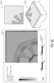
- FIG. 6A includes a plot 600A showing the result of computational simulations of the peeling stresses (stresses that are concentrated at edges when two materials are bonded together) on the surface of semiconductor provided with a conventionally-shaped metalized pad with a non-planar topography (e.g., a metalized pad 140 as shown in FIG. 1A and FIG. 1B ) when a solder ball (e.g., a solder ball 150) is joined to the metalized pads.
- a concentrated annular area 610A of high peeling stress values can be seen. Note that only one quadrant is simulated, as shown by the schematic top view illustration 602A.
- An isometric view 604A shows that the simulated structure is not coplanar with the surrounding repassivation material
- FIG. 6B includes a plot 600B showing the result of computational simulations of the peeling stresses on the surface of semiconductor die provided with metalized pad that is patterned similarly to the metalized pad 340A but without the planarized topography present in embodiments herein (e.g., the metalized pad 340A). Areas of high peeling stresses are present in the annular region 610B (analogous to the annular region 610A), but areas of reduced stress (indicated by dashed ellipses) are seen within the annular region 610B. The peak peeling stress in the simulation represented by the plot 600B is reduced by approximately 7% compared to the simulation represented by the plot of FIG. 6A . As above only one quadrant is simulated, as shown by the schematic top view illustration 602B. An isometric view 604B shows that the simulated pad structure is not coplanar with the surrounding repassivation material.
- FIG. 6C includes a plot 600C showing the result of computational simulations of the peeling stresses on the surface of semiconductor die provided with a metalized pad according to embodiments herein (i.e., a pad similar to the metalized pad 340A) Areas of high peeling stresses are present in the annular region 610C (analogous to the annular regions 610A and 610B) and areas of reduced stress (indicated by dashed ellipses) are present as in the annular region 610B. But it can be seen that the combination of a shaped metalized pad and coplanarity of the pad with the surrounding repassivation material can result in significantly reduced peak values for the peeling stresses.
- FIG. 6C is reduced by approximately 44% compared to the simulation represented by the plot 600A of FIG. 6A .
- only one quadrant is simulated, as shown by the schematic top view illustration 602C.
- An isometric view 604C shows that the simulated pad structure, in contrast to the structures of FIG. 6A and FIG. 6B , is coplanar with the surrounding repassivation material at its outer boundary with the repassivation material.
- metalized pads that are patterned to have an interdigitated arrangement with a repassivation layer it should be understood that other patterns can be used in one or more embodiments.
- suitable metalized pads are shown in FIG. 7 and include annular structures 702, 704, and 706; a slotted annular structure 708; a Greek cross 712 and a separated Greek cross 714; and an inverted trefoil 716. It will be understood that nothing herein is intended to limit the topology of metalized pads according to embodiments to any particular number or types of patterns.
- one or more embodiments may include recessed areas such as those shown in FIG. 3A and FIG. 3B , that in one or more other embodiments, such recessed areas can be omitted.
Landscapes
- Internal Circuitry In Semiconductor Integrated Circuit Devices (AREA)
- Engineering & Computer Science (AREA)
- Manufacturing & Machinery (AREA)
Abstract
Description
- Embodiments of the subject matter described herein relate to structures and methods for flip-chip bonding of electronic devices.
- In flip-chip bonding a semiconductor die is provided with metal surface contacts disposed at the bottom of openings in a layer of passivation material that protects the surface of the die. Additional passivation materials and metalized structures are added to create external metal pads surrounded by passivation material such that the surface of the semiconductor die is completely covered and protected. The external metal pads are configured to allow selective bonding of solder materials to the external metal pads, resulting in solder balls or "bumps" on a top surface of the die. Semiconductor die having such solder bumps may then be inverted and bonded face-down to pads on a circuit board or other surface via the solder bumps
- In an example embodiment, an electronic device substrate is provided. The substrate includes a repassivation material layer having a substantially planar surface formed on the substrate from a first electrically nonconductive material. The substrate also includes a metalized pad surrounded by and coplanar with the first electrically nonconductive material along an outer boundary of the metalized pad. The metalized pad has a solderable surface and electrically contacts an electrical contact pad on the substrate beneath the metalized pad.
- In an example embodiment, a method of fabricating a semiconductor device is provided. The method includes forming a repassivation material layer having a substantially planar surface on a substrate from a first electrically nonconductive material above a substrate having an electrical contact pad. The method also includes forming an aperture in the repassivation material layer that exposes an electrical contact pad on the substrate. The method also includes forming, within the aperture, a metalized pad that is surrounded by and coplanar with the repassivation material layer along an edge of the aperture, wherein the metalized pad has a solderable surface and electrically contacts the electrical contact pad
- The present disclosure is illustrated by way of examples, embodiments and the like and is not limited by the accompanying figures, in which like reference numbers indicate similar elements. Elements in the figures are illustrated for simplicity and clarity and have not necessarily been drawn to scale. The figures along with the detailed description are incorporated and form part of the specification and serve to further illustrate examples, embodiments and the like, and explain various principles and advantages, in accordance with the present disclosure, wherein:
-
FIG. 1A shows example semiconductor substrate provided with solder bumps suitable for flip-chip bonding of the substrate to another substrate such as a printed circuit board. -
FIG. 1B shows the substrate ofFIG. 1A bonded to another substrate (such as a printed circuit board via the solder bumps ofFIG. 1A . -
FIG. 1C is a top view of the substrate ofFIG. 1A showing the solder bumps and surrounding metalized pads. -
FIG. 2 shows a cross-sectional view of a solder bump bonded to metalized pad on a semiconductor substrate illustrating areas of tensile and compressive stresses formed in the solder bump and the substrate following bonding of the solder bump to the metalized pad on the substrate and bonding of the substrate to another substrate (such as a printed circuit board) via the solder bump. -
FIG. 3A shows a schematic plan view and a schematic cross-sectional view of a portion of an electronic device substrate provided with a patterned metalized pad configured to be bonded to a solder bump according to embodiments herein. -
FIG. 3B shows a schematic plan view and a schematic cross-sectional view of a portion of an electronic device substrate provided with another type patterned metalized pad configured to be bonded to a solder bump according to embodiments herein. -
FIG. 4 is flow diagram illustrating a formation of the metalized pad ofFIG. 4 during various steps in an example fabrication process according to embodiments herein. -
FIG. 5 is a flow diagram illustrating a formation of the metalized pad ofFIG. 5 during various steps in an example fabrication process according to embodiments herein. -
FIG. 6A is a representation of the result of computational simulations of peeling stresses in a conventional metalized pad bonded to a solder bump as shown inFIG. 1A , in a metalized pad without the coplanar arrangement shown inFIG. 3A andFIG. 3B , and in the structure ofFIG. 3A according to embodiments herein -
FIG. 6B represents the result of computational simulations of peeling stresses in a metalized pad that has a similar pattern to embodiments herein but lacking the coplanar arrangement shown inFIG. 3A andFIG. 3B , and in the structure ofFIG. 3A . according to embodiments herein. -
FIG. 6C represents the result of computational simulations of peeling stresses in a metalized pad bonded to a solder bump as shown inFIG. 3A according to embodiments herein which is both patterned and coplanar with the surrounding repassivation material as described herein. - The following detailed description provides examples for the purposes of understanding and is not intended to limit the invention or the application and uses of the same. Furthermore, there is no intention to be bound by any expressed or implied theory presented in the preceding technical field, background, or the following detailed description.
- For simplicity and clarity of illustration, the drawing figures illustrate the general manner of construction, and descriptions and details of well-known features and techniques may be omitted to avoid unnecessarily obscuring the invention. Additionally, elements in the drawing figures are not necessarily drawn to scale. For example, the dimensions of some of the elements or regions in the figures may be exaggerated relative to other elements or regions to help improve understanding of embodiments of the invention.
- The terms "first," "second," "third," "fourth" and the like in the description and the claims, if any, may be used for distinguishing between similar elements and not necessarily for describing a particular sequential or chronological order. It is to be understood that the terms so used are interchangeable under appropriate circumstances such that the embodiments of the invention described herein are, for example, capable of operation in sequences other than those illustrated or otherwise described herein. Furthermore, the terms "comprise," "include," "have" and any variations thereof, are intended to cover non-exclusive inclusions, such that a process, method, article, or apparatus that comprises a list of elements is not necessarily limited to those elements but may include other elements not expressly listed or inherent to such process, method, article, or apparatus. The term "coupled," as used herein, is defined as directly or indirectly connected in an electrical or non-electrical manner. As used herein the terms "substantial" and "substantially" mean sufficient to accomplish the stated purpose in a practical manner and that minor imperfections, if any, are not significant for the stated purpose. As a nonlimiting example, "substantially planar" may mean "planar having a deviation of no more than plus or
minus 100 µm from a mean level", or "planar having a deviation of no more than plus and minus 20 µm from a mean level". Furthermore, a "substantially planar surface" may refer to a local region underneath an individual solder ball or bump on a top surface of the die. The substantially planar surface between themetallized pads 340A andrepassivation 332A may have a deviation of no more than 25% of therepassivation 332A thickness ormetallized pads 340A thickness, whichever is smaller. Deviation in substantially planar region will typically be in the order of a few µms. Lower deviation in the substantially planar surface will result in lower peel stress. Substantially planar surface beneath individual solder balls or bumps within a die, may have a deviation of up to 10 µm. Moreover, "substantially planar" may include "planar" - Directional references such as "top," "bottom," "left," "right," "above," "below," and so forth, unless otherwise stated, are not intended to require any preferred orientation and are made with reference to the orientation of the corresponding figure or figures for purposes of illustration.
-
FIG. 1A shows anexample environment 100 in which substrate 110 (e.g., an electronic device substrate such as a semiconductor die) provided with metalizedpads 140 disposed within and above an electrically insulatingpassivation material 130 and so-calledrepassivation material 132. Thesubstrate 110 is further provided with volumes of soldering material (solder bumps 150) which are metallurgically bonded (and as such, electrically coupled) to the metalizedpads 140. Thesubstrate 110 is protected by apassivation material 130 which can be selectively patterned to allow the deposition of electrical contact pads (not shown) or to expose previously formed contacts, leaving the rest of the substrate protected. A second passivation layer (the repassivation material 132) is typically formed above a layer of thepassivation material 130 and has a lower modulus of elasticity (Young's modulus) than thepassivation material 130. This can be desirable in substrates intended to be bonded to chip carriers or other structures in order to reduce the risk of damage to the substrate when pressure is applied during bonding processes as discussed further below. - As shown, the metalized pads have a topography that forms recessed "cups" with edges that are disposed over the
passivation material 130 and therepassivation material 132, within which the solder bumps 150 rest on top of thesubstrate 110. These recessed area can be useful to keep solid beads in place after being placed on the substrate 110 (prior to heating thesubstrate 110 to reflow the solder), As illustrated, thesubstrate 110 may be rotated such that the solder bumps 150 face anothersubstrate 190 having metalizedpads 195 to which the solder bumps 150 may be metallurgically bonded (e.g., by heating and reflowing of the solder bumps 150), thereby bonding (and electrically coupling) the metalizedpads 140 of thesubstrate 110 to corresponding metalizedpads 195 of thesubstrate 190. As an example, thesubstrate 110 may be a semiconductor die configured to be bonded (and also electrically coupled) to a printed circuit board in order to integrate circuitry within thesubstrate 110 with other circuitry bonded to thesubstrate 190 or otherwise electrically coupled to thesubstrate 190.FIG. 1C shows a plan view of the portion of thesubstrate 110 shown inFIG. 1A . The solder bumps 150 ofFIG. 1A can be seen disposed within the boundaries of the metalizedpads 140 which are surrounded by therepassivation material 132. It will be understood that the illustrations described above are schematic in nature and do not necessarily represent the actual shape of solder bumps once properly bonded to a substrate. For instance, it will be understood that once sufficiently heated, a solder bump will tend to melt and wet the surface of a metalized pad on which it rests, similarly to the solder bump depicted inFIG. 2 . -
FIG. 2 depicts a cross-section of an example of a knownstructure 200 in which solder bump 250 (e.g., a solder bump 150) that is metallurgically bonded to ametalized pad 240 on asubstrate 210 and to another substrate 298 (e.g., a printed circuit board) via ametalized pad 299 on that substrate. In a representative process, the soldering material forming thesolder bump 250 may be placed on top of the metalizedpad 240 in solid form (e.g., as pellet or ball of solder). Thesubstrate 210 may then be heated to a suitable reflow temperature (for instance 220°C, as a nonlimiting example), whereupon the solder flows causing its shape to conform to the geometry of the underlying metalized pad. The solder and the substrate then cool to ambient temperature, whereupon the solder material solidifies, metallurgically bonding the soldering material to thesubstrate 210 and forming thesolder bump 250 as shown. The entire structure may then be bonded to another substrate (e.g., thesubstrate 298 shown inFIG. 2 ) by way of one or more solder bumps 250. In such an example structure, mechanical stresses are induced as asolder bump 250 and thesubstrate 210 coo after being heated during the bonding process. In theexample structure 200 and related structures, areas of high tensile stress within thesubstrate 210 will tend to form in theregions 290 beneath the edges of thesolder bump 250 while areas of high compressive stress will tend to form in the die in theregion 295 beneath the center of thesolder bump 250 as wells as tensile stresses in the solder bump itself in the vicinity of theregions solder bump 250. It will be understood that thesolder bump 250 is depicted schematically for purposes of illustration and that the exact shape of a solder bump used to bond two substrates may differ from the shape of thesolder bump 250 as shown inFIG. 2 . - Accordingly, as illustrated in
FIG. 3A andFIG. 3B , embodiments herein include structures and methods to provide electronic device substrates with metalized pads which are configured and arranged to reduce mechanical stresses at the interface between an electronic device substrate and solder bumps which are metallurgically bonded to such substrates. As will be explained below in connection withFIG. 6A ,FIG. 6B , andFIG. 6C , the example embodiments and related embodiments may confer certain benefits including, for instance, reducing or preventing stresses in the vicinity of a solder bump; that is, at the interface between the solder bump and a substrate to which it is bonded, and/or in an underlying semiconductor die, when compared with bonding solder bumps to substrates using metalized pads fabricated according to previous approaches (e.g., as illustrated and described above inFIGs. 1A-1C andFIG. 2 ). In particular the process of bonding a solder bump to metalized pad as shown inFIG. 2 tends to induce cracks that originate at the edges of the metalized pad. Metalized pads according to embodiments herein described below can enable reduced peeling stresses at the interface between a solder bump and a metalized pad, thereby reducing the incidence of crack formation induced between solder bump and a semiconductor die or other device substrate. -
FIG. 3A shows plan view a cross-sectional schematic view of anexample structure 300A according to embodiments herein. In theexample structure 300A, a substrate 310 (e.g., asubstrate 110/210) includes one or more contacts 320 (e.g., a metal contact electrically coupled to one or more electronic devices within the substrate 310). Each contact 320 (and other structures on or near thesurface 315 of the substrate 310) are protected by a first electrically insulating material (which may be referred to as a "passivation," "passivation material," or a "passivation layer" 330) and a second electrically insulatingmaterial 332A (which may be referred to as a "repassivation," "repassivation material," or a repassivation material" 332A). Therepassivation material 332A forms a substantiallyplanar surface 335 above thetop surface 315 of thesubstrate 310. One ormore metalized pads 340A are disposed within the substantiallyplanar surface 335 and are electrically coupled to acorresponding contact 320 through an aperture in thepassivation material 330 and therepassivation material 332A. As shown, themetalized pad 340A is surrounded by therepassivation material 332A and is coplanar with therepassivation material 332A along an outer boundary region that is partially defined by thediameter 352A relative to acentral region 349A defined by thedimension 352A. As shown the metalizedpad 340A is recessed below theplanar surface 335 of therepassivation material 332A within thecentral region 349A above thecontact 320 indicated by thedimension 354A. However, it will be appreciated that, in one or more related embodiments, the recessed area is not required. -
FIG. 3B shows plan view a cross-sectional schematic view of anexample structure 300B that is an alternative to thestructure 300A in one or more embodiments. In thestructure 300B, themetalized pad 340B is patterned inversely to the metalizedpad 340A. That is, themetalized pad 340B surrounds acentral area 349B (indicated by thedimension 352B) where the metallization is absent and includes an interior region in which the metalizedpad 340B and therepassivation material 332B (e.g., therepassivation material 332A). When compared to thestructure 300A, thestructure 300B may have lower thermal and electrical conductivity, making it suitable for applications in which thermal power dissipation is lower compared to applications for which thestructure 300A is suited. It will be understood that, in one or more embodiments, repassivation material (e.g., therepassivation material 332B) and an adjacent portion of a metalized pad (e.g., themetalized pad 340B) are recessed below the substantiallyplanar surface 335, as depicted in the cross-sectional view inFIG. 3B of thestructure 300B. As above, it will be appreciated that, in one or more related embodiments, the recessed area is not required. - The
passivation material 330 and the repassivation material(s) 332A,332B may be any suitable materials. In one or more embodiments, the passivation material is a crystalline, semicrystalline, or amorphous oxide or nitride material (e.g., SiO2, SiOX where x is a number other than two, Si3N4, or Si3NX where x is a number other than four, as nonlimiting examples). In one or more embodiments, therepassivation material 332A or therepassivation material 332B is a dielectric material with a low elastic modulus compared to the elastic modulus of the repassivation material 332 (e.g., polyimide, polybenzoxazole, etc., as nonlimiting examples). Similarly, the metalizedpads pads pads -
FIG. 4 illustrates formation of thestructure 300A on thesubstrate 110 during various steps of anexample process 400 havingsteps step 410, thesubstrate 310 is shown already provided withcontact pads 320, thepassivation material 330 and therepassivation material 332. Thesecontact pads 320 may be any suitable conductive material (e.g., aluminum, copper, gold, etc.) and may be coupled to vias in thesubstrate 310 or exposed electrical traces on the surface of thesubstrate 310. In the example ofstep 410, a masking material 412 (e.g., photoresist) is deposited on top of therepassivation material 332 and patterned as shown. A seed metallization layer 414 (e.g., Ti followed by Ni) is deposited over patterned masking material 412 (e.g., photoresist). - At
step 420, theseed metallization 414 is patterned in a subtractive lift-off process in which the maskingmaterial 412 is removed (e.g., by a solvent rinse), leaving theseed metallization 414 only on desired portions of thesubstrate 310. It will be understood that even though a lift-off process is described for the patterning of theseed metallization 414, any suitable process may be used, including a subtractive process wherein the seed metallization is deposited over the entire surface and then substantively patterned (by an etching process, for example). An insettop view 427 ofstep 420 is also shown, indicating the positioning of theseed metallization 414. - At
step 430,additional repassivation material 432 is deposited on thesubstrate 310 followed by a masking material 434 (e.g., photoresist) which is patterned as shown. - At
step 440, a suitable etching process (e.g., one which does not appreciably etch theseed metallization 414 or etches theseed metallization 414 at a much slower rate than it etches theadditional repassivation material 432 and the repassivation material 332) is used to etch portions of theadditional repassivation material 432 and therepassivation material 332 leaving an aperture in therepassivation material 332 within which thecontact pad 320 is exposed. An insettop view 447 ofstep 440 is also shown, indicating the positioning of the exposedcontact 320 relative to theseed metallization 414. - At
step 450, the maskingmaterial 434 has been removed and additionalseed metallization material 414 or other suitable metallization material is deposited asmetallization material 452 over the initialseed metallization material 414. As an example, the metallization material 422 may deposited via electroplating, sputtering, or evaporation to a desired thickness. - At
step 460, another masking material 464 (e.g., photoresist) is deposited and patterned, as shown.Additional metallization material 462 may then be deposited in a pattern defined by the masking material 464 using any suitable process including electroplating, sputtering, or thermal evaporation, as nonlimiting examples. - At
step 470, the masking material 464 is removed and theresidual seed metallization 414, which was previously protected by the masking material 464 (shown as theresidual metal 466 in step 460), is removed using any suitable process including wet chemical etching, dry plasma etching, or chemical-mechanical polishing, as nonlimiting examples, resulting in the metalizedpad 340A, which is coplanar (or substantially coplanar) with therepassivation 332A along its outer edge and recessed below the plane of therepassivation material 332A as shown inFIG. 3A . The cross-sectional view ofstep 470 shown corresponds to a plane indicated by the dashedline 479 that bisects the insettop view 477 ofstep 470. - Finally, at
step 480, thesolder bump 350 is bonded to the metalizedpad 340A by any suitable process. For example, a solid volume of solder may be placed on the metalized pad and heated until the solder wets the metalized pad and then bonds to the pad upon cooling. -
FIG. 5 illustrates formation of thestructure 300B on thesubstrate 310 during various steps of anexample process 500 havingsteps step 510, thesubstrate 310 is shown already provided withcontact pads 320, thepassivation material 330 and therepassivation material 332. In the example ofstep 510, a masking material 512 (e.g., masking material 412) is deposited on top of therepassivation material 332 and patterned as shown. A seed metallization layer 514 (e.g., the seed metallization 414) is deposited over the patternedmasking material 512. - At step 520 (e.g., the
step 420 of the process 400), theseed metallization 514 is patterned in a subtractive lift-off process in which the maskingmaterial 512 is removed, leaving theseed metallization 414 only on desired portions of thesubstrate 310. It will be understood that even though a lift-off process is described for the patterning of theseed metallization 414, any suitable process may be used, including a subtractive process wherein the seed metallization is deposited over the entire surface and then substantively patterned (by an etching process, for example). An insettop view 527 ofstep 520 is also shown, indicating the positioning of theseed metallization 514. - At
step 530, additional repassivation material 532 (e.g., the additional repassivation material 432) is deposited on thesubstrate 310 followed by deposition of a masking material 532 (the masking material 432) which is patterned as shown. In contrast to step 430 of theprocess 400, the maskingmaterial 534 instep 530 covers theseed metallization 514 and also an area between the two areas ofseed metallization 514. - At
step 540, a suitable etching process is used to etch portions of theadditional repassivation material 532 and the repassivation material 332 (e.g., as previously described in connection withstep 440 of the process 400) leaving apertures in therepassivation material 332 within which thecontact pad 320 is exposed. - At
step 550, the maskingmaterial 534 is removed and additionalseed metallization material 514 or another additional metallization material is deposited overinitial seed metallization 514 as themetallization material 552. As an example,metallization material 514 ormetallization material 552 may deposited via electroplating, sputtering, or evaporation to a desired thickness, as previously described in connection withstep 450 of theprocess 400. - At
step 560, another masking material 564 (e.g., the masking material 464 of the process 400) is deposited and patterned, as shown.Additional metallization material 562 may then be deposited in a pattern defined by the maskingmaterial 564 using any suitable process, as previously described in connection withstep 460 of theprocess 400. - At
step 570, the maskingmaterial 562 is removed and theresidual seed metallization 414, which was previously protected by the masking material 464 (shown as theresidual metal 566 in step 560), is removed using any suitable process including wet chemical etching, dry plasma etching, or chemical-mechanical polishing, as nonlimiting examples, resulting in the metalizedpad 340B which is coplanar with therepassivation 332B along its outer edge and recessed below the plane of therepassivation material 332B as shown inFIG. 3B . The cross-sectional view ofstep 570 shown corresponds to a plane indicated by the dashedline 579 that bisects the insettop view 577 ofstep 570. - At
step 580, masking material 582 (e.g., photoresist) is patterned over the center of the metalizedpad 340B and theadditional repassivation material 532 in that region is partially removed using any suitable process (e.g., wet etching, or dry plasma etching as nonlimiting examples) to create the recessed profile of the shown in which theadditional repassivation material 532 is substantially coplanar with the surrounding recessed portion of the metalizedpad 340B. It will be appreciated that, in one or more embodiments, the recessed profile shown can be achieved in any suitable manner including performing thestep 580 or a similar step at a different point in theprocess 500. For example, theadditional repassivation material 532 could be patterned immediately afterstep 540 as one non-limiting example. - Finally, at step 590 (e.g., the
step 480 of the process 400), after the maskingmaterial 582 has been removed, thesolder bump 350 is bonded to the metalizedpad 340B by any suitable process, as previously described in connection withstep 480 of theprocess 400. - It will further be appreciated that, in or more embodiments, modifications to various steps shown may be employed. For instance, at
step 510, the maskingmaterial 512 may be patterned such that an additional segment of theseed metallization 514 is present on the surface of therepassivation material 332 atsubsequent steps - It will also be appreciated that although
processes FIG. 4 andFIG. 5 , respectively are described as having various patterning steps which involve patterning one or masking materials (e.g., photoresist) that, in some instances, areas of the repassivation material (e.g.,additional repassivation material -
FIG. 6A includes aplot 600A showing the result of computational simulations of the peeling stresses (stresses that are concentrated at edges when two materials are bonded together) on the surface of semiconductor provided with a conventionally-shaped metalized pad with a non-planar topography (e.g., ametalized pad 140 as shown inFIG. 1A and FIG. 1B ) when a solder ball (e.g., a solder ball 150) is joined to the metalized pads.. A concentratedannular area 610A of high peeling stress values can be seen. Note that only one quadrant is simulated, as shown by the schematictop view illustration 602A. Anisometric view 604A shows that the simulated structure is not coplanar with the surrounding repassivation material -
FIG. 6B includes aplot 600B showing the result of computational simulations of the peeling stresses on the surface of semiconductor die provided with metalized pad that is patterned similarly to the metalizedpad 340A but without the planarized topography present in embodiments herein (e.g., themetalized pad 340A). Areas of high peeling stresses are present in theannular region 610B (analogous to theannular region 610A), but areas of reduced stress (indicated by dashed ellipses) are seen within theannular region 610B. The peak peeling stress in the simulation represented by theplot 600B is reduced by approximately 7% compared to the simulation represented by the plot ofFIG. 6A . As above only one quadrant is simulated, as shown by the schematictop view illustration 602B. Anisometric view 604B shows that the simulated pad structure is not coplanar with the surrounding repassivation material. -
FIG. 6C includes aplot 600C showing the result of computational simulations of the peeling stresses on the surface of semiconductor die provided with a metalized pad according to embodiments herein (i.e., a pad similar to the metalizedpad 340A) Areas of high peeling stresses are present in theannular region 610C (analogous to theannular regions annular region 610B. But it can be seen that the combination of a shaped metalized pad and coplanarity of the pad with the surrounding repassivation material can result in significantly reduced peak values for the peeling stresses. The peak peeling stress in the simulation represented by theplot 600C ofFIG. 6C is reduced by approximately 44% compared to the simulation represented by theplot 600A ofFIG. 6A . As above, only one quadrant is simulated, as shown by the schematictop view illustration 602C. Anisometric view 604C shows that the simulated pad structure, in contrast to the structures ofFIG. 6A andFIG. 6B , is coplanar with the surrounding repassivation material at its outer boundary with the repassivation material. - Although various illustrations and examples herein describe metalized pads that are patterned to have an interdigitated arrangement with a repassivation layer it should be understood that other patterns can be used in one or more embodiments. Non-limiting examples of suitably patterned metalized pads are shown in
FIG. 7 and includeannular structures annular structure 708; aGreek cross 712 and a separatedGreek cross 714; and aninverted trefoil 716. It will be understood that nothing herein is intended to limit the topology of metalized pads according to embodiments to any particular number or types of patterns. Additionally, it will be understood that although one or more embodiments may include recessed areas such as those shown inFIG. 3A andFIG. 3B , that in one or more other embodiments, such recessed areas can be omitted. - It will be appreciated that the steps of various processes described herein are nonlimiting examples of suitable processes according to embodiments and are for the purposes of illustration. Systems and devices according to embodiments herein may use any suitable processes including those that omit steps described herein, perform those steps and similar steps in different orders, and the like. It will also be appreciated that well-known steps or other well-known process features may be omitted for clarity.
- Features of embodiments may be understood by way of one or more of the following examples:
- Example 1: An electronic device substrate includes a repassivation material layer and a metalized pad. The repassivation material layer has a substantially planar surface formed on the substrate from a first electrically nonconductive material and the metalized pad is surrounded by and coplanar with the first electrically nonconductive material along an outer boundary of the metalized pad. The metalized pad has a solderable surface and electrically contacts an electrical contact pad on the substrate beneath the metalized pad.
- Example 2: The substrate of Example 1, in which the metalized pad includes metalized fingers that extend radially from the outer boundary of the metalized pad in interdigitated arrangement with the repassivation material layer.
- Example 3: The substrate of Example 2 in which the metalized fingers of the metalized pad extend radially outward from a central portion of the metalized pad.
- Example 4: The substrate of any of Examples 1-3, in which the metalized pad includes a recessed portion inside the outer boundary that is recessed below the substantially planar surface.
- Example 5: The substrate of any of Examples 2-4, in which the metalized fingers of the metalized pad extend radially inward from the outer boundary of the metalized pad toward a central region formed from the first electrically nonconductive material of the repassivation material layer.
- Example 6: The substrate of Example 5, in which a portion of each metalized finger includes a recessed portion inside the outer boundary that is recessed below the substantially planar surface. The central region formed from the first electrically nonconductive material of the repassivation material layer is also recessed below the substantially planar surface and is substantially coplanar with the recessed portion of each metalized finger.
- Example 7: The substrate of any of Examples 1-6, in which the metalized pad includes a recessed portion inside the outer boundary that is recessed below the substantially planar surface.
- Example 8: The substrate of any of Examples 1-7. The electronic device substrate of
claim 2, further comprising a passivation material layer formed from a second electrically nonconductive material underlying the substantially planar surface of the repassivation material layer. - Example 9: The substrate of Example 8, in which the first electrically nonconductive material is a polymeric material characterized by a first elastic modulus and the second electrically nonconductive material is characterized by a second elastic modulus that is higher than the first elastic modulus.
- Example 10: The substrate of any of Examples 1-9, further including an electrically conductive contact beneath the metalized pad. The metalized pad is electrically coupled to the electrically conductive contact within an aperture that passes through the repassivation material layer and the passivation material layer.
- Example 11: The substrate of any of Examples 1-10 wherein the metalized pad and first electrically nonconductive material of the repassivation material are jointly configured and arranged such that mechanical strain in the metallized pad is at least partially relieved by elastic deformation of the repassivation material layer.
- Example 12: A method of fabricating an electronic device substrate that includes forming a repassivation material layer having a substantially planar surface on a substrate from a first electrically nonconductive material above a substrate having an electrical contact pad. The method further includes. The method further includes forming an aperture in the repassivation material layer that exposes an electrical contact pad on the substrate. The method further includes forming, within the aperture, a metalized pad that is surrounded by and coplanar with the repassivation material layer along an edge of the aperture, wherein the metalized pad has a solderable surface and electrically contacts the electrical contact pad.
- Example 13: The method of Example 12, in which forming the metalized pad includes forming metalized fingers that extend radially from an outer boundary of the metalized pad in an interdigitated arrangement with the repassivation material layer.
- Example 14: The method of Example 13, in which the metalized fingers of the metalized pad extend radially outward from a central portion of the metalized pad.
- Example 15: The method of Example 14 or Example 13, in which forming the metalized pad includes forming a recessed portion of the metalized pad inside the outer boundary that is recessed below the substantially planar surface.
- Example 16: The method of any of Examples 13-15, further including forming a central region from the first electrically nonconductive material of the repassivation material layer. In this example, the metalized fingers of the metalized pad extend radially inward from the outer boundary of the metalized pad toward a central region formed from the first electrically nonconductive material of the repassivation material layer.
- Example 17: The method of any of Examples 13-16, in which forming the metalized fingers includes forming a recessed portion of each metalized finger that is recessed below the substantially planar surface and disposed inside the outer boundary. In this example, the central region formed from the first electrically nonconductive material of the repassivation material layer is also recessed below the substantially planar surface and is coplanar with the recessed portion of each metalized finger.
- Example 18: The method of any of Examples 12-17, in which forming the metalized pad includes forming a recessed portion of the metalized pad that is recessed below the substantially planar surface and disposed inside the outer boundary.
- Example 19: The method of any of Examples 12-18 in which the repassivation material layer is formed over a passivation material layer on the substrate formed from a second electrically nonconductive material. The first electrically nonconductive material is a polymeric material characterized by a first elastic modulus and the second electrically nonconductive material characterized by a second elastic modulus that is higher than the first elastic modulus. This example further includes jointly configuring and arranging the metalized pad and the first electrically nonconductive material of the repassivation material layer such that mechanical strain in the metallized pad is at least partially relieved by elastic deformation of the repassivation material layer.
- Example 20: The method of any of Examples 12-19, further including electrically coupling the metalized pad to the electrical contact pad within the aperture that passes through the repassivation material layer.
- The preceding detailed description and examples are merely illustrative in nature and are not intended to limit the embodiments of the subject matter or the application and uses of such embodiments. As used herein, the word "exemplary" means "serving as an example, instance, or illustration." Any implementation described herein as exemplary is not necessarily to be construed as preferred or advantageous over other implementations. Furthermore, there is no intention to be bound by any expressed or implied theory presented in the preceding technical field, background, or detailed description.
- It should be understood that this invention is not limited in its application to the details of construction and the arrangement of components set forth in the preceding description or illustrated in the accompanying drawings. The invention is capable of other embodiments and of being practiced or of being carried out in various ways. Also, it is to be understood that the phraseology and terminology used herein is for the purpose of description and should not be regarded as limiting. The use of "including," "comprising," or "having" and variations thereof herein is meant to encompass the items listed thereafter and equivalents thereof as well as additional items. Unless specified or limited otherwise, the terms "mounted," "connected," "supported," and "coupled" and variations thereof are used broadly and encompass both direct and indirect mountings, connections, supports, and couplings. Further, "connected" and "coupled" are not restricted to physical or mechanical connections or couplings.
- The preceding discussion is presented to enable a person skilled in the art to make and use embodiments of the invention. Various modifications to the illustrated embodiments will be readily apparent to those skilled in the art, and the generic principles herein can be applied to other embodiments and applications without departing from embodiments of the invention. Thus, embodiments of the invention are not intended to be limited to embodiments shown, but are to be accorded the widest scope consistent with the principles and features disclosed herein. The preceding detailed description is to be read with reference to the figures, in which like elements in different figures have like reference numerals. The Figures, which are not necessarily to scale, depict selected embodiments and are not intended to limit the scope of embodiments of the invention. Skilled artisans will recognize the examples provided herein have many useful alternatives and fall within the scope of embodiments of the invention.
- The connecting lines shown in the various figures contained herein are intended to represent example functional relationships and/or physical couplings between the various elements. It should be noted that many alternative or additional functional relationships or physical connections may be present in one or more embodiments of the subject matter. In addition, certain terminology may also be used herein for the purpose of reference only, and thus are not intended to be limiting, and the terms "first," "second" and other such numerical terms referring to structures do not imply a sequence or order unless clearly indicated by the context.
- The foregoing description refers to elements or nodes or features being "connected" or "coupled" together. As used herein, unless expressly stated otherwise, "connected" means that one element is directly joined to (or directly communicates with) another element, and not necessarily mechanically. Likewise, unless expressly stated otherwise, "coupled" means that one element is directly or indirectly joined to (or directly or indirectly communicates with, electrically or otherwise) another element, and not necessarily mechanically. Thus, although the schematic shown in the figures depict one example arrangement of elements, additional intervening elements, devices, features, or components may be present in one or more embodiments of the depicted subject matter.
Claims (15)
- An electronic device substrate comprising:a repassivation material layer having a substantially planar surface formed on the substrate from a first electrically nonconductive material; anda metalized pad surrounded by and coplanar with the first electrically nonconductive material along an outer boundary of the metalized pad;wherein the metalized pad has a solderable surface and electrically contacts an electrical contact pad on the substrate beneath the metalized pad.
- The electronic device substrate of claim 1,
wherein the metalized pad includes metalized fingers that extend radially from the outer boundary of the metalized pad in interdigitated arrangement with the repassivation material layer. - The electronic device substrate of claim 2,
wherein the metalized fingers of the metalized pad extend radially outward from a central portion of the metalized pad. - The electronic device substrate of claim 3,
wherein the metalized pad includes a recessed portion inside the outer boundary that is recessed below the substantially planar surface. - The electronic device substrate of claim 2,
wherein the metalized fingers of the metalized pad extend radially inward from the outer boundary of the metalized pad toward a central region formed from the first electrically nonconductive material of the repassivation material layer. - The electronic device substrate of claim 5,wherein a portion of each metalized finger includes a recessed portion inside the outer boundary that is recessed below the substantially planar surface; andwherein the central region formed from the first electrically nonconductive material of the repassivation material layer is also recessed below the substantially planar surface and is substantially coplanar with the recessed portion of each metalized finger.
- The electronic device substrate of any of claims 2 to 6,
wherein the metalized pad includes a recessed portion inside the outer boundary that is recessed below the substantially planar surface. - The electronic device substrate of any of claims 2 to 7, further comprising a passivation material layer formed from a second electrically nonconductive material underlying the substantially planar surface of the repassivation material layer.
- The electronic device substrate of claim 8, further comprising an electrically conductive contact beneath the metalized pad;
wherein the metalized pad is electrically coupled to the electrically conductive contact within an aperture that passes through the repassivation material layer and the passivation material layer. - The electronic device substrate of claim 8 or 9,wherein the first electrically nonconductive material is a polymeric material characterized by a first elastic modulus; andwherein the second electrically nonconductive material is an inorganic material characterized by a second elastic modulus that is higher than the first elastic modulus.
- The electronic device substrate of claim 10, further comprising:
wherein the metalized pad and first electrically nonconductive material of the repassivation material are jointly configured and arranged such that mechanical strain in the metallized pad is at least partially relieved by elastic deformation of the repassivation material layer. - A method of fabricating an electronic device substrate, comprisingforming a repassivation material layer having a substantially planar surface on a substrate from a first electrically nonconductive material above a substrate having an electrical contact pad;forming an aperture in the repassivation material layer that exposes an electrical contact pad on the substrate; andforming, within the aperture, a metalized pad that is surrounded by and coplanar with the repassivation material layer along an edge of the aperture, wherein the metalized pad has a solderable surface and electrically contacts the electrical contact pad.
- The method of claim 12,
wherein forming the metalized pad includes forming metalized fingers that extend radially from an outer boundary of the metalized pad in an interdigitated arrangement with the repassivation material layer. - The method of claim 13,
wherein the metalized fingers of the metalized pad extend radially outward from a central portion of the metalized pad. - The method of claim 14,
wherein forming the metalized pad includes forming a recessed portion of the metalized pad inside the outer boundary that is recessed below the substantially planar surface.
Applications Claiming Priority (1)
| Application Number | Priority Date | Filing Date | Title |
|---|---|---|---|
| US17/664,113 US12119316B2 (en) | 2022-05-19 | 2022-05-19 | Patterned and planarized under-bump metallization |
Publications (1)
| Publication Number | Publication Date |
|---|---|
| EP4280265A1 true EP4280265A1 (en) | 2023-11-22 |
Family
ID=86331237
Family Applications (1)
| Application Number | Title | Priority Date | Filing Date |
|---|---|---|---|
| EP23172603.5A Pending EP4280265A1 (en) | 2022-05-19 | 2023-05-10 | Patterned and planarized under-bump metallization |
Country Status (2)
| Country | Link |
|---|---|
| US (1) | US12119316B2 (en) |
| EP (1) | EP4280265A1 (en) |
Citations (5)
| Publication number | Priority date | Publication date | Assignee | Title |
|---|---|---|---|---|
| JPH0513418A (en) * | 1991-07-04 | 1993-01-22 | Mitsubishi Electric Corp | Semiconductor device and manufacturing method thereof |
| US6593220B1 (en) * | 2002-01-03 | 2003-07-15 | Taiwan Semiconductor Manufacturing Company | Elastomer plating mask sealed wafer level package method |
| US20110316154A1 (en) * | 2009-03-19 | 2011-12-29 | Panasonic Corporation | Semiconductor device having semiconductor substrate, and method of manufacturing the same |
| US10331993B1 (en) * | 2011-03-22 | 2019-06-25 | Impinj, Inc. | RFID integrated circuits with large contact pads |
| US20200035585A1 (en) * | 2017-04-27 | 2020-01-30 | International Business Machines Corporation | Multiple sized bump bonds |
Family Cites Families (15)
| Publication number | Priority date | Publication date | Assignee | Title |
|---|---|---|---|---|
| US6077726A (en) | 1998-07-30 | 2000-06-20 | Motorola, Inc. | Method and apparatus for stress relief in solder bump formation on a semiconductor device |
| US6762503B2 (en) | 2002-08-29 | 2004-07-13 | Micron Technology, Inc. | Innovative solder ball pad structure to ease design rule, methods of fabricating same and substrates, electronic device assemblies and systems employing same |
| JP2004134709A (en) | 2002-10-15 | 2004-04-30 | Seiko Epson Corp | Semiconductor device and manufacturing method thereof, circuit board, and electronic apparatus |
| TWI244184B (en) | 2002-11-12 | 2005-11-21 | Siliconware Precision Industries Co Ltd | Semiconductor device with under bump metallurgy and method for fabricating the same |
| JP3945415B2 (en) | 2003-02-14 | 2007-07-18 | セイコーエプソン株式会社 | Manufacturing method of semiconductor device |
| US7259468B2 (en) | 2004-04-30 | 2007-08-21 | Advanced Chip Engineering Technology Inc. | Structure of package |
| US7674701B2 (en) | 2006-02-08 | 2010-03-09 | Amkor Technology, Inc. | Methods of forming metal layers using multi-layer lift-off patterns |
| US7667335B2 (en) | 2007-09-20 | 2010-02-23 | Stats Chippac, Ltd. | Semiconductor package with passivation island for reducing stress on solder bumps |
| US7989953B1 (en) | 2007-12-28 | 2011-08-02 | Volterra Semiconductor Corporation | Flip chip power switch with under bump metallization stack |
| US9627290B2 (en) | 2011-12-07 | 2017-04-18 | Taiwan Semiconductor Manufacturing Company, Ltd. | Bump structure design for stress reduction |
| US9245834B2 (en) * | 2012-03-16 | 2016-01-26 | Stats Chippac, Ltd. | Semiconductor device and method of forming compliant conductive interconnect structure in flipchip package |
| US8791578B2 (en) | 2012-11-12 | 2014-07-29 | Hong Kong Applied Science and Technology Research Institute Company Limited | Through-silicon via structure with patterned surface, patterned sidewall and local isolation |
| US9871013B2 (en) * | 2014-12-29 | 2018-01-16 | Taiwan Semiconductor Manufacturing Company, Ltd. | Contact area design for solder bonding |
| US10083926B1 (en) | 2017-12-13 | 2018-09-25 | Dialog Semiconductor (Uk) Limited | Stress relief solutions on WLCSP large/bulk copper plane design |
| US12230619B2 (en) * | 2021-04-29 | 2025-02-18 | Stmicroelectronics Pte Ltd | Low profile sensor packages |
-
2022
- 2022-05-19 US US17/664,113 patent/US12119316B2/en active Active
-
2023
- 2023-05-10 EP EP23172603.5A patent/EP4280265A1/en active Pending
Patent Citations (5)
| Publication number | Priority date | Publication date | Assignee | Title |
|---|---|---|---|---|
| JPH0513418A (en) * | 1991-07-04 | 1993-01-22 | Mitsubishi Electric Corp | Semiconductor device and manufacturing method thereof |
| US6593220B1 (en) * | 2002-01-03 | 2003-07-15 | Taiwan Semiconductor Manufacturing Company | Elastomer plating mask sealed wafer level package method |
| US20110316154A1 (en) * | 2009-03-19 | 2011-12-29 | Panasonic Corporation | Semiconductor device having semiconductor substrate, and method of manufacturing the same |
| US10331993B1 (en) * | 2011-03-22 | 2019-06-25 | Impinj, Inc. | RFID integrated circuits with large contact pads |
| US20200035585A1 (en) * | 2017-04-27 | 2020-01-30 | International Business Machines Corporation | Multiple sized bump bonds |
Also Published As
| Publication number | Publication date |
|---|---|
| US12119316B2 (en) | 2024-10-15 |
| US20230378106A1 (en) | 2023-11-23 |
Similar Documents
| Publication | Publication Date | Title |
|---|---|---|
| TWI498976B (en) | Wafer level package integration and method | |
| US6033931A (en) | Semiconductor device including stacked chips having metal patterned on circuit surface and one edge side of chip | |
| US4494688A (en) | Method of connecting metal leads with electrodes of semiconductor device and metal lead therefore | |
| US6365498B1 (en) | Integrated process for I/O redistribution and passive components fabrication and devices formed | |
| KR101537114B1 (en) | Semiconductor device and method for manufacturing integrated passive device | |
| JP2717993B2 (en) | Flip chip technology using conductive polymer and insulator | |
| US4032058A (en) | Beam-lead integrated circuit structure and method for making the same including automatic registration of beam-leads with corresponding dielectric substrate leads | |
| US3997963A (en) | Novel beam-lead integrated circuit structure and method for making the same including automatic registration of beam-leads with corresponding dielectric substrate leads | |
| US10068861B2 (en) | Semiconductor device | |
| US20050012225A1 (en) | Wafer-level chip scale package and method for fabricating and using the same | |
| JP2005175019A (en) | Semiconductor device and stacked semiconductor device | |
| US11876029B2 (en) | Method of manufacturing electronic component module, and electronic component module | |
| JP2007317979A (en) | Manufacturing method of semiconductor device | |
| US20120083114A1 (en) | Dimensionally decoupled ball limiting metalurgy | |
| US8294266B2 (en) | Conductor bump method and apparatus | |
| US20140103522A1 (en) | Semiconductor substrate, semiconductor device, and method of manfacturing semiconductor substrate | |
| WO2011136363A1 (en) | Method for manufacturing circuit device | |
| CN100580897C (en) | Method for manufacturing flat top bump structure | |
| KR20090071444A (en) | Manufacturing Method of Semiconductor Device | |
| US12119316B2 (en) | Patterned and planarized under-bump metallization | |
| WO1999004424A1 (en) | Semiconductor device, mounting structure thereof and method of fabrication thereof | |
| JP3788343B2 (en) | Semiconductor device and manufacturing method thereof | |
| TW201901822A (en) | Comb bump structure and manufacturing method thereof | |
| KR100927749B1 (en) | Semiconductor device and manufacturing method thereof | |
| KR100705757B1 (en) | Flip chip having extremely fine pitch and manufacturing method thereof |
Legal Events
| Date | Code | Title | Description |
|---|---|---|---|
| PUAI | Public reference made under article 153(3) epc to a published international application that has entered the european phase |
Free format text: ORIGINAL CODE: 0009012 |
|
| STAA | Information on the status of an ep patent application or granted ep patent |
Free format text: STATUS: THE APPLICATION HAS BEEN PUBLISHED |
|
| AK | Designated contracting states |
Kind code of ref document: A1 Designated state(s): AL AT BE BG CH CY CZ DE DK EE ES FI FR GB GR HR HU IE IS IT LI LT LU LV MC ME MK MT NL NO PL PT RO RS SE SI SK SM TR |
|
| STAA | Information on the status of an ep patent application or granted ep patent |
Free format text: STATUS: REQUEST FOR EXAMINATION WAS MADE |
|
| 17P | Request for examination filed |
Effective date: 20240522 |
|
| RBV | Designated contracting states (corrected) |
Designated state(s): AL AT BE BG CH CY CZ DE DK EE ES FI FR GB GR HR HU IE IS IT LI LT LU LV MC ME MK MT NL NO PL PT RO RS SE SI SK SM TR |
|
| STAA | Information on the status of an ep patent application or granted ep patent |
Free format text: STATUS: EXAMINATION IS IN PROGRESS |
|
| 17Q | First examination report despatched |
Effective date: 20250820 |