EP4277444A1 - Converter - Google Patents
Converter Download PDFInfo
- Publication number
- EP4277444A1 EP4277444A1 EP22736811.5A EP22736811A EP4277444A1 EP 4277444 A1 EP4277444 A1 EP 4277444A1 EP 22736811 A EP22736811 A EP 22736811A EP 4277444 A1 EP4277444 A1 EP 4277444A1
- Authority
- EP
- European Patent Office
- Prior art keywords
- disposed
- electronic component
- straight portion
- circuit board
- printed circuit
- Prior art date
- Legal status (The legal status is an assumption and is not a legal conclusion. Google has not performed a legal analysis and makes no representation as to the accuracy of the status listed.)
- Pending
Links
Images




Classifications
-
- H—ELECTRICITY
- H05—ELECTRIC TECHNIQUES NOT OTHERWISE PROVIDED FOR
- H05K—PRINTED CIRCUITS; CASINGS OR CONSTRUCTIONAL DETAILS OF ELECTRIC APPARATUS; MANUFACTURE OF ASSEMBLAGES OF ELECTRICAL COMPONENTS
- H05K7/00—Constructional details common to different types of electric apparatus
- H05K7/20—Modifications to facilitate cooling, ventilating, or heating
- H05K7/2089—Modifications to facilitate cooling, ventilating, or heating for power electronics, e.g. for inverters for controlling motor
- H05K7/20927—Liquid coolant without phase change
-
- H—ELECTRICITY
- H02—GENERATION; CONVERSION OR DISTRIBUTION OF ELECTRIC POWER
- H02M—APPARATUS FOR CONVERSION BETWEEN AC AND AC, BETWEEN AC AND DC, OR BETWEEN DC AND DC, AND FOR USE WITH MAINS OR SIMILAR POWER SUPPLY SYSTEMS; CONVERSION OF DC OR AC INPUT POWER INTO SURGE OUTPUT POWER; CONTROL OR REGULATION THEREOF
- H02M3/00—Conversion of DC power input into DC power output
- H02M3/003—Constructional details, e.g. physical layout, assembly, wiring or busbar connections
-
- H—ELECTRICITY
- H02—GENERATION; CONVERSION OR DISTRIBUTION OF ELECTRIC POWER
- H02M—APPARATUS FOR CONVERSION BETWEEN AC AND AC, BETWEEN AC AND DC, OR BETWEEN DC AND DC, AND FOR USE WITH MAINS OR SIMILAR POWER SUPPLY SYSTEMS; CONVERSION OF DC OR AC INPUT POWER INTO SURGE OUTPUT POWER; CONTROL OR REGULATION THEREOF
- H02M7/00—Conversion of AC power input into DC power output; Conversion of DC power input into AC power output
- H02M7/003—Constructional details, e.g. physical layout, assembly, wiring or busbar connections
-
- H—ELECTRICITY
- H05—ELECTRIC TECHNIQUES NOT OTHERWISE PROVIDED FOR
- H05K—PRINTED CIRCUITS; CASINGS OR CONSTRUCTIONAL DETAILS OF ELECTRIC APPARATUS; MANUFACTURE OF ASSEMBLAGES OF ELECTRICAL COMPONENTS
- H05K7/00—Constructional details common to different types of electric apparatus
- H05K7/14—Mounting supporting structure in casing or on frame or rack
- H05K7/1422—Printed circuit boards receptacles, e.g. stacked structures, electronic circuit modules or box like frames
- H05K7/1427—Housings
- H05K7/1432—Housings specially adapted for power drive units or power converters
-
- H—ELECTRICITY
- H05—ELECTRIC TECHNIQUES NOT OTHERWISE PROVIDED FOR
- H05K—PRINTED CIRCUITS; CASINGS OR CONSTRUCTIONAL DETAILS OF ELECTRIC APPARATUS; MANUFACTURE OF ASSEMBLAGES OF ELECTRICAL COMPONENTS
- H05K7/00—Constructional details common to different types of electric apparatus
- H05K7/20—Modifications to facilitate cooling, ventilating, or heating
- H05K7/2029—Modifications to facilitate cooling, ventilating, or heating using a liquid coolant with phase change in electronic enclosures
- H05K7/20327—Accessories for moving fluid, for connecting fluid conduits, for distributing fluid or for preventing leakage, e.g. pumps, tanks or manifolds
-
- H—ELECTRICITY
- H05—ELECTRIC TECHNIQUES NOT OTHERWISE PROVIDED FOR
- H05K—PRINTED CIRCUITS; CASINGS OR CONSTRUCTIONAL DETAILS OF ELECTRIC APPARATUS; MANUFACTURE OF ASSEMBLAGES OF ELECTRICAL COMPONENTS
- H05K7/00—Constructional details common to different types of electric apparatus
- H05K7/20—Modifications to facilitate cooling, ventilating, or heating
- H05K7/2089—Modifications to facilitate cooling, ventilating, or heating for power electronics, e.g. for inverters for controlling motor
- H05K7/209—Heat transfer by conduction from internal heat source to heat radiating structure
-
- H—ELECTRICITY
- H05—ELECTRIC TECHNIQUES NOT OTHERWISE PROVIDED FOR
- H05K—PRINTED CIRCUITS; CASINGS OR CONSTRUCTIONAL DETAILS OF ELECTRIC APPARATUS; MANUFACTURE OF ASSEMBLAGES OF ELECTRICAL COMPONENTS
- H05K7/00—Constructional details common to different types of electric apparatus
- H05K7/20—Modifications to facilitate cooling, ventilating, or heating
- H05K7/2089—Modifications to facilitate cooling, ventilating, or heating for power electronics, e.g. for inverters for controlling motor
- H05K7/20936—Liquid coolant with phase change
Definitions
- the present embodiment relates to a converter.
- Engine electrical devices starting devices, ignition devices, and charging devices
- lighting devices are common as automobile electrical devices, but recently, most systems, including chassis electrical devices, are becoming electrically electronic as vehicles become more electronically controlled.
- Various electrical components such as lamps, audio systems, heaters, and air conditioners installed in automobiles are designed to receive power from the battery when the car is stopped and from the generator when driving, and at this time, the generation capacity of the 14V power system is used as a normal power supply voltage.
- a hybrid electric vehicle regardless of soft or hard type, is equipped with a DC-DC converter (Low Voltage DC-DC Converter) for supplying an electric load (12V).
- the DC-DC converter which serves as a generator (alternator) of a general gasoline vehicle, supplies a voltage of 12V for an electric load by lowering the high voltage of a main battery (usually a high-voltage battery of 144V or more).
- a DC-DC converter refers to an electronic circuit device that converts DC power of a certain voltage into DC power of another voltage, and is used in various fields such as television receivers and electrical components of automobiles.
- the outer appearance of the converter may be formed by the housing.
- One or more electronic components for driving are disposed inside the housing.
- the electronic component there is a printed circuit board on which pluralities of elements are mounted. Elements being disposed on a printed circuit board generate heat by being driven. The generated heat may cause an overload of each electronic component, causing a trouble in a predetermined function and a failure. Accordingly, a structure or means for dissipating heat from components inside the converter is required.
- the present invention has been proposed to improve the above problems, and to provide a converter capable of improving heat dissipation efficiency by improving the structure.
- a converter comprises: a housing including an internal space; a printed circuit board being disposed inside the internal space; a first electronic component being disposed on an upper surface of the printed circuit board; a second electronic component disposed on a lower surface of the printed circuit board; and a heat dissipation space being disposed in the housing, wherein the first electronic component is disposed to be overlapped with the heat dissipation space in a first direction, and wherein the second electronic component is disposed to be overlapped with the heat dissipation space in a second direction perpendicular to the first direction.
- the first direction is an up and down direction, and the second direction may be a direction parallel to the printed circuit board.
- a first heat conduction layer may be disposed between an upper surface of the heat dissipation space and a lower surface of the printed circuit board.
- a groove being formed to be more recessed than other regions for accommodating the second electronic component may be disposed on a bottom surface of the internal space.
- a second heat conduction layer may be disposed between an inner surface of the groove and an outer surface of the second electronic component.
- the second heat conduction layer may include: a side surface portion being disposed between a side surface of the second electronic component and an inner surface of the groove; and a lower surface portion being disposed between the lower surface of the second electronic component and the bottom surface of the groove.
- It may include a refrigerant pipe being disposed inside the heat dissipation space and in which a refrigerant flows.
- the refrigerant pipe may comprise: a first straight portion having a refrigerant inlet part being disposed at one end; a second straight portion having a refrigerant discharge part being disposed at one end and parallel to the first straight portion; and a connection portion connecting the first straight portion and the second straight portion and perpendicular to the first straight portion and the second straight portion.
- the second electronic component may be provided in plurality, and some of them are disposed along a first row parallel to the first straight portion, and some of the remaining ones may be disposed along a second row parallel to the second straight portion.
- a converter comprises: a printed circuit board; a first electronic component being disposed on an upper surface of the printed circuit board; a second electronic component being disposed on a lower surface of the printed circuit board; and a refrigerant pipe being disposed spaced apart from the lower surface of the printed circuit board, wherein the refrigerant pipe includes a first straight portion, a second straight portion parallel to the first straight portion, and a connection portion connecting the first straight portion and the second straight portion, wherein the first electronic component is disposed to be overlapped with the first straight portion, the second straight portion, and the connection portion in a direction perpendicular to the printed circuit board, and wherein the second electronic component is disposed between the first straight portion and the second straight portion.
- the first electronic component and the second electronic component being disposed on both surfaces of the printed circuit board form an optimal heat dissipation structure with the refrigerant pipe, there is an advantage in that heat dissipation efficiency can be enhanced.
- the singular form may include the plural form unless specifically stated in the phrase, and when described as "at least one (or more than one) of A and B and C", it may include one or more of all combinations that can be combined with A, B, and C.
- first, second, A, B, (a), and (b) may be used. These terms are merely intended to distinguish the components from other components, and the terms do not limit the nature, order or sequence of the components.
- a component when a component is described as being 'connected', 'coupled' or 'interconnected' to another component, the component is not only directly connected, coupled or interconnected to the other component, but may also include cases of being 'connected', 'coupled', or 'interconnected' due that another component between that other components.
- FIG. 1 is a perspective view illustrating the outer appearance of a converter according to an embodiment of the present invention
- FIG. 2 is a plan view illustrating a lower surface of a converter according to an embodiment of the present invention
- FIG. 3 is a plan view illustrating an upper surface of a converter according to an embodiment of the present invention
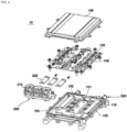
- FIG. 4 is an exploded perspective view of a converter according to an embodiment of the present invention
- FIG. 5 is a plan view illustrating an upper surface of a converter without a cover and a printed circuit board according to an embodiment of the present invention
- FIG. 6 is a plan view illustrating an upper surface of a converter without a cover according to an embodiment of the present invention
- FIG. 1 is a perspective view illustrating the outer appearance of a converter according to an embodiment of the present invention
- FIG. 2 is a plan view illustrating a lower surface of a converter according to an embodiment of the present invention
- FIG. 3 is a plan view illustrating an upper surface of a converter according to an embodiment of the present invention
- FIG. 7 is a plan view illustrating a lower surface of a printed circuit board according to an embodiment of the present invention
- FIG. 8 is a cross-sectional view of a heat dissipation structure in a converter according to an embodiment of the present invention
- FIG. 9 is a cross-sectional view taken along line A-A' of FIG. 3 .
- the outer appearance of the converter 10 may be formed by the housing 100.
- An internal space 101 may be formed inside the housing 100 so that components for driving the converter 10 are disposed.
- a cover 190 is coupled to an upper surface of the housing 100 and may cover the upper surface of the internal space 101. Screw holes are formed in the housing 100 and the cover 190 to allow screws to penetrate through regions corresponding to each other, and the housing 100 and the cover 190 can be screw-coupled together.
- a sealing member for sealing the internal space 101 may be disposed between the housing 100 and the cover 190.
- a connector module 200 may be disposed on a side surface of the housing 100.
- the connector module 200 is disposed on a side surface of the housing 100 and may be exposed to the outside. At least a portion of the connector module 200 is disposed inside the housing 100 and may be electrically connected to a printed circuit board 120, which will be described later.
- the connector module 200 electrically connects the converter 10 and a battery (not shown) and the converter 10 and a load, and power provided from the battery may be converted in the converter 10.
- the converted power may be applied to the load.
- the high voltage power applied from the battery may be converted in the converter 10 and a low voltage power may be applied to the load. Therefore, a configuration for applying a power to the converter 10 through the connector module 200 or a configuration for receiving a power from the converter 10 can be connected.
- the connector module 200 may be defined as including all configurations being disposed on an outer surface of the housing 10 in order to electrically and physically connect external terminals related to driving of the converter 10.
- the connector module 200 may include a bracket, a pin 210 being accommodated in the bracket, and a bus bar 220 electrically connecting the pin 210 and the printed circuit board 120.
- the converter 10 may include a refrigerant pipe 300.
- the refrigerant pipe 300 may be coupled to the housing 100.
- a heat dissipation space 110 may be formed inside the housing 100 to accommodate the refrigerant pipe 300. At least a portion of the refrigerant pipe 300 may be disposed inside the heat dissipation space 110 and the other portion is protruded outward from the heat dissipation space 110 to be exposed to the outside.
- a region where the heat dissipation space 110 is disposed may be protruded more downward than other regions.
- the arrangement region of the heat dissipation space 110 may be partitioned from other regions.
- the heat dissipation space 110 inside the housing 100 may have a partition wall shape surrounding the refrigerant pipe 300.
- the refrigerant pipe 300 has a flow path 301 so that the refrigerant flows therein, and a refrigerant inlet part 310 for introducing the refrigerant into the flow path 301 is disposed at one end, and the flow path 301 is disposed at the other end.
- the refrigerant pipe 300 may be formed in a pipe shape made of a metal material. Heat is exchanged by the refrigerant circulated along the flow path 301 so that the converter 10 can dissipate heat.
- the refrigerant pipe 300 and the housing 100 may be integrally formed by gravity casting.
- the refrigerant pipe 300 may include: a first straight portion 302 and a second straight portion 306 being disposed parallel to each other; and a connection portion 304 connecting the first straight portion 302 and the second straight portion 306.
- the connection portion 304 may be disposed perpendicular to the first straight portion 302 and the second straight portion 304.
- the connection region between the connection portion 304 and the first straight portion 302 and the connection region between the connection portion 304 and the second straight portion 306 may have a bent shape.
- the refrigerant inlet part 310 may be disposed at one end of the first straight portion 302, and the refrigerant discharge part 320 may be disposed at one end of the second straight portion 306.
- the partition wall of the heat dissipation space 110 is formed to surround the first straight portion 302, the second straight portion 306, and the connection portion 304 being disposed inside the housing 100; and the connection region between the first straight portion 302 and the connection portion 304, and the connection region between the second straight portion 306 and the connection portion 304 may be exposed to the space inside the housing 100.
- At least one electronic component for driving the converter 10 may be disposed in the internal space 101.
- the electronic component may include a printed circuit board 120, a first electronic component 122, and a second electronic component 130.
- the printed circuit board 120 is formed in a plate shape and may be disposed inside the internal space 101.
- An upper surface of the printed circuit board 120 is disposed to face the cover 190 and a lower surface of the printed circuit board 120 may be disposed to face a bottom surface of the internal space 101.
- a plurality of electronic components may be disposed on both surfaces of the printed circuit board 120.
- the first electronic component 122 is disposed on an upper surface of the printed circuit board 120, and the second electronic component 130 may be disposed on a lower surface of the printed circuit board 120.
- the first electronic component 122 may be disposed on an upper surface of the printed circuit board 120.
- the first electronic component 122 may include an FET device.
- the first electronic component 122 is provided in plurality and may be mounted on the printed circuit board 120.
- the plurality of first electronic components 122 may be disposed in a plurality of groups by forming a group of four.
- the four first electronic components 122 in a single group may be respectively disposed in corner regions. Each group may be spaced apart from each other.
- the first electronic component 122 may be disposed to be overlapped with the refrigerant pipe 300 in an up and down direction (first direction).
- the first electronic component 122 may be disposed to be overlapped with the first straight portion 302 and the second straight portion 306 in an up and down direction.
- the first electronic component 122 includes six groups, and the three groups overlap the first straight portion 302 in an up and down direction, and the remaining three groups may be disposed to be overlapped with the second straight portion 306 in an up and down direction.
- the lower surface of the printed circuit board 120 may be in contact with an outer surface of the heat dissipation space 110.
- a first heat conduction layer 129 may be disposed between the lower surface of the printed circuit board 120 and the upper surface of the heat dissipation space 110. Under the interposition of the first heat conduction layer 129, a lower surface of the printed circuit board 120 and an upper surface of the heat dissipation space 110 may be in contact with each other.
- the first heat conduction layer 129 is formed of a material having excellent thermal conductivity, and can transfer driving heat of the first electronic component 122 to the heat dissipation space 110.
- An upper surface of the heat dissipation space 110 on which the first heat conduction layer 129 is disposed may be a flat surface.
- the second electronic component 130 may be disposed on a lower surface of the printed circuit board 120.
- the second electronic component 130 may include an inductor for obtaining inductance.
- the second electronic component 130 is provided in plurality and may be mounted on a lower surface of the printed circuit board 120.
- Three of the second electronic components 130 forms one row and six of them may be disposed inside the internal space 101.
- the six of the second electronic components 130 may include: a first row being formed by a second-first electronic component 131, a second-second electronic component 132, and a second-third electronic component 133; and a second row being formed by a second-fourth electronic component 134, a second-fifth electronic component 135, and a second-sixth electronic component 136.
- Each of the second electronic components 130 may be disposed to be spaced apart from one another.
- a groove 102 to which the second electronic component 130 is coupled may be formed on a bottom surface of the internal space 101.
- the groove 102 is formed to correspond to the cross-sectional shape of the second electronic component 130, and a portion of the bottom surface of the internal space 101 may be recessed more downward than other regions.
- a portion of the second electronic component 130 may be accommodated inside the groove 102 and another portion thereof may be protruded outward from the groove 102.
- An upper region of the second electronic component 130 being protruded out of the groove 102 may be coupled to the printed circuit board 120.
- a protrusion 107 being protruded more downward than other regions may be disposed in a region corresponding to the region where the groove 102 is formed.
- the protrusion 107 may be disposed to be overlapped with a region of the heat dissipation space 110 protruded to a lower surface of the housing 100 in a horizontal direction.
- the second electronic component 130 may include a core and a coil being disposed inside the core.
- the core is disposed in the groove 102, and the coil is exposed upward of the core to be electrically connected to the printed circuit board 120.
- At least a portion of the second electronic component 130 is disposed to be overlapped with the refrigerant pipe 300 in a horizontal direction.
- the horizontal direction (second direction) may be understood as a direction perpendicular to an up and down direction and a direction parallel to the printed circuit board 120.
- the second-first electronic component 131, the second-second electronic component 132, and the second-third electronic component 133 may be disposed to be overlapped with the first straight portion 302 in a horizontal direction.
- the second-fourth electronic component 134, the second-fifth electronic component 135, and the second-sixth electronic component 136 may be disposed to be overlapped with the second straight portion 306 in a horizontal direction. Accordingly, driving heat of the second electronic component 130 can be easily transferred to the refrigerant pipe 300.
- a second heating layer 150 may be disposed between the inner surface of the groove 102 and the outer surface of the second electronic component 130.
- the second heat conduction layer 150 may include a side surface portion 152 being disposed between the side surface of the second electronic component 130 and the inner surface of the groove 102, and a lower surface portion 154 being disposed between the lower surface of the second electronic component 130 and the bottom surface of the groove 102.
- the cross section of the second heat conduction layer 150 may have the shape of a letter " ⁇ " by the side surface portion 152 and the lower surface portion 154.
- the second heat conduction layer 150 is formed of a material having excellent thermal conductivity, and can transfer driving heat of the second electronic component 130 to the refrigerant pipe 300 and the heat dissipation space 110.
- the second heat conduction layer 150 may have the shape of a pad.
- the first electronic component and the second electronic component being disposed on both sides of the printed circuit board form an optimal heat dissipation structure with the refrigerant pipe, there is an advantage in that heat dissipation efficiency can be enhanced.
Landscapes
- Engineering & Computer Science (AREA)
- Microelectronics & Electronic Packaging (AREA)
- Physics & Mathematics (AREA)
- Thermal Sciences (AREA)
- Power Engineering (AREA)
- Cooling Or The Like Of Electrical Apparatus (AREA)
- Dc-Dc Converters (AREA)
Abstract
Description
- The present embodiment relates to a converter.
- Engine electrical devices (starting devices, ignition devices, and charging devices) and lighting devices are common as automobile electrical devices, but recently, most systems, including chassis electrical devices, are becoming electrically electronic as vehicles become more electronically controlled.
- Various electrical components such as lamps, audio systems, heaters, and air conditioners installed in automobiles are designed to receive power from the battery when the car is stopped and from the generator when driving, and at this time, the generation capacity of the 14V power system is used as a normal power supply voltage.
- Recently, along with the development of the information technology industry, various new technologies (motor-type power steering, Internet, and the like) aimed to enhance the convenience of automobiles are being adopted by vehicles, and in the future, it is expected that the development of new technologies that can maximally utilize the current automotive systems will continue.
- A hybrid electric vehicle (HEV), regardless of soft or hard type, is equipped with a DC-DC converter (Low Voltage DC-DC Converter) for supplying an electric load (12V). In addition, the DC-DC converter, which serves as a generator (alternator) of a general gasoline vehicle, supplies a voltage of 12V for an electric load by lowering the high voltage of a main battery (usually a high-voltage battery of 144V or more).
- A DC-DC converter refers to an electronic circuit device that converts DC power of a certain voltage into DC power of another voltage, and is used in various fields such as television receivers and electrical components of automobiles.
- The outer appearance of the converter may be formed by the housing. One or more electronic components for driving are disposed inside the housing. As an example of the electronic component, there is a printed circuit board on which pluralities of elements are mounted. Elements being disposed on a printed circuit board generate heat by being driven. The generated heat may cause an overload of each electronic component, causing a trouble in a predetermined function and a failure. Accordingly, a structure or means for dissipating heat from components inside the converter is required.
- The present invention has been proposed to improve the above problems, and to provide a converter capable of improving heat dissipation efficiency by improving the structure.
- A converter according to the present embodiment comprises: a housing including an internal space; a printed circuit board being disposed inside the internal space; a first electronic component being disposed on an upper surface of the printed circuit board; a second electronic component disposed on a lower surface of the printed circuit board; and a heat dissipation space being disposed in the housing, wherein the first electronic component is disposed to be overlapped with the heat dissipation space in a first direction, and wherein the second electronic component is disposed to be overlapped with the heat dissipation space in a second direction perpendicular to the first direction.
- The first direction is an up and down direction, and the second direction may be a direction parallel to the printed circuit board.
- A first heat conduction layer may be disposed between an upper surface of the heat dissipation space and a lower surface of the printed circuit board.
- A groove being formed to be more recessed than other regions for accommodating the second electronic component may be disposed on a bottom surface of the internal space.
- A second heat conduction layer may be disposed between an inner surface of the groove and an outer surface of the second electronic component.
- The second heat conduction layer may include: a side surface portion being disposed between a side surface of the second electronic component and an inner surface of the groove; and a lower surface portion being disposed between the lower surface of the second electronic component and the bottom surface of the groove.
- It may include a refrigerant pipe being disposed inside the heat dissipation space and in which a refrigerant flows.
- The refrigerant pipe may comprise: a first straight portion having a refrigerant inlet part being disposed at one end; a second straight portion having a refrigerant discharge part being disposed at one end and parallel to the first straight portion; and a connection portion connecting the first straight portion and the second straight portion and perpendicular to the first straight portion and the second straight portion.
- The second electronic component may be provided in plurality, and some of them are disposed along a first row parallel to the first straight portion, and some of the remaining ones may be disposed along a second row parallel to the second straight portion.
- A converter according to another embodiment comprises: a printed circuit board; a first electronic component being disposed on an upper surface of the printed circuit board; a second electronic component being disposed on a lower surface of the printed circuit board; and a refrigerant pipe being disposed spaced apart from the lower surface of the printed circuit board, wherein the refrigerant pipe includes a first straight portion, a second straight portion parallel to the first straight portion, and a connection portion connecting the first straight portion and the second straight portion, wherein the first electronic component is disposed to be overlapped with the first straight portion, the second straight portion, and the connection portion in a direction perpendicular to the printed circuit board, and wherein the second electronic component is disposed between the first straight portion and the second straight portion.
- Through the present embodiment, since the first electronic component and the second electronic component being disposed on both surfaces of the printed circuit board form an optimal heat dissipation structure with the refrigerant pipe, there is an advantage in that heat dissipation efficiency can be enhanced.
- In particular, in the case of the second electronic component, since heat is dissipated not only from the lower surface but also from the side surface, there is an advantage in that the heat dissipation area of the electronic component can be increased.
-
-
FIG. 1 is a perspective view illustrating the outer appearance of a converter according to an embodiment of the present invention. -
FIG. 2 is a plan view illustrating a lower surface of a converter according to an embodiment of the present invention. -
FIG. 3 is a plan view illustrating an upper surface of a converter according to an embodiment of the present invention. -
FIG. 4 is an exploded perspective view of a converter according to an embodiment of the present invention. -
FIG. 5 is a plan view illustrating an upper surface of a converter without a cover and a printed circuit board according to an embodiment of the present invention. -
FIG. 6 is a plan view illustrating an upper surface of a converter without a cover according to an embodiment of the present invention. -
FIG. 7 is a plan view illustrating a lower surface of a printed circuit board according to an embodiment of the present invention. -
FIG. 8 is a cross-sectional view of a heat dissipation structure in a converter according to an embodiment of the present invention. -
FIG. 9 is a cross-sectional view taken along line A-A' ofFIG. 3 . - Hereinafter, preferred embodiments of the present invention will be described in detail with reference to the accompanying drawings.
- However, the technical idea of the present invention is not limited to some embodiments to be described, but may be implemented in various forms, and inside the scope of the technical idea of the present invention, one or more of the constituent elements may be selectively combined or substituted between embodiments.
- In addition, the terms (including technical and scientific terms) used in the embodiments of the present invention, unless explicitly defined and described, can be interpreted as a meaning that can be generally understood by a person skilled in the art, and commonly used terms such as terms defined in the dictionary may be interpreted in consideration of the meaning of the context of the related technology.
- In addition, terms used in the present specification are for describing embodiments and are not intended to limit the present invention.
- In the present specification, the singular form may include the plural form unless specifically stated in the phrase, and when described as "at least one (or more than one) of A and B and C", it may include one or more of all combinations that can be combined with A, B, and C.
- In addition, in describing the components of the embodiment of the present invention, terms such as first, second, A, B, (a), and (b) may be used. These terms are merely intended to distinguish the components from other components, and the terms do not limit the nature, order or sequence of the components.
- And, when a component is described as being 'connected', 'coupled' or 'interconnected' to another component, the component is not only directly connected, coupled or interconnected to the other component, but may also include cases of being 'connected', 'coupled', or 'interconnected' due that another component between that other components.
- In addition, when described as being formed or arranged in "on (above)" or "below (under)" of each component, "on (above)" or "below (under)" means that it includes not only the case where the two components are directly in contact with, but also the case where one or more other components are formed or arranged between the two components. In addition, when expressed as "on (above)" or "below (under)", the meaning of not only an upward direction but also a downward direction based on one component may be included.
-
FIG. 1 is a perspective view illustrating the outer appearance of a converter according to an embodiment of the present invention;FIG. 2 is a plan view illustrating a lower surface of a converter according to an embodiment of the present invention;FIG. 3 is a plan view illustrating an upper surface of a converter according to an embodiment of the present invention;FIG. 4 is an exploded perspective view of a converter according to an embodiment of the present invention;FIG. 5 is a plan view illustrating an upper surface of a converter without a cover and a printed circuit board according to an embodiment of the present invention;FIG. 6 is a plan view illustrating an upper surface of a converter without a cover according to an embodiment of the present invention;FIG. 7 is a plan view illustrating a lower surface of a printed circuit board according to an embodiment of the present invention;FIG. 8 is a cross-sectional view of a heat dissipation structure in a converter according to an embodiment of the present invention; andFIG. 9 is a cross-sectional view taken along line A-A' ofFIG. 3 . - Referring to
FIGS. 1 to 9 , the outer appearance of theconverter 10 according to an embodiment of the present invention may be formed by thehousing 100. Aninternal space 101 may be formed inside thehousing 100 so that components for driving theconverter 10 are disposed. Acover 190 is coupled to an upper surface of thehousing 100 and may cover the upper surface of theinternal space 101. Screw holes are formed in thehousing 100 and thecover 190 to allow screws to penetrate through regions corresponding to each other, and thehousing 100 and thecover 190 can be screw-coupled together. A sealing member for sealing theinternal space 101 may be disposed between thehousing 100 and thecover 190. - A
connector module 200 may be disposed on a side surface of thehousing 100. Theconnector module 200 is disposed on a side surface of thehousing 100 and may be exposed to the outside. At least a portion of theconnector module 200 is disposed inside thehousing 100 and may be electrically connected to a printedcircuit board 120, which will be described later. - The
connector module 200 electrically connects theconverter 10 and a battery (not shown) and theconverter 10 and a load, and power provided from the battery may be converted in theconverter 10. The converted power may be applied to the load. For example, the high voltage power applied from the battery may be converted in theconverter 10 and a low voltage power may be applied to the load. Therefore, a configuration for applying a power to theconverter 10 through theconnector module 200 or a configuration for receiving a power from theconverter 10 can be connected. - However, this is exemplary, and the
connector module 200 may be defined as including all configurations being disposed on an outer surface of thehousing 10 in order to electrically and physically connect external terminals related to driving of theconverter 10. - The
connector module 200 may include a bracket, apin 210 being accommodated in the bracket, and abus bar 220 electrically connecting thepin 210 and the printedcircuit board 120. - The
converter 10 may include arefrigerant pipe 300. Therefrigerant pipe 300 may be coupled to thehousing 100. Aheat dissipation space 110 may be formed inside thehousing 100 to accommodate therefrigerant pipe 300. At least a portion of therefrigerant pipe 300 may be disposed inside theheat dissipation space 110 and the other portion is protruded outward from theheat dissipation space 110 to be exposed to the outside. Among the lower surfaces of thehousing 100, a region where theheat dissipation space 110 is disposed may be protruded more downward than other regions. Among the spaces inside thehousing 100, the arrangement region of theheat dissipation space 110 may be partitioned from other regions. For example, theheat dissipation space 110 inside thehousing 100 may have a partition wall shape surrounding therefrigerant pipe 300. - The
refrigerant pipe 300 has aflow path 301 so that the refrigerant flows therein, and arefrigerant inlet part 310 for introducing the refrigerant into theflow path 301 is disposed at one end, and theflow path 301 is disposed at the other end. Arefrigerant discharge part 320 through which the refrigerant that has been circulated is discharged is disposed. Therefrigerant pipe 300 may be formed in a pipe shape made of a metal material. Heat is exchanged by the refrigerant circulated along theflow path 301 so that theconverter 10 can dissipate heat. - The
refrigerant pipe 300 and thehousing 100 may be integrally formed by gravity casting. - The
refrigerant pipe 300 may include: a firststraight portion 302 and a secondstraight portion 306 being disposed parallel to each other; and aconnection portion 304 connecting the firststraight portion 302 and the secondstraight portion 306. Theconnection portion 304 may be disposed perpendicular to the firststraight portion 302 and the secondstraight portion 304. The connection region between theconnection portion 304 and the firststraight portion 302 and the connection region between theconnection portion 304 and the secondstraight portion 306 may have a bent shape. Therefrigerant inlet part 310 may be disposed at one end of the firststraight portion 302, and therefrigerant discharge part 320 may be disposed at one end of the secondstraight portion 306. - The partition wall of the
heat dissipation space 110 is formed to surround the firststraight portion 302, the secondstraight portion 306, and theconnection portion 304 being disposed inside thehousing 100; and the connection region between the firststraight portion 302 and theconnection portion 304, and the connection region between the secondstraight portion 306 and theconnection portion 304 may be exposed to the space inside thehousing 100. - At least one electronic component for driving the
converter 10 may be disposed in theinternal space 101. The electronic component may include a printedcircuit board 120, a firstelectronic component 122, and a secondelectronic component 130. - The printed
circuit board 120 is formed in a plate shape and may be disposed inside theinternal space 101. An upper surface of the printedcircuit board 120 is disposed to face thecover 190 and a lower surface of the printedcircuit board 120 may be disposed to face a bottom surface of theinternal space 101. A plurality of electronic components may be disposed on both surfaces of the printedcircuit board 120. The firstelectronic component 122 is disposed on an upper surface of the printedcircuit board 120, and the secondelectronic component 130 may be disposed on a lower surface of the printedcircuit board 120. - The first
electronic component 122 may be disposed on an upper surface of the printedcircuit board 120. The firstelectronic component 122 may include an FET device. The firstelectronic component 122 is provided in plurality and may be mounted on the printedcircuit board 120. The plurality of firstelectronic components 122 may be disposed in a plurality of groups by forming a group of four. The four firstelectronic components 122 in a single group may be respectively disposed in corner regions. Each group may be spaced apart from each other. - The first
electronic component 122 may be disposed to be overlapped with therefrigerant pipe 300 in an up and down direction (first direction). The firstelectronic component 122 may be disposed to be overlapped with the firststraight portion 302 and the secondstraight portion 306 in an up and down direction. For example, the firstelectronic component 122 includes six groups, and the three groups overlap the firststraight portion 302 in an up and down direction, and the remaining three groups may be disposed to be overlapped with the secondstraight portion 306 in an up and down direction. - The lower surface of the printed
circuit board 120 may be in contact with an outer surface of theheat dissipation space 110. A firstheat conduction layer 129 may be disposed between the lower surface of the printedcircuit board 120 and the upper surface of theheat dissipation space 110. Under the interposition of the firstheat conduction layer 129, a lower surface of the printedcircuit board 120 and an upper surface of theheat dissipation space 110 may be in contact with each other. The firstheat conduction layer 129 is formed of a material having excellent thermal conductivity, and can transfer driving heat of the firstelectronic component 122 to theheat dissipation space 110. An upper surface of theheat dissipation space 110 on which the firstheat conduction layer 129 is disposed may be a flat surface. - The second
electronic component 130 may be disposed on a lower surface of the printedcircuit board 120. The secondelectronic component 130 may include an inductor for obtaining inductance. The secondelectronic component 130 is provided in plurality and may be mounted on a lower surface of the printedcircuit board 120. Three of the secondelectronic components 130 forms one row and six of them may be disposed inside theinternal space 101. The six of the secondelectronic components 130 may include: a first row being formed by a second-firstelectronic component 131, a second-secondelectronic component 132, and a second-thirdelectronic component 133; and a second row being formed by a second-fourthelectronic component 134, a second-fifthelectronic component 135, and a second-sixthelectronic component 136. Each of the secondelectronic components 130 may be disposed to be spaced apart from one another. - A
groove 102 to which the secondelectronic component 130 is coupled may be formed on a bottom surface of theinternal space 101. Thegroove 102 is formed to correspond to the cross-sectional shape of the secondelectronic component 130, and a portion of the bottom surface of theinternal space 101 may be recessed more downward than other regions. A portion of the secondelectronic component 130 may be accommodated inside thegroove 102 and another portion thereof may be protruded outward from thegroove 102. An upper region of the secondelectronic component 130 being protruded out of thegroove 102 may be coupled to the printedcircuit board 120. Of the lower surface of thehousing 100, a protrusion 107 being protruded more downward than other regions may be disposed in a region corresponding to the region where thegroove 102 is formed. The protrusion 107 may be disposed to be overlapped with a region of theheat dissipation space 110 protruded to a lower surface of thehousing 100 in a horizontal direction. - The second
electronic component 130 may include a core and a coil being disposed inside the core. The core is disposed in thegroove 102, and the coil is exposed upward of the core to be electrically connected to the printedcircuit board 120. - At least a portion of the second
electronic component 130 is disposed to be overlapped with therefrigerant pipe 300 in a horizontal direction. The horizontal direction (second direction) may be understood as a direction perpendicular to an up and down direction and a direction parallel to the printedcircuit board 120. The second-firstelectronic component 131, the second-secondelectronic component 132, and the second-thirdelectronic component 133 may be disposed to be overlapped with the firststraight portion 302 in a horizontal direction. The second-fourthelectronic component 134, the second-fifthelectronic component 135, and the second-sixthelectronic component 136 may be disposed to be overlapped with the secondstraight portion 306 in a horizontal direction. Accordingly, driving heat of the secondelectronic component 130 can be easily transferred to therefrigerant pipe 300. - Meanwhile, a
second heating layer 150 may be disposed between the inner surface of thegroove 102 and the outer surface of the secondelectronic component 130. The secondheat conduction layer 150 may include aside surface portion 152 being disposed between the side surface of the secondelectronic component 130 and the inner surface of thegroove 102, and alower surface portion 154 being disposed between the lower surface of the secondelectronic component 130 and the bottom surface of thegroove 102. The cross section of the secondheat conduction layer 150 may have the shape of a letter "⊏" by theside surface portion 152 and thelower surface portion 154. The secondheat conduction layer 150 is formed of a material having excellent thermal conductivity, and can transfer driving heat of the secondelectronic component 130 to therefrigerant pipe 300 and theheat dissipation space 110. The secondheat conduction layer 150 may have the shape of a pad. - According to the structure as described above, since the first electronic component and the second electronic component being disposed on both sides of the printed circuit board form an optimal heat dissipation structure with the refrigerant pipe, there is an advantage in that heat dissipation efficiency can be enhanced.
- In particular, in the case of the second electronic component, since heat is dissipated not only from the lower surface but also from the side surface, there is an advantage in that the heat dissipation area of the electronic component can be increased.
- In the above description, it is described that all the components constituting the embodiments of the present invention are combined or operated in one, but the present invention is not necessarily limited to these embodiments. In other words, within the scope of the present invention, all of the components may be selectively operated in combination with one or more. In addition, the terms "comprise", "include" or "having" described above mean that the corresponding component may be inherent unless specifically stated otherwise, and thus it should be construed that it does not exclude other components, but further include other components instead. All terms, including technical and scientific terms, have the same meaning as commonly understood by one of ordinary skill in the art unless otherwise defined. Terms used generally, such as terms defined in a dictionary, should be interpreted to coincide with the contextual meaning of the related art, and shall not be interpreted in an ideal or excessively formal sense unless explicitly defined in the present invention.
- The above description is merely illustrative of the technical idea of the present invention, and those skilled in the art to which the present invention pertains may make various modifications and changes without departing from the essential characteristics of the present invention. Therefore, the embodiments disclosed in the present invention are not intended to limit the technical idea of the present invention but to describe the present invention, and the scope of the technical idea of the present invention is not limited by these embodiments. The protection scope of the present invention should be interpreted by the following claims, and all technical ideas within the equivalent scope should be interpreted as being included in the scope of the present invention.
Claims (10)
- A converter comprising:a housing including an internal space;a printed circuit board being disposed inside the internal space;a first electronic component being disposed on an upper surface of the printed circuit board;a second electronic component disposed on a lower surface of the printed circuit board; anda heat dissipation space being disposed in the housing,wherein the first electronic component is disposed to be overlapped with the heat dissipation space in a first direction, andwherein the second electronic component is disposed to be overlapped with the heat dissipation space in a second direction perpendicular to the first direction.
- The converter according to claim 1,wherein the first direction is an up and down direction, andwherein the second direction is a direction parallel to the printed circuit board.
- The converter according to claim 1,
wherein a first heat conduction layer is disposed between an upper surface of the - The converter according to any one claim among claims 1 to 3,
wherein a groove being formed to be more recessed than other regions and accommodating the second electronic component is disposed on a bottom surface of the internal space. - The converter according to claim 4,
wherein a second heat conduction layer is disposed between an inner surface of the groove and an outer surface of the second electronic component. - The converter according to claim 5,
wherein the second heat conduction layer include a side surface portion being disposed between a side surface of the second electronic component and an inner surface of the groove, and a lower surface portion being disposed between the lower surface of the second electronic component and the bottom surface of the groove - The converter according to any one claim among claims 1 to 3, including:
a refrigerant pipe being disposed inside the heat dissipation space and in which a refrigerant flows - The converter according to claim 7
wherein the refrigerant pipe comprises a first straight portion having a refrigerant inlet part being disposed at one end, a second straight portion having a refrigerant discharge part being disposed at one end and parallel to the first straight portion, and a connection portion connecting the first straight portion and the second straight portion and perpendicular to the first straight portion and the second straight portion. - The converter according to claim 8,
wherein the second electronic component is provided in plurality and some of them are disposed along a first row parallel to the first straight portion, and some of the remaining ones are disposed along a second row parallel to the second straight portion. - A converter comprising:a printed circuit board;a first electronic component being disposed on an upper surface of the printed circuit board;a second electronic component being disposed on a lower surface of the printed circuit board; anda refrigerant pipe being disposed spaced apart from the lower surface of the printed circuit board,wherein the refrigerant pipe includes a first straight portion, a second straight portion parallel to the first straight portion, and a connection portion connecting the first straight portion and the second straight portion,wherein the first electronic component is disposed to be overlapped with the first straight portion, the second straight portion, and the connection portion in a direction perpendicular to the printed circuit board, andwherein the second electronic component is disposed between the first straight portion and the second straight portion.
Applications Claiming Priority (2)
| Application Number | Priority Date | Filing Date | Title |
|---|---|---|---|
| KR1020210001038A KR20220099022A (en) | 2021-01-05 | 2021-01-05 | Converter |
| PCT/KR2022/000107 WO2022149834A1 (en) | 2021-01-05 | 2022-01-04 | Converter |
Publications (2)
| Publication Number | Publication Date |
|---|---|
| EP4277444A1 true EP4277444A1 (en) | 2023-11-15 |
| EP4277444A4 EP4277444A4 (en) | 2024-12-18 |
Family
ID=82358189
Family Applications (1)
| Application Number | Title | Priority Date | Filing Date |
|---|---|---|---|
| EP22736811.5A Pending EP4277444A4 (en) | 2021-01-05 | 2022-01-04 | CONVERTER |
Country Status (6)
| Country | Link |
|---|---|
| US (1) | US20240324153A1 (en) |
| EP (1) | EP4277444A4 (en) |
| JP (1) | JP7840336B2 (en) |
| KR (1) | KR20220099022A (en) |
| CN (1) | CN116724486A (en) |
| WO (1) | WO2022149834A1 (en) |
Families Citing this family (1)
| Publication number | Priority date | Publication date | Assignee | Title |
|---|---|---|---|---|
| US20240305094A1 (en) * | 2023-03-06 | 2024-09-12 | Vanair Manufacturing, Inc. | Jump starter |
Family Cites Families (10)
| Publication number | Priority date | Publication date | Assignee | Title |
|---|---|---|---|---|
| JP5407275B2 (en) * | 2008-10-27 | 2014-02-05 | 株式会社デンソー | Power converter |
| JP5262752B2 (en) * | 2009-01-26 | 2013-08-14 | 株式会社デンソー | Power converter |
| JP5644628B2 (en) * | 2011-03-29 | 2014-12-24 | 株式会社デンソー | Switching power supply |
| WO2013080317A1 (en) * | 2011-11-30 | 2013-06-06 | 三菱電機株式会社 | Semiconductor device, and on-board power conversion device |
| EP2830073B1 (en) * | 2012-03-19 | 2017-09-13 | Mitsubishi Electric Corporation | Power conversion apparatus |
| RU2496134C1 (en) * | 2012-07-02 | 2013-10-20 | Сергей Михайлович Абрамов | Server farm with immersion cooling system |
| JP5783212B2 (en) | 2013-09-06 | 2015-09-24 | Tdk株式会社 | Power supply |
| US9913404B2 (en) | 2014-06-24 | 2018-03-06 | Mitsubishi Electric Corporation | Cooling apparatus |
| JP2018186143A (en) | 2017-04-25 | 2018-11-22 | オムロンオートモーティブエレクトロニクス株式会社 | Circuit board module, electronic device |
| JP2020198347A (en) * | 2019-05-31 | 2020-12-10 | 株式会社豊田自動織機 | Power conversion apparatus |
-
2021
- 2021-01-05 KR KR1020210001038A patent/KR20220099022A/en active Pending
-
2022
- 2022-01-04 WO PCT/KR2022/000107 patent/WO2022149834A1/en not_active Ceased
- 2022-01-04 JP JP2023540937A patent/JP7840336B2/en active Active
- 2022-01-04 CN CN202280008773.7A patent/CN116724486A/en active Pending
- 2022-01-04 US US18/259,737 patent/US20240324153A1/en active Pending
- 2022-01-04 EP EP22736811.5A patent/EP4277444A4/en active Pending
Also Published As
| Publication number | Publication date |
|---|---|
| US20240324153A1 (en) | 2024-09-26 |
| JP7840336B2 (en) | 2026-04-03 |
| KR20220099022A (en) | 2022-07-12 |
| JP2024501776A (en) | 2024-01-15 |
| EP4277444A4 (en) | 2024-12-18 |
| WO2022149834A1 (en) | 2022-07-14 |
| CN116724486A (en) | 2023-09-08 |
Similar Documents
| Publication | Publication Date | Title |
|---|---|---|
| EP3606306B1 (en) | Converter | |
| US20250030336A1 (en) | Multi-pipe converter | |
| KR102458346B1 (en) | Converter | |
| EP4277444A1 (en) | Converter | |
| US20240396468A1 (en) | Converter | |
| KR102590523B1 (en) | Converter | |
| CN114982392B (en) | Converter | |
| EP3866574B1 (en) | Electronic component assembly | |
| KR102515174B1 (en) | Power terminal module | |
| KR20220157198A (en) | Converter | |
| EP4436022A1 (en) | Converter | |
| JP7814282B2 (en) | Power Conversion Device | |
| KR102631926B1 (en) | Converter | |
| KR102645803B1 (en) | Converter | |
| KR102653879B1 (en) | Converter | |
| JP2013022991A (en) | In-vehicle power supply device | |
| KR20200008905A (en) | Connector module and Converter having the same | |
| KR20190059635A (en) | Converter | |
| EP3905867A1 (en) | Power conversion device | |
| KR20230073100A (en) | Converter | |
| CN118285050A (en) | converter | |
| KR20210039580A (en) | Circuit board module and Converter having the same | |
| KR20190143180A (en) | Converter |
Legal Events
| Date | Code | Title | Description |
|---|---|---|---|
| STAA | Information on the status of an ep patent application or granted ep patent |
Free format text: STATUS: THE INTERNATIONAL PUBLICATION HAS BEEN MADE |
|
| PUAI | Public reference made under article 153(3) epc to a published international application that has entered the european phase |
Free format text: ORIGINAL CODE: 0009012 |
|
| STAA | Information on the status of an ep patent application or granted ep patent |
Free format text: STATUS: REQUEST FOR EXAMINATION WAS MADE |
|
| 17P | Request for examination filed |
Effective date: 20230627 |
|
| AK | Designated contracting states |
Kind code of ref document: A1 Designated state(s): AL AT BE BG CH CY CZ DE DK EE ES FI FR GB GR HR HU IE IS IT LI LT LU LV MC MK MT NL NO PL PT RO RS SE SI SK SM TR |
|
| DAV | Request for validation of the european patent (deleted) | ||
| DAX | Request for extension of the european patent (deleted) | ||
| A4 | Supplementary search report drawn up and despatched |
Effective date: 20241114 |
|
| RIC1 | Information provided on ipc code assigned before grant |
Ipc: H02M 7/00 20060101ALI20241108BHEP Ipc: H05K 7/20 20060101AFI20241108BHEP |