EP4266499B1 - Multiband antenna - Google Patents
Multiband antenna Download PDFInfo
- Publication number
- EP4266499B1 EP4266499B1 EP23165262.9A EP23165262A EP4266499B1 EP 4266499 B1 EP4266499 B1 EP 4266499B1 EP 23165262 A EP23165262 A EP 23165262A EP 4266499 B1 EP4266499 B1 EP 4266499B1
- Authority
- EP
- European Patent Office
- Prior art keywords
- multiband antenna
- edge portion
- slot edge
- slot
- radiation element
- Prior art date
- Legal status (The legal status is an assumption and is not a legal conclusion. Google has not performed a legal analysis and makes no representation as to the accuracy of the status listed.)
- Active
Links
Images




Classifications
-
- H—ELECTRICITY
- H01—ELECTRIC ELEMENTS
- H01Q—ANTENNAS, i.e. RADIO AERIALS
- H01Q13/00—Waveguide horns or mouths; Slot antennas; Leaky-waveguide antennas; Equivalent structures causing radiation along the transmission path of a guided wave
- H01Q13/10—Resonant slot antennas
- H01Q13/103—Resonant slot antennas with variable reactance for tuning the antenna
-
- H—ELECTRICITY
- H01—ELECTRIC ELEMENTS
- H01Q—ANTENNAS, i.e. RADIO AERIALS
- H01Q5/00—Arrangements for simultaneous operation of antennas on two or more different wavebands, e.g. dual-band or multi-band arrangements
- H01Q5/30—Arrangements for providing operation on different wavebands
- H01Q5/307—Individual or coupled radiating elements, each element being fed in an unspecified way
- H01Q5/342—Individual or coupled radiating elements, each element being fed in an unspecified way for different propagation modes
- H01Q5/357—Individual or coupled radiating elements, each element being fed in an unspecified way for different propagation modes using a single feed point
- H01Q5/364—Creating multiple current paths
- H01Q5/371—Branching current paths
-
- H—ELECTRICITY
- H01—ELECTRIC ELEMENTS
- H01Q—ANTENNAS, i.e. RADIO AERIALS
- H01Q5/00—Arrangements for simultaneous operation of antennas on two or more different wavebands, e.g. dual-band or multi-band arrangements
- H01Q5/30—Arrangements for providing operation on different wavebands
- H01Q5/307—Individual or coupled radiating elements, each element being fed in an unspecified way
-
- H—ELECTRICITY
- H01—ELECTRIC ELEMENTS
- H01Q—ANTENNAS, i.e. RADIO AERIALS
- H01Q1/00—Details of, or arrangements associated with, antennas
- H01Q1/48—Earthing means; Earth screens; Counterpoises
-
- H—ELECTRICITY
- H01—ELECTRIC ELEMENTS
- H01Q—ANTENNAS, i.e. RADIO AERIALS
- H01Q1/00—Details of, or arrangements associated with, antennas
- H01Q1/50—Structural association of antennas with earthing switches, lead-in devices or lightning protectors
-
- H—ELECTRICITY
- H01—ELECTRIC ELEMENTS
- H01Q—ANTENNAS, i.e. RADIO AERIALS
- H01Q13/00—Waveguide horns or mouths; Slot antennas; Leaky-waveguide antennas; Equivalent structures causing radiation along the transmission path of a guided wave
- H01Q13/10—Resonant slot antennas
-
- H—ELECTRICITY
- H01—ELECTRIC ELEMENTS
- H01Q—ANTENNAS, i.e. RADIO AERIALS
- H01Q13/00—Waveguide horns or mouths; Slot antennas; Leaky-waveguide antennas; Equivalent structures causing radiation along the transmission path of a guided wave
- H01Q13/10—Resonant slot antennas
- H01Q13/106—Microstrip slot antennas
-
- H—ELECTRICITY
- H01—ELECTRIC ELEMENTS
- H01Q—ANTENNAS, i.e. RADIO AERIALS
- H01Q5/00—Arrangements for simultaneous operation of antennas on two or more different wavebands, e.g. dual-band or multi-band arrangements
- H01Q5/10—Resonant antennas
-
- H—ELECTRICITY
- H01—ELECTRIC ELEMENTS
- H01Q—ANTENNAS, i.e. RADIO AERIALS
- H01Q5/00—Arrangements for simultaneous operation of antennas on two or more different wavebands, e.g. dual-band or multi-band arrangements
- H01Q5/20—Arrangements for simultaneous operation of antennas on two or more different wavebands, e.g. dual-band or multi-band arrangements characterised by the operating wavebands
- H01Q5/28—Arrangements for establishing polarisation or beam width over two or more different wavebands
-
- H—ELECTRICITY
- H01—ELECTRIC ELEMENTS
- H01Q—ANTENNAS, i.e. RADIO AERIALS
- H01Q5/00—Arrangements for simultaneous operation of antennas on two or more different wavebands, e.g. dual-band or multi-band arrangements
- H01Q5/50—Feeding or matching arrangements for broad-band or multi-band operation
-
- H—ELECTRICITY
- H01—ELECTRIC ELEMENTS
- H01Q—ANTENNAS, i.e. RADIO AERIALS
- H01Q9/00—Electrically-short antennas having dimensions not more than twice the operating wavelength and consisting of conductive active radiating elements
- H01Q9/04—Resonant antennas
- H01Q9/0407—Substantially flat resonant element parallel to ground plane, e.g. patch antenna
- H01Q9/0421—Substantially flat resonant element parallel to ground plane, e.g. patch antenna with a shorting wall or a shorting pin at one end of the element
-
- H—ELECTRICITY
- H01—ELECTRIC ELEMENTS
- H01Q—ANTENNAS, i.e. RADIO AERIALS
- H01Q9/00—Electrically-short antennas having dimensions not more than twice the operating wavelength and consisting of conductive active radiating elements
- H01Q9/04—Resonant antennas
- H01Q9/30—Resonant antennas with feed to end of elongated active element, e.g. unipole
- H01Q9/42—Resonant antennas with feed to end of elongated active element, e.g. unipole with folded element, the folded parts being spaced apart a small fraction of the operating wavelength
Definitions
- This invention relates to a multiband antenna, particularly, to a multiband antenna provided with a slot antenna and a radiation element.
- US 2021/126373 A1 discloses an antenna comprising a split ring resonator.
- the antenna has a main portion, a feeding portion and at least one radiation element.
- the main portion forms a split ring.
- the feeding portion is provided on the main portion.
- the radiation element extends from the main portion.
- CN 102 790 262 A discloses an antenna and an electronic device with the antenna.
- the antenna comprises a grounding part, a main radiation part and a shield wall, wherein the main radiation part comprises a first radiation part and a second radiation part which are in symmetrical structures, wherein the first radiation part comprises a first feed-in end; the second radiation part comprises a second feed-in end; the main radiation part and the shield wall are respectively connected to the two sides of the grounding part and are opposite to each other.
- the antenna has two feed-in ends in two different directions, so as to select two coaxial arrangement manners.
- a multiband antenna 90 disclosed in JP 2021-136527A Patent Document 1 is provided with a slot antenna 92 and a radiation element 94.
- a slot 921 of the slot antenna 92 has a longitudinal direction in a first direction or a Y-direction.
- the radiation element 94 has a first part 941 and a second part 943.
- the first part 941 extends from the slot antenna 92 in a second direction or an X-direction perpendicular to the first direction.
- the second part 943 extends from an end portion of the first part 941 in the first direction.
- the second part 943 is larger than the first part 941 in length.
- the multiband antenna 90 of Patent Document 1 has two resonant frequencies or operating frequencies, namely, a resonant frequency of the slot antenna 92 and a resonant frequency of the radiation element 94.
- the second part 943 of the radiation element 94 extends in the first direction and lowers the resonant frequency of the slot antenna 92 in comparison with a case where the radiation element 94 is not provided. This means that the use of the radiation element 94 can cause downsizing of the slot antenna 90 which has a specific resonant frequency.
- the object is achieved by the multiband antenna according to claim 1.
- the additional element adjusts an impedance of the multiband antenna, and thereby a resonant frequency of the slot antenna can be lowered.
- the additional element can downsize the slot antenna having a specific resonant frequency, so that the multiband antenna can be downsized.
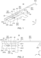
- a multiband antenna 10 according to an embodiment of the present invention is provided with a conductive main portion 20, a first radiation element (radiation element) 30 and an additional element 40.
- the multiband antenna 10 is further provided with a second radiation element (additional radiation element) 50 and a grounding terminal 60.
- the second radiation element 50 and the grounding terminal 60 are not essential. Nevertheless, by providing the second radiation element 50, a bandwidth of the multiband antenna 10 can be widened.
- the multiband antenna 10 is formed of a single sheet metal.
- the multiband antenna 10 is formed by punching and bending a single metal sheet.
- the present invention is not limited thereto.
- the multiband antenna 10 may be formed of a plurality of metal sheets.
- the multiband antenna 10 may be formed of a metal foil or a conductive pattern formed on a circuit board instead of the metal sheet at least in part.
- the multiband antenna 10 may be formed of a metal sheet or a metal foil and a supporter which is made of resin and supports the metal sheet or the metal foil if necessary.
- the conductive main portion 20 has at least a first slot edge portion 201 and a second slot edge portion 203.
- the conductive main portion 20 further has a coupling portion 205.
- the first slot edge portion 201, the second slot edge portion 203 and the coupling portion 205 are coupled to one another and define a slot 22 and an open portion 24.
- the conductive main portion 20 is formed with the slot 22 and the open portion 24.
- the conductive main portion 20 is located on a specific plane defined by a first direction and a second direction perpendicular to the first direction.
- the first direction is a Y-direction
- the second direction is an X-direction.
- the specific plane is an X-Y plane.
- the first direction defines a first orientation and a second orientation which is an orientation opposite to the first orientation.
- the first orientation is a negative Y-direction
- the second orientation is a positive Y-direction.
- the second direction is also a front-rear direction. A negative X-direction is directed forward while a positive X-direction is directed rearward.
- each of the first slot edge portion 201 and the second slot edge portion 203 has a rectangular shape long in a first direction.
- the first slot edge portion 201 has an end portion 2011, which is oriented in the first orientation of the first direction, and an end portion 2013, which is oriented in the second orientation of the first direction.
- the second slot edge portion 203 has an end portion 2031, which is oriented in the first orientation of the first direction, and an end portion 2033, which is oriented in the second orientation of the first direction.
- the first slot edge portion 201 and the second slot edge portion 203 are positioned apart from each other in the second direction.
- the first slot edge portion 201 is located forward of the second slot edge portion 203.
- the slot 22 and the open portion 24 are located between the first slot edge portion 201 and the second slot edge portion 203.
- the first slot edge portion 201 and the second slot edge portion 203 are arranged so that they sandwich the slot 22 and the open portion 24 therebetween.
- the coupling portion 205 has a rectangular shape long in the second direction.
- the coupling portion 205 couples one of the end portions of the first slot edge portion 201 to one of the end portions of the second slot edge portion 203.
- the coupling portion 205 couples the end portion 2013 of the first slot edge portion 201 and the end portion 2033 of the second slot edge portion 203 to each other.
- the slot 22 has a longitudinal direction in the first direction.
- the open portion 24 is located at an end portion of the conductive main portion 20, wherein the end portion of the conductive main portion 20 is oriented in the first orientation.
- the open portion 24 is located between the end portion 2011 of the first slot edge portion 201 and the end portion 2031 of the second slot edge portion 203.
- the open portion 24 is contiguous to the slot 22 and opens the slot 22 outside of the conductive main portion 20.
- the open portion 24 is opened in the first orientation of the first direction.
- the open portion 24 may be opened forward or rearward. Even when the open portion 24 is opened forward or rearward, the open portion 24 of the present invention is formed at a part of the conductive main portion 20 which is different from the first slot edge portion 201.
- the first radiation element 30 has a first part 301 and a second part 303.
- the first part 301 has a rectangular shape long in the second direction and is located on a specific plane.
- the first part 301 extends in the second direction from the end portion 2011 of the first slot edge portion 201, wherein the end portion 2011 is oriented in the first orientation of the first direction.
- the first part 301 extends rearward.
- the second part 303 of the first radiation element 30 extends from a rear end portion of the first part 301 in the second orientation of the first direction.
- the second part 303 has an upper portion 321 and a rear portion 323.
- the upper portion 321 has a rectangular shape long in the first direction and is located on the specific plane.
- the rear portion 323 has a rectangular shape long in the first direction and extends from a rear edge of the upper portion 321 in a third direction perpendicular to both the first direction and the second direction.
- the rear portion 323 is not essential. However, the rear portion 323 can increase a radiation efficiency of the first radiation element 30 without increasing an occupation area of the first radiation element 30 when viewed along the third direction.
- the third direction is a Z-direction. Supposing a positive Z-direction is directed upward while a negative Z-direction is directed downward, the rear portion 323 extends downward from the upper portion 321.
- the additional element 40 extends forward from a lower edge of the rear portion 323 of the second part 303 of the first radiation element 30.
- the additional element 40 is positioned apart from the conductive main portion 20 in the third direction and extends forward without being brought into contact with the conductive main portion 20.
- the additional element 40 has a rectangular shape.
- the additional element 40 is positioned apart from both ends of the second part 303 in the first direction.
- the additional element 40 is nearer to an end portion of the second part 303, which is oriented in the second orientation, than to an end portion of the second part 303, which is oriented in the first orientation, in the first direction.
- the present invention is not limited thereto.
- the shape and the position of the additional element 40 may be freely set according to intended antenna properties.
- the additional element 40 extends toward a second specific area 75 through a first specific area 70.
- the additional element 40 extends to the second specific area 75.
- the additional element 40 overlaps with the second slot edge portion 203 when viewed along the third direction.
- each of the first specific area 70 and the second specific area 75 is an area on a plane which is perpendicular to the third direction and which is positioned apart from the specific plane in the third direction.
- the first specific area 70 is an area overlapping with the first slot edge portion 201 in the third direction.
- the second specific area 75 is an area overlapping with the second slot edge portion 203 in the third direction.
- the additional element 40 is located on a plane in which the first specific area 70 and the second specific area 75 are included, and a front edge 401 of the additional element 40 is in the second specific area 75.
- the present invention is not limited thereto.
- Each of the first specific area 70 and the second specific area 75 may be freely set according to intended antenna properties.
- the front edge 401 of the additional element 40 is located near to the second slot edge portion 203.
- a capacitor is formed between the additional element 40 and the second slot edge portion 203.
- the second radiation element 50 is located on the specific plane and extends from the first radiation element 30 in the first orientation.
- the second radiation element 50 has a long portion 501 and a short portion 503.
- the long portion 501 has a rectangular shape long in the first direction.
- the short portion 503 has a rectangular shape long in the second direction.
- the long portion 501 extends in the first orientation from the end portion of the second part 303 of the first radiation element 30, wherein the end portion of the second part 303 is oriented in the first orientation of the first direction.
- the short portion 503 extends forward from an end portion of the long portion 501, wherein the end portion of the long portion 501 is oriented in the first orientation of the first direction.
- the second radiation element 50 may be formed of only the long portion 501.
- the short portion 503 can elongate an electrical length of the second radiation element 50 without increasing a size of the second radiation element 50 in the first direction.
- the grounding terminal 60 has a rectangular shape long in the second direction.
- the grounding terminal 60 extends forward from a front edge of the second slot edge portion 203.
- the grounding terminal 60 extends forward from a front edge of the end portion 2031 of the second slot edge portion 203.
- An edge of the grounding terminal 60, which is oriented in the first orientation of the first direction, is arranged on a straight line with an edge of the second slot edge portion 203, which is oriented in the first orientation of the first direction.
- the present invention is not limited thereto.
- the shape, the size and the position of the grounding terminal 60 may be freely set according to intended properties.
- the grounding terminal 60 is connected to a host conductor (not shown) when used.
- the host conductor may be a device case (not shown) which accommodates the multiband antenna 10 or a ground pattern of a circuit board (not shown) on which the multiband antenna 10 is mounted. By using the host conductor, downsizing of the multiband antenna 10 can be achieved.
- the conductive main portion 20 is provided with feeding points 211 and 213.
- the feeding points 211 and 213 are located nearer to the coupling portion 205 than to the open portion 24 in the first direction.
- the feeding points 211 and 213 are located so that they sandwich the slot 22 in the second direction.
- the multiband antenna 10 is operated as an antenna.
- a coaxial cable (not shown) may be used, for example.
- the multiband antenna 10 has a plurality of operating frequencies.
- the multiband antenna 10 has three operating frequencies depending on the conductive main portion 20, the first radiation element 30 and the second radiation element 50, respectively.
- An electrical length of each of the first radiation element 30 and the second radiation element 50 is equal to a quarter of a wavelength of the operating frequency corresponding thereto.
- the electrical length of the first radiation element 30 and the electrical length of the second radiation element 50 are different from each other.
- the electrical length of the second radiation element 50 is longer than the electrical length of the first radiation element 30.
- the second radiation element 50 can have the operating frequency lower than that of the first radiation element 30.
- the operating frequency depending on the conductive main portion 20 is lower than that of only the conductive main portion 20 because of influence of each of the first radiation element 30, the second radiation element 50 and the grounding terminal 60. Accordingly, when trying to obtain a specific operating frequency, each of the first radiation element 30, the second radiation element 50 and the grounding terminal 60 helps to downsize the multiband antenna 10.
- the additional element 40 adjusts the impedance of the multiband antenna 10 and lowers the operating frequencies of the multiband antenna 10 or helps to downsize the multiband antenna 10.
- the multiband antenna 10 may be modified as follows. In each of modifications mentioned below, the same or the similar components same as or similar to those of the multiband antenna 10 are represented by the same or the similar reference signs and the description thereabout is omitted.
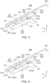
- a multiband antenna 1 0A of a first modification is different from the multiband antenna 10 (see Fig. 1 ) of the aforementioned embodiment in that positions of feeding points 211A and 213A are different from those of the feeding points 211 and 213 (see Fig. 1 ).
- the positions of the feeding points 211A and 213A are nearer to an open portion 24 than to a coupling portion 205 in the first direction.
- the positions of the feeding points 211 and 213 or 211A and 213A may be changed according to intended antenna properties.
- a multiband antenna 10B of a second modification is different from the multiband antenna 10A (see Fig. 3 ) of the first modification in that a shape of an additional element 40B is different from that of the additional element 40 (see Fig. 3 ).
- the additional element 40B has an L-shape when viewed along the third direction.
- a size of a front edge 401B of the additional element 40B is larger than that of the front edge 401 of the additional element 40 in the first direction.
- a capacitance between the additional element 40B and a second slot edge portion 203 can be larger than that between the additional element 40 and the second slot edge portion 203.
- a larger capacitance can achieve a lower operating frequency and downsize the multiband antenna 10B.
- a multiband antenna 10C of a third modification is different from the multiband antenna 10 (see Fig. 1 ) of the aforementioned embodiment in that it has a grounding terminal 60C which has a part extending in a direction intersecting with the specific plane or the X-Y plane.
- the grounding terminal 60C has a rectangular flat plate-like shape, and the whole thereof extends downward from a front edge of a second slot edge portion 203.
- the grounding terminal 60C may extend forward from the front edge of the second slot edge portion 203 and then extend the direction intersecting with the specific plane.
- the part extending in the direction intersecting with the specific plane may be on a plane perpendicular to the first direction or on a plane perpendicular to the second direction.
- a multiband antenna 10D of a fourth modification is different from the multiband antenna 10C (see Fig. 5 ) of the third modification in that a position of a grounding terminal 60D is different from that of the grounding terminal 60C (see Fig. 5 ).
- the grounding terminal 60D is positioned apart from both ends of a second slot edge portion 203 in the first direction. Moreover, the grounding terminal 60D is nearer to an open portion 24 than to a coupling portion 205 in the first direction. Thus, in the present invention, the position of the grounding terminal 60, 60C or 60D may be changed according to intended antenna properties.
- a multiband antenna 10E of a fifth modification is different from the multiband antenna 10C (see Fig. 5 ) of the third modification in that it has an additional grounding terminal 60E in addition to a grounding terminal 60C.
- the additional grounding terminal 60E extends downward from a front edge of an end portion 2033 of a second slot edge portion 203.
- the additional grounding terminal 60E helps to improve reliability of the multiband antenna 10E.
- the multiband antenna of the present invention can be provided with any number of grounding terminals.
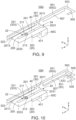
- a multiband antenna 10F of a sixth modification is different from the multiband antenna 10C (see Fig. 5 ) of the third modification in that a shape of a second radiation element 50F is different from that of the second radiation element 50 (see Fig. 5 ).
- the second radiation element 50F has an extension portion 505 in addition to a long portion 501 and a short portion 503.
- the extension portion 505 extends from a front-end portion of the short portion 503 in the second orientation.
- the extension portion 505 can lengthen an electrical length of the second radiation element 50F without increasing a size of the second radiation element 50F in the first direction.
- a shape of the second radiation element 50 or 50F may be changed according to intended antenna properties.
- a multiband antenna 10G of a seventh modification is different from the multiband antenna 10F (see Fig. 8 ) of the sixth modification in that a shape of a second radiation element 50G is different from that of the second radiation element 50F (see Fig. 8 ).
- the second radiation element 50G has a vertical portion 507 in addition to the structure of the second radiation element 50F.
- the vertical portion 507 extends downward from a rear edge of a long portion 501. In the first direction, a size of the vertical portion 507 is smaller than that of the long portion 501.
- the vertical portion 507 helps to improve strength and radiation properties of the second radiation element 50G.
- a shape of the second radiation element 50, 50F or 50G may be changed according to intended antenna properties.
- a multiband antenna 10H of an eighth modification is different from the multiband antenna 10G (see Fig. 9 ) of the seventh modification in that it is provided with a third radiation element 53.
- the third radiation element 53 has an additional long portion 531, an additional short portion 533 and an additional extension portion 535.
- the third radiation element 53 is formed so that it is substantially same as a second radiation element 50G.
- the additional long portion 531 is coupled with a lower edge of a vertical portion 507.
- the third radiation element 53 overlaps with the second radiation element 50G.
- the number of radiation elements or passive antennas i.e., the number of operating frequencies or an operating frequency band can be freely set.
- a multiband antenna 101 of a ninth modification is different from the multiband antenna 10C (see Fig. 5 ) of the third modification in that it is provided with a fourth radiation element 55.
- the fourth radiation element 55 has a rectangular shape long in the first direction.
- the fourth radiation element 55 extends from an end portion 2011 of a first slot edge portion 201 in the first orientation.
- a size of the fourth radiation element 55 is equal to or less than half of a size of a long portion 501 of a second radiation element 50.
- the present invention is not limited thereto.
- the shape and the size of the fourth radiation element 55 may be freely set according to intended antenna properties.
- a multiband antenna 10J of a tenth modification is different from the multiband antenna 10C (see Fig. 5 ) of the third modification in that it is provided with a fifth radiation element 57.
- the fifth radiation element 57 has a rectangular shape long in the first direction.
- the fifth radiation element 57 extends from an end portion 2031 of a second slot edge portion 203 in the first orientation.
- a size of the fifth radiation element 57 is equal to or less than half of a size of a long portion 501 of a second radiation element 50.
- the present invention is not limited thereto.
- the shape and the size of the fifth radiation element 57 may be freely set according to intended antenna properties.
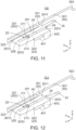
- a multiband antenna 10K of an eleventh modification is different from the multiband antenna 10E (see Fig. 7 ) of the fifth modification in that it is provided with a feeding terminal 62.
- the feeding terminal 62 has a part extending in a direction intersecting with the specific plane.
- the feeding terminal 62 has a rectangular flat plate-like shape, and the whole thereof extends downward from a front edge of a first slot edge portion 201.
- the feeding terminal 62 may extend forward from the front edge of the first slot edge portion 201 and then extend the direction intersecting with the specific plane.
- the part extending in the direction intersecting with the specific plane may be on a plane perpendicular to the first direction or on a plane perpendicular to the second direction.
- a size of the feeding terminal 62 is equal to that of a grounding terminal 60C and to that of an additional grounding terminal 60E.
- the multiband antenna 10K can be surface mounted on an object (not shown), such as a circuit board.
- an object such as a circuit board.
- the feeding terminal 62, the grounding terminal 60C and the additional grounding terminal 60E can be connected to the conductive patterns 80 corresponding to them, respectively.
- a multiband antenna 10L of a twelfth modification is different from the multiband antenna 10 (see Fig. 2 ) of the aforementioned embodiment in that it further has a first extension slot edge portion 207.
- the first extension slot edge portion 207 has an L-shape when viewed along the third direction.
- the first extension slot edge portion 207 extends from an end portion 2011 of a first slot edge portion 201 in the first orientation and then extends forward.
- an open portion 24L is formed at a part of a conductive main portion 20 which is different from the first slot edge portion 201.
- the open portion 24L is located between a front edge of a second slot edge portion 203 and a front edge of the first extension slot edge portion 207 and opened forward.
- a multiband antenna 10M of a thirteenth modification is different from the multiband antenna 10 (see Fig. 2 ) of the aforementioned embodiment in that it further has a first extension slot edge portion 207M and a second extension slot edge portion 209.
- the first extension slot edge portion 207M has a rectangular shape and extends from an end portion 2011 of a first slot edge portion 201 in the first orientation.
- the second extension slot edge portion 209 has an inverted L-shape when viewed along the third direction.
- the second extension slot edge portion 209 extends from an end portion 2031 of a second slot edge portion 203 in the first orientation and then extends rearward.
- an open portion 24M is formed at a part of a conductive main portion 20 which is different from the first slot edge portion 201.
- the open portion 24M is located between a rear edge of the first extension slot edge portion 207M and a rear edge of the second extension slot edge portion 209 and opened rearward.
- a multiband antenna 10N of a fourteenth modification is different from the multiband antenna 10 (see Fig. 2 ) of the aforementioned embodiment in that a shape of an additional element 40N is different from that of the additional element 40 (see Fig. 2 ).
- the additional element 40N of the present modification has in common with the additional element 40 in that it extends toward a second specific area 75 through a first specific area 70.
- the additional element 40N of the present modification has a crank shape when viewed along the third direction.
- the additional element 40N of the present modification extends forward from a lower end of a rear portion 323 of a first radiation element 30 and then extends in the first orientation and further extends forward.
- each of the first specific area 70 and the second specific area 75 is an area on a plane which is perpendicular to the third direction and which is positioned apart from the specific plane in the third direction.
- the first specific area 70 is an area overlapping with a first slot edge portion 201 in the third direction.
- the second specific area 75 is an area overlapping with a second slot edge portion 203 in the third direction.
- the additional element 40N is located on a plane where the first specific area 70 and the second specific area 75 are included, and a front edge 401N of the additional element 40N is in the second specific area 75.
- the additional element 40N forms a capacitance between itself and the second slot edge portion 203 and adjusts an impedance of the multiband antenna 10N, so that it lowers operating frequencies of the multiband antenna 10N or helps to downsize the multiband antenna 10N.
Landscapes
- Waveguide Aerials (AREA)
Applications Claiming Priority (1)
| Application Number | Priority Date | Filing Date | Title |
|---|---|---|---|
| JP2022068160A JP7748911B2 (ja) | 2022-04-18 | 2022-04-18 | マルチバンドアンテナ |
Publications (2)
| Publication Number | Publication Date |
|---|---|
| EP4266499A1 EP4266499A1 (en) | 2023-10-25 |
| EP4266499B1 true EP4266499B1 (en) | 2024-10-30 |
Family
ID=85792015
Family Applications (1)
| Application Number | Title | Priority Date | Filing Date |
|---|---|---|---|
| EP23165262.9A Active EP4266499B1 (en) | 2022-04-18 | 2023-03-29 | Multiband antenna |
Country Status (6)
| Country | Link |
|---|---|
| US (1) | US12401119B2 (https=) |
| EP (1) | EP4266499B1 (https=) |
| JP (1) | JP7748911B2 (https=) |
| KR (1) | KR102680791B1 (https=) |
| CN (1) | CN116914436A (https=) |
| TW (1) | TWI856593B (https=) |
Family Cites Families (15)
| Publication number | Priority date | Publication date | Assignee | Title |
|---|---|---|---|---|
| AU6863500A (en) | 1999-09-10 | 2001-04-17 | Galtronics Ltd. | Broadband or multi-band planar antenna |
| DE10231961B3 (de) * | 2002-07-15 | 2004-02-12 | Kathrein-Werke Kg | Niedrig bauende Dual- oder Multibandantenne, insbesondere für Kraftfahrzeuge |
| JP2006129226A (ja) | 2004-10-29 | 2006-05-18 | Hitachi Cable Ltd | 基板搭載薄型アンテナ |
| FI20055353A0 (fi) * | 2005-06-28 | 2005-06-28 | Lk Products Oy | Sisäinen monikaista-antenni |
| JP2007129597A (ja) | 2005-11-07 | 2007-05-24 | Nissei Electric Co Ltd | 多周波アンテナ |
| US7911387B2 (en) * | 2007-06-21 | 2011-03-22 | Apple Inc. | Handheld electronic device antennas |
| US7612725B2 (en) * | 2007-06-21 | 2009-11-03 | Apple Inc. | Antennas for handheld electronic devices with conductive bezels |
| US8441404B2 (en) * | 2007-12-18 | 2013-05-14 | Apple Inc. | Feed networks for slot antennas in electronic devices |
| JP5699820B2 (ja) | 2010-09-16 | 2015-04-15 | 日本電気株式会社 | アンテナ装置 |
| CN102790262B (zh) | 2011-05-19 | 2014-11-05 | 光宝电子(广州)有限公司 | 天线与具有该天线的电子装置 |
| JP7216576B2 (ja) * | 2019-03-05 | 2023-02-01 | 日本航空電子工業株式会社 | アンテナ |
| JP7475126B2 (ja) | 2019-10-29 | 2024-04-26 | 日本航空電子工業株式会社 | アンテナ |
| JP7508237B2 (ja) | 2020-02-26 | 2024-07-01 | 日本航空電子工業株式会社 | マルチバンドアンテナ |
| KR102831684B1 (ko) * | 2020-04-10 | 2025-07-08 | 엘에스일렉트릭(주) | 배전 시스템 |
| CN112909511B (zh) * | 2021-02-05 | 2023-03-17 | 哈尔滨工程大学 | 一种多频带5g终端天线 |
-
2022
- 2022-04-18 JP JP2022068160A patent/JP7748911B2/ja active Active
-
2023
- 2023-03-16 KR KR1020230034720A patent/KR102680791B1/ko active Active
- 2023-03-16 CN CN202310266949.5A patent/CN116914436A/zh active Pending
- 2023-03-28 US US18/127,176 patent/US12401119B2/en active Active
- 2023-03-29 EP EP23165262.9A patent/EP4266499B1/en active Active
- 2023-03-31 TW TW112112481A patent/TWI856593B/zh active
Also Published As
| Publication number | Publication date |
|---|---|
| JP2023158364A (ja) | 2023-10-30 |
| TWI856593B (zh) | 2024-09-21 |
| JP7748911B2 (ja) | 2025-10-03 |
| EP4266499A1 (en) | 2023-10-25 |
| CN116914436A (zh) | 2023-10-20 |
| US20230335901A1 (en) | 2023-10-19 |
| KR102680791B1 (ko) | 2024-07-02 |
| US12401119B2 (en) | 2025-08-26 |
| KR20230148741A (ko) | 2023-10-25 |
| TW202347882A (zh) | 2023-12-01 |
Similar Documents
| Publication | Publication Date | Title |
|---|---|---|
| US7053844B2 (en) | Integrated multiband antennas for computing devices | |
| US7791546B2 (en) | Antenna device and electronic apparatus | |
| JP5060629B1 (ja) | アンテナ装置とこのアンテナ装置を備えた電子機器 | |
| US7034754B2 (en) | Multi-band antenna | |
| CN102884679B (zh) | 天线装置 | |
| US20050030239A1 (en) | Antenna of small dimensions | |
| TWI768843B (zh) | 天線模組及電子裝置 | |
| EP2063488A1 (en) | Dual band antenna | |
| CN112821039B (zh) | 天线结构及电子装置 | |
| US7230573B2 (en) | Dual-band antenna with an impedance transformer | |
| TW201320468A (zh) | 槽孔天線 | |
| US10211533B2 (en) | Dual band printed antenna | |
| US20180287249A1 (en) | Antenna apparatus and electronic device | |
| EP4092827B1 (en) | Multiband antenna | |
| EP4266499B1 (en) | Multiband antenna | |
| JP5092066B2 (ja) | アンテナ装置とこのアンテナ装置を備えた電子機器 | |
| CN2906951Y (zh) | 采用回型振子的三频pcb天线 | |
| US20040222922A1 (en) | Multi-band printed monopole antenna | |
| EP4668479A1 (en) | Planar antenna | |
| CN218827822U (zh) | WiFi双频天线 | |
| CN117353006B (zh) | 地辐射天线及通信设备 | |
| CN2906952Y (zh) | 采用回型振子的双频pcb天线 | |
| CN2896554Y (zh) | 采用回型振子的单频pcb天线 | |
| KR20010111334A (ko) | 다중대역 세라믹 내장형 안테나 | |
| CN118676585A (zh) | 天线组件及电子设备 |
Legal Events
| Date | Code | Title | Description |
|---|---|---|---|
| STAA | Information on the status of an ep patent application or granted ep patent |
Free format text: STATUS: THE APPLICATION HAS BEEN PUBLISHED |
|
| PUAI | Public reference made under article 153(3) epc to a published international application that has entered the european phase |
Free format text: ORIGINAL CODE: 0009012 |
|
| AK | Designated contracting states |
Kind code of ref document: A1 Designated state(s): AL AT BE BG CH CY CZ DE DK EE ES FI FR GB GR HR HU IE IS IT LI LT LU LV MC ME MK MT NL NO PL PT RO RS SE SI SK SM TR |
|
| STAA | Information on the status of an ep patent application or granted ep patent |
Free format text: STATUS: REQUEST FOR EXAMINATION WAS MADE |
|
| 17P | Request for examination filed |
Effective date: 20240223 |
|
| RBV | Designated contracting states (corrected) |
Designated state(s): AL AT BE BG CH CY CZ DE DK EE ES FI FR GB GR HR HU IE IS IT LI LT LU LV MC ME MK MT NL NO PL PT RO RS SE SI SK SM TR |
|
| GRAP | Despatch of communication of intention to grant a patent |
Free format text: ORIGINAL CODE: EPIDOSNIGR1 |
|
| STAA | Information on the status of an ep patent application or granted ep patent |
Free format text: STATUS: GRANT OF PATENT IS INTENDED |
|
| INTG | Intention to grant announced |
Effective date: 20240531 |
|
| GRAS | Grant fee paid |
Free format text: ORIGINAL CODE: EPIDOSNIGR3 |
|
| GRAA | (expected) grant |
Free format text: ORIGINAL CODE: 0009210 |
|
| STAA | Information on the status of an ep patent application or granted ep patent |
Free format text: STATUS: THE PATENT HAS BEEN GRANTED |
|
| AK | Designated contracting states |
Kind code of ref document: B1 Designated state(s): AL AT BE BG CH CY CZ DE DK EE ES FI FR GB GR HR HU IE IS IT LI LT LU LV MC ME MK MT NL NO PL PT RO RS SE SI SK SM TR |
|
| RAP3 | Party data changed (applicant data changed or rights of an application transferred) |
Owner name: JAPAN AVIATION ELECTRONICS INDUSTRY, LIMITED |
|
| REG | Reference to a national code |
Ref country code: GB Ref legal event code: FG4D |
|
| REG | Reference to a national code |
Ref country code: CH Ref legal event code: EP |
|
| REG | Reference to a national code |
Ref country code: DE Ref legal event code: R096 Ref document number: 602023000854 Country of ref document: DE |
|
| REG | Reference to a national code |
Ref country code: IE Ref legal event code: FG4D |
|
| REG | Reference to a national code |
Ref country code: LT Ref legal event code: MG9D |
|
| REG | Reference to a national code |
Ref country code: NL Ref legal event code: MP Effective date: 20241030 |
|
| PG25 | Lapsed in a contracting state [announced via postgrant information from national office to epo] |
Ref country code: IS Free format text: LAPSE BECAUSE OF FAILURE TO SUBMIT A TRANSLATION OF THE DESCRIPTION OR TO PAY THE FEE WITHIN THE PRESCRIBED TIME-LIMIT Effective date: 20250228 Ref country code: HR Free format text: LAPSE BECAUSE OF FAILURE TO SUBMIT A TRANSLATION OF THE DESCRIPTION OR TO PAY THE FEE WITHIN THE PRESCRIBED TIME-LIMIT Effective date: 20241030 Ref country code: PT Free format text: LAPSE BECAUSE OF FAILURE TO SUBMIT A TRANSLATION OF THE DESCRIPTION OR TO PAY THE FEE WITHIN THE PRESCRIBED TIME-LIMIT Effective date: 20250228 |
|
| PG25 | Lapsed in a contracting state [announced via postgrant information from national office to epo] |
Ref country code: NL Free format text: LAPSE BECAUSE OF FAILURE TO SUBMIT A TRANSLATION OF THE DESCRIPTION OR TO PAY THE FEE WITHIN THE PRESCRIBED TIME-LIMIT Effective date: 20241030 Ref country code: FI Free format text: LAPSE BECAUSE OF FAILURE TO SUBMIT A TRANSLATION OF THE DESCRIPTION OR TO PAY THE FEE WITHIN THE PRESCRIBED TIME-LIMIT Effective date: 20241030 |
|
| REG | Reference to a national code |
Ref country code: AT Ref legal event code: MK05 Ref document number: 1737856 Country of ref document: AT Kind code of ref document: T Effective date: 20241030 |
|
| PG25 | Lapsed in a contracting state [announced via postgrant information from national office to epo] |
Ref country code: BG Free format text: LAPSE BECAUSE OF FAILURE TO SUBMIT A TRANSLATION OF THE DESCRIPTION OR TO PAY THE FEE WITHIN THE PRESCRIBED TIME-LIMIT Effective date: 20241030 |
|
| PG25 | Lapsed in a contracting state [announced via postgrant information from national office to epo] |
Ref country code: ES Free format text: LAPSE BECAUSE OF FAILURE TO SUBMIT A TRANSLATION OF THE DESCRIPTION OR TO PAY THE FEE WITHIN THE PRESCRIBED TIME-LIMIT Effective date: 20241030 |
|
| PG25 | Lapsed in a contracting state [announced via postgrant information from national office to epo] |
Ref country code: NO Free format text: LAPSE BECAUSE OF FAILURE TO SUBMIT A TRANSLATION OF THE DESCRIPTION OR TO PAY THE FEE WITHIN THE PRESCRIBED TIME-LIMIT Effective date: 20250130 |
|
| PG25 | Lapsed in a contracting state [announced via postgrant information from national office to epo] |
Ref country code: AT Free format text: LAPSE BECAUSE OF FAILURE TO SUBMIT A TRANSLATION OF THE DESCRIPTION OR TO PAY THE FEE WITHIN THE PRESCRIBED TIME-LIMIT Effective date: 20241030 Ref country code: LV Free format text: LAPSE BECAUSE OF FAILURE TO SUBMIT A TRANSLATION OF THE DESCRIPTION OR TO PAY THE FEE WITHIN THE PRESCRIBED TIME-LIMIT Effective date: 20241030 Ref country code: GR Free format text: LAPSE BECAUSE OF FAILURE TO SUBMIT A TRANSLATION OF THE DESCRIPTION OR TO PAY THE FEE WITHIN THE PRESCRIBED TIME-LIMIT Effective date: 20250131 |
|
| PG25 | Lapsed in a contracting state [announced via postgrant information from national office to epo] |
Ref country code: PL Free format text: LAPSE BECAUSE OF FAILURE TO SUBMIT A TRANSLATION OF THE DESCRIPTION OR TO PAY THE FEE WITHIN THE PRESCRIBED TIME-LIMIT Effective date: 20241030 |
|
| PG25 | Lapsed in a contracting state [announced via postgrant information from national office to epo] |
Ref country code: RS Free format text: LAPSE BECAUSE OF FAILURE TO SUBMIT A TRANSLATION OF THE DESCRIPTION OR TO PAY THE FEE WITHIN THE PRESCRIBED TIME-LIMIT Effective date: 20250130 |
|
| PG25 | Lapsed in a contracting state [announced via postgrant information from national office to epo] |
Ref country code: SM Free format text: LAPSE BECAUSE OF FAILURE TO SUBMIT A TRANSLATION OF THE DESCRIPTION OR TO PAY THE FEE WITHIN THE PRESCRIBED TIME-LIMIT Effective date: 20241030 |
|
| PG25 | Lapsed in a contracting state [announced via postgrant information from national office to epo] |
Ref country code: DK Free format text: LAPSE BECAUSE OF FAILURE TO SUBMIT A TRANSLATION OF THE DESCRIPTION OR TO PAY THE FEE WITHIN THE PRESCRIBED TIME-LIMIT Effective date: 20241030 |
|
| PG25 | Lapsed in a contracting state [announced via postgrant information from national office to epo] |
Ref country code: EE Free format text: LAPSE BECAUSE OF FAILURE TO SUBMIT A TRANSLATION OF THE DESCRIPTION OR TO PAY THE FEE WITHIN THE PRESCRIBED TIME-LIMIT Effective date: 20241030 |
|
| PG25 | Lapsed in a contracting state [announced via postgrant information from national office to epo] |
Ref country code: RO Free format text: LAPSE BECAUSE OF FAILURE TO SUBMIT A TRANSLATION OF THE DESCRIPTION OR TO PAY THE FEE WITHIN THE PRESCRIBED TIME-LIMIT Effective date: 20241030 |
|
| PG25 | Lapsed in a contracting state [announced via postgrant information from national office to epo] |
Ref country code: SK Free format text: LAPSE BECAUSE OF FAILURE TO SUBMIT A TRANSLATION OF THE DESCRIPTION OR TO PAY THE FEE WITHIN THE PRESCRIBED TIME-LIMIT Effective date: 20241030 |
|
| PG25 | Lapsed in a contracting state [announced via postgrant information from national office to epo] |
Ref country code: CZ Free format text: LAPSE BECAUSE OF FAILURE TO SUBMIT A TRANSLATION OF THE DESCRIPTION OR TO PAY THE FEE WITHIN THE PRESCRIBED TIME-LIMIT Effective date: 20241030 |
|
| PG25 | Lapsed in a contracting state [announced via postgrant information from national office to epo] |
Ref country code: IT Free format text: LAPSE BECAUSE OF FAILURE TO SUBMIT A TRANSLATION OF THE DESCRIPTION OR TO PAY THE FEE WITHIN THE PRESCRIBED TIME-LIMIT Effective date: 20241030 |
|
| REG | Reference to a national code |
Ref country code: DE Ref legal event code: R097 Ref document number: 602023000854 Country of ref document: DE |
|
| PLBE | No opposition filed within time limit |
Free format text: ORIGINAL CODE: 0009261 |
|
| STAA | Information on the status of an ep patent application or granted ep patent |
Free format text: STATUS: NO OPPOSITION FILED WITHIN TIME LIMIT |
|
| PG25 | Lapsed in a contracting state [announced via postgrant information from national office to epo] |
Ref country code: SE Free format text: LAPSE BECAUSE OF FAILURE TO SUBMIT A TRANSLATION OF THE DESCRIPTION OR TO PAY THE FEE WITHIN THE PRESCRIBED TIME-LIMIT Effective date: 20241030 |
|
| 26N | No opposition filed |
Effective date: 20250731 |
|
| PG25 | Lapsed in a contracting state [announced via postgrant information from national office to epo] |
Ref country code: MC Free format text: LAPSE BECAUSE OF FAILURE TO SUBMIT A TRANSLATION OF THE DESCRIPTION OR TO PAY THE FEE WITHIN THE PRESCRIBED TIME-LIMIT Effective date: 20241030 |
|
| PG25 | Lapsed in a contracting state [announced via postgrant information from national office to epo] |
Ref country code: LU Free format text: LAPSE BECAUSE OF NON-PAYMENT OF DUE FEES Effective date: 20250329 |
|
| REG | Reference to a national code |
Ref country code: BE Ref legal event code: MM Effective date: 20250331 |
|
| PG25 | Lapsed in a contracting state [announced via postgrant information from national office to epo] |
Ref country code: BE Free format text: LAPSE BECAUSE OF NON-PAYMENT OF DUE FEES Effective date: 20250331 |
|
| PG25 | Lapsed in a contracting state [announced via postgrant information from national office to epo] |
Ref country code: IE Free format text: LAPSE BECAUSE OF NON-PAYMENT OF DUE FEES Effective date: 20250329 |
|
| PGFP | Annual fee paid to national office [announced via postgrant information from national office to epo] |
Ref country code: DE Payment date: 20260204 Year of fee payment: 4 |
|
| PGFP | Annual fee paid to national office [announced via postgrant information from national office to epo] |
Ref country code: FR Payment date: 20260209 Year of fee payment: 4 |