EP4265072B1 - Vorrichtung zur abscheidung von dünnschichten mit hilfe von mikrowellenplasma - Google Patents
Vorrichtung zur abscheidung von dünnschichten mit hilfe von mikrowellenplasma Download PDFInfo
- Publication number
- EP4265072B1 EP4265072B1 EP21851684.7A EP21851684A EP4265072B1 EP 4265072 B1 EP4265072 B1 EP 4265072B1 EP 21851684 A EP21851684 A EP 21851684A EP 4265072 B1 EP4265072 B1 EP 4265072B1
- Authority
- EP
- European Patent Office
- Prior art keywords
- plasma
- thin film
- film deposition
- target
- face
- Prior art date
- Legal status (The legal status is an assumption and is not a legal conclusion. Google has not performed a legal analysis and makes no representation as to the accuracy of the status listed.)
- Active
Links
Images


Classifications
-
- H—ELECTRICITY
- H01—ELECTRIC ELEMENTS
- H01J—ELECTRIC DISCHARGE TUBES OR DISCHARGE LAMPS
- H01J37/00—Discharge tubes with provision for introducing objects or material to be exposed to the discharge, e.g. for the purpose of examination or processing thereof
- H01J37/32—Gas-filled discharge tubes
- H01J37/34—Gas-filled discharge tubes operating with cathodic sputtering
- H01J37/3411—Constructional aspects of the reactor
- H01J37/345—Magnet arrangements in particular for cathodic sputtering apparatus
- H01J37/3452—Magnet distribution
-
- C—CHEMISTRY; METALLURGY
- C23—COATING METALLIC MATERIAL; COATING MATERIAL WITH METALLIC MATERIAL; CHEMICAL SURFACE TREATMENT; DIFFUSION TREATMENT OF METALLIC MATERIAL; COATING BY VACUUM EVAPORATION, BY SPUTTERING, BY ION IMPLANTATION OR BY CHEMICAL VAPOUR DEPOSITION, IN GENERAL; INHIBITING CORROSION OF METALLIC MATERIAL OR INCRUSTATION IN GENERAL
- C23C—COATING METALLIC MATERIAL; COATING MATERIAL WITH METALLIC MATERIAL; SURFACE TREATMENT OF METALLIC MATERIAL BY DIFFUSION INTO THE SURFACE, BY CHEMICAL CONVERSION OR SUBSTITUTION; COATING BY VACUUM EVAPORATION, BY SPUTTERING, BY ION IMPLANTATION OR BY CHEMICAL VAPOUR DEPOSITION, IN GENERAL
- C23C14/00—Coating by vacuum evaporation, by sputtering or by ion implantation of the coating forming material
- C23C14/0021—Reactive sputtering or evaporation
-
- C—CHEMISTRY; METALLURGY
- C23—COATING METALLIC MATERIAL; COATING MATERIAL WITH METALLIC MATERIAL; CHEMICAL SURFACE TREATMENT; DIFFUSION TREATMENT OF METALLIC MATERIAL; COATING BY VACUUM EVAPORATION, BY SPUTTERING, BY ION IMPLANTATION OR BY CHEMICAL VAPOUR DEPOSITION, IN GENERAL; INHIBITING CORROSION OF METALLIC MATERIAL OR INCRUSTATION IN GENERAL
- C23C—COATING METALLIC MATERIAL; COATING MATERIAL WITH METALLIC MATERIAL; SURFACE TREATMENT OF METALLIC MATERIAL BY DIFFUSION INTO THE SURFACE, BY CHEMICAL CONVERSION OR SUBSTITUTION; COATING BY VACUUM EVAPORATION, BY SPUTTERING, BY ION IMPLANTATION OR BY CHEMICAL VAPOUR DEPOSITION, IN GENERAL
- C23C14/00—Coating by vacuum evaporation, by sputtering or by ion implantation of the coating forming material
- C23C14/22—Coating by vacuum evaporation, by sputtering or by ion implantation of the coating forming material characterised by the process of coating
- C23C14/24—Vacuum evaporation
- C23C14/32—Vacuum evaporation by explosion; by evaporation and subsequent ionisation of the vapours, e.g. ion-plating
-
- H—ELECTRICITY
- H01—ELECTRIC ELEMENTS
- H01J—ELECTRIC DISCHARGE TUBES OR DISCHARGE LAMPS
- H01J37/00—Discharge tubes with provision for introducing objects or material to be exposed to the discharge, e.g. for the purpose of examination or processing thereof
- H01J37/32—Gas-filled discharge tubes
- H01J37/32009—Arrangements for generation of plasma specially adapted for examination or treatment of objects, e.g. plasma sources
- H01J37/32192—Microwave generated discharge
- H01J37/32211—Means for coupling power to the plasma
- H01J37/32229—Waveguides
-
- H—ELECTRICITY
- H01—ELECTRIC ELEMENTS
- H01J—ELECTRIC DISCHARGE TUBES OR DISCHARGE LAMPS
- H01J37/00—Discharge tubes with provision for introducing objects or material to be exposed to the discharge, e.g. for the purpose of examination or processing thereof
- H01J37/32—Gas-filled discharge tubes
- H01J37/32431—Constructional details of the reactor
- H01J37/3266—Magnetic control means
- H01J37/32678—Electron cyclotron resonance
-
- H—ELECTRICITY
- H01—ELECTRIC ELEMENTS
- H01J—ELECTRIC DISCHARGE TUBES OR DISCHARGE LAMPS
- H01J37/00—Discharge tubes with provision for introducing objects or material to be exposed to the discharge, e.g. for the purpose of examination or processing thereof
- H01J37/32—Gas-filled discharge tubes
- H01J37/34—Gas-filled discharge tubes operating with cathodic sputtering
- H01J37/3402—Gas-filled discharge tubes operating with cathodic sputtering using supplementary magnetic fields
- H01J37/3405—Magnetron sputtering
- H01J37/3408—Planar magnetron sputtering
-
- H—ELECTRICITY
- H01—ELECTRIC ELEMENTS
- H01J—ELECTRIC DISCHARGE TUBES OR DISCHARGE LAMPS
- H01J37/00—Discharge tubes with provision for introducing objects or material to be exposed to the discharge, e.g. for the purpose of examination or processing thereof
- H01J37/32—Gas-filled discharge tubes
- H01J37/34—Gas-filled discharge tubes operating with cathodic sputtering
- H01J37/3411—Constructional aspects of the reactor
- H01J37/3414—Targets
- H01J37/3417—Arrangements
-
- H—ELECTRICITY
- H05—ELECTRIC TECHNIQUES NOT OTHERWISE PROVIDED FOR
- H05H—PLASMA TECHNIQUE; PRODUCTION OF ACCELERATED ELECTRICALLY-CHARGED PARTICLES OR OF NEUTRONS; PRODUCTION OR ACCELERATION OF NEUTRAL MOLECULAR OR ATOMIC BEAMS
- H05H1/00—Generating plasma; Handling plasma
- H05H1/24—Generating plasma
- H05H1/46—Generating plasma using applied electromagnetic fields, e.g. high frequency or microwave energy
- H05H1/461—Microwave discharges
- H05H1/463—Microwave discharges using antennas or applicators
Definitions
- the present invention relates to a device for the deposition of thin films assisted by microwave plasma.
- the plasma thin film deposition process is based on the creation of atomic vapors by evaporation of the targets which will be deposited on a substrate as such or in the form of chemical compounds formed on the deposition surface when the plasma contains reactive chemical species (atoms, radicals, etc.).
- the document US5677012 describes a plasma-assisted evaporation deposition installation comprising an enclosure on a side wall of which is mounted a plasma gun, and on the bottom of which is arranged a crucible comprising the material to be evaporated called a target.
- the plasma generated by the plasma gun must be guided to the free surface of the target to cause its evaporation.
- Permanent magnets and a coil are implemented around the crucible to guide the plasma.
- This device is relatively complex, the guidance requires operation at very low pressure, between 0.18 Pa and 0.61 Pa. In addition, it requires very precise adjustment with regard to the intensity of the magnetic fields and the distance between the plasma gun and the target.
- This device being formed of two sub-devices with a very particular relative orientation, it is relatively bulky. The problems in terms of space and adjustment are accentuated when one wishes to make deposits on large surfaces, requiring the use of several of these devices in the same enclosure.
- the document US5230784 A describes a microwave plasma source comprising a microwave applicator whose waveguide is coaxial and is formed of a central passage and an external conductor. The sputtering target is mounted in the central passage, i.e.
- a device for deposition by evaporation or by plasma-assisted sputtering intended to be mounted through the wall of an enclosure, comprising a device for producing a microwave plasma by electron cyclotron resonance and a support for the target to be evaporated arranged at the center of the plasma production device.
- the device thus formed offers great compactness compared to the deposition devices of the state of the art. In addition, it does not require complex adjustment between the plasma source and the target. In addition, the device integrating the plasma source and the target in a single object, the integration of several of these devices in an enclosure is simplified. It can operate over a relatively wide pressure range, for example extending over more than three orders of magnitude.
- the target support comprises heating means in order to evaporate the target.
- the target can be partially or completely evaporated by the energetic electrons of the plasma.
- the device according to the invention does not require negatively polarizing the target of material to be deposited. As a result, there is no voltage drop at the cathode which usually generates highly energetic heavy species likely to damage the film covering the substrate.
- the evaporative deposition device according to the invention can implement the positive polarization of the target.
- the target is negatively biased.
- a device for deposition by evaporation or sputtering comprising an electron cyclotron resonance plasma generator which integrates within it the material to be evaporated or sputtered.
- the plasma reinforces, or even ensures in its entirety, the evaporation or sputtering of the target.
- the magnetic structure is arranged relative to the target so that the field lines cross the surface of the target.
- the deposition device is then very compact and the material to be evaporated is located as close as possible to the plasma generator, the energetic electrons of the plasma participating in the heating and evaporation of the material.
- a device for plasma-assisted thin film deposition comprising a device for producing a microwave plasma by electron cyclotron resonance and a support for a target material intended to form the thin film
- said device for producing a microwave plasma comprising a body with a longitudinal axis extending between a first longitudinal end face and a second longitudinal end face and provided with a central passage extending between the first longitudinal end face and the second longitudinal end face, said support being housed in said central passage, said first longitudinal end face being intended to be housed in an enclosure of a deposition installation
- said body comprising an annular passage for propagating a microwave electric field connected to a microwave electric field source, said annular passage surrounding the central passage and opening into the first longitudinal end face, at least one cavity surrounding the central passage and located near the first longitudinal end face, a magnetic structure housed in said cavity
- said support comprising a basket configured to house the target and positioned so that the free face of the target is in a plane of the first longitudinal end face or close to
- the evaporation means comprise means for positive polarization of the target material housed in the support.
- the evaporation means may include means for heating the target material housed in the support.
- the means of heating the target material are Joule effect or induction heating means.
- the spraying means comprise means for negatively polarizing the target material housed in the support.
- the device for the deposition plasma-assisted thin film may include means for cooling the target material housed in the support.
- the device for plasma-assisted thin film deposition comprises means for cooling the body of the device for producing a microwave plasma.
- the magnetic structure comprises at least one permanent magnet.
- the magnetic structure comprises at least one permanent magnet with radial magnetization.
- the magnetic structure comprises at least one permanent magnet with dipole axial magnetization.
- the magnetic structure comprises at least two permanent magnets with axial magnetization of opposite polarity.
- the device for plasma-assisted thin film deposition may comprise two concentric magnetic structures and the annular propagation passage may open into the first longitudinal end face between the two magnetic structures.
- the body of the device for producing a microwave plasma comprises an inner conductor and an outer conductor nested one inside the other and defining between them a part of the annular passage for propagation of the wave.
- the present application also relates to an installation for plasma-assisted thin film deposition on a substrate, as defined by claim 14, comprising a sealed enclosure, a substrate holder and at least one device for plasma-assisted thin film deposition according to the invention mounted in a sealed manner through a wall of the enclosure, such that the first longitudinal end face of the body is inside the enclosure.
- the wall of the enclosure is contained in a plane and the device for plasma-assisted thin film deposition is mounted in the wall such that intersections of the magnetic field lines and said wall are minimized.
- the plasma gas pressure in the enclosure is preferably between 0.065 Pa and 133 Pa.
- the deposition installation comprises means for polarizing and/or heating the substrate.
- the invention will be explained by describing in detail a plasma-assisted evaporation deposition plant and a device for plasma-assisted evaporation deposition. As will be explained below, the invention also relates to a device for plasma-assisted sputtering deposition and a plasma-assisted sputtering deposition plant.
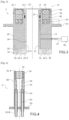
- FIG. 1 a schematic representation of a plasma-assisted evaporation ID deposition installation can be seen, incorporating a device for plasma-assisted evaporation deposition according to the invention.
- the installation comprises an enclosure E, a device for plasma-assisted evaporation deposition D1, and a substrate holder PS intended to support the substrate S on which the deposition is to be carried out.
- the substrate holder PS is generally arranged so that the substrate is opposite the device for plasma-assisted evaporation deposition.
- the device D1 is mounted through a wall of the enclosure, in the example shown this is the lower bottom F of the enclosure, but this arrangement is not limiting.
- the enclosure is intended to contain a plasma gas, for example at low or very low pressure, for example between 0.065 Pa and 133 Pa (0.5 mTorr and 1000 mTorr).
- the device for deposition D1 comprises a plasma generation device 2 and a device 4 configured to ensure the evaporation of the target material to be deposited on the substrate.
- the device for the deposit has a general form of revolution.
- the plasma generation device 2 is a device for generating a microwave plasma by electron cyclotron resonance.
- the operating principle of this device is to apply a high frequency electric field, for example 2.45 GHz, called microwave field to a plasma gas, in the presence of a magnetic field.
- a high frequency electric field for example 2.45 GHz
- microwave field By electron cyclotron resonance phenomenon or ECR a plasma is generated in the areas where the cyclotron frequency is equal to the frequency of the microwave field and is confined by the magnetic field.
- the device 2 This comprises a microwave coupler 6 and a magnetic structure 8.
- the microwave coupler 6 comprising a body 10 of longitudinal axis ZZ' provided with a central passage 12 of longitudinal axis opening at the two ends of the body 10.
- the body 10 comprises a first end face 14 intended to be arranged in the enclosure and located near the electron cyclotron resonance zone called the ECR zone, and a second end face 16 intended to be arranged outside the enclosure.
- the body 10 also comprises a channel 18 for propagating the microwave field of annular shape, surrounding the central passage 12 and opening into the first end face 14.
- the propagation channel 18 is connected to a high-frequency power generator 20, which delivers the microwave field, via a microwave power connector 22.
- the propagation channel delimits the propagation medium of the microwave field.
- the propagation medium may comprise air and/or a dielectric material with a permittivity other than 1.
- the propagation medium consists of air and an annular section 23 made of a dielectric material, for example alumina (Al 2 O 3 ), quartz or Teflon.
- the propagation medium includes a dielectric window, this is not necessarily intended to ensure vacuum sealing.
- the device can operate with or without an impedance adapter depending on the geometric design of the body 10, the HF frequency used, the nature and pressure of the plasma gas, the microwave power.
- an adapter impedance is implemented, it is inserted between the microwave power connector 22, and the high frequency power generator 20.
- the microwave field is guided along the entire length of the propagation channel from the microwave injection connector 22 to the first end face 14.
- the body 10 comprises an inner conductor 24 and an outer conductor 26 fitted into each other and defining between them a part of the propagation channel.
- the inner conductor 24 is designated “central core” and the outer conductor 26 is designated “shield”.
- the central core 24 comprises a tube 25.1 provided at one end 24.2 with a base 25.2 forming a flange, and the shield comprises a tube mounted around the tube 25.1 of the central core and one longitudinal end 26.2 of which rests on the flange 25.2.
- the other ends 24.1 of the central core and 26.1 of the shield form the first end face 14 of the coupler.
- the propagation channel 18 is delimited between the outer diameter of the central core 24 and the inner diameter of the shield 26.
- the contact between the flange 25.2 and the end 26.2 of the shield 26 is vacuum-tight.
- a seal (not shown) mounted in a groove 28 formed in the end of the coupler is provided.
- the central core 24 and the shield 26 are secured to each other, for example, by means of screws 30 mounted between the flange 25.2 and the end of the shield. Other means of securing are conceivable.
- the shield and the central core are made of the same metal, which is a very good electrical conductor and a very good thermal conductor with low microwave insertion losses.
- the metal can be chosen, for example, from silver, copper, aluminum and stainless steel. As a variant, different metals are used, for example, for reasons of brazing, welding and/or mechanical strength.
- the body 10 also comprises means for fixing through a wall of the enclosure.
- the shield 26 comprises on its outer face a flange 32 intended to come to bear against an inner face of the edge of an opening formed in the bottom F of the enclosure. Sealing means are also provided between the flange 32 and the wall of the enclosure.
- the flange 32 is positioned on the shield 26 so that the connection microwave either outside the enclosure.
- the flange 32 is fixed to the wall of the enclosure by mechanical fixing means, for example claws inside the enclosure.
- the external lateral face of the coupler comprises a thread cooperating with a tapping formed in the edge of the opening of the bottom wall.
- Means for cooling the coupler are preferably provided.
- a fluid circuit is formed in the flange 25.2 of the central core 24, the inlets 34 and outlet 36 of which are shown.
- the heat transfer medium used is, for example, water.
- separate heat transfer medium circulation circuits are implemented to cool the central core 24 and the shielding 26.
- the microwave coupler 6 also includes a housing for the magnetic structure 8 located as close as possible to the first end face 14.
- the housing is formed by an annular cavity 38 located in the end 26.1 of the shield and sized to receive the magnetic structure.
- the magnetic structure 8 comprises means for generating a magnetic field, preferably these are permanent magnets 42, which is favorable to the compactness of the device.
- one or more electromagnets are implemented, however they require an electrical power supply which makes the device more complex and more bulky.
- the cavity 38 is sealed by a cover 40 forming the first end face 14. Cooling of the magnets is also provided, for example the cooling circuit of the shield passes through the cavity 38. The assembly of the cover 40 on the shield is then liquid-tight.
- the magnetic structure 8 comprises one or more annular magnets 42. Magnets having magnetizations of different orientations can be used as will be detailed below. These can be radially magnetized magnets or axially magnetized magnets. The dimension of the magnets in the direction of the ZZ' axis can vary depending on the application.
- Non-magnetic shims 44 for example made of aluminum, can be inserted into the cavity 38 to adjust the position of the magnets along the axis. Indeed, the adjustment of the axial position of the magnets allows to adjust the position of the RCE zone and thus improve the plasma production efficiency.
- one or more shims may advantageously be arranged between the flange 32 and the bottom wall F to adjust the position of the device for deposition relative to the plane P2 of the bottom wall F.
- the use of the shims makes it possible to avoid having to manufacture several shields 26 whose flanges 32 would have different positions along the axis ZZ', which offers a certain flexibility in terms of adjusting the surface 14 relative to the bottom wall F of the chamber.
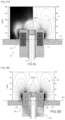
- the orientation of the magnetization and the axial dimension of the magnet(s) determine the shape of the field lines and the location and extent of the ECR zone or electron cyclotron resonance zone which make it possible to regulate the transport of the species of the plasma gas and vapor from the target to the deposition surface.
- the RCE reference designates the contour of the iso-B surface (875 gauss for a wave at 2.45 GHz) where the electrons absorb energy from the microwave field by resonance phenomenon.
- the RCE zone may partially, completely or not at all cover the surface of the target C.
- the magnets are positioned relative to the wall F of the enclosure through which the device D1 is preferably mounted such that the field lines B converge on the outer face of the shielding 26 and do not intersect or as little as possible the wall F of the enclosure to limit dry losses of plasma particles.
- the magnets are preferably positioned such that the field lines B converge on the outer face of the shielding at the level of the inner surface of the chamber.
- the magnetic structure comprises two 42.1 permanent magnets with axial magnetization mounted head to tail and forming an axial magnetization structure of opposite polarity.
- the arrows symbolize the orientation of the magnetization.
- the magnets have a dimension along the ZZ' axis larger than the magnets on the Figure 5A .
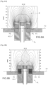
- the magnetic structure comprises a permanent magnet with radial magnetization 42.2.
- the arrows symbolize the orientation of the magnetization.
- the magnets have a smaller dimension along the ZZ' axis than the magnets on the Figure 6A .
- the magnetic structure comprises a permanent magnet with axial dipole magnetization 42.3.
- the arrows symbolize the orientation of the magnetization.
- a magnet with a dipole axial magnetization and a magnet with a radial magnetization of a desired length can be obtained by stacking several magnets of shorter lengths.
- magnet sectors are assembled. In the remainder of the description, we can therefore speak of a magnet or magnets of the magnetic structure.
- the magnets are arranged in the cavity so that, preferably, the contact plane P1 between the two magnets is coplanar with the plane P2 of the lower bottom F of the enclosure.
- the field lines B loop back into this plane P2, limiting the intersection of the field lines with the lower bottom of the enclosure as can be seen in the Figures 5A and 5B .
- the adjustment of the position of the plane P1 relative to the plane P2 can be obtained by means of non-magnetic shims, for example made of aluminum, of different thicknesses with transverse dimensions close to those of the magnets so that they can be housed in the cavity.
- the annular RCE zone does not cover the target, whereas on the Figure 5B it partially covers the target.
- the magnet 42.2 is arranged in the cavity so that, preferably, the median plane P3 of the magnet is coplanar with the plane P2 of the lower bottom of the enclosure.
- the magnetic field lines loop back into this plane P2, limiting the intersection of the field lines with the lower bottom of the enclosure as can be seen in the Figures 6A and 6B . Shims made of non-magnetic material can also be used.
- the RCE zone completely covers the end of the device for deposition in the enclosure forming an extended plasma production zone.
- the annular RCE zone does not cover the target.
- the magnet is arranged in the cavity so that, preferably, the plane P4 of a face of the magnet normal to the magnetization is coplanar with the plane P2 of the lower bottom of the enclosure.
- a part of the magnetic field lines B crosses the bottom of the enclosure as can be seen in the figure 7 . This leads to greater particle losses on the bottom wall of the chamber compared to the other structures indicated above.
- this configuration is acceptable because the plasma production is essentially distributed in front of the central part of the device and the orientation of the magnetic field lines favors the transport of particles towards the substrate.
- the annular RCE zone does not cover the target.
- One or more shims 44 may be arranged between the flange 32 and the bottom F of the enclosure to move the magnet away from the bottom and allow the field lines to loop back while limiting the intersection with the bottom.
- Shims 44 can be used to reposition the planes P2 and P4.
- the magnetic structure ensures an ECR surface covering at least one area around the microwave injection to avoid unnecessary radiation of the electromagnetic field.
- the ECR area can also completely cross the B-field lines and thus completely surround the structure ( Figure 6A ), which extends the area likely to produce plasma. It can also cross or not the surface of the target which allows, by varying the overlap area of the RCE surface and the surface of the target, to increase or reduce the flow of hot electrons contributing to the evaporation of the target.
- the device 4 configured to ensure the evaporation of the target material to be deposited on the substrate.
- the device 4 is configured to be housed in the central passage 12 of the microwave coupler and to position the target as close as possible to the first end face 14.
- the device 4 comprises a basket 46 intended to receive the target C to be evaporated and a support 48 supporting the basket 46 in order to arrange it as close as possible to the first end face.
- the support comprises two tubes 50 extending substantially axially along the direction of which a first end 50.1 supports the basket and a second end 50.2 passes through a fixing plate S2 at the second end face 16 of the coupler.
- the mounting of the tubes 50 in the fixing plate S2 and the mounting of the fixing plate on the second end face 16 of the coupler are vacuum-tight.
- the device 4 also comprises an element 54 forming a shield surrounding the basket and its support and providing electrical and thermal insulation, making it possible to limit the transfer of heat from the evaporator to the central core 24 of the coupler.
- the shield 54 is formed by a sleeve, in which the tubes 50 and the basket 46 are mounted.
- the device 4 comprises heating means 56 of the target carried by the first ends 50.1 of the tubes.
- the heating means 56 are of the Joule effect type and one or more electrical resistors in the form of wire conductors are housed in the inner face of the tube at right angles to the side wall of the basket.
- the tubes are made in two parts, a first solid part 58 carrying the basket and the heating means and a second hollow part 60 mounted in the fixing plate S2 and forming an electrical connector intended to be connected to a direct current generator 62 ( figure 1 ) for the electrical supply of the heating means.
- the second part 60 is hollow in order to advantageously allow its cooling.
- the heating of the target can be obtained by heating by oven.
- the heating means then comprise a resistance in the form of a cylinder surrounding the basket.
- the tubes 60 are also advantageously cooled in this variant.
- the heating means are induction heating means.
- the wire is supplied with a time-varying current, which creates a variable magnetic field, which induces a current in the target material and thus its heating.
- the target is brought to the temperature necessary for its evaporation by the heating means used and/or by the contribution of energetic electrons guided towards the surface of the target by the magnetic lines which intercept it.
- the basket material is adapted to the melting temperature of the target to avoid pollution of the deposit.
- the open end of the basket 46 may be arranged in alignment with, set back from, or ahead of the first end face 14. This positioning, chosen as a function of the type of heating and magnetic configuration used, may advantageously promote heating of the target surface and ionization of the vapors by the plasma electrons.
- the device 4 does not include heating means and the heating of the target for its evaporation is obtained solely by the energetic electrons of the plasma. Indeed, the energetic electrons having a speed parallel to the magnetic field lines intercepting the basket contribute to the evaporation. This flow can therefore contribute to the heating of the surface but without being sufficient to reach the temperature necessary for evaporation.
- the increase in the flow of electrons and the increase in their energy are obtained by the positive polarization of the target to obtain an electron current (of the order of a few amperes) sufficient for the evaporation of the surface of the target.
- device D2 comprising polarization means 64 comprising a voltage generator G of which one terminal is connected to the basket 46 and one terminal is connected to the enclosure.
- This example has the advantage of lifting the temperature limit imposed by the basket material. Indeed, when heating means are used and the melting temperature of the target material is high, the basket material must have a sufficiently high melting temperature so as not to risk the target material, few materials are usable, and the few materials generally used for the basket are alumina, silicon carbide and silicon nitride.
- the heating of the target is obtained jointly by the external heating means and by the flow of electrons increased by the positive polarization of the target.
- device D3 comprising polarization means 66, a voltage generator G of which one terminal is connected to the basket 46 and one terminal is connected to the enclosure and heating means 56 as described in relation to device D1.
- the polarization of the target is reduced compared to that of the previous embodiment and, as a result, the flow of electrons extracted from the plasma is lower.
- This embodiment has the advantage of limiting the depletion of the plasma in electrons and, at the same time, of reducing the external heating required. As a result, for materials with high evaporation points (close to the melting point of the basket) the risk of contamination is greatly reduced.
- Device 4 is positioned in device 2, more particularly target C is positioned inside the magnetic structure so that magnetic field lines B intercept the free surface of target C. Thus energetic electrons from the plasma strike target C and participate in the evaporation of the material.
- the substrate S on which the deposition is to be carried out is placed in the enclosure E on the substrate holder PS substantially opposite the device D1.
- the target C of material to be deposited is placed in the basket 46.
- the uniformity, the deposition rate and the properties of the deposited films are determined by the operating conditions such as the pressure and the composition of the plasma gas, the microwave power, the configuration of the magnetic field, the current of the external heating means, and the distance between the free surface of the target C and the substrate S.
- the plasma gas is chosen from Ar, O 2 , H 2 , or mixtures Ar/O 2 , Ar/H 2 , Ar/O 2 /H 2 , Ar/N 2 /O 2 , etc.
- Any reactive gas can be used as an additive to a carrier gas, generally argon, depending on the nature of the deposit to be made, for example an oxide, a hydride, a nitride, an oxynitride.
- a microwave field is injected into the coupler and the target C is heated by the heating means.
- the RCE zone allows a very efficient transfer of energy from the microwave electric field to the electrons which wrap around the B field lines ensuring their confinement, and At each passage in the RCE zone, statistically they gain energy. These electrons generate a plasma by collision with the neutral particles of the plasmagenic gas and the vapors coming from the target. In addition, field lines B intercepting the free surface of the target, energetic electrons of the plasma come to strike the target and participate in its evaporation. On the left part of the Figure 5A , the brightest areas are the areas populated with energetic electrons with a significant concentration at the target surface.
- Heavy species such as ions and neutrals, and thermalized electrons collectively diffuse through collisions, and are driven toward the deposition substrate, the target material then deposits on the substrate.
- the flux of plasma gas species is controlled mainly by power and pressure.
- the flux of plasma gas species and vapors can be determined by choosing an appropriate magnetic configuration according to which more or fewer field lines intercept the target, according to which an RCE zone is more or less distant, and/or more or less extensive.
- the target is not evaporated but sputtered.
- the structure of the sputtering deposition device D4 is similar to the evaporation deposition device, but it does not include means for heating the target, the sputtering of the target being obtained by negatively polarizing the target by a direct voltage in the case of an electrically conductive target material or by radio frequency in the case of an electrically non-conductive target material.
- the device includes polarization means 68, such as a direct DC, alternating AC or RF voltage generator, one terminal of which is connected to the target through the basket 46 and the other terminal is connected to the enclosure.
- the device D4 can be integrated into the enclosure of the figure 1 .
- This negative polarization of the target accelerates the ions to energies exceeding the sputtering threshold, of the order of 50 eV, of the target material.
- the atoms in the vapor phase are therefore obtained by plasma-assisted sputtering (reactive or not) instead of evaporation.
- This embodiment makes it possible to produce deposits with target materials requiring very high evaporation temperatures and/or electrical or dielectric conductors.
- the device for sputtering deposition comprises means for cooling the target, for example by circulating a liquid in a tube in contact with the target.
- This device is simpler to make than the device for evaporative deposition due to the absence of heating means.
- the enclosure has a diameter of the order of 300 mm allowing a photovoltaic cell of 150 mm ⁇ 150 mm to be housed.
- the device for the deposit has a diameter of the order of 200 mm.
- the basket has a diameter of the order of 25.4 mm.
- the coupler 102 comprises a magnetic structure comprising concentric magnets 142.1, 142.2 of axis ZZ' between which the propagation channel 118 of the microwave field is arranged.
- the device 104 can be configured to allow the evaporation of the target C with or without positive polarization similarly to the device 4 or be configured to allow the sputtering of the target by negatively polarizing it.
- the microwave injection channel is radially further away from the ZZ' axis of the coupler. This embodiment makes it possible to further extend the microwave power deposition area in the plasma and, in association with the magnetic field configuration, to increase the plasma production surface and thus the deposition surface by a unitary device.
- the device for the deposition having a reduced bulk it is possible to integrate several of these devices D in the same enclosure arranged spatially relative to each other to produce deposits on substrates of large surface area and/or having surfaces of complex shape.
- the cumulative effect between two devices in a close neighbor position contributes favorably to the homogenization of the plasma.
- the deposition devices can be arranged relative to each other at any distance with the only limit being the physical bulk of the unit device.
- the invention operating in evaporation mode, the risk of damage to the deposited layer by high-energy species is eliminated since it does not use a cathode at a highly negative potential, which is the source of creation of highly energetic species in the plasma.
- the device of the invention is free of cathodic drop since the coupler and its environment, just like the walls of the enclosure, are connected to ground. In the example where a positive polarization is applied to the target, this positive polarization also does not introduce cathodic drop.
- the operating pressure of the deposition plant is low, for example between 0.5 mTorr and 1000 mTorr (0.065 Pa and 133 Pa), it can nevertheless be considered to polarize the substrate when an ion-assisted deposition is desired. But even in this case, there is little or no risk of deterioration, since the kinetic energy of the ions on the deposition surface is perfectly controlled by the applied potentials and the plasma potential and, for low potentials, the energy input of the ions remains limited. -In addition, the substrate can be cooled to remove heat from the substrate.
- the evaporative deposition device according to the invention allows depositions to be carried out at high speeds compared to spray deposition speeds.
- the evaporation deposition device and the sputtering deposition device according to the invention make it possible to carry out low-temperature depositions of the substrate, without intentional cooling of the latter. Depositions on any type of substrate and in any material, for example plastic materials, are then possible.
- the evaporative deposition device and the spray deposition device according to the invention make it possible to carry out depositions on large surfaces by using as many devices as necessary.
- the device for evaporation deposition according to the invention has a high probability of ionization of the neutral vapor particles from the target by direct collisions with the plasma electrons thanks to the conditions existing near the target: high electron density, effective electron energy of the order of 10 eV to 20 eV, higher than the ionization threshold of vapors such as In (5.79 eV), Sn (7.34 eV), Mg (7.6 eV), Al (5.98 eV),..., high density of low energy vapors of the order of 0.03 eV).
- the device for evaporation deposition and the sputtering deposition device advantageously have a symmetry of revolution.
- the plasma becomes uniform beyond a certain distance from the end of the coupler, for example of the order of 20 cm, which makes it possible to produce uniform deposits.
- the structure of the evaporation deposition device for deposition is relatively simple, it is robust and offers high operational reliability.
- the structure of the spray deposition device for deposition is also very simple, or even simpler because the deposition device does not require heating means.
- the deposition device can be used for any type of vapor deposition where vapor phase particles are obtained by evaporation or spraying of the solid state material.
- the deposition device is suitable for different types of deposition. As explained, it also allows depositions to be carried out using ionic assistance by polarization of the substrate. It also allows depositions to be carried out at substrate temperatures controlled either by external heating or by cooling. For example, the substrate can be heated when the crystallization of the films or the selection of a crystallization phase requires more thermal energy.
- any type of electrical condition of the substrate (negative potential, grounded or floating) is allowed without changing the operation of the deposition device.
- the deposition device also offers great freedom in the choice of the nature of the reactive gas that can be used, since there is no reactivity with the materials present that would give rise to process drifts due to changes in plasma parameters during the process. This guarantees the reproducibility of the process.
- the device for deposition and the deposition installation comprising this device are particularly suitable for reactive plasma deposition on fragile substrates such as those made of plastic material, hydrogenated amorphous silicon, etc. or on materials which are themselves sensitive, for example Mg-based hydrides, AI-doped ZnO - AZO, at high temperature and/or bombardment by energetic particles from the plasma.
- fragile substrates such as those made of plastic material, hydrogenated amorphous silicon, etc. or on materials which are themselves sensitive, for example Mg-based hydrides, AI-doped ZnO - AZO, at high temperature and/or bombardment by energetic particles from the plasma.
- the deposition device can for example be used for the deposition of transparent conductors or TCO (Transparent Conducting Oxide in English terminology) commonly used in large surface applications and for the manufacture of solar cells, smart windows, touch screens and organic light-emitting diodes.
- TCO Transparent Conducting Oxide in English terminology
- the device can also be used for the deposition of ceramic or metallic films for the production of oxides, hydrides, oxynitrides such as SiOxNy, for example, used for the production of transparent barriers to water vapor.
Landscapes
- Chemical & Material Sciences (AREA)
- Engineering & Computer Science (AREA)
- Physics & Mathematics (AREA)
- Plasma & Fusion (AREA)
- Analytical Chemistry (AREA)
- Chemical Kinetics & Catalysis (AREA)
- Materials Engineering (AREA)
- Mechanical Engineering (AREA)
- Metallurgy (AREA)
- Organic Chemistry (AREA)
- Physical Vapour Deposition (AREA)
Claims (17)
- Vorrichtung zur plasmaunterstützten Dünnfilmabscheidung, eine Vorrichtung zur Erzeugung eines Mikrowellen-Plasmas durch elektronische Zyklotronresonanz (2) enthaltend, und einen Träger (4) eines Objektmaterials, das vorgesehen ist, um den Dünnfilm zu bilden, wobei die Vorrichtung zur Erzeugung eines Mikrowellen-Plasmas einen Körper (10) mit Längsachse (ZZ') enthält, der sich zwischen einer ersten Seite mit Längsende (14) und einer zweiten Seite mit Längsende (16) erstreckt und mit einem zentralen Durchgang (12) versehen ist, der sich zwischen der ersten Seite mit Längsende (14) und der zweiten Seite mit Längsende (16) erstreckt, wobei der Träger (4) im zentralen Durchgang (12) untergebracht ist, und die erste Seite mit Längsende (14) dazu bestimmt ist, in einem Gehäuse (E) einer Abscheidungsanlage untergebracht zu werden, wobei der Körper (10) einen ringförmigen Durchgang (18) zur Ausbreitung eines elektrischen Mikrowellenfelds enthält, der mit einer Quelle des elektrischen Mikrowellenfelds verbunden ist, wobei der ringförmige Durchgang (18) den zentralen Durchgang (12) umgibt und in die erste Seite mit Längsende (14) mündet, wobei mindestens ein Hohlraum (38) den zentralen Durchgang (12) umgibt und sich in der Nähe der ersten Seite mit Längsende (14) befindet, wobei eine magnetische Struktur (8) im Hohlraum (38) untergebracht ist, wobei der Träger (4) einen Korb (46) enthält, der konfiguriert ist, um das Objekt (C) unterzubringen, und so positioniert ist, dass die freie Seite des Objekts (C) in einer Ebene der ersten Seite mit Längsende (14) oder in der Nähe der Ebene liegt, und so, dass mindestens ein Teil der Feldlinien (B), die durch die magnetische Struktur (8) generiert werden, das Objekt (C) kreuzt, wobei die Abscheidungsvorrichtung auch Mittel zum Verdampfen oder Versprühen des Objektmaterials enthält.
- Vorrichtung zur plasmaunterstützten Dünnfilmabscheidung nach Anspruch 1, wobei die Verdampfungsmittel Mittel zur positiven Polarisation des Objektmaterials, die im Träger untergebracht sind, enthalten.
- Vorrichtung zur plasmaunterstützten Dünnfilmabscheidung nach Anspruch 1 oder 2, wobei die Verdampfungsmittel Mittel zum Erhitzen des Objektmaterials, das im Träger (4) untergebracht ist, enthalten.
- Vorrichtung zur plasmaunterstützten Dünnfilmabscheidung nach Anspruch 3, wobei die Mittel zur Erhitzung des Objektmaterials Erhitzungsmittel mit Joule-Effekt oder durch Induktion sind.
- Vorrichtung zur plasmaunterstützten Dünnfilmabscheidung nach Anspruch 1, wobei die Sprühmittel Mittel zur negativen Polarisation des Objektmaterials, das im Träger (4) untergebracht ist, enthalten.
- Vorrichtung zur plasmaunterstützten Dünnfilmabscheidung nach Anspruch 5, Mittel zum Abkühlen des Objektmaterials, das im Träger (4) untergebracht sind, enthaltend.
- Vorrichtung zur plasmaunterstützten Dünnfilmabscheidung nach einem der Ansprüche 1 bis 6, Mittel zum Abkühlen des Körpers der Vorrichtung zur Erzeugung eines Mikrowellen-Plasmas enthaltend.
- Vorrichtung zur plasmaunterstützten Dünnfilmabscheidung nach einem der Ansprüche 1 bis 7, wobei die magnetische Struktur (8) mindestens einen Permanentmagneten (42) enthält.
- Vorrichtung zur plasmaunterstützten Dünnfilmabscheidung nach einem der Ansprüche 1 bis 8, wobei die magnetische Struktur (8) mindestens einen radial magnetisierten Permanentmagneten (42.2) enthält.
- Vorrichtung zur plasmaunterstützten Dünnfilmabscheidung nach einem der Ansprüche 1 bis 8, wobei die magnetische Struktur (8) mindestens einen dipolaren axial magnetisierten Permanentmagneten (42.3) enthält.
- Vorrichtung zur plasmaunterstützten Dünnfilmabscheidung nach einem der Ansprüche 1 bis 8, wobei die magnetische Struktur (8) mindestens zwei axial magnetisierte Permanentmagnete (42.1) mit entgegengesetzter Polarität enthält.
- Vorrichtung zur plasmaunterstützten Dünnfilmabscheidung nach einem der Ansprüche 1 bis 11, zwei konzentrische magnetische Strukturen enthaltend, und wobei der ringförmige Ausbreitungsdurchgang (18) in die erste Seite mit Längsende zwischen den zwei magnetischen Strukturen mündet.
- Vorrichtung zur plasmaunterstützten Dünnfilmabscheidung nach einem der Ansprüche 1 bis 12, wobei der Körper (10) der Vorrichtung zur Erzeugung eines Mikrowellen-Plasmas einen inneren Leiter (24) und einen äußeren Leiter (26) enthält, die ineinander verschachtelt sind und zwischen ihnen einen Teil des ringförmigen Durchgangs der Wellenausbreitung definieren.
- Anlage zur plasmaunterstützten Dünnfilmabscheidung auf einem Substrat, ein dichtes Gehäuse (E) enthaltend, einen Substrathalter (PS) und mindestens eine Vorrichtung (D) zur plasmaunterstützten Dünnfilmabscheidung nach einem der vorhergehenden Ansprüche, die auf dichte Weise durch eine Wand (F) des Gehäuses (E) hindurch montiert ist, so dass sich die erste Seite mit Längsende (14) des Körpers (10) innerhalb des Gehäuses (E) befindet.
- Anlage zur plasmaunterstützten Dünnfilmabscheidung nach dem vorhergehenden Anspruch, wobei die Wand (F) des Gehäuses in einer Ebene (P2) beinhaltet ist und die Vorrichtung zur plasmaunterstützten Dünnfilmabscheidung in der Wand so montiert ist, dass die Schnittpunkte der Magnetfeldlinien und der Wand minimiert werden.
- Anlage zur plasmaunterstützten Dünnfilmabscheidung nach Anspruch 14 oder 15, wobei der Druck des plasmagenen Gases im Gehäuse zwischen 0,065 Pa und 133 Pa liegt.
- Anlage zur plasmaunterstützten Dünnfilmabscheidung nach einem der Ansprüche 14 bis 16, Mittel zur Polarisation und/oder Erhitzung des Substrats enthaltend.
Applications Claiming Priority (2)
| Application Number | Priority Date | Filing Date | Title |
|---|---|---|---|
| FR2013733A FR3118280B1 (fr) | 2020-12-18 | 2020-12-18 | Dispositif pour le depot de films minces assisté par plasma micro-onde |
| PCT/FR2021/052362 WO2022129799A1 (fr) | 2020-12-18 | 2021-12-16 | Dispositif pour le depot de films minces assisté par plasma micro-onde |
Publications (2)
| Publication Number | Publication Date |
|---|---|
| EP4265072A1 EP4265072A1 (de) | 2023-10-25 |
| EP4265072B1 true EP4265072B1 (de) | 2024-12-04 |
Family
ID=75108496
Family Applications (1)
| Application Number | Title | Priority Date | Filing Date |
|---|---|---|---|
| EP21851684.7A Active EP4265072B1 (de) | 2020-12-18 | 2021-12-16 | Vorrichtung zur abscheidung von dünnschichten mit hilfe von mikrowellenplasma |
Country Status (3)
| Country | Link |
|---|---|
| EP (1) | EP4265072B1 (de) |
| FR (1) | FR3118280B1 (de) |
| WO (1) | WO2022129799A1 (de) |
Family Cites Families (6)
| Publication number | Priority date | Publication date | Assignee | Title |
|---|---|---|---|---|
| JPH0436465A (ja) * | 1990-06-01 | 1992-02-06 | Matsushita Electric Ind Co Ltd | マイクロ波プラズマ発生装置 |
| US5677012A (en) | 1994-12-28 | 1997-10-14 | Sumitomo Heavy Industries, Ltd. | Plasma processing method and plasma processing apparatus |
| FR2904177B1 (fr) * | 2006-07-21 | 2008-11-07 | Centre Nat Rech Scient | Dispositif et procede de production et de confinement d'un plasma. |
| FR2938150B1 (fr) * | 2008-10-30 | 2010-12-17 | Centre Nat Rech Scient | Dispositif et procede de production et/ou de confinement d'un plasma |
| FR2993429B1 (fr) * | 2012-07-11 | 2016-08-05 | Centre Nat De La Rech Scient (Cnrs) | Applicateur micro-onde coaxial pour la production de plasma |
| US10167556B2 (en) * | 2014-03-14 | 2019-01-01 | The Board Of Trustees Of The University Of Illinois | Apparatus and method for depositing a coating on a substrate at atmospheric pressure |
-
2020
- 2020-12-18 FR FR2013733A patent/FR3118280B1/fr active Active
-
2021
- 2021-12-16 WO PCT/FR2021/052362 patent/WO2022129799A1/fr not_active Ceased
- 2021-12-16 EP EP21851684.7A patent/EP4265072B1/de active Active
Also Published As
| Publication number | Publication date |
|---|---|
| WO2022129799A1 (fr) | 2022-06-23 |
| EP4265072A1 (de) | 2023-10-25 |
| FR3118280B1 (fr) | 2022-12-02 |
| FR3118280A1 (fr) | 2022-06-24 |
Similar Documents
| Publication | Publication Date | Title |
|---|---|---|
| EP0781921B1 (de) | Ionenquelle mit geschlossener Elektronendrift | |
| EP2798209B1 (de) | Plasmatriebwerk und verfahren zur erzeugung eines plasmaantriebsschubs | |
| EP2954758B1 (de) | Plasmaquelle | |
| EP0650557B1 (de) | Plasmatriebwerk mit geschlossener elektronenlaufbahn | |
| US5968327A (en) | Ionizing sputter device using a coil shield | |
| FR2490399A1 (fr) | Procede et appareil pour la pulverisation ou vaporisation utilisant une source d'ions amelioree | |
| WO2009047441A1 (fr) | Dispositifs generateurs de plasma micro-ondes et torches a plasma | |
| FR2568269A1 (fr) | Dispositif de pulverisation pour installations de pulverisation cathodique | |
| FR2701797A1 (fr) | Coupleur de transfert d'une puissance micro-onde vers une nappe de plasma et source micro-onde linéaire pour le traitement de surfaces par plasma . | |
| EP4265072B1 (de) | Vorrichtung zur abscheidung von dünnschichten mit hilfe von mikrowellenplasma | |
| Sahu | Overall aspect for designing magnetron sputtering plasma sources and their applications in the deposition of ITO films | |
| EP0701392B1 (de) | Zylinderantenne verwendbar zur Erzeugung eines Plasmas unter den Bedingungen von Elektronzyklotronresonanz | |
| EP0932183B1 (de) | Lineare Mikrowellenplasmaquelle mit Permanentmagneten | |
| Anders et al. | A plasma lens for magnetron sputtering | |
| US20100230276A1 (en) | Device and method for thin film deposition using a vacuum arc in an enclosed cathode-anode assembly | |
| FR2689143A1 (fr) | Dispositif de pulvérisation cathodique utilisant un plasma engendré par des micro-ondes. | |
| FR2744462A1 (fr) | Procede et dispositif pour realiser un depot par pulverisation cathodique a partir d'une cible portee a haute temperature | |
| EP0819314B1 (de) | Verfahren und vorrichtung zur energiesteuerung mindestens einer der ladungsträgersorten, die einen in ein plasma gebrauchten körper bombardieren | |
| EP0461014B1 (de) | Anlage zur Kathodenzerstäubung mit hoher Geschwindigkeit | |
| Arya et al. | Carbon film deposited collector electrode for high efficiency TWTs | |
| FR3136104A1 (fr) | Dispositif à faisceau d’électrons pour le traitement d’une surface | |
| EP3710614A1 (de) | Reaktor zur abscheidung von schichten und zugehöriges verfahren zur abscheidung | |
| EP2654070A1 (de) | Kapazitiv gekoppelter Plasmareaktor für Dünnfilmablagerung | |
| WO1996000450A1 (fr) | Procede d'elaboration de micropointes a composition controlee sur de grandes surfaces | |
| JPH1095693A (ja) | 結晶性薄膜形成方法 |
Legal Events
| Date | Code | Title | Description |
|---|---|---|---|
| STAA | Information on the status of an ep patent application or granted ep patent |
Free format text: STATUS: UNKNOWN |
|
| STAA | Information on the status of an ep patent application or granted ep patent |
Free format text: STATUS: THE INTERNATIONAL PUBLICATION HAS BEEN MADE |
|
| PUAI | Public reference made under article 153(3) epc to a published international application that has entered the european phase |
Free format text: ORIGINAL CODE: 0009012 |
|
| STAA | Information on the status of an ep patent application or granted ep patent |
Free format text: STATUS: REQUEST FOR EXAMINATION WAS MADE |
|
| 17P | Request for examination filed |
Effective date: 20230531 |
|
| AK | Designated contracting states |
Kind code of ref document: A1 Designated state(s): AL AT BE BG CH CY CZ DE DK EE ES FI FR GB GR HR HU IE IS IT LI LT LU LV MC MK MT NL NO PL PT RO RS SE SI SK SM TR |
|
| DAV | Request for validation of the european patent (deleted) | ||
| DAX | Request for extension of the european patent (deleted) | ||
| GRAP | Despatch of communication of intention to grant a patent |
Free format text: ORIGINAL CODE: EPIDOSNIGR1 |
|
| STAA | Information on the status of an ep patent application or granted ep patent |
Free format text: STATUS: GRANT OF PATENT IS INTENDED |
|
| INTG | Intention to grant announced |
Effective date: 20240719 |
|
| RAP3 | Party data changed (applicant data changed or rights of an application transferred) |
Owner name: INSTITUT POLYTECHNIQUE DE GRENOBLE Owner name: UNIVERSITE GRENOBLE ALPES Owner name: CENTRE NATIONAL DE LA RECHERCHE SCIENTIFIQUE Owner name: COMMISSARIAT A L'ENERGIE ATOMIQUEET AUX ENERGIES ALTERNATIVES |
|
| RIN1 | Information on inventor provided before grant (corrected) |
Inventor name: OZANNE, FABIEN Inventor name: BES, ALEXANDRE Inventor name: LACOSTE, ANA |
|
| GRAS | Grant fee paid |
Free format text: ORIGINAL CODE: EPIDOSNIGR3 |
|
| RAP3 | Party data changed (applicant data changed or rights of an application transferred) |
Owner name: INSTITUT POLYTECHNIQUE DE GRENOBLE Owner name: UNIVERSITE GRENOBLE ALPES Owner name: CENTRE NATIONAL DE LA RECHERCHE SCIENTIFIQUE Owner name: COMMISSARIAT A L'ENERGIE ATOMIQUE ET AUX ENERGIESALTERNATIVES |
|
| GRAA | (expected) grant |
Free format text: ORIGINAL CODE: 0009210 |
|
| STAA | Information on the status of an ep patent application or granted ep patent |
Free format text: STATUS: THE PATENT HAS BEEN GRANTED |
|
| AK | Designated contracting states |
Kind code of ref document: B1 Designated state(s): AL AT BE BG CH CY CZ DE DK EE ES FI FR GB GR HR HU IE IS IT LI LT LU LV MC MK MT NL NO PL PT RO RS SE SI SK SM TR |
|
| REG | Reference to a national code |
Ref country code: CH Ref legal event code: EP |
|
| REG | Reference to a national code |
Ref country code: DE Ref legal event code: R096 Ref document number: 602021023052 Country of ref document: DE |
|
| REG | Reference to a national code |
Ref country code: IE Ref legal event code: FG4D Free format text: LANGUAGE OF EP DOCUMENT: FRENCH |
|
| REG | Reference to a national code |
Ref country code: LT Ref legal event code: MG9D |
|
| REG | Reference to a national code |
Ref country code: NL Ref legal event code: MP Effective date: 20241204 |
|
| PG25 | Lapsed in a contracting state [announced via postgrant information from national office to epo] |
Ref country code: HR Free format text: LAPSE BECAUSE OF FAILURE TO SUBMIT A TRANSLATION OF THE DESCRIPTION OR TO PAY THE FEE WITHIN THE PRESCRIBED TIME-LIMIT Effective date: 20241204 |
|
| PG25 | Lapsed in a contracting state [announced via postgrant information from national office to epo] |
Ref country code: FI Free format text: LAPSE BECAUSE OF FAILURE TO SUBMIT A TRANSLATION OF THE DESCRIPTION OR TO PAY THE FEE WITHIN THE PRESCRIBED TIME-LIMIT Effective date: 20241204 |
|
| PG25 | Lapsed in a contracting state [announced via postgrant information from national office to epo] |
Ref country code: BG Free format text: LAPSE BECAUSE OF FAILURE TO SUBMIT A TRANSLATION OF THE DESCRIPTION OR TO PAY THE FEE WITHIN THE PRESCRIBED TIME-LIMIT Effective date: 20241204 |
|
| PG25 | Lapsed in a contracting state [announced via postgrant information from national office to epo] |
Ref country code: ES Free format text: LAPSE BECAUSE OF FAILURE TO SUBMIT A TRANSLATION OF THE DESCRIPTION OR TO PAY THE FEE WITHIN THE PRESCRIBED TIME-LIMIT Effective date: 20241204 |
|
| PG25 | Lapsed in a contracting state [announced via postgrant information from national office to epo] |
Ref country code: NO Free format text: LAPSE BECAUSE OF FAILURE TO SUBMIT A TRANSLATION OF THE DESCRIPTION OR TO PAY THE FEE WITHIN THE PRESCRIBED TIME-LIMIT Effective date: 20250304 |
|
| PG25 | Lapsed in a contracting state [announced via postgrant information from national office to epo] |
Ref country code: LV Free format text: LAPSE BECAUSE OF FAILURE TO SUBMIT A TRANSLATION OF THE DESCRIPTION OR TO PAY THE FEE WITHIN THE PRESCRIBED TIME-LIMIT Effective date: 20241204 Ref country code: GR Free format text: LAPSE BECAUSE OF FAILURE TO SUBMIT A TRANSLATION OF THE DESCRIPTION OR TO PAY THE FEE WITHIN THE PRESCRIBED TIME-LIMIT Effective date: 20250305 |
|
| PG25 | Lapsed in a contracting state [announced via postgrant information from national office to epo] |
Ref country code: RS Free format text: LAPSE BECAUSE OF FAILURE TO SUBMIT A TRANSLATION OF THE DESCRIPTION OR TO PAY THE FEE WITHIN THE PRESCRIBED TIME-LIMIT Effective date: 20250304 |
|
| PG25 | Lapsed in a contracting state [announced via postgrant information from national office to epo] |
Ref country code: NL Free format text: LAPSE BECAUSE OF FAILURE TO SUBMIT A TRANSLATION OF THE DESCRIPTION OR TO PAY THE FEE WITHIN THE PRESCRIBED TIME-LIMIT Effective date: 20241204 |
|
| REG | Reference to a national code |
Ref country code: AT Ref legal event code: MK05 Ref document number: 1749521 Country of ref document: AT Kind code of ref document: T Effective date: 20241204 |
|
| PG25 | Lapsed in a contracting state [announced via postgrant information from national office to epo] |
Ref country code: SM Free format text: LAPSE BECAUSE OF FAILURE TO SUBMIT A TRANSLATION OF THE DESCRIPTION OR TO PAY THE FEE WITHIN THE PRESCRIBED TIME-LIMIT Effective date: 20241204 |
|
| PG25 | Lapsed in a contracting state [announced via postgrant information from national office to epo] |
Ref country code: PL Free format text: LAPSE BECAUSE OF FAILURE TO SUBMIT A TRANSLATION OF THE DESCRIPTION OR TO PAY THE FEE WITHIN THE PRESCRIBED TIME-LIMIT Effective date: 20241204 |
|
| PG25 | Lapsed in a contracting state [announced via postgrant information from national office to epo] |
Ref country code: IS Free format text: LAPSE BECAUSE OF FAILURE TO SUBMIT A TRANSLATION OF THE DESCRIPTION OR TO PAY THE FEE WITHIN THE PRESCRIBED TIME-LIMIT Effective date: 20250404 |
|
| PG25 | Lapsed in a contracting state [announced via postgrant information from national office to epo] |
Ref country code: PT Free format text: LAPSE BECAUSE OF FAILURE TO SUBMIT A TRANSLATION OF THE DESCRIPTION OR TO PAY THE FEE WITHIN THE PRESCRIBED TIME-LIMIT Effective date: 20250404 |
|
| PG25 | Lapsed in a contracting state [announced via postgrant information from national office to epo] |
Ref country code: EE Free format text: LAPSE BECAUSE OF FAILURE TO SUBMIT A TRANSLATION OF THE DESCRIPTION OR TO PAY THE FEE WITHIN THE PRESCRIBED TIME-LIMIT Effective date: 20241204 |
|
| PG25 | Lapsed in a contracting state [announced via postgrant information from national office to epo] |
Ref country code: AT Free format text: LAPSE BECAUSE OF FAILURE TO SUBMIT A TRANSLATION OF THE DESCRIPTION OR TO PAY THE FEE WITHIN THE PRESCRIBED TIME-LIMIT Effective date: 20241204 Ref country code: RO Free format text: LAPSE BECAUSE OF FAILURE TO SUBMIT A TRANSLATION OF THE DESCRIPTION OR TO PAY THE FEE WITHIN THE PRESCRIBED TIME-LIMIT Effective date: 20241204 |
|
| PG25 | Lapsed in a contracting state [announced via postgrant information from national office to epo] |
Ref country code: SK Free format text: LAPSE BECAUSE OF FAILURE TO SUBMIT A TRANSLATION OF THE DESCRIPTION OR TO PAY THE FEE WITHIN THE PRESCRIBED TIME-LIMIT Effective date: 20241204 |
|
| PG25 | Lapsed in a contracting state [announced via postgrant information from national office to epo] |
Ref country code: CZ Free format text: LAPSE BECAUSE OF FAILURE TO SUBMIT A TRANSLATION OF THE DESCRIPTION OR TO PAY THE FEE WITHIN THE PRESCRIBED TIME-LIMIT Effective date: 20241204 |
|
| PG25 | Lapsed in a contracting state [announced via postgrant information from national office to epo] |
Ref country code: IT Free format text: LAPSE BECAUSE OF FAILURE TO SUBMIT A TRANSLATION OF THE DESCRIPTION OR TO PAY THE FEE WITHIN THE PRESCRIBED TIME-LIMIT Effective date: 20241204 |
|
| REG | Reference to a national code |
Ref country code: CH Ref legal event code: PL |
|
| PG25 | Lapsed in a contracting state [announced via postgrant information from national office to epo] |
Ref country code: LU Free format text: LAPSE BECAUSE OF NON-PAYMENT OF DUE FEES Effective date: 20241216 |
|
| REG | Reference to a national code |
Ref country code: DE Ref legal event code: R097 Ref document number: 602021023052 Country of ref document: DE |
|
| PG25 | Lapsed in a contracting state [announced via postgrant information from national office to epo] |
Ref country code: SE Free format text: LAPSE BECAUSE OF FAILURE TO SUBMIT A TRANSLATION OF THE DESCRIPTION OR TO PAY THE FEE WITHIN THE PRESCRIBED TIME-LIMIT Effective date: 20241204 |
|
| PG25 | Lapsed in a contracting state [announced via postgrant information from national office to epo] |
Ref country code: MC Free format text: LAPSE BECAUSE OF FAILURE TO SUBMIT A TRANSLATION OF THE DESCRIPTION OR TO PAY THE FEE WITHIN THE PRESCRIBED TIME-LIMIT Effective date: 20241204 |
|
| REG | Reference to a national code |
Ref country code: BE Ref legal event code: MM Effective date: 20241231 |
|
| PG25 | Lapsed in a contracting state [announced via postgrant information from national office to epo] |
Ref country code: DK Free format text: LAPSE BECAUSE OF FAILURE TO SUBMIT A TRANSLATION OF THE DESCRIPTION OR TO PAY THE FEE WITHIN THE PRESCRIBED TIME-LIMIT Effective date: 20241204 |
|
| PLBE | No opposition filed within time limit |
Free format text: ORIGINAL CODE: 0009261 |
|
| STAA | Information on the status of an ep patent application or granted ep patent |
Free format text: STATUS: NO OPPOSITION FILED WITHIN TIME LIMIT |
|
| PG25 | Lapsed in a contracting state [announced via postgrant information from national office to epo] |
Ref country code: BE Free format text: LAPSE BECAUSE OF NON-PAYMENT OF DUE FEES Effective date: 20241231 |
|
| PG25 | Lapsed in a contracting state [announced via postgrant information from national office to epo] |
Ref country code: CH Free format text: LAPSE BECAUSE OF NON-PAYMENT OF DUE FEES Effective date: 20241231 |
|
| PG25 | Lapsed in a contracting state [announced via postgrant information from national office to epo] |
Ref country code: IE Free format text: LAPSE BECAUSE OF NON-PAYMENT OF DUE FEES Effective date: 20241216 |
|
| 26N | No opposition filed |
Effective date: 20250905 |
|
| PGFP | Annual fee paid to national office [announced via postgrant information from national office to epo] |
Ref country code: FR Payment date: 20251222 Year of fee payment: 5 |
|
| PGFP | Annual fee paid to national office [announced via postgrant information from national office to epo] |
Ref country code: DE Payment date: 20251222 Year of fee payment: 5 |