EP4258832A1 - Leistungsmodul mit leiterrahmenlosen signalverbindern, insbesondere für automobilanwendungen, und montageverfahren dafür - Google Patents
Leistungsmodul mit leiterrahmenlosen signalverbindern, insbesondere für automobilanwendungen, und montageverfahren dafür Download PDFInfo
- Publication number
- EP4258832A1 EP4258832A1 EP23164244.8A EP23164244A EP4258832A1 EP 4258832 A1 EP4258832 A1 EP 4258832A1 EP 23164244 A EP23164244 A EP 23164244A EP 4258832 A1 EP4258832 A1 EP 4258832A1
- Authority
- EP
- European Patent Office
- Prior art keywords
- housing
- pillar
- power module
- electrical connector
- main surface
- Prior art date
- Legal status (The legal status is an assumption and is not a legal conclusion. Google has not performed a legal analysis and makes no representation as to the accuracy of the status listed.)
- Pending
Links
- 238000000034 method Methods 0.000 title claims description 17
- 238000004806 packaging method and process Methods 0.000 claims abstract description 36
- 239000000758 substrate Substances 0.000 claims abstract description 24
- 239000004020 conductor Substances 0.000 claims abstract description 5
- 239000012777 electrically insulating material Substances 0.000 claims abstract 3
- 239000011810 insulating material Substances 0.000 claims description 12
- 238000000465 moulding Methods 0.000 claims description 10
- 230000002093 peripheral effect Effects 0.000 claims description 10
- 238000000605 extraction Methods 0.000 claims description 7
- 239000007787 solid Substances 0.000 claims description 4
- 238000000227 grinding Methods 0.000 claims description 3
- 238000003801 milling Methods 0.000 claims description 2
- 239000000463 material Substances 0.000 description 14
- 238000005476 soldering Methods 0.000 description 10
- 238000004519 manufacturing process Methods 0.000 description 9
- 239000011347 resin Substances 0.000 description 7
- 229920005989 resin Polymers 0.000 description 7
- 239000000945 filler Substances 0.000 description 5
- 239000003292 glue Substances 0.000 description 5
- 239000002184 metal Substances 0.000 description 5
- 229910052751 metal Inorganic materials 0.000 description 5
- 238000003466 welding Methods 0.000 description 5
- 230000008878 coupling Effects 0.000 description 4
- 238000010168 coupling process Methods 0.000 description 4
- 238000005859 coupling reaction Methods 0.000 description 4
- RYGMFSIKBFXOCR-UHFFFAOYSA-N Copper Chemical compound [Cu] RYGMFSIKBFXOCR-UHFFFAOYSA-N 0.000 description 3
- 229910052802 copper Inorganic materials 0.000 description 3
- 239000010949 copper Substances 0.000 description 3
- 230000003071 parasitic effect Effects 0.000 description 3
- 238000004904 shortening Methods 0.000 description 2
- 239000000853 adhesive Substances 0.000 description 1
- 238000004026 adhesive bonding Methods 0.000 description 1
- 230000001070 adhesive effect Effects 0.000 description 1
- 230000000903 blocking effect Effects 0.000 description 1
- 238000005219 brazing Methods 0.000 description 1
- 239000000919 ceramic Substances 0.000 description 1
- 239000012530 fluid Substances 0.000 description 1
- 230000014509 gene expression Effects 0.000 description 1
- 238000002955 isolation Methods 0.000 description 1
- 238000012986 modification Methods 0.000 description 1
- 230000004048 modification Effects 0.000 description 1
- 239000012778 molding material Substances 0.000 description 1
- 230000000149 penetrating effect Effects 0.000 description 1
- 238000007493 shaping process Methods 0.000 description 1
- 238000005245 sintering Methods 0.000 description 1
Images


Classifications
-
- H—ELECTRICITY
- H05—ELECTRIC TECHNIQUES NOT OTHERWISE PROVIDED FOR
- H05K—PRINTED CIRCUITS; CASINGS OR CONSTRUCTIONAL DETAILS OF ELECTRIC APPARATUS; MANUFACTURE OF ASSEMBLAGES OF ELECTRICAL COMPONENTS
- H05K5/00—Casings, cabinets or drawers for electric apparatus
- H05K5/02—Details
- H05K5/0217—Mechanical details of casings
-
- H—ELECTRICITY
- H01—ELECTRIC ELEMENTS
- H01L—SEMICONDUCTOR DEVICES NOT COVERED BY CLASS H10
- H01L23/00—Details of semiconductor or other solid state devices
- H01L23/28—Encapsulations, e.g. encapsulating layers, coatings, e.g. for protection
- H01L23/31—Encapsulations, e.g. encapsulating layers, coatings, e.g. for protection characterised by the arrangement or shape
- H01L23/3107—Encapsulations, e.g. encapsulating layers, coatings, e.g. for protection characterised by the arrangement or shape the device being completely enclosed
- H01L23/3121—Encapsulations, e.g. encapsulating layers, coatings, e.g. for protection characterised by the arrangement or shape the device being completely enclosed a substrate forming part of the encapsulation
-
- H—ELECTRICITY
- H05—ELECTRIC TECHNIQUES NOT OTHERWISE PROVIDED FOR
- H05K—PRINTED CIRCUITS; CASINGS OR CONSTRUCTIONAL DETAILS OF ELECTRIC APPARATUS; MANUFACTURE OF ASSEMBLAGES OF ELECTRICAL COMPONENTS
- H05K7/00—Constructional details common to different types of electric apparatus
- H05K7/14—Mounting supporting structure in casing or on frame or rack
- H05K7/1422—Printed circuit boards receptacles, e.g. stacked structures, electronic circuit modules or box like frames
- H05K7/1427—Housings
- H05K7/1432—Housings specially adapted for power drive units or power converters
- H05K7/14329—Housings specially adapted for power drive units or power converters specially adapted for the configuration of power bus bars
-
- H—ELECTRICITY
- H01—ELECTRIC ELEMENTS
- H01L—SEMICONDUCTOR DEVICES NOT COVERED BY CLASS H10
- H01L23/00—Details of semiconductor or other solid state devices
- H01L23/02—Containers; Seals
- H01L23/04—Containers; Seals characterised by the shape of the container or parts, e.g. caps, walls
- H01L23/053—Containers; Seals characterised by the shape of the container or parts, e.g. caps, walls the container being a hollow construction and having an insulating or insulated base as a mounting for the semiconductor body
- H01L23/057—Containers; Seals characterised by the shape of the container or parts, e.g. caps, walls the container being a hollow construction and having an insulating or insulated base as a mounting for the semiconductor body the leads being parallel to the base
-
- H—ELECTRICITY
- H01—ELECTRIC ELEMENTS
- H01L—SEMICONDUCTOR DEVICES NOT COVERED BY CLASS H10
- H01L23/00—Details of semiconductor or other solid state devices
- H01L23/28—Encapsulations, e.g. encapsulating layers, coatings, e.g. for protection
- H01L23/31—Encapsulations, e.g. encapsulating layers, coatings, e.g. for protection characterised by the arrangement or shape
- H01L23/3107—Encapsulations, e.g. encapsulating layers, coatings, e.g. for protection characterised by the arrangement or shape the device being completely enclosed
- H01L23/315—Encapsulations, e.g. encapsulating layers, coatings, e.g. for protection characterised by the arrangement or shape the device being completely enclosed the encapsulation having a cavity
-
- H—ELECTRICITY
- H01—ELECTRIC ELEMENTS
- H01L—SEMICONDUCTOR DEVICES NOT COVERED BY CLASS H10
- H01L23/00—Details of semiconductor or other solid state devices
- H01L23/48—Arrangements for conducting electric current to or from the solid state body in operation, e.g. leads, terminal arrangements ; Selection of materials therefor
- H01L23/488—Arrangements for conducting electric current to or from the solid state body in operation, e.g. leads, terminal arrangements ; Selection of materials therefor consisting of soldered or bonded constructions
- H01L23/498—Leads, i.e. metallisations or lead-frames on insulating substrates, e.g. chip carriers
- H01L23/49805—Leads, i.e. metallisations or lead-frames on insulating substrates, e.g. chip carriers the leads being also applied on the sidewalls or the bottom of the substrate, e.g. leadless packages for surface mounting
-
- H—ELECTRICITY
- H01—ELECTRIC ELEMENTS
- H01L—SEMICONDUCTOR DEVICES NOT COVERED BY CLASS H10
- H01L23/00—Details of semiconductor or other solid state devices
- H01L23/48—Arrangements for conducting electric current to or from the solid state body in operation, e.g. leads, terminal arrangements ; Selection of materials therefor
- H01L23/488—Arrangements for conducting electric current to or from the solid state body in operation, e.g. leads, terminal arrangements ; Selection of materials therefor consisting of soldered or bonded constructions
- H01L23/498—Leads, i.e. metallisations or lead-frames on insulating substrates, e.g. chip carriers
- H01L23/49811—Additional leads joined to the metallisation on the insulating substrate, e.g. pins, bumps, wires, flat leads
-
- H—ELECTRICITY
- H01—ELECTRIC ELEMENTS
- H01L—SEMICONDUCTOR DEVICES NOT COVERED BY CLASS H10
- H01L24/00—Arrangements for connecting or disconnecting semiconductor or solid-state bodies; Methods or apparatus related thereto
- H01L24/01—Means for bonding being attached to, or being formed on, the surface to be connected, e.g. chip-to-package, die-attach, "first-level" interconnects; Manufacturing methods related thereto
- H01L24/26—Layer connectors, e.g. plate connectors, solder or adhesive layers; Manufacturing methods related thereto
- H01L24/28—Structure, shape, material or disposition of the layer connectors prior to the connecting process
- H01L24/29—Structure, shape, material or disposition of the layer connectors prior to the connecting process of an individual layer connector
-
- H—ELECTRICITY
- H02—GENERATION; CONVERSION OR DISTRIBUTION OF ELECTRIC POWER
- H02M—APPARATUS FOR CONVERSION BETWEEN AC AND AC, BETWEEN AC AND DC, OR BETWEEN DC AND DC, AND FOR USE WITH MAINS OR SIMILAR POWER SUPPLY SYSTEMS; CONVERSION OF DC OR AC INPUT POWER INTO SURGE OUTPUT POWER; CONTROL OR REGULATION THEREOF
- H02M1/00—Details of apparatus for conversion
-
- H—ELECTRICITY
- H01—ELECTRIC ELEMENTS
- H01L—SEMICONDUCTOR DEVICES NOT COVERED BY CLASS H10
- H01L2924/00—Indexing scheme for arrangements or methods for connecting or disconnecting semiconductor or solid-state bodies as covered by H01L24/00
- H01L2924/10—Details of semiconductor or other solid state devices to be connected
- H01L2924/11—Device type
- H01L2924/14—Integrated circuits
- H01L2924/141—Analog devices
- H01L2924/1425—Converter
-
- H—ELECTRICITY
- H01—ELECTRIC ELEMENTS
- H01L—SEMICONDUCTOR DEVICES NOT COVERED BY CLASS H10
- H01L2924/00—Indexing scheme for arrangements or methods for connecting or disconnecting semiconductor or solid-state bodies as covered by H01L24/00
- H01L2924/15—Details of package parts other than the semiconductor or other solid state devices to be connected
- H01L2924/181—Encapsulation
- H01L2924/1811—Structure
Definitions
- the present invention relates to a power module having leadframe-less signal connectors, in particular for automotive applications, and to the assembling method thereof.
- control electronics associated with electric propulsion generally comprises power phase inverters (so-called inverters) and rectifiers capable of operating at even very high voltages, up to 1200 V.
- the modules are normally enclosed in a packaging body of insulating material, for example molded, or produced using a gel potted technique, wherein a plastic box is filled with an insulating gel and encloses the components, with protruding pins.
- the package has a generally parallelepipedal shape, with two greater surfaces (upper and lower), and four lateral surfaces, of smaller area, with the electrical connection pins protruding therefrom.
- the molded power modules are generally arranged on a shaped metal support, called leadframe, which also forms the pins for both the power connection and the signal connection.
- the overall dimensions of the power module cannot be reduced as desired, due to the need to maintain safety distances.
- the aim of the present invention is to provide a power module which overcomes the drawbacks of the prior art.
- the power module houses a pillar, typically coupled to the substrate carrying the electronic components of the power module and facing one of the main surfaces (typically, the upper surface) of the package. Alternatively, it may be attached directly to a component of the power module.
- the pillar may be attached to the substrate by soldering, with or without filler material (soldering, welding and sintering), or with a conductive glue.
- the pillar shape and the package are designed so as to compensate for any manufacturing dimensional variations as well as errors and inaccuracies in mutual positioning between the pillar attaching zone in the power module, the pillar and the pin or other external connection structure, due to process tolerances.
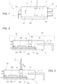
- the pillar is embedded in the housing 2 so that its lateral sides are completely or almost completely surrounded by and in contact with a packaging mass that blocks the pillar.
- Signal or power leads 4 protrude from lateral surfaces 2C of the housing 2, here two lateral surfaces 2C opposite to each other.
- the power connectors 5 (only one visible) are formed by pillars 8 attached to a substrate 10.
- a first, a second, a third and a fourth connection region 14A-14D are for example visible in Figure 2 .
- first and the second electronic components 15A, 15B for example power components such as diodes, transistors, thyristors or IGBTs, or packaged discrete components are attached and electrically coupled to the first and, respectively, to the second connection regions 14A, 14B.
- power components such as diodes, transistors, thyristors or IGBTs
- packaged discrete components are attached and electrically coupled to the first and, respectively, to the second connection regions 14A, 14B.
- the third connection region 14C is coupled to one of the leads 4, in a not visible manner and ideally represented by a dashed line 16.
- the third connection region 14C is connected in a manner not shown (for example, through wires or through tracks formed in the second conductive layer 13) to one or both the electronic components 15A, 15B.
- the leads 4 may also be connected directly to the electronic components 15A, 15B.
- the fourth connection region 14D carries and is electrically coupled to one of the pillars 8.
- the pillar 8 of Figure 2 may be soldered or glued to the fourth connection region 14D through bonding material 18, for example using a filler material or a conductive glue or adhesive.
- the pillar 8 here has a cylindrical shape with a circular base and extends from the fourth connection region 14D up to the upper surface 4A of the housing 2, perpendicular to the substrate 10.
- the pillar 8 protrudes slightly from the upper surface 4A with an end 8A.
- the pillar 8 has dimensions generally linked to the dimensions of the power module 1. For example, it may have a height comprised between 2 and 7 mm, in particular of about 4.5 mm, and a diameter comprised between 1 and 5 mm, for example of about 2 mm.
- the end 8A of the pillar 8 is flat and may be used for coupling to user boards, as represented with a dashed line in Figure 2 (board 20).
- a pin 21 may be attached to the pillar 8, as shown in Figure 3 .
- pin 21 is intended as a rod-shaped element that allows a current to flow and has a height higher than or equal to that of the pillar 8.
- the pin 21 has a base 22, wider than the rod-shaped portion, attached to the end 8A of the pillar 8.
- the base 22 may have a thickness comprised between 0.2 and 0.4 mm and a diameter comprised between 1.8 and 3 mm.
- the pins 21 may also have enlarged press-fit-type pin contact zones (not shown in Figure 2 , see Figure 15A ) in proximity to their distal end (remote from the pillar 8).
- the pins 21 may have two enlarged press-fit-type contact zones, as shown in Figure 15B and discussed below.
- the pins 21 may have stop zones, as shown in Figure 15C and discussed below.
- the pins 21 may have any base, for example square (with a side between 0.6 and 3 mm).
- the pillar 8 has a flat end 8A, substantially level with the upper surface 2A of the housing 2.
- the pin 21 is attached to the pillar 8 by soldering or gluing.
- bonding material (not shown) may be provided between the pin 21 and the pillar 8, for example soldering filler material or a conductive glue.
- the pin 21 may be press-fit to the pillar 8, as shown in Figure 15B .
- the power connectors 5 comprise a bigger area portion, referred to as pillar portion 28, similar to the pillar 8 of Figures 2, 3 , and a narrower and longer portion, here called pin portion 29, formed monolithically.
- the pillar portion 28 extends inside the housing 2 (except for a slightly protruding section) and the pin portion 29 extends from the pillar portion 28, seamlessly, externally to the housing 2.
- the pillar portion 28 is perpendicular to the upper surface 2A of the housing 2.
- the pillar 8 and the pillar portion 28 may have structures which prevent undesired extraction thereof, such as protruding portions, recessing portions, undercuts, knurls, surface irregularities and the like.
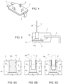
- Figure 6A shows a pillar 8 of cylindrical shape, having a peripheral groove 30 with annular shape and triangular section, intended to be filled with the resin of the housing 2 which blocks it in position.
- the groove 30 is formed at about half the height of the pillar 8 or at a midway point, but it may be arranged at any height.
- the surface of the pillar 8 may form one or more protruding annular structures, blocking the pillar 8 inside the packaging mass 3 forming the housing 2.
- Figure 6B shows a pillar 8 having the groove 30 and provided with an axial recess 31 extending from the end 8A towards the inside of the pillar 8.
- the pin 21 may be press-fit into the axial recess 31 and blocked, without the need to use glues and/or soldering.
- Figure 6C shows a pillar 8 having the groove 30 and provided with a threaded hole 33 which extends axially from the end 8A towards the inside of the pillar 8.
- the pin 21 may be screwed to the pillar 8, also here without glues and/or soldering.
- the surface of the enlarged head 31 may form knurls or protruding and/or recessing structures which block it inside the housing 2.
- Figure 7B shows a pillar 8 having the enlarged head 35 and the groove 30 as in Figure 7A , and also an axial recess 31 similar to Figure 6B . Also in this solution, therefore, the pin 21 may be press-fit into the axial recess 31.
- Figure 7C shows a pillar 8 provided with the enlarged head 35 and the groove 30 as in Figure 7A , and also with a threaded hole 33 as in Figure 6C .
- the pin 21 may be screwed to the pillar 8.
- Figures 9 and 10 show a portion of a power module 1 having power connectors 5 of the type shown in Figure 7A , with a flat end 8A, wherein the housing 2 has measures to compensate for any dimension differences with respect to design values, as well as misalignments and positioning inaccuracies due to manufacturing and/or assembling tolerances.
- the peripheral slot 38 includes an inclined surface 49 ( Figure 10 ) that is at an angle with respect to the upper surface 2A of the housing 2 and protrudes with respect thereto.
- the peripheral slot 38 here extends to a short distance from the end 8A, so that this end 8A is surrounded by an annular portion 39 of the material of the housing 2, wherein the annular portion 39 is in turn surrounded by the peripheral slot 38.
- the pillar 8 has the groove 30 near the end 8A.
- Figure 10 shows a portion of the power module 1 during molding.
- the power module 1 is inserted into a mold (represented only schematically and indicated by 43) which comprises one or more ejectors 40, one for each power connector 5.
- the head surface 41 of the ejector 40 has a central zone 41A that is plane and a peripheral zone 41B protruding with respect to the central zone 41A and forming a step 42.
- the central zone 41A (typically circular, in case of pillar 8 with a circular section) has a greater area than the end 8A of the pillar 8, so as to rest flat on this end 8A and protrude laterally thereto with the step 42 arranged to partially surround, at a distance, the end 8A of the pillar 8.
- the resin covers the support 10 and the electronic components 15A, 15B, surrounds each pillar 8 and also gets into the gap existing between the step 42 of the ejector 40 and the end 8A of the pillar 8, creating the peripheral slot 38 and the annular portion 39.
- the ejector 40 is rested on the end 8A of the pillar 8 with its central zone 41A, planar, and held in position by mechanical or pneumatic springs (not shown) capable of compensating for height errors of the end 8A of the pillar 8; the dimension of the central zone 41A allows compensation of any positioning errors along the axis X and/or the axis Y, as well as any small dimensional thickness tolerances, ensuring that the resin does not extend above the end 8A or form undesired peripheral burrs.
- Figures 11 and 12 show the step of forming the housing 2 for a power connector 5 having an integral pin portion 29.
- the ejector 40 is again hollow, to house the pin portion 29 of the power connector 5.
- the central zone 41A of the head surface 41 abuts against the shoulder formed by the enlarged head 35 of the pillar portion 28.
- Figure 15A shows a solution wherein the pins 21 are attached to the pillars 8 through so-called pin holders 45 and have an end 21A having an enlarged zone (for example formed by axial bumps) so as to allow a press-fit connection with a connection support, such as a printed circuit board PCB.
- a connection support such as a printed circuit board PCB.
- each pin holder 45 is formed by a tubular body 46, here of cylindrical shape, having a through axial cavity 47 and provided, on one of its bases, with a flange 48.
- the pins 21 are then each interference-fit into a respective pin holder 45.
- Figure 15B shows a pin 21 having two enlarged ends 21A, 21B, for press-fit connection.
- the pin 21 of Figure 15B may be connected, with one of the two enlarged ends 21A, 21B, here a first enlarged end 21A, to the pillar 8 (as shown by the arrow) and with the other of the two enlarged ends 21A, 21B, for example a second enlarged end 21B, to a support such as a PCB.
- the power module 100 comprises a housing 102 formed by two half-shells (first half-shell 101A, second half-shell 101B) of insulating material, for example plastic.
- a gel material 104 is contained inside the half-shells 101A, 101B and blocks the support 10 and the electronic components (not visible in Figure 18 ) in position.
- the support 10 is attached to the first half-shell 101A and the power connector 5 extends through a hole 106 in the second half-shell 101B.
- the power connector 5 shown in Figure 18 is formed by the pillar 8 in the configuration shown in Figures 2 and 3 ; however, it may also be provided in any of the configurations of Figures 4-17 and, in particular, may comprise a pillar portion 28 and a pin portion 29, monolithic to each other, as in Figure 5 or 8 , or comprise a pin holder, similar to the component 45 of Figures 15-17 .
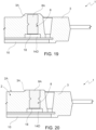
- Figures 19 and 20 show two manufacturing steps of the power module 1, according to an embodiment; here, the pillar 8 of Figure 6A is used.
- the mold (not shown) is such that the packaging mass 3 covers the end 8A of the pillar 8 and forms a protruding portion 3A.
- the protruding portion 3A is then thinned to expose the pillar 8 and the pillar 8 is shortened by a grinding operation.
- Figures 21 and 22 show two different manufacturing steps of the power module 1, according to a different embodiment; here, the pillar 8 of Figure 6A is used.
- the mold is such that the packaging mass 3 covers the end 8A of the pillar 8 without forming protruding portions.
- the packaging mass 3 has a flat upper surface 3B.
- the packaging mass 3 is then ground, from the flat upper surface 3B, to expose the pillar 8; then the upper portion of the pillar 8 and the upper portion of the packaging mass 3 are ground, so that the end 8A of the pillar 8 is flush with the packaging mass 3 ( Figure 22 ).
- Figures 23 and 24 show two different manufacturing steps of power module 1, according to an another embodiment; here, holed pillars, such as pillars 8 of Figures 6B, 6C , 7B, 7C , 15B , are used.
- the pillar 8 is soldered or glued to the fourth connection region 14D turned upside down, so that the axial recess 31 or threaded hole 33 faces the substrate 10 and a closed base 50 of the axial recess 31 or threaded hole 33 is arranged far from the substrate 10. Bonding material 18 is used.
- the packaging mass 3 has already been molded and covers the closed base 50 of the pillar 8.
- the mold (not shown) is such that the packaging mass 3 completely covers the pillar 8.
- the packaging mass 3 covers the closed base 50 of the pillar 8 and forms the protruding portion 3A.
- the packaging mass 3 and the pillar 8 are ground until completely removing the closed base 50 and form the end 8A of the pillar 8.
- the axial recess 31 or threaded hole 33 is open to the outside and the end 8A of the pillar 8 is flush with the packaging mass 3.
- the solution is easily adaptable to pins of different type and to the desired bonding type (press-fit, soldering/welding).
- the power connectors 5 are inexpensive and the assembling operations are simple, so that the power module 1, 100 has costs comparable with the known solutions.
- thinning of the packaging mass 3 and shortening of the pillar 8 may be done by any other technique allowing removal of material, for example milling.
- Thinning of the packaging mass 3 may stop at the pillar 8, without shortening the latter.
- Example 2 The power module according to example 1, wherein the electrical connector (5) comprises a pillar element (8; 28) having one end (8A) facing the main surface (2A) of the housing.
- Example 3 The power module according to the preceding example, wherein the pillar element (8; 28) has a solid cylindrical shape.
- Example 4 The power module according to the preceding example, wherein the electrical connector (5) further comprises a rod-shaped element (21) soldered to the end (8A) of the pillar element (8) and extending from the main surface (2A) of the housing (2; 102) to the outside of the housing, in prosecution of the pillar element (8).
- the electrical connector (5) further comprises a rod-shaped element (21) soldered to the end (8A) of the pillar element (8) and extending from the main surface (2A) of the housing (2; 102) to the outside of the housing, in prosecution of the pillar element (8).
- Example 5 The power module according to example 2 or 3, wherein the electrical connector (5) further comprises a pin holder (45) formed by an axially holed cylindrical body and provided with a flange end (48), the flange end being attached to the end (8A) of the pillar element (8) and extending from the main surface (2A) of the housing (2; 102) towards the outside thereof, in continuation of the pillar element (8).
- a pin holder (45) formed by an axially holed cylindrical body and provided with a flange end (48), the flange end being attached to the end (8A) of the pillar element (8) and extending from the main surface (2A) of the housing (2; 102) towards the outside thereof, in continuation of the pillar element (8).
- Example 6 The power module according to the preceding example, wherein the electrical connector (5) further comprises a rod-shaped element (21) press-fit in the pin holder (45).
- Example 7 The power module according to example 2, wherein the pillar element (8) has a cylindrical shape and comprises an axial hole (31).
- Example 8 The power module according to the preceding example, wherein the electrical connector (5) further comprises a rod-shaped element (21) press-fit or screwed into the axial hole (31) and extending in prosecution of the pillar element (8).
- Example 9 The power module according to example 2 or 3, wherein the electrical connector (5) further comprises a pin portion (29) monolithic with the pillar element (28), the pin portion (29) being rod-shaped and extending externally to the housing (2; 102) in prosecution of the pillar element (28).
- Example 10 The power module according to any of examples 2-9, wherein the pillar element (8; 28) has anti-extraction characteristics (30; 35), the anti-extraction characteristics comprising protruding and/or recessing structures (21A) and possibly stops (15).
- Example 11 The power module according to any of examples 2-10, wherein the housing (2) comprises a packaging mass (3) that is electrically insulating and forms the upper surface (2A) and the lateral surfaces (2C), wherein a recess (38) in the upper surface surrounds the end (8A) of the pillar element (8; 28).
- the housing (2) comprises a packaging mass (3) that is electrically insulating and forms the upper surface (2A) and the lateral surfaces (2C), wherein a recess (38) in the upper surface surrounds the end (8A) of the pillar element (8; 28).
- Example 12 The power module according to any of examples 2-10, wherein the housing (102) comprises a box housing an insulating gel (104) and forms a gel-potted package, wherein the box comprises a hole (106) configured to allow the end (8A) of the pillar element (8) to pass through.
- the housing (102) comprises a box housing an insulating gel (104) and forms a gel-potted package, wherein the box comprises a hole (106) configured to allow the end (8A) of the pillar element (8) to pass through.
- Example 13 The power module according to any of the preceding examples, wherein the electronic component (15A) forms a first electronic component and the housing (2; 102) houses a second electronic component (15B), the power module further comprising electrical leads (4) extending from or on the lateral surfaces (3C) of the housing and electrically coupled to external connection regions (14C) formed by the carrying substrate (10) and electrically coupled to the first and/or the second electronic component (15A, 15B).
- Example 14 An assembling method for a power module, comprising:
- Example 15 The assembling method according to the preceding example, wherein forming a housing (2) comprises molding packaging insulating material (3) with a mold (43) including an ejector (40) having a head surface (41), wherein the head surface (41) of the ejector has a central zone (41A) configured to abut against the electrical connector (5), and a peripheral zone (41B), of a greater area than the central zone (41A) and the electrical connector (5) and configured to be arranged laterally to the electrical connector (5).
- a mold (43) including an ejector (40) having a head surface (41), wherein the head surface (41) of the ejector has a central zone (41A) configured to abut against the electrical connector (5), and a peripheral zone (41B), of a greater area than the central zone (41A) and the electrical connector (5) and configured to be arranged laterally to the electrical connector (5).
Applications Claiming Priority (1)
| Application Number | Priority Date | Filing Date | Title |
|---|---|---|---|
| IT202200006617 | 2022-04-04 |
Publications (1)
| Publication Number | Publication Date |
|---|---|
| EP4258832A1 true EP4258832A1 (de) | 2023-10-11 |
Family
ID=82019944
Family Applications (1)
| Application Number | Title | Priority Date | Filing Date |
|---|---|---|---|
| EP23164244.8A Pending EP4258832A1 (de) | 2022-04-04 | 2023-03-27 | Leistungsmodul mit leiterrahmenlosen signalverbindern, insbesondere für automobilanwendungen, und montageverfahren dafür |
Country Status (3)
| Country | Link |
|---|---|
| US (1) | US20230317537A1 (de) |
| EP (1) | EP4258832A1 (de) |
| CN (2) | CN220383331U (de) |
Citations (6)
| Publication number | Priority date | Publication date | Assignee | Title |
|---|---|---|---|---|
| EP1121009A2 (de) * | 2000-01-28 | 2001-08-01 | Kabushiki Kaisha Toshiba | Halbleitende Baugruppe für Stromrichter-Einheiten mit Verkleinerungsanforderungen |
| US20090213553A1 (en) * | 2008-02-27 | 2009-08-27 | Infineon Technologies Ag | Power Module |
| US20100013086A1 (en) * | 2008-07-18 | 2010-01-21 | Mitsubishi Electric Corporation | Power semiconductor device |
| JP2012004226A (ja) * | 2010-06-15 | 2012-01-05 | Mitsubishi Electric Corp | 電力用半導体装置 |
| DE102014211698A1 (de) * | 2014-06-18 | 2015-12-24 | Robert Bosch Gmbh | Elektronisches Modul mit einer Kontakthülse |
| US20160247735A1 (en) * | 2015-02-19 | 2016-08-25 | Semiconductor Components Industries, Llc | Semiconductor package with elastic coupler and related methods |
-
2023
- 2023-03-27 EP EP23164244.8A patent/EP4258832A1/de active Pending
- 2023-03-30 US US18/193,095 patent/US20230317537A1/en active Pending
- 2023-04-03 CN CN202320711779.2U patent/CN220383331U/zh active Active
- 2023-04-03 CN CN202310346622.9A patent/CN116896835A/zh active Pending
Patent Citations (6)
| Publication number | Priority date | Publication date | Assignee | Title |
|---|---|---|---|---|
| EP1121009A2 (de) * | 2000-01-28 | 2001-08-01 | Kabushiki Kaisha Toshiba | Halbleitende Baugruppe für Stromrichter-Einheiten mit Verkleinerungsanforderungen |
| US20090213553A1 (en) * | 2008-02-27 | 2009-08-27 | Infineon Technologies Ag | Power Module |
| US20100013086A1 (en) * | 2008-07-18 | 2010-01-21 | Mitsubishi Electric Corporation | Power semiconductor device |
| JP2012004226A (ja) * | 2010-06-15 | 2012-01-05 | Mitsubishi Electric Corp | 電力用半導体装置 |
| DE102014211698A1 (de) * | 2014-06-18 | 2015-12-24 | Robert Bosch Gmbh | Elektronisches Modul mit einer Kontakthülse |
| US20160247735A1 (en) * | 2015-02-19 | 2016-08-25 | Semiconductor Components Industries, Llc | Semiconductor package with elastic coupler and related methods |
Also Published As
| Publication number | Publication date |
|---|---|
| CN220383331U (zh) | 2024-01-23 |
| US20230317537A1 (en) | 2023-10-05 |
| CN116896835A (zh) | 2023-10-17 |
Similar Documents
| Publication | Publication Date | Title |
|---|---|---|
| US7706146B2 (en) | Power system module and method of fabricating the same | |
| KR100566046B1 (ko) | 파워 반도체장치 | |
| US7944042B2 (en) | Semiconductor device and method of manufacturing same | |
| US5521437A (en) | Semiconductor power module having an improved composite board and method of fabricating the same | |
| JP3357220B2 (ja) | 半導体装置 | |
| JP6004001B2 (ja) | 半導体装置 | |
| US6710455B2 (en) | Electronic component with at least two stacked semiconductor chips and method for fabricating the electronic component | |
| EP2747137B1 (de) | Halbleitermodul | |
| JP2003031765A (ja) | パワーモジュールおよびインバータ | |
| US8174097B2 (en) | Electric sub-assembly | |
| CN108496249B (zh) | 半导体装置 | |
| EP4258832A1 (de) | Leistungsmodul mit leiterrahmenlosen signalverbindern, insbesondere für automobilanwendungen, und montageverfahren dafür | |
| US8174834B2 (en) | Molded housing used in force fit method | |
| CN116130474A (zh) | 半导体装置 | |
| JP6236547B1 (ja) | 半導体装置及び半導体装置の製造方法 | |
| JP6240343B1 (ja) | 半導体装置及び半導体装置の製造方法 | |
| JPH11220074A (ja) | 半導体装置 | |
| JP3447385B2 (ja) | ハイブリッドicおよびその製造方法 | |
| US20230187320A1 (en) | Semiconductor module | |
| WO2023189265A1 (ja) | 半導体モジュール | |
| WO2023157482A1 (ja) | 半導体モジュール、半導体装置、及び半導体装置の製造方法 | |
| WO2023189266A1 (ja) | 金属配線板 | |
| CN116469874A (zh) | 半导体装置 | |
| JPH06132472A (ja) | Icパッケージ | |
| JP2013065616A (ja) | 回路モジュール及び回路モジュールの製造方法 |
Legal Events
| Date | Code | Title | Description |
|---|---|---|---|
| PUAI | Public reference made under article 153(3) epc to a published international application that has entered the european phase |
Free format text: ORIGINAL CODE: 0009012 |
|
| STAA | Information on the status of an ep patent application or granted ep patent |
Free format text: STATUS: THE APPLICATION HAS BEEN PUBLISHED |
|
| AK | Designated contracting states |
Kind code of ref document: A1 Designated state(s): AL AT BE BG CH CY CZ DE DK EE ES FI FR GB GR HR HU IE IS IT LI LT LU LV MC ME MK MT NL NO PL PT RO RS SE SI SK SM TR |
|
| STAA | Information on the status of an ep patent application or granted ep patent |
Free format text: STATUS: REQUEST FOR EXAMINATION WAS MADE |