EP4257938A1 - Selbstausrichtende optische akustische sensoren - Google Patents
Selbstausrichtende optische akustische sensoren Download PDFInfo
- Publication number
- EP4257938A1 EP4257938A1 EP23166875.7A EP23166875A EP4257938A1 EP 4257938 A1 EP4257938 A1 EP 4257938A1 EP 23166875 A EP23166875 A EP 23166875A EP 4257938 A1 EP4257938 A1 EP 4257938A1
- Authority
- EP
- European Patent Office
- Prior art keywords
- substrate
- alignment
- diaphragm
- optical waveguide
- acoustic sensor
- Prior art date
- Legal status (The legal status is an assumption and is not a legal conclusion. Google has not performed a legal analysis and makes no representation as to the accuracy of the status listed.)
- Granted
Links
Images







Classifications
-
- G—PHYSICS
- G01—MEASURING; TESTING
- G01H—MEASUREMENT OF MECHANICAL VIBRATIONS OR ULTRASONIC, SONIC OR INFRASONIC WAVES
- G01H9/00—Measuring mechanical vibrations or ultrasonic, sonic or infrasonic waves by using radiation-sensitive means, e.g. optical means
- G01H9/004—Measuring mechanical vibrations or ultrasonic, sonic or infrasonic waves by using radiation-sensitive means, e.g. optical means using fibre optic sensors
-
- G—PHYSICS
- G01—MEASURING; TESTING
- G01H—MEASUREMENT OF MECHANICAL VIBRATIONS OR ULTRASONIC, SONIC OR INFRASONIC WAVES
- G01H9/00—Measuring mechanical vibrations or ultrasonic, sonic or infrasonic waves by using radiation-sensitive means, e.g. optical means
- G01H9/004—Measuring mechanical vibrations or ultrasonic, sonic or infrasonic waves by using radiation-sensitive means, e.g. optical means using fibre optic sensors
- G01H9/006—Measuring mechanical vibrations or ultrasonic, sonic or infrasonic waves by using radiation-sensitive means, e.g. optical means using fibre optic sensors the vibrations causing a variation in the relative position of the end of a fibre and another element
-
- G—PHYSICS
- G02—OPTICS
- G02B—OPTICAL ELEMENTS, SYSTEMS OR APPARATUS
- G02B6/00—Light guides; Structural details of arrangements comprising light guides and other optical elements, e.g. couplings
- G02B6/24—Coupling light guides
- G02B6/42—Coupling light guides with opto-electronic elements
- G02B6/4201—Packages, e.g. shape, construction, internal or external details
- G02B6/4204—Packages, e.g. shape, construction, internal or external details the coupling comprising intermediate optical elements, e.g. lenses, holograms
- G02B6/4214—Packages, e.g. shape, construction, internal or external details the coupling comprising intermediate optical elements, e.g. lenses, holograms the intermediate optical element having redirecting reflective means, e.g. mirrors, prisms for deflecting the radiation from horizontal to down- or upward direction toward a device
-
- G—PHYSICS
- G02—OPTICS
- G02B—OPTICAL ELEMENTS, SYSTEMS OR APPARATUS
- G02B6/00—Light guides; Structural details of arrangements comprising light guides and other optical elements, e.g. couplings
- G02B6/24—Coupling light guides
- G02B6/42—Coupling light guides with opto-electronic elements
- G02B6/4201—Packages, e.g. shape, construction, internal or external details
- G02B6/4219—Mechanical fixtures for holding or positioning the elements relative to each other in the couplings; Alignment methods for the elements, e.g. measuring or observing methods especially used therefor
- G02B6/4228—Passive alignment, i.e. without a detection of the degree of coupling or the position of the elements
- G02B6/423—Passive alignment, i.e. without a detection of the degree of coupling or the position of the elements using guiding surfaces for the alignment
-
- G—PHYSICS
- G02—OPTICS
- G02B—OPTICAL ELEMENTS, SYSTEMS OR APPARATUS
- G02B6/00—Light guides; Structural details of arrangements comprising light guides and other optical elements, e.g. couplings
- G02B6/24—Coupling light guides
- G02B6/42—Coupling light guides with opto-electronic elements
- G02B6/4201—Packages, e.g. shape, construction, internal or external details
- G02B6/4219—Mechanical fixtures for holding or positioning the elements relative to each other in the couplings; Alignment methods for the elements, e.g. measuring or observing methods especially used therefor
- G02B6/4236—Fixing or mounting methods of the aligned elements
- G02B6/424—Mounting of the optical light guide
-
- G—PHYSICS
- G02—OPTICS
- G02B—OPTICAL ELEMENTS, SYSTEMS OR APPARATUS
- G02B6/00—Light guides; Structural details of arrangements comprising light guides and other optical elements, e.g. couplings
- G02B6/24—Coupling light guides
- G02B6/42—Coupling light guides with opto-electronic elements
- G02B6/4201—Packages, e.g. shape, construction, internal or external details
- G02B6/4219—Mechanical fixtures for holding or positioning the elements relative to each other in the couplings; Alignment methods for the elements, e.g. measuring or observing methods especially used therefor
- G02B6/4236—Fixing or mounting methods of the aligned elements
- G02B6/4245—Mounting of the opto-electronic elements
-
- G—PHYSICS
- G01—MEASURING; TESTING
- G01V—GEOPHYSICS; GRAVITATIONAL MEASUREMENTS; DETECTING MASSES OR OBJECTS; TAGS
- G01V1/00—Seismology; Seismic or acoustic prospecting or detecting
- G01V1/22—Transmitting seismic signals to recording or processing apparatus
- G01V1/226—Optoseismic systems
Definitions
- This application relates generally to fiber-optic-based sensors and methods of fabrication, including but not limited to acoustic sensors, inertial sensors, and/or force sensors.
- Micro-electromechanical systems (MEMS) and sensors technologies are used in a wide range of applications from optical displays and switches (see, e.g., P.F. Van Kessel et al., "A MEMS-based projection display,” Proc. IEEE, vol. 86, no. 8, 1687-1704 (1998 ); C.R. Giles et al., "A silicon MEMS optical switch attenuator and its use in lightwave subsystems," IEEE J. Sel. Topics in Quant. Electr., vol. 5, no. 1,18-25 (1999 )), to pressure (see, e.g., O.N. Tufte et al., "Silicon diffused-element piezoresistive diaphragms," J.
- optical readout techniques have been integrated with microfabricated mechanical structures, such as diaphragms and mass-spring micro-system, to bridge this resolution gap (see, e.g., B.H. Afshar and M.J.F. Digonnet, "Spring-loaded diaphragm-based fiber acoustic sensor,” J. of Lightwave Technol., vol. 45, no. 14, 3933-3936 (2020 ); W. Jo et al., “Highly sensitive phase-front-modulation fiber acoustic sensor,” J. of Lightwave Technol., vol. 33, no. 20, 4377-4383 (2015 ); W.
- the probe-light frequency can be locked to the resonance frequency as the latter slowly drifts due to temperature changes (e.g., using a Pound Drexel Hall technique) to make operation of a single FP sensor more complex, and the operation of multiple FP sensors in large arrays more challenging.
- an acoustic sensor comprises at least one optical waveguide configured to emit an optical beam.
- the acoustic sensor further comprises a substantially planar first substrate optically coupled to the at least one optical waveguide.
- the first substrate is configured to be illuminated by the optical beam and to reflect at least a portion of the optical beam to the at least one optical waveguide.
- the first substrate comprises a first substrate portion configured to reflect a first portion of the optical beam back to the at least one optical waveguide.
- the first substrate further comprises a diaphragm configured to reflect a second portion of the optical beam back to the at least one optical waveguide. The diaphragm is responsive to a perturbation by moving relative to the first substrate portion.
- a method of fabricating an acoustic sensor comprises fabricating a substantially planar first substrate comprising a first substrate portion and a diaphragm.
- the diaphragm is configured to move relative to the first substrate portion in response to an acoustic perturbation.
- the method further comprises fabricating a substantially planar second substrate.
- the second substrate comprises a feedthrough hole and a plurality of orifices configured to allow a fluid medium to flow out from a region between the first substrate and the second substrate during operation of the acoustic sensor.
- the method further comprises aligning the first substrate and the second substrate to one another such that the feedthrough hole is aligned over a region between the first substrate portion and the diaphragm.
- the method further comprises affixing the first substrate and the second substrate to one another such that the second substrate is substantially parallel to the first substrate.
- phase-front modulation (PFM) sensors which are based on the modulation of the phase of an optical beam (see, e.g., U.S. Pat. No. 11,215,481 ; Afshar 2020) in which a single-mode fiber is a short distance (about 10-30 micrometers) from a silicon chip containing a compliant spring-loaded diaphragm suspended from a stationary substrate by cantilever springs. In the presence of an acoustic wave, the diaphragm vibrates in and out of the plane of the substrate.
- PFM phase-front modulation
- the fiber is aligned such that the optical beam is incident on the edge of the diaphragm, with half of the power incident on the diaphragm and the other half on the non-compliant adjacent substrate.
- Each portion of the optical beam power can be viewed as an arm of a two-wave Michelson interferometer.
- the diaphragm vibrates relative to the adjacent substrate, which modulates the phase of the reflected beam. Consequently, the percentage of power in the reflected beam that is re-coupled into the fiber core is modulated, at the acoustic frequency.
- the amplitude and frequency of the acoustic wave can be inferred by measuring the optical power of the reflected beam.
- the interferometer can be biased at quadrature (e.g., the diaphragm can be recessed relative to the adjacent substrate by ⁇ /8, where ⁇ is the laser wavelength, resulting in a ⁇ /2 round-trip phase shift between the two arms).
- the power in the two arms of the interferometer can be substantially equal to one another (e.g., the fiber can be positioned relative to the chip such that the optical power incident on the chip is distributed equally between the diaphragm and the adjacent portion of the substrate.
- an acoustic sensor provides self-alignment of the fiber and the two-wave interferometer using a precise, repeatable and scalable structure.
- the fiber alignment is integrated into the micro-fabrication process.
- an optical chip houses the optical fiber and a mechanical chip comprises the diaphragm, the optical and mechanical chips fabricated with a set of complementary mating structures (e.g., protrusions; recesses) that, when mated, position the two chips relative to one another such that the fiber is positioned precisely at the boundary between the diaphragm and the substrate.
- the first substrate 100 is substantially planar (e.g., wafer; chip) and is placed a short, non-critical distance (e.g., 10 micrometers - 100 micrometers) from the end of the optical fiber of the at least one optical waveguide 20.
- the first substrate 100 comprises at least one of the following materials: silicon, silicon nitride, silicon carbide, graphite, graphene. At least one of the first substrate portion 32 and the diaphragm 34 can be optically reflective.
- a perimeter of the diaphragm 34 is substantially surrounded by the first substrate portion 32.
- the diaphragm 34 can be within a well microfabricated into the first substrate 100 (e.g., at a depth h 0 below the surface of the first substrate portion 32).
- the first substrate 100 further comprises a plurality of cantilever springs 54 (e.g., 2, 3, 5, 6, 7, 8, 9, 10, or more) that is mechanically coupled to the diaphragm 34 such that the diaphragm 34 is elastically movable relative to the first substrate portion 32 in a direction substantially perpendicular to the diaphragm 34 in response to the perturbation.
- the diaphragm 34 can be substantially circular with substantially identical cantilever springs 54 extending radially outward from the diaphragm 34, the cantilever springs 54 suspending the diaphragm 34 from the substrate 100.
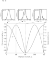
- FIG. 1B shows plots of the optical power recoupling of a reflected portion of the optical beam 22 from the first substrate 100 and an optical sensitivity of the acoustic sensor 10 as functions of the step height h 0 in accordance with certain implementations described herein.
- the optical beam 22 emerging from the end of the optical waveguide 20 is incident on the edge of the diaphragm 34, with equal portions of its intensity distributed between the diaphragm 34 and the non-compliant, adjacent first substrate portion 32.
- the portion of the optical beam 22 reflected from the diaphragm 34 accumulates an additional ⁇ round-trip phase shift relative to the portion of the optical beam 22 reflected from the adjacent first substrate portion 32.
- the reflected field profile at the end of the optical waveguide 20 (e.g., calculated by diffraction theory) is no longer a fundamental TEM 00 mode but has a two-lobed symmetrical amplitude profile (see, solid curve in the top, right plot of FIG.
- the acoustic sensor 10 is a two-wave interferometer, similar to a Michelson interferometer, where the two portions of the intensity illuminating the diaphragm 34 and the adjacent first substrate portion 32 comprise each arm of the interferometer.
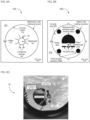
- FIGs. 2A and 2B schematically illustrate top views of an example first substrate 100 and an example second substrate 200, respectively, in accordance with certain implementations described herein.
- the first substrate 100 is substantially planar (e.g., wafer; chip)
- the second substrate 200 is substantially planar (e.g., wafer; chip)
- the second substrate 200 is configured to be bonded to the first substrate 100 such that the second substrate 200 is substantially parallel to the first substrate 100.
- FIG. 2C is a photograph of an example acoustic sensor 10 comprising an example first substrate 100 and an example second substrate 200 bonded together in accordance with certain implementations described herein.
- FIGs. 2D and 2E schematically illustrate perspective cross-sectional views of the example first substrate 100 and an example second substrate 200, respectively, of FIG.
- the second substrate 200 comprises an optical fiber feedthrough hole 210 extending through the second substrate 200 and configured to receive the optical waveguide 20 (e.g., single-mode fiber).
- the optical waveguide 20 can be fixed within the optical feedthrough hole 210 by adhesive (e.g., epoxy) such that after the first substrate 100 and the second substrate 200 are affixed together, an end of the optical waveguide 20 is spaced (e.g., by about 10 micrometers) from the first substrate 100 and positioned such that light emitted from the end of the optical waveguide 20 propagates substantially perpendicularly to the first substrate 100 and light reflected from the diaphragm 34 and the adjacent first substrate portion 32 propagates substantially perpendicularly to the first substrate 100 back to the end of the optical waveguide 20.
- adhesive e.g., epoxy
- the at least one alignment island 110 is configured to fit within the at least one alignment well 220 (e.g., analogous to LEGO ® pieces) to fix (e.g., self-align) the relative positions of the diaphragm 34 of the first substrate 100 and the feedthrough hole 210 of the second substrate 200 (e.g., a center of the feedthrough hole 210 is aligned with an edge of the diaphragm 34). While FIGs. 1A , 2A , 2B , 2D, and 2E shown an alignment island 110 and an alignment well 220 that are substantially circular, other shapes (e.g., oval; square; polygonal; irregular) are also compatible with certain implementations described herein.
- FIGs. 1A , 2A , 2B , 2D, and 2E shown an alignment island 110 and an alignment well 220 that are substantially circular, other shapes (e.g., oval; square; polygonal; irregular) are also compatible with certain implementations described herein.
- the perimeter of the at least one alignment island 110 has a step edge such that the at least one alignment island 110 has a height above a surface of a region 120 of the first substrate 100 substantially surrounding the at least one alignment island 110 and the perimeter of the at least one alignment well 220 has a depth below a surface of a region 230 of the second substrate 200 substantially surrounding the at least one alignment well 220.
- the width (e.g., diameter) of the at least one alignment island 110 has a first width that is less than a second width of the at least one alignment well 220.
- the height can be less than the depth (e.g., by about 100 micrometers) and the first width can be less than the second width (e.g., by about 5 micrometers to 8 micrometers) such that the top surface of the at least one alignment island 110 does not contact the top surface of the at least one alignment well 220 when the first substrate 100 is mated with the second substrate 200 (e.g., the surface of the region 120 of the first substrate 100 affixed to the surface of the region 230 of the second substrate 200) and the at least one alignment island 110 is tightly fit into the at least one alignment well 220.
- the second substrate 200 e.g., the surface of the region 120 of the first substrate 100 affixed to the surface of the region 230 of the second substrate 200
- the at least one alignment island 110 comprises at least one alignment ledge 112 extending from a perimeter of the at least one alignment island 110 and the at least one alignment well 220 comprises at least one alignment notch 222 extending from a perimeter of the at least one alignment well 220. While FIGs. 1A , 2A , and 2D show the alignment island 110 having a single substantially rectangular alignment ledge 112 extending substantially perpendicularly to the perimeter of the alignment island 110 and FIGs.
- the at least one alignment ledge 112 can be tightly fit within the at least one alignment notch 222.
- the at least one alignment notch 222 can provide a sufficiently precise fit (e.g., allowing only 1.5 micrometers of misplacement) to provide a sufficiently precise alignment between the center of the feedthrough hole 210 and the edge of the diaphragm 34.
- the at least one alignment ledge 112 and the at least one alignment notch 222 can provide redundancy to account for small variations in fabricated dimensions. For example, as shown in FIGs.
- the at least one alignment ledge 112 can comprise a single ledge 112 extending from the alignment island 110 and the at least one alignment notch 222 can comprises four notches 222 arranged equidistantly along and extending from the perimeter of the alignment well 220, such that the first substrate 100 of FIGs. 2A and 2D can be rotated by 90-degree increments to be fitted to the second substrate 200 of FIGs. 2B and 2E , respectively, until a minimum misalignment between the center of the feedthrough hole 210 and the edge of the diaphragm 34 amongst the four possible orientations is achieved. Owing to small variations in fabricated dimensions, not all four orientations provide the same alignment precision.
- the squeezed-film damping relief window 240a can have a substantially semicircular shape positioned over a majority of the diaphragm 34 and the fluid escape windows 240b can comprise multiple (e.g., two; four) substantially symmetrically placed substantially circular windows that are configured to provide additional fluid escape routes.
- the acoustic sensor 10 can be submerged underwater to be utilized as a hydrophone, without trapping small air pockets within the region between the first substrate 100 and the second substrate 200.
- the second substrate 200 further comprises one or more trenches 250.
- the one or more trenches 250 of FIG. 2B include a set of horizontal and curved trenches 250 in proximity to the feedthrough hole 210 and on an opposite side of the feedthrough hole 210 from the squeezed-film damping relief window 240a. Etching of the one or more trenches 250 during the fabrication process can facilitate a symmetric and vertical etch profile for the feedthrough hole 210.
- FIG. 3 schematically illustrates an example fabrication process of a first substrate 100 in accordance with certain embodiments described herein.
- This example fabrication process was used at the Stanford Nanofabrication Facility to fabricate 88 first substrates 100 concurrently on a 4-inch silicon-on-insulator wafer with a 5-micrometer optically flat device layer, a 1-micrometer box layer, and a 500-micrometer substrate layer.
- the fabrication process of the first substrate 100 involves two steps of device thinning by thermal oxidation following a dry etching process (e.g., to define the cantilever springs 54 and to release the diaphragm 34).
- the diaphragm 34 can be fabricated on the device layer first by thinning it to a thickness of 6.5 micrometers using thermal oxidation. Local oxidation of silicon (LOCOS) can then be used to create the ⁇ /8 distance between the first substrate portion 32 and the diaphragm 34.
- LOC Local oxidation of silicon
- DRIE deep reactive ion etch
- the shape of the diaphragm 34 and the alignment island 110 can be etched on the device layer.
- the wafer can then be flipped, and the diaphragm 34, suspended on the SiO 2 box layer, can be exposed from the substrate layer using another DRIE step.
- the box layer can then be removed by vapor hydrofluoric acid to fully release the diaphragm 34.
- the device layer can be coated with a 7-nanometer-thick chromium adhesion layer, and a 40-nanometer-thick gold layer to increase its power reflectivity to a measured value of about 70%.
- the completed wafer can contain multiple first substrates 100 each with a single diaphragm 34 with dimensions summarized in Table 1: Parameter Design value Diaphragm radius ( a ) 500, 1000, or 1500 micrometers Cantilever length ( L ) 400 or 600 micrometers Number of cantilevers ( n ) 8 Young's modulus of Si ( E ) 169 GPa Cantilever width ( w ) 15 micrometers Cantilever height ( h ) 5 micrometers
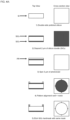
- FIGs. 4A-4C schematically illustrate top views and cross section view of an example second substrate 200 at various stages of an example fabrication process in accordance with certain embodiments described herein.
- This example fabrication process was also used at the Stanford Nanofabrication Facility on a standard 500-micrometer thick, 4-inch silicon wafer to fabricate 88 second substrates 200 concurrently.
- Plasma enhanced chemical deposition can be used to deposit 2 micrometers of silicon dioxide hard-mask on both surfaces of the Si wafer and a 3-micrometer-thick layer of photoresist (PR) can be spun on the top SiO 2 surface of the Si wafer.
- PR photoresist
- Structures corresponding to an alignment well 220 with four substantially rectangular alignment notches 222 can be exposed on the PR and then etched through the SiO 2 hard-mask (e.g., with a magnetically-enhanced reactive ion etcher (MERIE)).
- the exposed regions of the Si wafer, in the shape of the alignment well 220 and the four alignment notches can be etched using DRIE to a depth of 100 micrometers.
- the Si wafer can be flipped over and attached to a support wafer (e.g., using Crystalbond TM adhesive), and a 7-micrometer-thick layer of PR can be spun on its backside.
- the PR can be exposed with a pattern including the feedthrough holes 210, squeezed-film damping relief windows 240a, and fluid escape windows 240b.
- the PR can be exposed to a pattern comprising lines (e.g., 60-micrometer wide tracks) tracing the perimeters of the windows 240a, 240b, along with the trenches 250 (e.g., at an opposite side of the feedthrough hole 210 from the squeezed-film damping relief window 240a).
- the trenches 250 are configured to substantially reduce asymmetry in the electric fields at the surface of the oxide hard-mask in the proximity of the feedthrough hole 210 that would otherwise occur during a subsequent DRIE step due to etching of the squeezed-film damping relief window 240a in close proximity to the smaller feedthrough hole 210 and fluid escape windows 240b.
- trenches 250 Without the trenches 250, such asymmetrical electric fields can adversely affect the geometry and/or orientation of the etched feedthrough hole 210 causing imprecision in the resulting position and/or orientation of the optical waveguide 20 within the feedthrough hole 210.
- certain implementations facilitate a symmetrical charge build up on the oxide hard-mask surface in the proximity of the feedthrough hole 210 during the subsequent DRIE step.
- the backside SiO 2 hard-mask can be etched (e.g., using MERIE) through the SiO 2 to expose the pattern to the Si wafer.
- the feedthrough hole 210 and the other structures of the pattern can then be etched (e.g., using DRIE) all the way through the Si wafer.
- the support wafer can be removed (e.g., by dissolving the Crystalbond TM adhesive in acetone) and the SiO 2 hard-mask can be etched away (e.g., in a 49% hydrofluoric acid solution).
- the top surface of the Si wafer can be coated with an adhesion layer of chromium (e.g., 7-nanometers thick) and then gold (e.g., 15-nanometers thick).
- the resulting second substrates 200 are configured to have precise features that complement the features of the first substrates 100.
- fabrication of the acoustic sensor 10 comprising a method of aligning and bonding the first substrate 100 and the second substrate 200 to one another to reduce (e.g., minimize) an offset (e.g., due to fabrication tolerances) between the feedthrough hole 210 and the edge of the diaphragm 24.
- the first and second substrates 100, 200 can be mounted on a flip-chip bonder.
- the method can comprise placing the first and second substrates 100, 200 in a first orientation relative to one another in which the at least one alignment ledge 112 of the first substrate 100 is substantially aligned with the at least one alignment notch 222 of the second substrate 200 (e.g., with a single alignment ledge 112 substantially aligned with a corresponding one of the four alignment notches 222 equidistant from one another around the alignment well 220).
- the method can further comprise substantially aligning a center of the feedthrough hole 210 with an edge of the diaphragm 34 while the first and second substrates 100, 200 are in a first orientation.
- the method can further comprise measuring a first offset between the center of the feedthrough hole 210 and the edge of the diaphragm 34 (e.g., using a beam splitter and microscope of the flip-chip bonder) while the first and second substrates 100, 200 are in the first orientation.
- the method can further comprise rotating one of the first and second substrates 100, 200 (e.g., by 90 degrees in the case of the single alignment ledge 112 and the four alignment notches 222) relative to the other of the first and second substrates 100, 200 such that the first and second substrates 100, 200 are in a second orientation relative to one another in which the at least one alignment ledge 112 is substantially aligned with the at least one alignment notch 222.
- the method can further comprise substantially aligning the center of the feedthrough hole 210 with the edge of the diaphragm 34 while in the second orientation.
- the method can further comprise measuring a second offset between the center of the feedthrough hole 210 and the edge of the diaphragm 34 (e.g., using a beam splitter and microscope of the flip-chip bonder) while the first and second substrates 100, 200 are in the second orientation.
- the method can further comprise further rotations to additional orientations in which the at least one alignment ledge 112 is substantially aligned with the at least one alignment notch 222, further substantial alignments of the center of the feedthrough hole 210 with the edge of the diaphragm 34 while in the additional orientations, and further measuring additional offsets between the center of the feedthrough hole 210 and the edge of the diaphragm 34 while in the additional orientations.
- the method can further comprise comparing the first, second, and any additional offsets to one another and evaluating which of the orientations has the least offset between the center of the feedthrough hole 210 and the edge of the diaphragm 34.
- the method can further comprise substantially realigning the center of the feedthrough hole 210 with the edge of the diaphragm 34 while in the orientation having the least offset.
- the method can further comprise bonding (e.g., permanently attaching) the first and second substrates 100, 200 to one another while in the orientation having the least offset (e.g., using thermo-compression bonding of gold by pressing the first and second substrates 100, 200 together with 50 N of force while heating the first and second substrates 100, 200 at 350 degrees Celsius for 4 minutes, forming a metallic bond between the two gold-coated surfaces of the first and second substrates 100, 200; see, e.g., Tsau 2004).
- bonding e.g., permanently attaching
- the first and second substrates 100, 200 to one another while in the orientation having the least offset e.g., using thermo-compression bonding of gold by pressing the first and second substrates 100, 200 together with 50 N of force while heating the first and second substrates 100, 200 at 350 degrees Celsius for 4 minutes, forming a metallic bond between the two gold-coated surfaces of the first and second substrates 100, 200; see, e.g., Tsau 2004).
- fabrication of the acoustic sensor 10 further comprises inserting an end of the optical waveguide 20 (e.g., anti-reflection coated bare fiber end of Corning SMF-28 fiber) into the feedthrough hole 210 and attaching the optical waveguide 20 to the second substrate 200.
- the bonded assembly can be laid on a flat surface with the second substrate 200 facing the optical waveguide 20 that is mounted on a three-axis micro-positioner.
- the end of the optical waveguide 20 can be aligned to the center of the feedthrough hole 210 and then lowered into the feedthrough hole 210 to an operational distance from the first substrate 100.
- the waveguide-diaphragm distance can be determined by measuring the free spectral range of the weak interferometer formed by the small reflections at the fiber interface and the strong reflections from the first substrate 100. For example, light from a broadband source (e.g., centered at a wavelength of 1.56 micrometers) can be launched into the optical waveguide 20 through a circulator and towards the first substrate 100 and the reflected light received by the optical waveguide 20 from the first substrate 100 can be redirected towards an optical spectrum analyzer.
- a broadband source e.g., centered at a wavelength of 1.56 micrometers
- the optical waveguide 20 can be bonded to the second substrate 200 (e.g., using about 0.5 ⁇ L of a UV curable epoxy).
- this subassembly can be affixed (e.g., clamped) to a housing (e.g., having a 1 cm 3 back-chamber with two small holes, one to thread the waveguide to the experimental setup and one to reduce sensitivity to static pressure).
- a housing e.g., having a 1 cm 3 back-chamber with two small holes, one to thread the waveguide to the experimental setup and one to reduce sensitivity to static pressure).
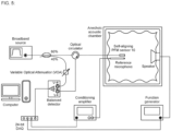
- FIG. 5 schematically illustrates an example experimental setup configured to characterize the acoustic sensitivity, noise, and resolution of an acoustic sensor.
- This example experimental setup was used to characterize acoustic sensors 10 in accordance with certain implementations described herein.
- FSS superfluorescent fiber source
- Light from the SFS was split with a 60-40 fiber coupler, 60% of the power was sent through a circulator to the acoustic sensor 10, and the remaining 40% was sent to a variable optical attenuator (VOA) then to one of the photodiodes of a balanced detector.
- VOA variable optical attenuator
- the reflected light from the acoustic sensor 10 was directed by the circulator to the second photodiode of the balanced detector.
- the VOA was adjusted until the same power was incident on both photodiodes.
- the output of the balanced detector was connected to a 24-bit data acquisition (DAQ) system, which itself was connected to a computer.
- DAQ data acquisition
- the acoustic sensor 10 was placed in an anechoic chamber to isolate the acoustic sensor 10 from laboratory noise.
- a reference microphone adjacent to the acoustic sensor 10 provided a calibrated measurement of the pressure incident on the acoustic sensor 10.
- the output of the reference microphone was connected to the DAQ system.
- the sound measured by both the acoustic sensor 10 and the reference microphone was generated by an acoustic source (e.g., speaker) mounted at the back of the anechoic chamber.
- the acoustic source was excited by a monotonic sinusoidal signal between 40 Hz to 40 kHz from a function generator controlled by the computer.
- S N the normalized acoustic sensitivity of the optical microphone, S N , at an acoustic frequency ⁇ a can be defined as the change in the power recoupled into the fiber, P c , due to a small pressure perturbation, dp , normalized to the input optical power, P in .
- This third derivative is the only term that depends on the acoustic frequency, and this term defines the shape of the acoustic sensor's spectral response.
- the optical sensitivity, S opt can be predicted theoretically using diffraction theory (see, e.g., Afshar 2020).
- the optical sensitivity, S opt is a function of (i) the optical wavelength ⁇ , (ii) the fiber-to-chip spacing z , (iii) the diaphragm step height h 0 , (iv) the lateral misalignment between the center of the beam and the edge of the diaphragm g, and (v) the angular misalignment between the fiber and the mechanical chip ⁇ tilt .
- the optical sensitivity can be calculated to be 1.94 ⁇ 10 6 m -1 (the maximum value shown in FIG. 1B ).
- the mechanical compliance C m is proportional to the surface area of the diaphragm (e.g., scaling the differential pressure p d ) and inversely proportional to the flexibility of the cantilever springs supporting the diaphragm (see, e.g., T.S.D. Senturia, "Microsystem Design," Springer, Ch. 9, 207-217 (2007 )).
- the expression for the mechanical compliance as a function of the number of cantilevers and their dimensions is provided in Afshar 2020.
- the two sensors described herein were nominally identical. Their parameters are summarized in Table 1, a diaphragm with a radius of 1500 micrometers and cantilevers with a length of 400 micrometers. Their calculated mechanical compliance C m is 178.5 nm/Pa. Their acoustic response R a ( ⁇ a ) was calculated by treating the full sensor structure including the 1-cm 3 back-chamber as a lumped acoustic circuit model (see, e.g., O.C. Akkaya et al., "Modeling and demonstration of thermally stable high-sensitivity reproducible acoustic sensors," J. Microelectromech Syst., vol. 21, no.6, 1347-1356 (2012 )).
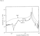
- FIG. 6 is a plot of the normalized sensitivity spectrum of an ideal sensor, calculated for these values.
- the ideal normalized sensitivity exhibits a flat-band sensitivity of 0.3 Pa -1 extending from 90 Hz to 2.4 kHz and a fundamental resonance at 3.3 kHz. Beyond the resonance, the sensitivity decreases proportional to ⁇ a -2 associated to the response of a simple harmonic oscillator past its resonance. Below 90 Hz, the sensitivity decreases proportional to ⁇ a as the vent holes at the end of the back-chamber leak pressure into the chamber and decrease p d .
- FIG. 6 also plots the normalized sensitivity S N spectra of two assembled sensors measured using the measurement setup of FIG. 5 .
- Both sensors exhibit similar sensitivity spectra spanning from 40 Hz to 10 kHz that closely match the general spectral shape of the modeled sensitivity of the ideal sensor.
- the measured flat-band sensitivity is 0.11 Pa -1 between 250 Hz and 2.3 kHz.
- the fundamental resonance of the diaphragm structure is at 3.2 kHz for sensor 1 and 2.8 kHz for sensor 2.
- Both sensors exhibit dips in sensitivity between 100 Hz and 250 Hz, which are caused by small air leaks where the bonded chip sub-assembly sits on the housing of the back-chamber. This dip in sensitivity can be avoided by improving the seal between the chips and the housing.
- the wavelength dependence of the power recoupling and normalized sensitivity were measured.
- the broadband SFS in the experimental setup of FIG. 5 was replaced with a tunable laser with a linewidth of 0.8 femtometer.
- the probing wavelength was swept from 1480 nanometers to 1580 nanometers and the average recoupled power P c then the sensitivity of sensor 1 to a 100 mPa acoustic excitation at 1 kHz was recorded.
- FIG. 7 plots the normalized sensitivity and the power recoupling coefficient of sensor 1 measured as a function of the probe wavelength.
- the measured ⁇ and S N were fitted to their respective models (see, Afshar 2020) to infer the values of five sensor parameters: (i) the diaphragm step height h 0 , (ii) the lateral misalignment between the beam and the diaphragm g, (iii) the power loss due to the angular misalignment ⁇ tilt , (iv) the fiber-to-chip spacing z , and (v) the mechanical response at 1 kHz C m ⁇ R a (1 kHz).
- the modeled values shown as dashed curves
- the measured ⁇ and S N shown as solid curves).
- the fitted parameters can be taken as a credible representation of the sensor parameters.
- the fitted parameters are reasonably close to their targeted ideal values.
- FIGs. 8A and 8B plot the noise spectral density (in W/ ⁇ Hz) of sensor 2 as a function of acoustic frequency measured at 760 Torr and 100 Torr, respectively.
- the measured noise tends to decrease from 40 Hz up to 1 kHz, then increases in four sets of resonances centered around 1.5 kHz, 3 kHz, 5.3 kHz, and 8.3 kHz.
- the individual contributions to the total noise of the sensor are detector noise, optical shot noise, thermo-mechanical noise, 1/f electronic noise and the ambient noise leaking into the chambers.
- the detector noise was measured to be 0.8 pW/ ⁇ Hz from 40 Hz to 10 kHz.
- the optical shot noise was calculated to be 7 pW/ ⁇ Hz based on an average detected power of 73 ⁇ W incident on each of the two diodes of the balanced detector.
- FIGs. 8A and 8B also plot the Euclidean sum of the shot and detector noises and a 1/f electronic noise of the detector that is manifested as 1/ ⁇ f in the plot of optical power density.
- the ambient noise leaking into the chamber is hard to incorporate as a model and inferred by comparing the measured noise of sensor 2 at the two static pressures of 760 Torr ( FIG. 8A ) and 100 Torr ( FIG. 8B ). The only other remaining noise contribution is the thermo-mechanical noise.
- thermo-mechanical noise is the stochastic vibrations of the diaphragm structure due to its thermodynamic interaction with the surrounding medium to reach thermal equilibrium (see, e.g., P. R. Saulson, "Thermal noise in mechanical experiments," Phys. Rev. D, vol. 42, no. 8, 2437-2445 (1990 )). These random diaphragm vibrations modulate the phase of light reflected from the diaphragm that result in an intensity modulation of the recoupled light into the fiber.
- a simple model of the thermo-mechanical noise can be considered where the diaphragm structure is modeled as a multi-mode harmonic oscillator with orthogonal resonant modes ⁇ i .
- the displacement mode ⁇ i is normalized such that ⁇ ⁇ i
- ⁇ j > ⁇ ij .
- the modeled thermo-mechanical noise of sensor 2 is plotted in FIGs. 8A and 8B , incorporating the first three resonances of the diaphragm structure at 2.8 kHz, 5.3 kHz, and 8.3 kHz.
- the mass of the diaphragm was calculated based on its physical dimensions.
- the displacement ratio ⁇ i for each resonance mode was modeled numerically. The only remaining unknown parameters were the damping coefficients c i .
- the damping coefficient of the fundamental resonance mode, c 1 was inferred by fitting the measured sensitivity spectrum of FIG. 6 with the model of a simple harmonic oscillator. The remaining values of c i were inferred based on the width of the subsequent resonance modes of the measured noise spectrum.
- FIGs. 8A and 8B also plot the total expected noise of sensor 2.
- the measured noise is in good agreement with the expected noise above 4.4 kHz, where it is predominantly limited by the calculated thermo-mechanical noise. Between 40 Hz to 4.4 kHz, the measured noise is on average nine times higher than the expected noise and likely dominated by ambient acoustic vibrations leaking into the chamber.
- the pressure inside the vacuum chamber was reduced to 100 Torr. Doing so reduces the transmission of the acoustic noise by the ratio of the two pressures (about 7.6) without substantially reducing damping around the spring-loaded diaphragm, which depends weakly on pressure, near atmospheric pressures (see, e.g., F. R. Blom et al, "Dependence of the quality factor of micromachined silicon beam resonators on pressure and geometry," J. Vac. Sci. Technol. B, vol. 10, no. 1, 19-26 (1992 )).
- FIG. 8B demonstrates the measured and calculated noise spectra of sensor 2 at 100 Torr to be in good agreement from 200 Hz to 10 kHz. Between 40 Hz to 2.5 kHz, the measured noise is eight times lower than the noise at 760 Torr, and the fitted damping coefficients and thermo-mechanical noise (7.5 pW/ ⁇ Hz) are within 50% of their respective values at 760 Torr (10.6 pW/ ⁇ Hz). Thus, all noises are accounted for and the sensor is ambient-noise limited at 760 Torr.
- the minimum detectable pressure (MDP), equivalent to a signal-to-noise ratio of unity, can be calculated by dividing the measured noise spectrum at 760 Torr (normalized by the input power) by the sensitivity spectrum.
- FIG. 9 plots the measured MDP of sensor 2 for an input power of 1.2 mW.
- the MDP decreases from 200 ⁇ Pa/ ⁇ Hz to 360 nPa/ ⁇ Hz between 40 Hz and 1 kHz, followed by two hikes to 6 ⁇ Pa/ ⁇ Hz between 1.2 kHz and 2.6 kHz, and increases beyond 4 kHz.
- the average measured MDP between 40 Hz and 4 kHz is 2.4 ⁇ Pa/ ⁇ Hz and the minimum measured MDP of the sensor is 260 nPa/ ⁇ Hz at 1.9 kHz and 3.7 kHz.
- the measured MDP is limited by ambient noise of the chamber and is not a true reflection of the sensor's self-noise.
- the expected MDP based on the sensor self-noise can be calculated as the ratio of the total expected noise (e.g., plotted in FIGs. 8A and 8B ) to the measured sensitivity (e.g., plotted in FIG. 6 ).
- the average expected MDP is 215 nPa/ ⁇ Hz between 40 Hz and 4 kHz reaching a minimum of 80 nPa/ ⁇ Hz at 2.6 kHz.
- the terms “generally parallel” and “substantially parallel” refer to a value, amount, or characteristic that departs from exactly parallel by ⁇ 10 degrees, by ⁇ 5 degrees, by ⁇ 2 degrees, by ⁇ 1 degree, or by ⁇ 0.1 degree
- the terms “generally perpendicular” and “substantially perpendicular” refer to a value, amount, or characteristic that departs from exactly perpendicular by ⁇ 10 degrees, by ⁇ 5 degrees, by ⁇ 2 degrees, by ⁇ 1 degree, or by ⁇ 0.1 degree.
- the ranges disclosed herein also encompass any and all overlap, sub-ranges, and combinations thereof. Language such as “up to,” “at least,” “greater than,” less than,” “between,” and the like includes the number recited.
- ordinal adjectives e.g., first, second, etc.
- the ordinal adjective are used merely as labels to distinguish one element from another (e.g., one signal from another or one circuit from one another), and the ordinal adjective is not used to denote an order of these elements or of their use.
Landscapes
- Physics & Mathematics (AREA)
- General Physics & Mathematics (AREA)
- Optics & Photonics (AREA)
- Micromachines (AREA)
Applications Claiming Priority (1)
| Application Number | Priority Date | Filing Date | Title |
|---|---|---|---|
| US202263362496P | 2022-04-05 | 2022-04-05 |
Publications (2)
| Publication Number | Publication Date |
|---|---|
| EP4257938A1 true EP4257938A1 (de) | 2023-10-11 |
| EP4257938B1 EP4257938B1 (de) | 2025-08-20 |
Family
ID=85979866
Family Applications (1)
| Application Number | Title | Priority Date | Filing Date |
|---|---|---|---|
| EP23166875.7A Active EP4257938B1 (de) | 2022-04-05 | 2023-04-05 | Selbstausrichtende optische akustische sensoren |
Country Status (2)
| Country | Link |
|---|---|
| US (1) | US12504320B2 (de) |
| EP (1) | EP4257938B1 (de) |
Citations (4)
| Publication number | Priority date | Publication date | Assignee | Title |
|---|---|---|---|---|
| US7355720B1 (en) * | 2005-12-20 | 2008-04-08 | Sandia Corporation | Optical displacement sensor |
| EP3059562A1 (de) * | 2015-02-23 | 2016-08-24 | The Board of Trustees of the Leland Stanford Junior University | Phasenfront-modulationssensor und verfahren zur herstellung |
| CN108132093B (zh) * | 2017-10-11 | 2020-08-11 | 黄辉 | 一种悬膜光纤声波传感器及其制备方法 |
| US11215481B2 (en) | 2018-03-23 | 2022-01-04 | The Board Of Trustees Of The Leland Stanford Junior University | Diaphragm-based fiber acoustic sensor |
Family Cites Families (110)
| Publication number | Priority date | Publication date | Assignee | Title |
|---|---|---|---|---|
| US2923915A (en) | 1957-01-22 | 1960-02-02 | vogel | |
| US3831137A (en) | 1972-04-14 | 1974-08-20 | Us Navy | Acousto-optic underwater detector |
| NZ186808A (en) | 1977-04-06 | 1979-10-25 | Rocol Ltd | Lubricant composition containing group ii-a metal carbonate and halogenated organic lubricant |
| GB1558689A (en) | 1977-12-06 | 1980-01-09 | Standard Telephones Cables Ltd | Reduction of reflection at fibre optic ends |
| US4446543A (en) | 1979-07-02 | 1984-05-01 | The United States Of America As Represented By The Secretary Of The Navy | Optical resonator single-mode fiber hydrophone |
| CA1123642A (en) | 1979-07-04 | 1982-05-18 | Alexander W. Lightstone | Multimode optical fiber coupler |
| CA1124384A (en) | 1979-08-09 | 1982-05-25 | Paolo G. Cielo | Stable fiber-optic hydrophone |
| JPS584322B2 (ja) | 1979-12-10 | 1983-01-26 | 日本電信電話株式会社 | 光変調装置 |
| JPS5852778B2 (ja) | 1982-06-08 | 1983-11-25 | 株式会社井上ジャパックス研究所 | 電気加工における加工液供給装置 |
| DE3271143D1 (en) | 1982-07-28 | 1986-06-19 | Maihak Ag | Process and device for an interferometric measurement of the linear displacement of an object with recognition of its direction of movement |
| JPS59155526A (ja) | 1983-02-25 | 1984-09-04 | Hitachi Ltd | デイ−ゼルエンジン排気浄化装置 |
| US4519252A (en) | 1983-03-21 | 1985-05-28 | Sperry Corporation | Pressure and temperature compensated photoelastic hydrophone |
| US4668093A (en) | 1983-06-13 | 1987-05-26 | Mcdonnell Douglas Corporation | Optical grating demodulator and sensor system |
| US5574699A (en) | 1983-10-31 | 1996-11-12 | Cuomo; Frank W. | Fiber optic lever towed array |
| SE458160B (sv) | 1984-08-09 | 1989-02-27 | Daimler Benz Ag | Foerfarande foer fiberoptisk spektralkodad oeverfoeri ng av maetvaerden och anordningar foer utoevande av foerfarandet |
| JPS6156598A (ja) | 1984-08-28 | 1986-03-22 | Oki Electric Ind Co Ltd | 光フアイバハイドロホン |
| JPS61235731A (ja) | 1985-04-11 | 1986-10-21 | Sharp Corp | 感圧素子 |
| US4933545A (en) | 1985-12-30 | 1990-06-12 | Metricor, Inc. | Optical pressure-sensing system using optical resonator cavity |
| US5052228A (en) | 1986-11-19 | 1991-10-01 | Massachusetts Institute Of Technology | Shear stress measuring device |
| US5000901A (en) | 1988-07-25 | 1991-03-19 | Abbott Laboratories | Fiber-optic physiological probes |
| US5039492A (en) | 1989-01-27 | 1991-08-13 | Metricor, Inc. | Optical pH and gas concentration sensor |
| US4911516A (en) | 1989-02-27 | 1990-03-27 | General Electric Company | Optical device with mode selecting grating |
| JPH03160774A (ja) | 1989-11-20 | 1991-07-10 | Toshiba Corp | 半導体レーザモジュール |
| US5280173A (en) | 1992-01-31 | 1994-01-18 | Brown University Research Foundation | Electric and electromagnetic field sensing system including an optical transducer |
| JPH0652073A (ja) | 1992-07-29 | 1994-02-25 | Toshiba Corp | 通信インタフェースボードのテスト装置 |
| US5311485A (en) | 1992-10-30 | 1994-05-10 | The United States Of America As Represented By The United States Department Of Energy | Fiber optic hydrophone |
| US5488504A (en) | 1993-08-20 | 1996-01-30 | Martin Marietta Corp. | Hybridized asymmetric fabry-perot quantum well light modulator |
| US6680792B2 (en) | 1994-05-05 | 2004-01-20 | Iridigm Display Corporation | Interferometric modulation of radiation |
| FR2730810B1 (fr) | 1995-02-21 | 1997-03-14 | Thomson Csf | Capteur chimique hautement selectif |
| US5832157A (en) | 1996-07-12 | 1998-11-03 | Mcdermott Technology, Inc. | Fiber optic acoustic emission sensor |
| US6281976B1 (en) | 1997-04-09 | 2001-08-28 | The Texas A&M University System | Fiber optic fiber Fabry-Perot interferometer diaphragm sensor and method of measurement |
| RU2152601C1 (ru) | 1998-06-16 | 2000-07-10 | Научный центр волоконной оптики при Институте общей физики РАН | Волоконно-оптический датчик давления (его варианты) и способ его изготовления |
| US6188644B1 (en) | 1999-05-10 | 2001-02-13 | The United States Of America As Represented By The Secretary Of The Navy | Photon transducer |
| GB9915081D0 (en) | 1999-06-28 | 1999-08-25 | Univ London | Optical fibre interferometer |
| US7167615B1 (en) | 1999-11-05 | 2007-01-23 | Board Of Regents, The University Of Texas System | Resonant waveguide-grating filters and sensors and methods for making and using same |
| US6542244B1 (en) | 1999-12-07 | 2003-04-01 | Harris Corporation | Variable sensitivity acoustic transducer |
| US6768590B2 (en) | 2000-05-19 | 2004-07-27 | Shipley Company, L.L.C. | Method of fabricating optical filters |
| DE60133970D1 (de) | 2000-06-21 | 2008-06-26 | Matsushita Electric Industrial Co Ltd | Optische Faser mit photonischer Bandlückenstruktur |
| JP4619507B2 (ja) | 2000-09-26 | 2011-01-26 | 浜松ホトニクス株式会社 | 光ファイバ結合装置、波長可変器、圧力センサ、加速度センサ及び光学装置 |
| EP1197738A1 (de) | 2000-10-18 | 2002-04-17 | Abb Research Ltd. | Anisotroper Faserlaser-Sensor mit verteilter Rückkopplung |
| US6777244B2 (en) | 2000-12-06 | 2004-08-17 | Hrl Laboratories, Llc | Compact sensor using microcavity structures |
| US7973936B2 (en) | 2001-01-30 | 2011-07-05 | Board Of Trustees Of Michigan State University | Control system and apparatus for use with ultra-fast laser |
| US6717707B2 (en) | 2001-02-21 | 2004-04-06 | Beyond 3, Inc. | Method and system for controlling resonance within a resonator-enhanced optical system |
| US7193725B2 (en) | 2001-02-21 | 2007-03-20 | Xyratex Technology Ltd. | Method and system for optical measurement via a resonator having a non-uniform phase profile |
| US6925213B2 (en) | 2001-03-09 | 2005-08-02 | University Of Cincinnati | Micromachined fiber optic sensors |
| US6574396B1 (en) | 2001-03-12 | 2003-06-03 | Lucent Technologies Inc. | Waveguide grating arrangement using a segmented reflector |
| TW574588B (en) | 2001-03-22 | 2004-02-01 | Matsushita Electric Works Ltd | Light-beam deflecting device with photonic crystal, optical switch using the same, and light-beam deflecting method |
| US6705771B2 (en) | 2001-09-26 | 2004-03-16 | Np Photonics, Inc. | Method of fusion splicing silica fiber with low-temperature multi-component glass fiber |
| JP3642570B2 (ja) | 2001-10-23 | 2005-04-27 | 株式会社東北テクノアーチ | 光干渉型マイクロ・ハイドロホン |
| JP2003185864A (ja) | 2001-12-20 | 2003-07-03 | Fujitsu Ltd | フォトニック結晶光機能素子 |
| US6816514B2 (en) | 2002-01-24 | 2004-11-09 | Np Photonics, Inc. | Rare-earth doped phosphate-glass single-mode fiber lasers |
| US6904197B2 (en) | 2002-03-04 | 2005-06-07 | Corning Incorporated | Beam bending apparatus and method of manufacture |
| EP1481270A1 (de) | 2002-03-06 | 2004-12-01 | Pirelli & C. S.p.A. | Methode zur führung elektromagnetischer strahlung, speziell in einem integrierten optischen bauteil |
| US6807342B2 (en) | 2002-03-12 | 2004-10-19 | Opticnet, Inc. | Fiber optic tunable filter using a fabry-perot resonator |
| JP3404031B2 (ja) | 2002-03-25 | 2003-05-06 | 株式会社東芝 | 集積化光合分波器 |
| US6728457B2 (en) | 2002-07-10 | 2004-04-27 | Agilent Technologies, Inc. | Waveguides in two dimensional slab photonic crystals with noncircular holes |
| US7155087B2 (en) | 2002-10-11 | 2006-12-26 | The Board Of Trustees Of The Leland Stanford Junior University | Photonic crystal reflectors/filters and displacement sensing applications |
| US7224465B2 (en) | 2002-10-15 | 2007-05-29 | University Of Maryland | Fiber tip based sensor system for measurements of pressure gradient, air particle velocity and acoustic intensity |
| KR100490754B1 (ko) | 2002-11-15 | 2005-05-24 | 한국전자통신연구원 | 파장 의존성을 조절할 수 있는 가변 감쇠기 |
| TW588162B (en) | 2003-04-21 | 2004-05-21 | Univ Nat Chiao Tung | Fiber-optic tunable filters and intensity modulators |
| KR100489810B1 (ko) | 2003-05-12 | 2005-05-17 | 한국전자통신연구원 | 전자기력에 의해 양방향으로 구동되는 파장가변 필터 |
| JP2005045463A (ja) | 2003-07-25 | 2005-02-17 | Toshiba Corp | 音響電気変換素子 |
| US7134343B2 (en) | 2003-07-25 | 2006-11-14 | Kabushiki Kaisha Toshiba | Opto-acoustoelectric device and methods for analyzing mechanical vibration and sound |
| WO2005012923A1 (ja) | 2003-08-04 | 2005-02-10 | Murata Manufacturing Co., Ltd. | 加速度センサ |
| US7330277B2 (en) | 2003-08-20 | 2008-02-12 | Xyratex Technology Limited | Resonant ellipsometer and method for determining ellipsometric parameters of a surface |
| EP1666940A4 (de) | 2003-08-29 | 2007-10-17 | Univ Kyoto | Zweidimensionaler photonischer kristall mit luftbrückenstruktur und herstellungsverfahren für den kristall |
| JP4063740B2 (ja) | 2003-08-29 | 2008-03-19 | 国立大学法人京都大学 | エアブリッジ構造を有する2次元フォトニック結晶及びその製造方法 |
| US7054011B2 (en) | 2003-09-04 | 2006-05-30 | Virginia Tech Intellectual Properties, Inc. | Optical fiber pressure and acceleration sensor fabricated on a fiber endface |
| US7283716B2 (en) | 2003-10-21 | 2007-10-16 | The Regents Of The University Of Colorado | Strain tunable, flexible photonic crystals |
| US20050169590A1 (en) | 2003-12-31 | 2005-08-04 | Crystal Fibre A/S | Liquid crystal infiltrated optical fibre, method of its production, and use thereof |
| US20050186117A1 (en) | 2004-02-19 | 2005-08-25 | Hiroyuki Uchiyama | Gas detecting method and gas sensors |
| GB2428096B (en) | 2004-03-04 | 2008-10-15 | Halliburton Energy Serv Inc | Multiple distributed force measurements |
| US7173713B2 (en) | 2004-03-04 | 2007-02-06 | Virginia Tech Intellectual Properties, Inc. | Optical fiber sensors for harsh environments |
| US20050201660A1 (en) | 2004-03-11 | 2005-09-15 | Grot Annette C. | Apparatus for single nanoparticle detection |
| US7489846B2 (en) | 2004-03-11 | 2009-02-10 | Agilent Technologies, Inc. | Photonic crystal sensors |
| JP4208754B2 (ja) | 2004-03-24 | 2009-01-14 | 株式会社リコー | 光遅延素子 |
| US7492463B2 (en) | 2004-04-15 | 2009-02-17 | Davidson Instruments Inc. | Method and apparatus for continuous readout of Fabry-Perot fiber optic sensor |
| US20050231728A1 (en) | 2004-04-15 | 2005-10-20 | Anbo Wang | Q-point stabilization for linear interferometric sensors using tunable diffraction grating |
| JP2005309295A (ja) | 2004-04-26 | 2005-11-04 | Nec Corp | 光増幅素子、光増幅装置および光増幅システム |
| CN1985235B (zh) | 2004-04-29 | 2010-09-29 | 皇家飞利浦电子股份有限公司 | 相对运动传感器 |
| AU2005245996A1 (en) | 2004-05-21 | 2005-12-01 | Atonomics A/S | Surface acoustic wave sensor comprising a hydrogel |
| BRPI0403240B1 (pt) | 2004-08-10 | 2016-02-16 | Petroleo Brasileiro Sa | transdutor óptico para medida simultânea de pressão e temperatura em poços de petróleo e método para dita medida |
| US7400797B2 (en) | 2004-10-06 | 2008-07-15 | Corning Incorporated | Transverse closed-loop resonator |
| US7190869B2 (en) | 2004-10-29 | 2007-03-13 | The Hong Kong Polytechnic University | Two-mode photonic crystal fiber and applications thereof |
| US7187816B2 (en) | 2004-12-13 | 2007-03-06 | Purdue Research Foundation | In-fiber whitelight interferometry using long-period fiber grating |
| US7689071B2 (en) | 2004-12-22 | 2010-03-30 | Opsens Inc. | Fiber optic pressure sensor for catheter use |
| WO2006083691A1 (en) | 2005-01-28 | 2006-08-10 | Honeywell International, Inc. | Hollow core fiber optical gyro |
| CA2599696C (en) | 2005-03-02 | 2014-04-01 | Fiso Technologies Inc. | Fabry-perot optical sensor and method of manufacturing the same |
| WO2006108096A2 (en) | 2005-04-06 | 2006-10-12 | President And Fellows Of Harvard College | Method and apparatus for measuring and monitoring distances, physical properties, and phase changes of light reflected from a surface based on a ring-resonator |
| WO2006119200A2 (en) | 2005-04-29 | 2006-11-09 | The Board Of Trustees Of The Leland Stanford Junior University | High-sensitivity fiber-compatible optical acoustic sensor |
| US7308163B2 (en) | 2005-05-10 | 2007-12-11 | Hewlett-Packard Development Company, L.P. | Photonic crystal system and method of controlling/detecting direction of radiation propagation using photonic crystal system |
| CA2618685C (en) | 2005-08-12 | 2015-02-03 | Fiso Technologies Inc. | Single piece fabry-perot optical sensor and method of manufacturing the same |
| JP2009516568A (ja) | 2005-11-23 | 2009-04-23 | ユニヴァーシティ オブ ワシントン | 中断される走査共振を使用する可変順次フレーミングを用いたビームの走査 |
| US7944567B2 (en) | 2005-12-05 | 2011-05-17 | Fujifilm Corporation | Semiconductor light emitting element, light source using the semiconductor light emitting element, and optical tomography imaging apparatus |
| JP2007298368A (ja) | 2006-04-28 | 2007-11-15 | Kyocera Corp | 光ファイバ圧力センサ |
| US7881565B2 (en) | 2006-05-04 | 2011-02-01 | The Board Of Trustees Of The Leland Stanford Junior University | Device and method using asymmetric optical resonances |
| US7703328B2 (en) | 2006-05-18 | 2010-04-27 | Baker Hughes Incorporated | Pressure sensor utilizing a low thermal expansion material |
| US7474823B2 (en) | 2006-10-12 | 2009-01-06 | Hewlett-Packard Development Company, L.P. | Tunable dispersion compensation |
| US7630589B2 (en) | 2007-01-09 | 2009-12-08 | The Board Of Trustees Of The Leland Stanford Junior University | Photonic crystal structure sensor |
| US7545513B2 (en) | 2007-02-05 | 2009-06-09 | Palo Alto Research Center Incorporated | Encoding optical cavity output light |
| US7483144B2 (en) | 2007-03-02 | 2009-01-27 | Honeywell International, Inc. | Apparatus and method for resonant chemical and biological sensing |
| US8166825B2 (en) | 2007-10-30 | 2012-05-01 | Tea Time Partners, L.P. | Method and apparatus for noise reduction in ultrasound detection |
| US7697798B2 (en) | 2008-02-11 | 2010-04-13 | The United States Of America As Represented By The Secretary Of The Navy | Fiber optic pressure sensors and catheters |
| JP5220923B2 (ja) | 2008-07-10 | 2013-06-26 | ノースロップ グラマン ガイダンス アンド エレクトロニクス カンパニー,インコーポレーテツド | 光ファイバ音響センサアレイ用プッシュプル二波長ファブリペロセンサ |
| US7966887B2 (en) | 2009-03-26 | 2011-06-28 | General Electric Company | High temperature optical pressure sensor and method of fabrication of the same |
| WO2011008559A1 (en) | 2009-06-29 | 2011-01-20 | University Of Massachusetts Lowell | Optical fiber pressure sensor with uniform diaphragm and method of fabricating same |
| US8094519B2 (en) | 2009-08-19 | 2012-01-10 | The United States Of America As Represented By The Secretary Of The Navy | Intensity modulated fiber optic hydrophones |
| CA3090851C (en) | 2010-03-15 | 2023-03-07 | The Board Of Trustees Of The Leland Stanford Junior University | Optical-fiber-compatible acoustic sensor |
| CA2808214C (en) | 2010-08-17 | 2016-02-23 | Foro Energy Inc. | Systems and conveyance structures for high power long distance laser transmission |
| US20150308864A1 (en) | 2014-04-24 | 2015-10-29 | Björn N. P. Paulsson | Vector Sensor for Seismic Application |
-
2023
- 2023-03-17 US US18/186,039 patent/US12504320B2/en active Active
- 2023-04-05 EP EP23166875.7A patent/EP4257938B1/de active Active
Patent Citations (5)
| Publication number | Priority date | Publication date | Assignee | Title |
|---|---|---|---|---|
| US7355720B1 (en) * | 2005-12-20 | 2008-04-08 | Sandia Corporation | Optical displacement sensor |
| EP3059562A1 (de) * | 2015-02-23 | 2016-08-24 | The Board of Trustees of the Leland Stanford Junior University | Phasenfront-modulationssensor und verfahren zur herstellung |
| US10495508B2 (en) | 2015-02-23 | 2019-12-03 | The Board Of Trustees Of The Leland Stanford Junior University | Phase-front-modulation sensor |
| CN108132093B (zh) * | 2017-10-11 | 2020-08-11 | 黄辉 | 一种悬膜光纤声波传感器及其制备方法 |
| US11215481B2 (en) | 2018-03-23 | 2022-01-04 | The Board Of Trustees Of The Leland Stanford Junior University | Diaphragm-based fiber acoustic sensor |
Non-Patent Citations (19)
| Title |
|---|
| B.H. AFSHARM.J.F. DIGONNET: "Spring-loaded diaphragm-based fiber acoustic sensor", J. OF LIGHTWAVE TECHNOL, vol. 45, no. 14, 2020, pages 3933 - 3936 |
| C. TSAU ET AL.: "Characterization of wafer-level thermocompression bonds", J. MICROELECTROMECH. SYST, vol. 13, no. 6, 2004, pages 963 - 971, XP011123031, DOI: 10.1109/JMEMS.2004.838393 |
| C.R. GILES ET AL.: "A silicon MEMS optical switch attenuator and its use in lightwave subsystems", IEEE J. SEL. TOPICS IN QUANT. ELECTR, vol. 5, no. 1, 1999, pages 18 - 25, XP000823383, DOI: 10.1109/2944.748100 |
| D. HILLP. NASH: "Fiber-optic hydrophone array for acoustic surveillance in the littoral", PHOTONICS FOR PORT AND HARBOR SECURITY, vol. 5780, 2015, pages 1 - 15 |
| E. KALVESTEN ET AL.: "The first surface micromachined pressure sensor for cardiovascular pressure measurements", PROC. MEMS 98. IEEE, ELEVENTH ANN. INT'L WORKSHOP ON MICRO ELECTRO MECH. SYS., AN INVESTIGATION OF MICRO STRUCTURES, SENSORS, ACTUATORS, MACHINES AND SYSTEMS, no. 98CH36176, 1998, pages 574 - 579, XP010270208, DOI: 10.1109/MEMSYS.1998.659821 |
| F. R. BLOM ET AL.: "Dependence of the quality factor of micromachined silicon beam resonators on pressure and geometry", J. VAC. SCI. TECHNOL. B, vol. 10, no. 1, 1992, pages 19 - 26, XP000262020, DOI: 10.1116/1.586300 |
| J. BERNSTEIN ET AL.: "Low-noise MEMS vibration sensor for geophysical applications", J. MICROELECTROMECH. SYST, vol. 8, no. 4, 1999, pages 433 - 438, XP000964027, DOI: 10.1109/84.809058 |
| JO ET AL.: "Highly sensitive phase-front-modulation fiber acoustic sensor", J. OF LIGHTWAVE TECHNOL, vol. 33, no. 20, 2015, pages 4377 - 4383, XP055284489, DOI: 10.1109/JLT.2015.2464306 |
| L.M. ROYLANCEJ.B. ANGELL: "A batch-fabricated silicon accelerometer", IEEE TRANS. ELECTRON DEVICES, vol. 26, no. 12, 1979, pages 1911 - 1917, XP001074158 |
| M. BAOH. YANG: "Squeeze film air damping in MEMS", SENS. ACTUATOR A PHYS, vol. 136, no. 1, 2007, pages 3 - 27 |
| O. KILIC ET AL.: "Miniature photonic-crystal hydrophone optimized for ocean acoustics", J. OF ACOUST. SOC. OF AM., vol. 129, no. 4, 2011, pages 1837 - 1850, XP012136438, DOI: 10.1121/1.3543949 |
| O. LOH ET AL.: "The potential of MEMS for advancing experiments and modeling in cell mechanics", EXP. MECH, vol. 49, no. 1, 2009, pages 105 - 124 |
| O.C. AKKAYA ET AL.: "Modeling and demonstration of thermally stable high- sensitivity reproducible acoustic sensors", J. MICROELECTROMECH SYST, vol. 21, no. 6, 2012, pages 1347 - 1356, XP011482649, DOI: 10.1109/JMEMS.2012.2196494 |
| O.N. TUFTE ET AL.: "Silicon diffused-element piezoresistive diaphragms", J. APPL. PHYS., vol. 33, no. 1, 1962, pages 3322 - 3327 |
| P. R. SAULSON: "Thermal noise in mechanical experiments", PHYS. REV., vol. 42, no. 8, 1990, pages 2437 - 2445 |
| P.F. VAN KESSEL ET AL.: "A MEMS-based projection display", PROC. IEEE, vol. 86, no. 8, 1998, pages 1687 - 1704, XP000848434, DOI: 10.1109/5.704274 |
| T.S.D. SENTURIA: "Microsystem Design", 2007, SPRINGER, pages: 207 - 217 |
| TUFTE, 1962 |
| W. JO ET AL.: "Miniature fiber acoustic sensors using a photonic-crystal membrane", OPT. FIBER TECHNOL, vol. 19, no. 6, 2013, pages 785 - 792, XP028788773, DOI: 10.1016/j.yofte.2013.07.009 |
Also Published As
| Publication number | Publication date |
|---|---|
| EP4257938B1 (de) | 2025-08-20 |
| US12504320B2 (en) | 2025-12-23 |
| US20230314207A1 (en) | 2023-10-05 |
Similar Documents
| Publication | Publication Date | Title |
|---|---|---|
| Zhu et al. | Advances in fiber-optic extrinsic Fabry–Perot interferometric physical and mechanical sensors: A review | |
| US11629979B2 (en) | Diaphragm-based fiber acoustic sensor | |
| CA3013169C (en) | Optical-fiber-compatible acoustic sensor | |
| Akkaya et al. | Modeling and demonstration of thermally stable high-sensitivity reproducible acoustic sensors | |
| Jo et al. | Miniature fiber acoustic sensors using a photonic-crystal membrane | |
| Fender et al. | Two-axis temperature-insensitive accelerometer based on multicore fiber Bragg gratings | |
| Peiner et al. | A micromachined vibration sensor based on the control of power transmitted between optical fibres | |
| Liu et al. | A compact fiber optic Fabry–Perot sensor for simultaneous measurement of acoustic and temperature | |
| Ren et al. | Low-frequency bi-directional microphone based on a combination of bionic MEMS diaphragm and fiber acousto-optic transducer | |
| Li et al. | High sensitivity all-optical acoustic pressure sensor based on resonant micro-opto-mechanical cantilever with integrated rib waveguide | |
| Afshar et al. | Spring-loaded diaphragm-based fiber acoustic sensor | |
| Qu et al. | A high-sensitivity optical MEMS accelerometer based on SOI double-side micromachining | |
| Afshar et al. | Self-Aligning Optical MEMS Acoustic Sensors With nPa/√ Hz Resolution | |
| Wong et al. | Design and fabrication of monolithic photonic crystal fiber acoustic sensor | |
| Lorenzo et al. | Optical fiber-tip monolithic silicon pressure sensors | |
| EP4257938B1 (de) | Selbstausrichtende optische akustische sensoren | |
| Lorenzo et al. | Monolithic silicon-on-nothing fiber-based pressure sensors | |
| Wei et al. | A Mach-Zehnder photonic MEMS microphone with high sensitivity, 1/F noise suppression, and broadband response | |
| Afshar et al. | Lens-less, spring-loaded diaphragm-based fiber acoustic sensor | |
| Wang et al. | An MEMS optical fiber pressure sensor fabricated by Au-Au thermal-compression bonding | |
| KR20030080637A (ko) | 가속도센서 및 mems 기술을 이용한 가속도센서의제조방법 | |
| Akkaya et al. | High-sensitivity thermally stable acoustic fiber sensor | |
| Hong et al. | Ultra-sensitive monolithically integrated tri-axial fiber-optic accelerometer with a nano-g level noise floor | |
| Kilic et al. | Fiber-optical acoustic sensor based on a photonic-crystal diaphragm | |
| Afshar | High-Precision Acoustic and Inertial Sensors in Interferometric Silicon Micro-Structures |
Legal Events
| Date | Code | Title | Description |
|---|---|---|---|
| PUAI | Public reference made under article 153(3) epc to a published international application that has entered the european phase |
Free format text: ORIGINAL CODE: 0009012 |
|
| STAA | Information on the status of an ep patent application or granted ep patent |
Free format text: STATUS: REQUEST FOR EXAMINATION WAS MADE |
|
| 17P | Request for examination filed |
Effective date: 20230405 |
|
| AK | Designated contracting states |
Kind code of ref document: A1 Designated state(s): AL AT BE BG CH CY CZ DE DK EE ES FI FR GB GR HR HU IE IS IT LI LT LU LV MC ME MK MT NL NO PL PT RO RS SE SI SK SM TR |
|
| GRAP | Despatch of communication of intention to grant a patent |
Free format text: ORIGINAL CODE: EPIDOSNIGR1 |
|
| STAA | Information on the status of an ep patent application or granted ep patent |
Free format text: STATUS: GRANT OF PATENT IS INTENDED |
|
| INTG | Intention to grant announced |
Effective date: 20250310 |
|
| GRAS | Grant fee paid |
Free format text: ORIGINAL CODE: EPIDOSNIGR3 |
|
| GRAA | (expected) grant |
Free format text: ORIGINAL CODE: 0009210 |
|
| STAA | Information on the status of an ep patent application or granted ep patent |
Free format text: STATUS: THE PATENT HAS BEEN GRANTED |
|
| P01 | Opt-out of the competence of the unified patent court (upc) registered |
Free format text: CASE NUMBER: APP_30099/2025 Effective date: 20250624 |
|
| AK | Designated contracting states |
Kind code of ref document: B1 Designated state(s): AL AT BE BG CH CY CZ DE DK EE ES FI FR GB GR HR HU IE IS IT LI LT LU LV MC ME MK MT NL NO PL PT RO RS SE SI SK SM TR |
|
| REG | Reference to a national code |
Ref country code: GB Ref legal event code: FG4D |
|
| REG | Reference to a national code |
Ref country code: CH Ref legal event code: EP |
|
| REG | Reference to a national code |
Ref country code: IE Ref legal event code: FG4D |
|
| REG | Reference to a national code |
Ref country code: DE Ref legal event code: R096 Ref document number: 602023005798 Country of ref document: DE |
|
| REG | Reference to a national code |
Ref country code: NL Ref legal event code: MP Effective date: 20250820 |
|
| PG25 | Lapsed in a contracting state [announced via postgrant information from national office to epo] |
Ref country code: IS Free format text: LAPSE BECAUSE OF FAILURE TO SUBMIT A TRANSLATION OF THE DESCRIPTION OR TO PAY THE FEE WITHIN THE PRESCRIBED TIME-LIMIT Effective date: 20251220 |
|
| PG25 | Lapsed in a contracting state [announced via postgrant information from national office to epo] |
Ref country code: NO Free format text: LAPSE BECAUSE OF FAILURE TO SUBMIT A TRANSLATION OF THE DESCRIPTION OR TO PAY THE FEE WITHIN THE PRESCRIBED TIME-LIMIT Effective date: 20251120 |
|
| REG | Reference to a national code |
Ref country code: LT Ref legal event code: MG9D |
|
| PG25 | Lapsed in a contracting state [announced via postgrant information from national office to epo] |
Ref country code: PT Free format text: LAPSE BECAUSE OF FAILURE TO SUBMIT A TRANSLATION OF THE DESCRIPTION OR TO PAY THE FEE WITHIN THE PRESCRIBED TIME-LIMIT Effective date: 20251222 |
|
| PG25 | Lapsed in a contracting state [announced via postgrant information from national office to epo] |
Ref country code: FI Free format text: LAPSE BECAUSE OF FAILURE TO SUBMIT A TRANSLATION OF THE DESCRIPTION OR TO PAY THE FEE WITHIN THE PRESCRIBED TIME-LIMIT Effective date: 20250820 |
|
| PG25 | Lapsed in a contracting state [announced via postgrant information from national office to epo] |
Ref country code: HR Free format text: LAPSE BECAUSE OF FAILURE TO SUBMIT A TRANSLATION OF THE DESCRIPTION OR TO PAY THE FEE WITHIN THE PRESCRIBED TIME-LIMIT Effective date: 20250820 Ref country code: NL Free format text: LAPSE BECAUSE OF FAILURE TO SUBMIT A TRANSLATION OF THE DESCRIPTION OR TO PAY THE FEE WITHIN THE PRESCRIBED TIME-LIMIT Effective date: 20250820 |
|
| PG25 | Lapsed in a contracting state [announced via postgrant information from national office to epo] |
Ref country code: GR Free format text: LAPSE BECAUSE OF FAILURE TO SUBMIT A TRANSLATION OF THE DESCRIPTION OR TO PAY THE FEE WITHIN THE PRESCRIBED TIME-LIMIT Effective date: 20251121 |
|
| PG25 | Lapsed in a contracting state [announced via postgrant information from national office to epo] |
Ref country code: SE Free format text: LAPSE BECAUSE OF FAILURE TO SUBMIT A TRANSLATION OF THE DESCRIPTION OR TO PAY THE FEE WITHIN THE PRESCRIBED TIME-LIMIT Effective date: 20250820 |
|
| PG25 | Lapsed in a contracting state [announced via postgrant information from national office to epo] |
Ref country code: LV Free format text: LAPSE BECAUSE OF FAILURE TO SUBMIT A TRANSLATION OF THE DESCRIPTION OR TO PAY THE FEE WITHIN THE PRESCRIBED TIME-LIMIT Effective date: 20250820 |
|
| PG25 | Lapsed in a contracting state [announced via postgrant information from national office to epo] |
Ref country code: BG Free format text: LAPSE BECAUSE OF FAILURE TO SUBMIT A TRANSLATION OF THE DESCRIPTION OR TO PAY THE FEE WITHIN THE PRESCRIBED TIME-LIMIT Effective date: 20250820 Ref country code: PL Free format text: LAPSE BECAUSE OF FAILURE TO SUBMIT A TRANSLATION OF THE DESCRIPTION OR TO PAY THE FEE WITHIN THE PRESCRIBED TIME-LIMIT Effective date: 20250820 |
|
| PG25 | Lapsed in a contracting state [announced via postgrant information from national office to epo] |
Ref country code: RS Free format text: LAPSE BECAUSE OF FAILURE TO SUBMIT A TRANSLATION OF THE DESCRIPTION OR TO PAY THE FEE WITHIN THE PRESCRIBED TIME-LIMIT Effective date: 20251120 |
|
| PG25 | Lapsed in a contracting state [announced via postgrant information from national office to epo] |
Ref country code: ES Free format text: LAPSE BECAUSE OF FAILURE TO SUBMIT A TRANSLATION OF THE DESCRIPTION OR TO PAY THE FEE WITHIN THE PRESCRIBED TIME-LIMIT Effective date: 20250820 |
|
| REG | Reference to a national code |
Ref country code: AT Ref legal event code: MK05 Ref document number: 1827741 Country of ref document: AT Kind code of ref document: T Effective date: 20250820 |
|
| PG25 | Lapsed in a contracting state [announced via postgrant information from national office to epo] |
Ref country code: SM Free format text: LAPSE BECAUSE OF FAILURE TO SUBMIT A TRANSLATION OF THE DESCRIPTION OR TO PAY THE FEE WITHIN THE PRESCRIBED TIME-LIMIT Effective date: 20250820 |
|
| PG25 | Lapsed in a contracting state [announced via postgrant information from national office to epo] |
Ref country code: DK Free format text: LAPSE BECAUSE OF FAILURE TO SUBMIT A TRANSLATION OF THE DESCRIPTION OR TO PAY THE FEE WITHIN THE PRESCRIBED TIME-LIMIT Effective date: 20250820 |
|
| PG25 | Lapsed in a contracting state [announced via postgrant information from national office to epo] |
Ref country code: AT Free format text: LAPSE BECAUSE OF FAILURE TO SUBMIT A TRANSLATION OF THE DESCRIPTION OR TO PAY THE FEE WITHIN THE PRESCRIBED TIME-LIMIT Effective date: 20250820 |
|
| PG25 | Lapsed in a contracting state [announced via postgrant information from national office to epo] |
Ref country code: CZ Free format text: LAPSE BECAUSE OF FAILURE TO SUBMIT A TRANSLATION OF THE DESCRIPTION OR TO PAY THE FEE WITHIN THE PRESCRIBED TIME-LIMIT Effective date: 20250820 |
|
| PG25 | Lapsed in a contracting state [announced via postgrant information from national office to epo] |
Ref country code: EE Free format text: LAPSE BECAUSE OF FAILURE TO SUBMIT A TRANSLATION OF THE DESCRIPTION OR TO PAY THE FEE WITHIN THE PRESCRIBED TIME-LIMIT Effective date: 20250820 Ref country code: SK Free format text: LAPSE BECAUSE OF FAILURE TO SUBMIT A TRANSLATION OF THE DESCRIPTION OR TO PAY THE FEE WITHIN THE PRESCRIBED TIME-LIMIT Effective date: 20250820 |