EP4254484A1 - Metall-pcb zur oberseitigen stromversorgung - Google Patents
Metall-pcb zur oberseitigen stromversorgung Download PDFInfo
- Publication number
- EP4254484A1 EP4254484A1 EP23156628.2A EP23156628A EP4254484A1 EP 4254484 A1 EP4254484 A1 EP 4254484A1 EP 23156628 A EP23156628 A EP 23156628A EP 4254484 A1 EP4254484 A1 EP 4254484A1
- Authority
- EP
- European Patent Office
- Prior art keywords
- metal
- heat spreader
- traces
- package substrate
- die
- Prior art date
- Legal status (The legal status is an assumption and is not a legal conclusion. Google has not performed a legal analysis and makes no representation as to the accuracy of the status listed.)
- Pending
Links
Images








Classifications
-
- H—ELECTRICITY
- H10—SEMICONDUCTOR DEVICES; ELECTRIC SOLID-STATE DEVICES NOT OTHERWISE PROVIDED FOR
- H10W—GENERIC PACKAGES, INTERCONNECTIONS, CONNECTORS OR OTHER CONSTRUCTIONAL DETAILS OF DEVICES COVERED BY CLASS H10
- H10W40/00—Arrangements for thermal protection or thermal control
- H10W40/20—Arrangements for cooling
- H10W40/22—Arrangements for cooling characterised by their shape, e.g. having conical or cylindrical projections
-
- H—ELECTRICITY
- H10—SEMICONDUCTOR DEVICES; ELECTRIC SOLID-STATE DEVICES NOT OTHERWISE PROVIDED FOR
- H10W—GENERIC PACKAGES, INTERCONNECTIONS, CONNECTORS OR OTHER CONSTRUCTIONAL DETAILS OF DEVICES COVERED BY CLASS H10
- H10W40/00—Arrangements for thermal protection or thermal control
- H10W40/01—Manufacture or treatment
- H10W40/03—Manufacture or treatment of arrangements for cooling
- H10W40/037—Assembling together parts thereof
-
- H—ELECTRICITY
- H10—SEMICONDUCTOR DEVICES; ELECTRIC SOLID-STATE DEVICES NOT OTHERWISE PROVIDED FOR
- H10W—GENERIC PACKAGES, INTERCONNECTIONS, CONNECTORS OR OTHER CONSTRUCTIONAL DETAILS OF DEVICES COVERED BY CLASS H10
- H10W40/00—Arrangements for thermal protection or thermal control
- H10W40/20—Arrangements for cooling
- H10W40/25—Arrangements for cooling characterised by their materials
- H10W40/258—Metallic materials
-
- H—ELECTRICITY
- H10—SEMICONDUCTOR DEVICES; ELECTRIC SOLID-STATE DEVICES NOT OTHERWISE PROVIDED FOR
- H10W—GENERIC PACKAGES, INTERCONNECTIONS, CONNECTORS OR OTHER CONSTRUCTIONAL DETAILS OF DEVICES COVERED BY CLASS H10
- H10W42/00—Arrangements for protection of devices
- H10W42/121—Arrangements for protection of devices protecting against mechanical damage
-
- H—ELECTRICITY
- H10—SEMICONDUCTOR DEVICES; ELECTRIC SOLID-STATE DEVICES NOT OTHERWISE PROVIDED FOR
- H10W—GENERIC PACKAGES, INTERCONNECTIONS, CONNECTORS OR OTHER CONSTRUCTIONAL DETAILS OF DEVICES COVERED BY CLASS H10
- H10W70/00—Package substrates; Interposers; Redistribution layers [RDL]
- H10W70/01—Manufacture or treatment
- H10W70/02—Manufacture or treatment of conductive package substrates serving as an interconnection, e.g. of metal plates
-
- H—ELECTRICITY
- H10—SEMICONDUCTOR DEVICES; ELECTRIC SOLID-STATE DEVICES NOT OTHERWISE PROVIDED FOR
- H10W—GENERIC PACKAGES, INTERCONNECTIONS, CONNECTORS OR OTHER CONSTRUCTIONAL DETAILS OF DEVICES COVERED BY CLASS H10
- H10W70/00—Package substrates; Interposers; Redistribution layers [RDL]
- H10W70/60—Insulating or insulated package substrates; Interposers; Redistribution layers
-
- H—ELECTRICITY
- H10—SEMICONDUCTOR DEVICES; ELECTRIC SOLID-STATE DEVICES NOT OTHERWISE PROVIDED FOR
- H10W—GENERIC PACKAGES, INTERCONNECTIONS, CONNECTORS OR OTHER CONSTRUCTIONAL DETAILS OF DEVICES COVERED BY CLASS H10
- H10W70/00—Package substrates; Interposers; Redistribution layers [RDL]
- H10W70/60—Insulating or insulated package substrates; Interposers; Redistribution layers
- H10W70/611—Insulating or insulated package substrates; Interposers; Redistribution layers for connecting multiple chips together
-
- H—ELECTRICITY
- H10—SEMICONDUCTOR DEVICES; ELECTRIC SOLID-STATE DEVICES NOT OTHERWISE PROVIDED FOR
- H10W—GENERIC PACKAGES, INTERCONNECTIONS, CONNECTORS OR OTHER CONSTRUCTIONAL DETAILS OF DEVICES COVERED BY CLASS H10
- H10W70/00—Package substrates; Interposers; Redistribution layers [RDL]
- H10W70/60—Insulating or insulated package substrates; Interposers; Redistribution layers
- H10W70/67—Insulating or insulated package substrates; Interposers; Redistribution layers characterised by their insulating layers or insulating parts
- H10W70/68—Shapes or dispositions thereof
- H10W70/6875—Shapes or dispositions thereof being on a metallic substrate, e.g. insulated metal substrates [IMS]
-
- H—ELECTRICITY
- H10—SEMICONDUCTOR DEVICES; ELECTRIC SOLID-STATE DEVICES NOT OTHERWISE PROVIDED FOR
- H10W—GENERIC PACKAGES, INTERCONNECTIONS, CONNECTORS OR OTHER CONSTRUCTIONAL DETAILS OF DEVICES COVERED BY CLASS H10
- H10W72/00—Interconnections or connectors in packages
-
- H—ELECTRICITY
- H10—SEMICONDUCTOR DEVICES; ELECTRIC SOLID-STATE DEVICES NOT OTHERWISE PROVIDED FOR
- H10W—GENERIC PACKAGES, INTERCONNECTIONS, CONNECTORS OR OTHER CONSTRUCTIONAL DETAILS OF DEVICES COVERED BY CLASS H10
- H10W90/00—Package configurations
- H10W90/401—Package configurations characterised by multiple insulating or insulated package substrates, interposers or RDLs
-
- H—ELECTRICITY
- H10—SEMICONDUCTOR DEVICES; ELECTRIC SOLID-STATE DEVICES NOT OTHERWISE PROVIDED FOR
- H10W—GENERIC PACKAGES, INTERCONNECTIONS, CONNECTORS OR OTHER CONSTRUCTIONAL DETAILS OF DEVICES COVERED BY CLASS H10
- H10W72/00—Interconnections or connectors in packages
- H10W72/071—Connecting or disconnecting
- H10W72/073—Connecting or disconnecting of die-attach connectors
- H10W72/07351—Connecting or disconnecting of die-attach connectors characterised by changes in properties of the die-attach connectors during connecting
- H10W72/07352—Connecting or disconnecting of die-attach connectors characterised by changes in properties of the die-attach connectors during connecting changes in structures or sizes
-
- H—ELECTRICITY
- H10—SEMICONDUCTOR DEVICES; ELECTRIC SOLID-STATE DEVICES NOT OTHERWISE PROVIDED FOR
- H10W—GENERIC PACKAGES, INTERCONNECTIONS, CONNECTORS OR OTHER CONSTRUCTIONAL DETAILS OF DEVICES COVERED BY CLASS H10
- H10W72/00—Interconnections or connectors in packages
- H10W72/071—Connecting or disconnecting
- H10W72/076—Connecting or disconnecting of strap connectors
- H10W72/07651—Connecting or disconnecting of strap connectors characterised by changes in properties of the strap connectors during connecting
- H10W72/07653—Connecting or disconnecting of strap connectors characterised by changes in properties of the strap connectors during connecting changes in shapes
-
- H—ELECTRICITY
- H10—SEMICONDUCTOR DEVICES; ELECTRIC SOLID-STATE DEVICES NOT OTHERWISE PROVIDED FOR
- H10W—GENERIC PACKAGES, INTERCONNECTIONS, CONNECTORS OR OTHER CONSTRUCTIONAL DETAILS OF DEVICES COVERED BY CLASS H10
- H10W72/00—Interconnections or connectors in packages
- H10W72/30—Die-attach connectors
- H10W72/321—Structures or relative sizes of die-attach connectors
- H10W72/327—Multiple die-attach connectors having different sizes
-
- H—ELECTRICITY
- H10—SEMICONDUCTOR DEVICES; ELECTRIC SOLID-STATE DEVICES NOT OTHERWISE PROVIDED FOR
- H10W—GENERIC PACKAGES, INTERCONNECTIONS, CONNECTORS OR OTHER CONSTRUCTIONAL DETAILS OF DEVICES COVERED BY CLASS H10
- H10W72/00—Interconnections or connectors in packages
- H10W72/60—Strap connectors, e.g. thick copper clips for grounding of power devices
- H10W72/641—Dispositions of strap connectors
- H10W72/646—Dispositions of strap connectors the connected ends being on auxiliary connecting means on bond pads, e.g. on a bump connector
-
- H—ELECTRICITY
- H10—SEMICONDUCTOR DEVICES; ELECTRIC SOLID-STATE DEVICES NOT OTHERWISE PROVIDED FOR
- H10W—GENERIC PACKAGES, INTERCONNECTIONS, CONNECTORS OR OTHER CONSTRUCTIONAL DETAILS OF DEVICES COVERED BY CLASS H10
- H10W72/00—Interconnections or connectors in packages
- H10W72/60—Strap connectors, e.g. thick copper clips for grounding of power devices
- H10W72/651—Materials of strap connectors
- H10W72/652—Materials of strap connectors comprising metals or metalloids, e.g. silver
-
- H—ELECTRICITY
- H10—SEMICONDUCTOR DEVICES; ELECTRIC SOLID-STATE DEVICES NOT OTHERWISE PROVIDED FOR
- H10W—GENERIC PACKAGES, INTERCONNECTIONS, CONNECTORS OR OTHER CONSTRUCTIONAL DETAILS OF DEVICES COVERED BY CLASS H10
- H10W72/00—Interconnections or connectors in packages
- H10W72/90—Bond pads, in general
- H10W72/921—Structures or relative sizes of bond pads
- H10W72/926—Multiple bond pads having different sizes
-
- H—ELECTRICITY
- H10—SEMICONDUCTOR DEVICES; ELECTRIC SOLID-STATE DEVICES NOT OTHERWISE PROVIDED FOR
- H10W—GENERIC PACKAGES, INTERCONNECTIONS, CONNECTORS OR OTHER CONSTRUCTIONAL DETAILS OF DEVICES COVERED BY CLASS H10
- H10W72/00—Interconnections or connectors in packages
- H10W72/90—Bond pads, in general
- H10W72/931—Shapes of bond pads
-
- H—ELECTRICITY
- H10—SEMICONDUCTOR DEVICES; ELECTRIC SOLID-STATE DEVICES NOT OTHERWISE PROVIDED FOR
- H10W—GENERIC PACKAGES, INTERCONNECTIONS, CONNECTORS OR OTHER CONSTRUCTIONAL DETAILS OF DEVICES COVERED BY CLASS H10
- H10W72/00—Interconnections or connectors in packages
- H10W72/90—Bond pads, in general
- H10W72/951—Materials of bond pads
- H10W72/952—Materials of bond pads comprising metals or metalloids, e.g. PbSn, Ag or Cu
-
- H—ELECTRICITY
- H10—SEMICONDUCTOR DEVICES; ELECTRIC SOLID-STATE DEVICES NOT OTHERWISE PROVIDED FOR
- H10W—GENERIC PACKAGES, INTERCONNECTIONS, CONNECTORS OR OTHER CONSTRUCTIONAL DETAILS OF DEVICES COVERED BY CLASS H10
- H10W74/00—Encapsulations, e.g. protective coatings
- H10W74/10—Encapsulations, e.g. protective coatings characterised by their shape or disposition
- H10W74/111—Encapsulations, e.g. protective coatings characterised by their shape or disposition the semiconductor body being completely enclosed
- H10W74/114—Encapsulations, e.g. protective coatings characterised by their shape or disposition the semiconductor body being completely enclosed by a substrate and the encapsulations
-
- H—ELECTRICITY
- H10—SEMICONDUCTOR DEVICES; ELECTRIC SOLID-STATE DEVICES NOT OTHERWISE PROVIDED FOR
- H10W—GENERIC PACKAGES, INTERCONNECTIONS, CONNECTORS OR OTHER CONSTRUCTIONAL DETAILS OF DEVICES COVERED BY CLASS H10
- H10W74/00—Encapsulations, e.g. protective coatings
- H10W74/10—Encapsulations, e.g. protective coatings characterised by their shape or disposition
- H10W74/111—Encapsulations, e.g. protective coatings characterised by their shape or disposition the semiconductor body being completely enclosed
- H10W74/114—Encapsulations, e.g. protective coatings characterised by their shape or disposition the semiconductor body being completely enclosed by a substrate and the encapsulations
- H10W74/117—Encapsulations, e.g. protective coatings characterised by their shape or disposition the semiconductor body being completely enclosed by a substrate and the encapsulations the substrate having spherical bumps for external connection
-
- H—ELECTRICITY
- H10—SEMICONDUCTOR DEVICES; ELECTRIC SOLID-STATE DEVICES NOT OTHERWISE PROVIDED FOR
- H10W—GENERIC PACKAGES, INTERCONNECTIONS, CONNECTORS OR OTHER CONSTRUCTIONAL DETAILS OF DEVICES COVERED BY CLASS H10
- H10W76/00—Containers; Fillings or auxiliary members therefor; Seals
- H10W76/40—Fillings or auxiliary members in containers, e.g. centering rings
-
- H—ELECTRICITY
- H10—SEMICONDUCTOR DEVICES; ELECTRIC SOLID-STATE DEVICES NOT OTHERWISE PROVIDED FOR
- H10W—GENERIC PACKAGES, INTERCONNECTIONS, CONNECTORS OR OTHER CONSTRUCTIONAL DETAILS OF DEVICES COVERED BY CLASS H10
- H10W90/00—Package configurations
-
- H—ELECTRICITY
- H10—SEMICONDUCTOR DEVICES; ELECTRIC SOLID-STATE DEVICES NOT OTHERWISE PROVIDED FOR
- H10W—GENERIC PACKAGES, INTERCONNECTIONS, CONNECTORS OR OTHER CONSTRUCTIONAL DETAILS OF DEVICES COVERED BY CLASS H10
- H10W90/00—Package configurations
- H10W90/20—Configurations of stacked chips
- H10W90/288—Configurations of stacked chips characterised by arrangements for thermal management of the stacked chips
-
- H—ELECTRICITY
- H10—SEMICONDUCTOR DEVICES; ELECTRIC SOLID-STATE DEVICES NOT OTHERWISE PROVIDED FOR
- H10W—GENERIC PACKAGES, INTERCONNECTIONS, CONNECTORS OR OTHER CONSTRUCTIONAL DETAILS OF DEVICES COVERED BY CLASS H10
- H10W90/00—Package configurations
- H10W90/701—Package configurations characterised by the relative positions of pads or connectors relative to package parts
- H10W90/721—Package configurations characterised by the relative positions of pads or connectors relative to package parts of bump connectors
- H10W90/724—Package configurations characterised by the relative positions of pads or connectors relative to package parts of bump connectors between a chip and a stacked insulating package substrate, interposer or RDL
-
- H—ELECTRICITY
- H10—SEMICONDUCTOR DEVICES; ELECTRIC SOLID-STATE DEVICES NOT OTHERWISE PROVIDED FOR
- H10W—GENERIC PACKAGES, INTERCONNECTIONS, CONNECTORS OR OTHER CONSTRUCTIONAL DETAILS OF DEVICES COVERED BY CLASS H10
- H10W90/00—Package configurations
- H10W90/701—Package configurations characterised by the relative positions of pads or connectors relative to package parts
- H10W90/731—Package configurations characterised by the relative positions of pads or connectors relative to package parts of die-attach connectors
- H10W90/736—Package configurations characterised by the relative positions of pads or connectors relative to package parts of die-attach connectors between a chip and a stacked lead frame, conducting package substrate or heat sink
Definitions
- Embodiments of the present disclosure relate to electronic packages, and more particularly to electronic packages with a top side PCB with a metal core.
- Described herein are electronic packages with a top side PCB with a metal core, in accordance with various embodiments.
- various aspects of the illustrative implementations will be described using terms commonly employed by those skilled in the art to convey the substance of their work to others skilled in the art.
- the present invention may be practiced with only some of the described aspects.
- specific numbers, materials and configurations are set forth in order to provide a thorough understanding of the illustrative implementations.
- the present invention may be practiced without the specific details.
- well-known features are omitted or simplified in order not to obscure the illustrative implementations.
- embodiments disclosed herein manage to overcome complex thermal mechanical assembly issues. For example, embodiments disclosed herein enable good thermal / electrical performance, while managing to keep costs low.
- a metallic printed circuit board (PCB) heat spreader is used to build up copper traces that will be used to route signals on the top side of the package.
- PCB printed circuit board
- embodiments allow the potential to route power from the package voltage regulators (VRs) to the top of a die or stacked die complex.
- a metallic PCB e.g., copper, aluminum, or any other metal
- This PCB will utilize a thick metallic base (e.g., 5.0mm thick or smaller), that will also be used as the integrated heat spreader (IHS) for the package.
- VRs are mounted to the substrate and will be provided between dies or die complexes (e.g., stacked die embodiments). Either one or multiple die complexes can be powered by a central VR block.
- the final assembly may use solder to bond the metal PCB heat spreader to the die(s) and the VR blocks.
- the solder may act as a first thermal interface material (TIM1) to help route the heat from the die(s) and VR block to the thick metal base that will spread the heat.
- a second thermal interface material (TIM2) may then transfer heat from the metal PCB heat spreader to an IHS or heat sink.
- the gaps between traces may be filled with a non-electrically conductive filled polymer system or the like.
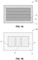
- the metal PCB heat spreader 150 may comprise a metal base 151.
- the metal base 151 may include copper, aluminum, or any other metal.
- the metal base 151 may have a thickness that is up to approximately 5.0mm. In a particular embodiment, the thickness of the metal base 151 may be between approximately 0.3mm and approximately 3.0mm. As used herein, “approximately” may refer to a value that is within ten percent of the stated value. For example, approximately 5.0mm may refer to a range between 4.5mm and 5.5mm.
- the metal base 151 may have a bare surface, as shown.
- a dielectric layer (not shown) may be provide over the metal base 151. The dielectric layer may be a thin layer (e.g., 1 ⁇ m or thinner).
- traces 153 and 152 may be provided over the metal base 151.
- the traces 153 and 152 may be copper traces, or the like.
- the traces 153 and 152 may be fabricated with traditional plating processes for semiconductor packaging applications, as will be described in greater detail below.
- the traces 153 and 152 may be formed directly on the metal base 151.
- one or both of the traces 153 and 152 may be separated from the metal base 151 by a dielectric layer, as described above.
- the traces 153 and 152 may be used to provide top side connections to features on the underlying package substrate.
- one or more dies may be coupled to VRs by the traces 153 and 152.
- the traces 153 and 152 are a plurality of parallel lines.
- the traces 153 and 152 may have any shape in order to provide the necessary routing between components on the package substrate.
- the electronic package 140 may comprise a package substrate 141.
- the package substrate 141 may include conductive routing and other electrical features (not shown).
- the package substrate 141 may comprise a plurality of laminated dielectric layers with the conductive routing between the dielectric layers.
- the package substrate 141 may include a core, though coreless embodiments may also be used.
- a pair of dies 142 are illustrated on the package substrate 141.
- the dies 142 may be single dies. In other embodiments, the dies 142 may be the top dies of a stack of dies. That is, additional dies may be provided below the pair of dies 142 in some embodiments.
- a VR block 143 may also be provided on the package substrate 141. The VR block 143 may be provided between the pair of dies 142. As such, the traces 153 and 152 described above can be used to connect the top of the dies 142 to the VR block 143.
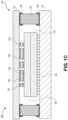
- the electronic system 100 may include a package substrate 141.
- the package substrate 141 in Figure 1C may be substantially similar to the package substrate 141 described above with respect to Figure 1B .
- a stack of dies 142 and 143 are coupled to the package substrate 141 by solder balls 144 or other interconnect architectures.
- two dies 142 and 143 are provided in the stack of dies.
- one or more dies may be included in the stack.
- the metal PCB heat spreader 150 may be connected to the top surface of the die 142.
- the metal PCB heat spreader 150 may include a metal base 151 and traces 152 and 153.
- the metal base 151 and the traces 152 and 153 may be substantially similar to the metal base 151 and traces 152 and 153 described in greater detail above.
- the traces 152 and 153 may be coupled to pads 146 and 147 by solder 145 or the like.
- the edges of the metal base 151 may be supported by a stiffener 155.
- the stiffener 155 may be coupled between the metal base 151 and the package substrate 141.
- Sealant 156 or other adhesives may be used to secure the stiffener 155 to the metal base 151 and the package substrate 141.
- the stiffener 155 is a stiff material (e.g., aluminum, etc.) that provides mechanical stiffness to the underlying package substrate 141 in order to reduce warpage or other deformation of the package substrate 141.
- the metal PCB heat spreader 250 may include a metal base 251.
- the metal base 251 may be copper, aluminum, or any other suitable metal material.
- the thickness of the metal base 251 may be between approximately 5.0mm or smaller. Larger thicknesses provide more thermal mass to improve spreading of heat.
- a dielectric layer 257 may be provided over a bottom surface of the metal base 251.
- the dielectric layer 257 may be any suitable dielectric material.
- the dielectric layer 257 may comprise silicon and nitrogen (e.g., silicon nitride).
- a thickness of the dielectric layer 257 may be approximately 1 ⁇ m or less. Small thicknesses allow for improved removal of thermal energy from the underlying dies.
- the metal PCB heat spreader 250 may include first traces 252 and second traces 253.
- the first traces 252 may be provided over the dielectric layer 257. That is, the first traces 252 may be electrically isolated from the metal base 251.
- the second traces 253 may pass through the dielectric layer 257. As such, the second traces 253 may be electrically coupled to the metal base 251.
- Such traces 253 may be suitable for grounded traces when the metal base 251 is held at ground potential.
- the width of the first traces 252 is greater than the width of the second traces 253.
- the widths of the first traces 252 and the second traces 253 may be any suitable width, and they do not have to have the same configuration shown in Figure 2 .
- FIG. 3A-3E a series of cross-sectional illustrations depicting electronic systems 300 that include various metal PCB heat spreader architectures is shown, in accordance with an embodiment. That is, the structure of the metal PCB heat spreader is flexible in order to accommodate various system architectures.
- the electronic system 300 may comprise a package substrate 341.
- One or more dies 342 and 343 may be coupled to the package substrate 341 by solder balls 344 or other interconnect architectures.
- a metal PCB heat spreader 350 is coupled to the top die 342.
- the metal PCB heat spreader 350 may include a metal base 351.
- One or more first traces 352 and second traces 353 may be provided over the metal base 351.
- first traces 352 and the second traces 353 may be directly contacting the metal base 351, or one or both of the first traces 352 and the second traces 353 may be separated from the metal base 351 by a thin dielectric layer (not shown).
- the metal PCB heat spreader 350 may be coupled to the top die 342 by solder 345 or the like.
- first pads 346 and second pads 347 on the top surface of the top die 342 may be connected to the first traces 352 and the second traces 353 by the solder 345.
- the first traces 352 and the second traces 353 electrically couple the first pads 346 and the second pads 347 to pads on a different structure out of the plane of Figure 3A .
- the die 342 may be coupled to a VR block that is also provided on the package substrate (e.g., behind or in front of the dies 342 and 343).
- the outer edge of the metal base 351 may also be coupled to the package substrate 341.
- a sealant 358 or the like may mechanically couple the metal base 351 to the package substrate 341. That is, in some embodiments, there might not be a stiffener between the metal base 351 and the package substrate 341, as is the case in the embodiment described above with respect to Figure 1C .
- the electronic system 300 may comprise a package substrate 341.
- One or more dies 342 and 343 may be coupled to the package substrate 341 by solder balls 344 or other interconnect architectures.
- a metal PCB heat spreader 350 is coupled to the top die 342.
- the metal PCB heat spreader 350 may include a metal base 351.
- One or more first traces 352 and second traces 353 may be provided over the metal base 351.
- first traces 352 and the second traces 353 may be directly contacting the metal base 351, or one or both of the first traces 352 and the second traces 353 may be separated from the metal base 351 by a thin dielectric layer (not shown).
- the metal PCB heat spreader 350 may be coupled to the top die 342 by solder 345 or the like.
- first pads 346 and second pads 347 on the top surface of the top die 342 may be connected to the first traces 352 and the second traces 353 by the solder 345.
- the first traces 352 and the second traces 353 electrically couple the first pads 346 and the second pads 347 to pads on a different structure out of the plane of Figure 3B .
- the die 342 may be coupled to a VR block that is also provided on the package substrate (e.g., behind or in front of the dies 342 and 343).
- the metal base 351 may be coupled to the package substrate 341 by a mold layer 360.
- the mold layer 360 may be an epoxy or any other molding compound.
- the mold layer 360 may also surround the solder 345 that connects the traces 352 and 353 to the pads 346 and 347.
- the electronic system 300 may comprise a package substrate 341.
- One or more dies 342 and 343 may be coupled to the package substrate 341 by solder balls 344 or other interconnect architectures.
- a metal PCB heat spreader 350 is coupled to the top die 342.
- the metal PCB heat spreader 350 may include a metal base 351.
- One or more first traces 352 and second traces 353 may be provided over the metal base 351.
- first traces 352 and the second traces 353 may be directly contacting the metal base 351, or one or both of the first traces 352 and the second traces 353 may be separated from the metal base 351 by a thin dielectric layer (not shown).
- the metal PCB heat spreader 350 may be coupled to the top die 342 by solder 345 or the like.
- first pads 346 and second pads 347 on the top surface of the top die 342 may be connected to the first traces 352 and the second traces 353 by the solder 345.
- the first traces 352 and the second traces 353 electrically couple the first pads 346 and the second pads 347 to pads on a different structure out of the plane of Figure 3C .
- the die 342 may be coupled to a VR block that is also provided on the package substrate (e.g., behind or in front of the dies 342 and 343).
- the outer edge of the metal base 351 may include legs 361.
- the legs 361 extend down from the metal base 351 towards the package substrate 341.
- the legs 361 are angled. Though, in other embodiments, the legs 361 may be substantially vertical.
- footings 362 may be provided at the bottom of the legs 361. The footings 362 may be used to connect the metal PCB heat spreader 350 to the package substrate 341. For example, a sealant 358 or other adhesive may be used to mechanically couple the footings 362 to the package substrate 341.
- the electronic system 300 may comprise a package substrate 341.
- One or more dies 342 and 343 may be coupled to the package substrate 341 by solder balls 344 or other interconnect architectures.
- a metal PCB heat spreader 350 is coupled to the top die 342.
- the metal PCB heat spreader 350 may include a metal base 351.
- One or more first traces 352 and second traces 353 may be provided over the metal base 351.
- first traces 352 and the second traces 353 may be directly contacting the metal base 351, or one or both of the first traces 352 and the second traces 353 may be separated from the metal base 351 by a thin dielectric layer (not shown).
- the metal PCB heat spreader 350 may be coupled to the top die 342 by solder 345 or the like.
- first pads 346 and second pads 347 on the top surface of the top die 342 may be connected to the first traces 352 and the second traces 353 by the solder 345.
- the first traces 352 and the second traces 353 electrically couple the first pads 346 and the second pads 347 to pads on a different structure out of the plane of Figure 3D .
- the die 342 may be coupled to a VR block that is also provided on the package substrate (e.g., behind or in front of the dies 342 and 343).
- the outer edge of the metal base 351 may end so that the edge of the dies 342 and 343 are substantially coplanar with edges of the metal base 351. That is, the footprint of the metal base 351 may be substantially similar to the footprint of the dies 342 and 343. Though, it is to be appreciated that the footprint of the metal base 351 may be larger or smaller than a footprint of the dies 342 and 343. In such an embodiment, the metal base 351 may not be directly coupled to the package substrate 341.
- a stiffener 355 may be provided around the dies 342 and 343. The stiffener 355 may be coupled to the package substrate by a sealant 358 or other adhesive.
- the stiffener 355 is a rigid structure (e.g., aluminum, stainless steel, or other metal) that provides mechanical rigidity to the underlying package substrate 341 in order to minimize warpage or other mechanical deformation.
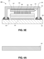
- the electronic system 300 may comprise a package substrate 341.
- One or more dies 342 and 343 may be coupled to the package substrate 341 by solder balls 344 or other interconnect architectures.
- a metal PCB heat spreader 350 is coupled to the top die 342.
- the metal PCB heat spreader 350 may include a metal base 351.
- One or more first traces 352 and second traces 353 may be provided over the metal base 351.
- first traces 352 and the second traces 353 may be directly contacting the metal base 351, or one or both of the first traces 352 and the second traces 353 may be separated from the metal base 351 by a thin dielectric layer (not shown).
- the metal PCB heat spreader 350 may be coupled to the top die 342 by solder 345 or the like.
- first pads 346 and second pads 347 on the top surface of the top die 342 may be connected to the first traces 352 and the second traces 353 by the solder 345.
- the first traces 352 and the second traces 353 electrically couple the first pads 346 and the second pads 347 to pads on a different structure out of the plane of Figure 3E .
- the die 342 may be coupled to a VR block that is also provided on the package substrate (e.g., behind or in front of the dies 342 and 343).
- an IHS 370 may be provided over the metal base 351.
- the IHS 370 may be thermally coupled to the metal base 351 by a TIM 371.
- the IHS 370 extends laterally past the edges of the metal baser 351. Legs may extend down from the top of the IHS 370 in order to couple with the package substrate 341.
- a sealant 358 or other adhesive may be used to mechanically couple the IHS 370 to the package substrate 341.
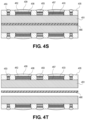
- FIG. 4A-4T a series of cross-sectional illustrations depicting a process for forming a metal PCB heat spreader is shown, in accordance with an embodiment.
- the metal base 451 may include copper, aluminum, or any other suitable metal material.
- the metal base 451 may have a thickness that is approximately 5.0mm or less. In a particular embodiment, the thickness of the metal base 451 is between approximately 0.3mm and approximately 3.0mm.
- FIG. 4B a cross-sectional illustration of a pair of metal bases 451 A and 451 B are shown.
- the metal bases 451 A and 451 B may be temporarily adhered to each other by a temporary adhesive 480.
- Such an architecture allows for the fabrication of two metal PCB heat spreaders substantially in parallel. That is, operations to the top metal base 451 A may also be implemented on the bottom metal base 451 B . For simplicity and ease of illustration, only the top metal base 451 A is shown until the end, where both sides are again illustrated.
- the dielectric layer 457 may be a thin layer.
- the dielectric layer 457 may have a thickness of approximately 1 ⁇ m or smaller.
- the dielectric layer 457 may comprise silicon and nitrogen (e.g., silicon nitride) or any other suitable dielectric material.
- the adhesion layer 431 may include HMDS or the like. Such an adhesion layer improves the adhesion of a subsequently added liquid photoresist material.
- FIG. 4E a cross-sectional illustration of the metal base 451 after a photoresist layer 432 is disposed over the adhesion layer 431.
- the photoresist layer 432 may be disposed with a spin coating process or any other suitable deposition process.
- the patterning process may include an exposure of the photoresist and a developing process. As such, a soft mask structure is provided for subsequent patterning of the dielectric layer 457.
- the patterning process may be an etching process, such as with a wet etching chemistry.
- the patterning of the dielectric layer 457 re-exposes portions of the metal base 451.
- FIG. 4H a cross-sectional illustration of the metal base 451 after the patterning layers are removed is shown, in accordance with an embodiment.
- the patterning layers may be removed with a stripping process or the like.
- the seed layer 433 may be a titanium or copper seed layer.
- the seed layer 433 may be formed with a deposition process, such as a chemical or physical vapor deposition process.
- An electroless process may also be used to form the seed layer 433.
- FIG. 4J a cross-sectional illustration of the metal base 451 after a dry film resist (DFR) 434 is disposed over the top surfaces and patterned is shown, in accordance with an embodiment.
- the DFR 434 may be patterned to form openings over the dielectric layer 457 and over regions without the dielectric layer 457.
- FIG. 4K a cross-sectional illustration of the metal base 451 after traces 452 and 453 are formed is shown, in accordance with an embodiment.
- the traces 452 are over the dielectric layer 457, and the traces 453 are provided over the metal base 451 without the dielectric layer 457 between them.
- the traces 452 and the traces 453 may be formed with an electrolytic plating process or the like.
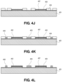
- FIG. 4L a cross-sectional illustration of the metal base 451 after the DFR 434 is removed is shown, in accordance with an embodiment.
- the DFR 434 may be removed with a stripping process or the like.
- FIG. 4M a cross-sectional illustration of the metal base 451 after the seed layer 433 is stripped is shown, in accordance with an embodiment.
- the exposed portions of the seed layer 433 may be removed with an etching process or the like. It is to be appreciated that portions of the seed layer 433 may persist below the traces 452 and 453 in some embodiments.
- the thermally conductive polymer 435 may include filler particles that improve the thermal conductivity, without being conductive in order to prevent the traces 452 and 452 from shorting together.
- the filler particles may comprise BN, AlN, Al 2 O 3 , or the like.
- FIG. 4O a cross-sectional illustration of the metal base 451 after openings 437 and 436 are provided into the thermally conductive polymer 435 is shown, in accordance with an embodiment.
- the openings 437 and 436 may be formed with a laser drilling process. Sidewalls of the openings 437 and 436 may be tapered, as shown in Figure 4O .
- the surface finishes 438 may comprise nickel or any other suitable surface finish material.
- solder 439 may be disposed with a paste printing operation or any other suitable solder deposition process.
- solder 439 may be an InAg solder paste.
- FIG. 4R a cross-sectional illustration of the metal base 451 after the solder 439 is reflown is shown, in accordance with an embodiment.
- the reflowing process may result in the formation of solder bumps, which can be used to couple the metal base 451 to pads on underlying dies as described in greater detail above.
- top side structure and the bottom side structure may be substantially similar to each other.
- the adhesive 480 may be deactivated (e.g., with heat or the like).
- the topside and the bottom side structures may be peeled off of the adhesive.
- the top and bottom structures may be singulated into individual units. Only a single unit is shown in Figures 4A-4T , but it is to be appreciated that multiple iterations of the metal PCB heat spreader may be formed on each of the topside and the bottom side.
- the electronic system 590 may include a package substrate 541.
- a stack of dies 542 and 543 are coupled to the package substrate 541 by solder balls 544 or other interconnect architectures.
- two dies 542 and 543 are provided in the stack of dies.
- one or more dies may be included in the stack.
- the metal PCB heat spreader 550 may be connected to the top surface of the die 542.
- the metal PCB heat spreader 550 may include a metal base 551 and traces 552 and 553.
- the traces 552 and 553 may be coupled to pads 546 and 547 by solder 545 or the like.
- the edges of the metal base 551 may be supported by a stiffener 555.
- the stiffener 555 may be coupled between the metal base 551 and the package substrate 541.
- Sealant 556 or other adhesives may be used to secure the stiffener 555 to the metal base 551 and the package substrate 541.
- the sealant 566 may comprise silicone, urethane, epoxy, or the like.
- the stiffener 555 is a stiff material (e.g., aluminum, etc.) that provides mechanical stiffness to the underlying package substrate 541 in order to reduce warpage or other deformation of the package substrate 541.
- the package substrate 541 may be coupled to a board 591, such as a PCB.
- the package substrate 541 is coupled to the board 591 by interconnects 592. While shown as solder balls, it is to be appreciated that the interconnects 592 may be any suitable interconnect architecture, such as sockets or the like.
- the package substrate 541 and metal PCB heat spreader 550 are substantially similar to the embodiments shown above in Figure 1C .
- the electronic system 590 may include any of the metal PCB heat spreaders described in greater detail herein.
- FIG. 6 illustrates a computing device 600 in accordance with one implementation of the invention.
- the computing device 600 houses a board 602.
- the board 602 may include a number of components, including but not limited to a processor 604 and at least one communication chip 606.
- the processor 604 is physically and electrically coupled to the board 602.
- the at least one communication chip 606 is also physically and electrically coupled to the board 602.
- the communication chip 606 is part of the processor 604.
- volatile memory e.g., DRAM
- non-volatile memory e.g., ROM
- flash memory e.g., a graphics processor, a digital signal processor, a crypto processor, a chipset, an antenna, a display, a touchscreen display, a touchscreen controller, a battery, an audio codec, a video codec, a power amplifier, a global positioning system (GPS) device, a compass, an accelerometer, a gyroscope, a speaker, a camera, and a mass storage device (such as hard disk drive, compact disk (CD), digital versatile disk (DVD), and so forth).
- volatile memory e.g., DRAM
- non-volatile memory e.g., ROM
- flash memory e.g., a graphics processor, a digital signal processor, a crypto processor, a chipset, an antenna, a display, a touchscreen display, a touchscreen controller, a battery, an audio codec, a video codec,
- the communication chip 606 enables wireless communications for the transfer of data to and from the computing device 600.
- wireless and its derivatives may be used to describe circuits, devices, systems, methods, techniques, communications channels, etc., that may communicate data through the use of modulated electromagnetic radiation through a non-solid medium. The term does not imply that the associated devices do not contain any wires, although in some embodiments they might not.
- the communication chip 606 may implement any of a number of wireless standards or protocols, including but not limited to Wi-Fi (IEEE 802.11 family), WiMAX (IEEE 802.16 family), IEEE 802.20, long term evolution (LTE), Ev-DO, HSPA+, HSDPA+, HSUPA+, EDGE, GSM, GPRS, CDMA, TDMA, DECT, Bluetooth, derivatives thereof, as well as any other wireless protocols that are designated as 3G, 4G, 5G, and beyond.
- the computing device 600 may include a plurality of communication chips 606.
- a first communication chip 606 may be dedicated to shorter range wireless communications such as Wi-Fi and Bluetooth and a second communication chip 606 may be dedicated to longer range wireless communications such as GPS, EDGE, GPRS, CDMA, WiMAX, LTE, Ev-DO, and others.
- the processor 604 of the computing device 600 includes an integrated circuit die packaged within the processor 604.
- the integrated circuit die of the processor may part of an electronic package that includes a metal PCB heat spreader that provides top electrical connections, in accordance with embodiments described herein.
- the term "processor" may refer to any device or portion of a device that processes electronic data from registers and/or memory to transform that electronic data into other electronic data that may be stored in registers and/or memory.
- the communication chip 606 also includes an integrated circuit die packaged within the communication chip 606.
- the integrated circuit die of the communication chip may part of an electronic package that includes a metal PCB heat spreader that provides top electrical connections, in accordance with embodiments described herein.
- Example 1 an electronic package, comprising: a package substrate; a die on the package substrate; a voltage regulator on the package substrate adjacent to the die; and a metal printed circuit board (PCB) heat spreader, wherein a trace on the metal PCB heat spreader couples the die to the voltage regulator.
- PCB metal printed circuit board
- Example 2 the electronic package of Example 1, wherein the metal PCB heat spreader comprises a metal core, and wherein a dielectric layer is between the metal core and the trace.
- Example 3 the electronic package of Example 2, wherein a thickness of the metal core is approximately 5.0mm or less.
- Example 4 the electronic package of Example 2 or Example 3, wherein the metal core is grounded.
- Example 5 the electronic package of Examples 2-4, wherein the metal core comprises copper.
- Example 6 the electronic package of Examples 1-5, wherein a footprint of the metal PCB heat spreader is larger than a combined footprint of the die and the voltage regulator.
- Example 7 the electronic package of Examples 1-6, wherein the metal PCB heat spreader is coupled to the package substrate by a stiffener.
- Example 8 the electronic package of Examples 1-7, wherein the metal PCB heat spreader is coupled to the package substrate by a sealant.
- Example 9 the electronic package of Examples 1-8, wherein metal PCB heat spreader comprises legs that are coupled to the package substrate by a sealant.
- Example 10 the electronic package of Examples 1-9, further comprising a stiffener surrounding the die.
- Example 11 the electronic package of Examples 1-10, further comprising an integrated heat spreader over the PCB heat spreader.
- Example 12 the electronic package of Examples 1-11, further comprising a second die between the die and the package substrate.
- Example 13 a metal PCB heat spreader, comprising: a metal layer; a dielectric layer over the metal layer; a first trace on a surface of the dielectric layer; and a second trace that pass through the dielectric layer and is coupled to the metal layer.
- Example 14 the metal PCB heat spreader of Example 13, wherein the metal layer comprises copper.
- Example 15 the metal PCB heat spreader of Example 13 or Example 14, wherein the metal layer has a thickness of approximately 5.0mm or less.
- Example 16 the metal PCB heat spreader of Examples 13-15, further comprising legs that extend down from the metal layer, wherein the legs are coupled to the metal layer.
- Example 17 the metal PCB heat spreader of Examples 13-16, wherein the first trace is electrically isolated from the metal layer.
- Example 18 a method of forming a metal PCB heat spreader, comprising: providing a metal layer; forming a dielectric layer over the metal layer; patterning the dielectric layer; forming a seed layer over the dielectric layer; forming a patterning layer over the seed layer, wherein first openings are provided over the dielectric layer and second openings are provided over the metal layer; plating the first openings and the second openings to form first traces in the first openings and second traces in the second openings; removing the seed layer; disposing a thermally conductive polymer over the first traces and the second traces; forming openings into the thermally conductive polymer over the first traces and the second traces; and disposing a solder in the openings into the thermally conductive polymer.
- Example 19 the method of Example 18, further comprising: a second metal layer attached to the first metal layer by a temporary adhesive, and wherein a second metal PCB heat spreader is formed on the second metal layer.
- Example 20 the method of Example 19, further comprising: releasing the temporary adhesive after the metal PCB heat spreader and the second metal PCB heat spreader are formed.
- Example 21 the method of Examples 18-20, wherein the first openings are wider than the second openings.
- Example 22 the method of Examples 18-21, further comprising: forming a surface finish over the first traces and the second traces before the solder is disposed into the openings.
- Example 23 an electronic system, comprising: a board; a package substrate coupled to the board; a first die on the package substrate; a second die on the package substrate; a voltage regulator on the package substrate between the first die and the second die; and a metal printed circuit board (PCB) heat spreader, wherein a first trace on the metal PCB heat spreader couples the first die to the voltage regulator and a second trace on the metal PCB heat spreader couples the second die to the voltage regulator.
- PCB metal printed circuit board
- Example 24 the electronic system of Example 23, wherein the metal PCB heat spreader comprises a metal core, and wherein a dielectric layer is between the metal core and the first trace and the second trace.
- Example 25 the electronic package of Example 24, wherein a thickness of the metal core is approximately 5.0mm or less.
Landscapes
- Cooling Or The Like Of Semiconductors Or Solid State Devices (AREA)
- Chemical & Material Sciences (AREA)
- Engineering & Computer Science (AREA)
- Materials Engineering (AREA)
Applications Claiming Priority (1)
| Application Number | Priority Date | Filing Date | Title |
|---|---|---|---|
| US17/710,753 US20230317706A1 (en) | 2022-03-31 | 2022-03-31 | Metal pcb for topside power delivery |
Publications (1)
| Publication Number | Publication Date |
|---|---|
| EP4254484A1 true EP4254484A1 (de) | 2023-10-04 |
Family
ID=85239096
Family Applications (1)
| Application Number | Title | Priority Date | Filing Date |
|---|---|---|---|
| EP23156628.2A Pending EP4254484A1 (de) | 2022-03-31 | 2023-02-14 | Metall-pcb zur oberseitigen stromversorgung |
Country Status (2)
| Country | Link |
|---|---|
| US (1) | US20230317706A1 (de) |
| EP (1) | EP4254484A1 (de) |
Families Citing this family (1)
| Publication number | Priority date | Publication date | Assignee | Title |
|---|---|---|---|---|
| WO2025264667A1 (en) * | 2024-06-17 | 2025-12-26 | The Trustees Of Princeton University | Ai enabled synthesis of electromagnetic structures and high frequency circuits |
Citations (4)
| Publication number | Priority date | Publication date | Assignee | Title |
|---|---|---|---|---|
| US20090289354A1 (en) * | 2008-05-20 | 2009-11-26 | Infineon Technologies Ag | Electronic module |
| US20210398895A1 (en) * | 2020-06-22 | 2021-12-23 | Intel Corporation | Power delivery structures |
| EP4156263A2 (de) * | 2021-09-24 | 2023-03-29 | INTEL Corporation | Rückseitige stromversorgung für elektronische vorrichtungen |
| WO2023115450A1 (en) * | 2021-12-23 | 2023-06-29 | Intel Corporation | Integrated top side power delivery thermal technology |
Family Cites Families (6)
| Publication number | Priority date | Publication date | Assignee | Title |
|---|---|---|---|---|
| US7173329B2 (en) * | 2001-09-28 | 2007-02-06 | Intel Corporation | Package stiffener |
| US7739876B2 (en) * | 2006-12-27 | 2010-06-22 | Intel Corporation | Socket enabled current delivery to a thermoelectric cooler to cool an in-substrate voltage regulator |
| US20110272179A1 (en) * | 2010-05-06 | 2011-11-10 | Vasoya Kalu K | Printed Circuit Board with Embossed Hollow Heatsink Pad |
| ES2699495T3 (es) * | 2011-02-08 | 2019-02-11 | Cambridge Nanotherm Ltd | Sustrato de metal aislado |
| US10529677B2 (en) * | 2018-04-27 | 2020-01-07 | Advanced Micro Devices, Inc. | Method and apparatus for power delivery to a die stack via a heat spreader |
| US11004768B2 (en) * | 2019-08-01 | 2021-05-11 | Intel Corporation | Multi-chip package with partial integrated heat spreader |
-
2022
- 2022-03-31 US US17/710,753 patent/US20230317706A1/en active Pending
-
2023
- 2023-02-14 EP EP23156628.2A patent/EP4254484A1/de active Pending
Patent Citations (4)
| Publication number | Priority date | Publication date | Assignee | Title |
|---|---|---|---|---|
| US20090289354A1 (en) * | 2008-05-20 | 2009-11-26 | Infineon Technologies Ag | Electronic module |
| US20210398895A1 (en) * | 2020-06-22 | 2021-12-23 | Intel Corporation | Power delivery structures |
| EP4156263A2 (de) * | 2021-09-24 | 2023-03-29 | INTEL Corporation | Rückseitige stromversorgung für elektronische vorrichtungen |
| WO2023115450A1 (en) * | 2021-12-23 | 2023-06-29 | Intel Corporation | Integrated top side power delivery thermal technology |
Also Published As
| Publication number | Publication date |
|---|---|
| US20230317706A1 (en) | 2023-10-05 |
Similar Documents
| Publication | Publication Date | Title |
|---|---|---|
| US11824018B2 (en) | Heterogeneous nested interposer package for IC chips | |
| US12087695B2 (en) | Hybrid fan-out architecture with EMIB and glass core for heterogeneous die integration applications | |
| US12525562B2 (en) | Assembly of 2XD module using high density interconnect bridges | |
| CN106356340B (zh) | 半导体器件及其制造方法 | |
| US11769735B2 (en) | Chiplet first architecture for die tiling applications | |
| KR102952166B1 (ko) | 초박형 브리지 및 멀티-다이 초미세 피치 패치 아키텍처 및 제조 방법 | |
| US20200051899A1 (en) | Interposer package-on-package (pop) with solder array thermal contacts | |
| WO2019240898A1 (en) | Thermal management solutions for stacked integrated circuit devices | |
| US20230207522A1 (en) | Reconstituted wafer-to-wafer hybrid bonding interconnect architecture with known good dies | |
| US20230088392A1 (en) | Thermally conductive sleeves around tgvs for improved heat dissipation in glass core substrates or glass interposers | |
| US20230092740A1 (en) | Moat protection to prevent crack propagation in glass core substrates or glass interposers | |
| EP4254484A1 (de) | Metall-pcb zur oberseitigen stromversorgung | |
| US20240213156A1 (en) | Liquid metal wells for interconnect architectures | |
| CN117642854A (zh) | 玻璃贴片集成到电子装置封装中 | |
| US12616013B2 (en) | Dielectric bondable chiplet for package architecture including reset via simplification | |
| US20240203805A1 (en) | Embedded memory for glass core packages | |
| US20240071935A1 (en) | Glass die-to-die bridge and interposer for die first architecture |
Legal Events
| Date | Code | Title | Description |
|---|---|---|---|
| PUAI | Public reference made under article 153(3) epc to a published international application that has entered the european phase |
Free format text: ORIGINAL CODE: 0009012 |
|
| STAA | Information on the status of an ep patent application or granted ep patent |
Free format text: STATUS: THE APPLICATION HAS BEEN PUBLISHED |
|
| AK | Designated contracting states |
Kind code of ref document: A1 Designated state(s): AL AT BE BG CH CY CZ DE DK EE ES FI FR GB GR HR HU IE IS IT LI LT LU LV MC ME MK MT NL NO PL PT RO RS SE SI SK SM TR |
|
| STAA | Information on the status of an ep patent application or granted ep patent |
Free format text: STATUS: REQUEST FOR EXAMINATION WAS MADE |
|
| 17P | Request for examination filed |
Effective date: 20240404 |
|
| RBV | Designated contracting states (corrected) |
Designated state(s): AL AT BE BG CH CY CZ DE DK EE ES FI FR GB GR HR HU IE IS IT LI LT LU LV MC ME MK MT NL NO PL PT RO RS SE SI SK SM TR |