EP4254043B1 - Optische abtastvorrichtung, ansteuerungsverfahren für eine optische abtastvorrichtung und bildzeichensystem - Google Patents
Optische abtastvorrichtung, ansteuerungsverfahren für eine optische abtastvorrichtung und bildzeichensystem Download PDFInfo
- Publication number
- EP4254043B1 EP4254043B1 EP23164161.4A EP23164161A EP4254043B1 EP 4254043 B1 EP4254043 B1 EP 4254043B1 EP 23164161 A EP23164161 A EP 23164161A EP 4254043 B1 EP4254043 B1 EP 4254043B1
- Authority
- EP
- European Patent Office
- Prior art keywords
- driving
- driving frequency
- set value
- signal
- axis
- Prior art date
- Legal status (The legal status is an assumption and is not a legal conclusion. Google has not performed a legal analysis and makes no representation as to the accuracy of the status listed.)
- Active
Links
Images


Classifications
-
- H—ELECTRICITY
- H04—ELECTRIC COMMUNICATION TECHNIQUE
- H04N—PICTORIAL COMMUNICATION, e.g. TELEVISION
- H04N9/00—Details of colour television systems
- H04N9/12—Picture reproducers
- H04N9/31—Projection devices for colour picture display, e.g. using electronic spatial light modulators [ESLM]
- H04N9/3129—Projection devices for colour picture display, e.g. using electronic spatial light modulators [ESLM] scanning a light beam on the display screen
- H04N9/3135—Driving therefor
-
- G—PHYSICS
- G02—OPTICS
- G02B—OPTICAL ELEMENTS, SYSTEMS OR APPARATUS
- G02B26/00—Optical devices or arrangements for the control of light using movable or deformable optical elements
- G02B26/08—Optical devices or arrangements for the control of light using movable or deformable optical elements for controlling the direction of light
- G02B26/0816—Optical devices or arrangements for the control of light using movable or deformable optical elements for controlling the direction of light by means of one or more reflecting elements
- G02B26/0833—Optical devices or arrangements for the control of light using movable or deformable optical elements for controlling the direction of light by means of one or more reflecting elements the reflecting element being a micromechanical device, e.g. a MEMS mirror, DMD
- G02B26/0858—Optical devices or arrangements for the control of light using movable or deformable optical elements for controlling the direction of light by means of one or more reflecting elements the reflecting element being a micromechanical device, e.g. a MEMS mirror, DMD the reflecting means being moved or deformed by piezoelectric means
-
- G—PHYSICS
- G02—OPTICS
- G02B—OPTICAL ELEMENTS, SYSTEMS OR APPARATUS
- G02B26/00—Optical devices or arrangements for the control of light using movable or deformable optical elements
- G02B26/08—Optical devices or arrangements for the control of light using movable or deformable optical elements for controlling the direction of light
- G02B26/10—Scanning systems
- G02B26/101—Scanning systems with both horizontal and vertical deflecting means, e.g. raster or XY scanners
-
- G—PHYSICS
- G02—OPTICS
- G02B—OPTICAL ELEMENTS, SYSTEMS OR APPARATUS
- G02B26/00—Optical devices or arrangements for the control of light using movable or deformable optical elements
- G02B26/08—Optical devices or arrangements for the control of light using movable or deformable optical elements for controlling the direction of light
- G02B26/10—Scanning systems
- G02B26/105—Scanning systems with one or more pivoting mirrors or galvano-mirrors
-
- G—PHYSICS
- G03—PHOTOGRAPHY; CINEMATOGRAPHY; ANALOGOUS TECHNIQUES USING WAVES OTHER THAN OPTICAL WAVES; ELECTROGRAPHY; HOLOGRAPHY
- G03B—APPARATUS OR ARRANGEMENTS FOR TAKING PHOTOGRAPHS OR FOR PROJECTING OR VIEWING THEM; APPARATUS OR ARRANGEMENTS EMPLOYING ANALOGOUS TECHNIQUES USING WAVES OTHER THAN OPTICAL WAVES; ACCESSORIES THEREFOR
- G03B21/00—Projectors or projection-type viewers; Accessories therefor
- G03B21/005—Projectors using an electronic spatial light modulator but not peculiar thereto
- G03B21/008—Projectors using an electronic spatial light modulator but not peculiar thereto using micromirror devices
-
- G—PHYSICS
- G03—PHOTOGRAPHY; CINEMATOGRAPHY; ANALOGOUS TECHNIQUES USING WAVES OTHER THAN OPTICAL WAVES; ELECTROGRAPHY; HOLOGRAPHY
- G03B—APPARATUS OR ARRANGEMENTS FOR TAKING PHOTOGRAPHS OR FOR PROJECTING OR VIEWING THEM; APPARATUS OR ARRANGEMENTS EMPLOYING ANALOGOUS TECHNIQUES USING WAVES OTHER THAN OPTICAL WAVES; ACCESSORIES THEREFOR
- G03B21/00—Projectors or projection-type viewers; Accessories therefor
- G03B21/14—Details
- G03B21/20—Lamp housings
- G03B21/2006—Lamp housings characterised by the light source
- G03B21/2033—LED or laser light sources
-
- G—PHYSICS
- G03—PHOTOGRAPHY; CINEMATOGRAPHY; ANALOGOUS TECHNIQUES USING WAVES OTHER THAN OPTICAL WAVES; ELECTROGRAPHY; HOLOGRAPHY
- G03B—APPARATUS OR ARRANGEMENTS FOR TAKING PHOTOGRAPHS OR FOR PROJECTING OR VIEWING THEM; APPARATUS OR ARRANGEMENTS EMPLOYING ANALOGOUS TECHNIQUES USING WAVES OTHER THAN OPTICAL WAVES; ACCESSORIES THEREFOR
- G03B21/00—Projectors or projection-type viewers; Accessories therefor
- G03B21/14—Details
- G03B21/20—Lamp housings
- G03B21/2066—Reflectors in illumination beam
-
- G—PHYSICS
- G09—EDUCATION; CRYPTOGRAPHY; DISPLAY; ADVERTISING; SEALS
- G09G—ARRANGEMENTS OR CIRCUITS FOR CONTROL OF INDICATING DEVICES USING STATIC MEANS TO PRESENT VARIABLE INFORMATION
- G09G3/00—Control arrangements or circuits, of interest only in connection with visual indicators other than cathode-ray tubes
- G09G3/02—Control arrangements or circuits, of interest only in connection with visual indicators other than cathode-ray tubes by tracing or scanning a light beam on a screen
- G09G3/025—Control arrangements or circuits, of interest only in connection with visual indicators other than cathode-ray tubes by tracing or scanning a light beam on a screen with scanning or deflecting the beams in two directions or dimensions
-
- H—ELECTRICITY
- H04—ELECTRIC COMMUNICATION TECHNIQUE
- H04N—PICTORIAL COMMUNICATION, e.g. TELEVISION
- H04N9/00—Details of colour television systems
- H04N9/12—Picture reproducers
- H04N9/31—Projection devices for colour picture display, e.g. using electronic spatial light modulators [ESLM]
- H04N9/3141—Constructional details thereof
- H04N9/3144—Cooling systems
-
- H—ELECTRICITY
- H04—ELECTRIC COMMUNICATION TECHNIQUE
- H04N—PICTORIAL COMMUNICATION, e.g. TELEVISION
- H04N9/00—Details of colour television systems
- H04N9/12—Picture reproducers
- H04N9/31—Projection devices for colour picture display, e.g. using electronic spatial light modulators [ESLM]
- H04N9/3191—Testing thereof
- H04N9/3194—Testing thereof including sensor feedback
Definitions
- the present disclosure relates to an optical scanning device, a driving method of an optical scanning device, and an image drawing system.
- a micromirror device (also referred to as a microscanner) has been known as one of micro electro mechanical systems (MEMS) devices manufactured using the silicon (Si) nanofabrication technique.
- MEMS micro electro mechanical systems
- An optical scanning device comprising the micromirror device has a small size and low power consumption and thus, is expected to be applied to image drawing systems such as laser displays or laser projectors.
- a mirror portion is formed to be capable of swinging around a first axis and a second axis that are orthogonal to each other, and the swing of the mirror portion around each axis causes light reflected by the mirror portion to be two-dimensionally scanned.
- a micromirror device that can perform Lissajous scanning of light by causing a mirror portion to resonate around each axis has been known.
- JP2016-184018A discloses a technique for selecting a driving frequency of a MEMS mirror and a frame rate that is a rate at which one cycle of scanning of the MEMS mirror is performed, based on an amplitude and a phase of the MEMS mirror.
- JP2018-132666A discloses an optical scanner and distance image sensor.
- JP2012-068349A discloses an optical scanner and optical ranging device using the same.
- US2008/231683A1 discloses an image forming apparatus and control method.
- the present disclosure is conceived in view of the above matter, and an object thereof is to provide an optical scanning device, a driving method of an optical scanning device, and an image drawing system that can constantly maintain a frequency ratio between a frequency of a first driving signal and a frequency of a second driving signal in a case of changing the frequency of the first driving signal and the frequency of the second driving signal.
- An optical scanning device is an optical scanning device comprising a mirror portion that has a reflecting surface on which an incidence ray is reflected, a first actuator that causes the mirror portion to swing around a first axis which is in a plane including the reflecting surface at a time of a standstill of the mirror portion, a second actuator that causes the mirror portion to swing around a second axis which is in the plane including the reflecting surface at the time of the standstill of the mirror portion and which intersects with the first axis, and at least one processor, in which the processor is configured to provide a first driving signal having a first driving frequency corresponding to a first set value to the first actuator, provide a second driving signal having a second driving frequency corresponding to a second set value to the second actuator, in a case of changing the first driving frequency and the second driving frequency, derive a greatest common divisor of the first set value and the second set value, change the first driving frequency by changing the first set value in units of a first number obtained by dividing the first set value by
- the processor may be configured to change the first driving frequency and the second driving frequency at the same timing based on a common clock signal.
- the common clock signal may be a clock signal in which a clock rises in accordance with a value obtained by multiplying the first set value by the second number, or a clock signal in which a clock rises in accordance with a value obtained by multiplying the second set value by the first number.
- the frequency ratio between the frequency of the first driving signal and the frequency of the second driving signal can be constantly maintained.
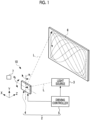
- the light source 3 is a laser device that emits, for example, laser light as the light beam L.
- the light source 3 outputs laser light of three colors of red (R), green (G), and blue (B).
- R red
- G green
- B blue
- the light source 3 perpendicularly irradiates a reflecting surface 20A (see Fig. 2 ) comprised in the mirror portion 20 with the light beam L in a state where the mirror portion 20 of the MMD 4 is at a standstill.
- the reflecting surface 20A is perpendicularly irradiated with the light beam L from the light source 3
- the light source 3 may be an obstacle in the drawing performed by scanning the surface to be scanned 6 with the light beam L.
- the reflecting surface 20A is perpendicularly irradiated with the light beam L emitted from the light source 3 by controlling the light beam L using an optical system such as a beam splitter.
- the optical system may include a lens or may not include a lens.
- an angle at which the reflecting surface 20A is irradiated with the light beam L emitted from the light source 3 is not limited to a perpendicular angle.
- the reflecting surface 20A may be irradiated with the light beam L in an inclined manner.
- the driving controller 5 outputs a driving signal to the light source 3 and to the MMD 4 based on optical scanning information.
- the light source 3 generates the light beam L based on the input driving signal and irradiates the MMD 4 with the light beam L.
- the MMD 4 causes the mirror portion 20 to swing around the first axis a 1 and around the second axis a 2 based on the input driving signal.
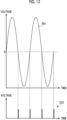
- the mirror portion 20 By causing the mirror portion 20 to resonate around each of the first axis a 1 and the second axis a 2 via the driving controller 5, the light beam L reflected by the mirror portion 20 is scanned onto the surface to be scanned 6 such that the light beam L draws a Lissajous waveform.
- This optical scanning method is called a Lissajous scanning method.
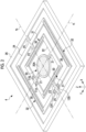
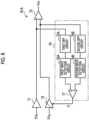
- the mirror portion 20 has the reflecting surface 20A for reflecting an incidence ray.
- the reflecting surface 20A is provided on one surface of the mirror portion 20 and is formed with a thin metal film of, for example, gold (Au), aluminum (Al), silver (Ag), or a silver alloy.
- a shape of the reflecting surface 20A is, for example, a circular shape centered at an intersection between the first axis a 1 and the second axis a 2 .
- the pair of second actuators 32 are arranged at positions that face each other with the second axis a 2 interposed therebetween.
- the second actuators 32 cause the mirror portion 20 to swing around the second axis a 2 by applying rotational torque about the second axis a 2 to the mirror portion 20 and to the first movable frame 22.
- the connecting portion 25 is arranged outside the second movable frame 24 at each of positions that face each other with the first axis a 1 interposed therebetween.
- the connecting portions 25 are connected to the second movable frame 24 on the second axis a 2 .
- the fixed frame 26 is a frame having a rectangular shape surrounding the second movable frame 24 and is connected to the second movable frame 24 through the connecting portion 25 on the second axis a 2 .
- a pair of second angle detection sensors 12A and 12B are provided in the second movable frame 24 near the second support portions 23 at positions that face each other with the second axis a 2 interposed therebetween.
- Each of the pair of second angle detection sensors 12A and 12B is configured with a piezoelectric element.
- Each of the second angle detection sensors 12A and 12B outputs a signal by converting a force applied by deformation of the second support portion 23 accompanied by rotational movement of the mirror portion 20 around the second axis a 2 into a voltage. That is, the second angle detection sensors 12A and 12B output signals corresponding to an angle of the mirror portion 20 around the second axis a 2 .
- wiring lines and electrode pads for providing driving signals to the first actuators 31 and the second actuators 32 are not shown.
- wiring lines and electrode pads for outputting signals from the first angle detection sensors 11A and 11B and from the second angle detection sensors 12A and 12B are not shown.
- a plurality of electrode pads are provided on the fixed frame 26.
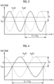
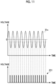
- a deflection angle (hereinafter, referred to as a "first deflection angle”) ⁇ 1 of the mirror portion 20 around the first axis a 1 is controlled based on the driving signal (hereinafter, referred to as a "first driving signal") provided to the first actuators 31 by the driving controller 5.
- the first driving signal is, for example, a sinusoidal alternating current voltage.
- the first driving signal includes a driving voltage waveform V 1A (t) applied to one of the pair of first actuators 31 and a driving voltage waveform V 1B (t) applied to the other.
- the driving voltage waveform V 1A (t) and the driving voltage waveform V 1B (t) are in anti-phase with each other (that is, have a phase difference of 180°).
- the first deflection angle ⁇ 1 is an angle at which a line normal to the reflecting surface 20A is inclined with respect to the Z direction in an XZ plane.
- a deflection angle (hereinafter, referred to as a "second deflection angle”) ⁇ 2 of the mirror portion 20 around the second axis a 2 is controlled based on the driving signal (hereinafter, referred to as a "second driving signal") provided to the second actuators 32 by the driving controller 5.
- the second driving signal is, for example, a sinusoidal alternating current voltage.
- the second driving signal includes a driving voltage waveform V 2A (t) applied to one of the pair of second actuators 32 and a driving voltage waveform V 2B (t) applied to the other.
- the driving voltage waveform V 2A (t) and the driving voltage waveform V 2B (t) are in anti-phase with each other (that is, have a phase difference of 180°).
- the second deflection angle ⁇ 2 is an angle at which the line normal to the reflecting surface 20A is inclined with respect to the Z direction in a YZ plane.
- V 1 is an amplitude voltage.
- V off1 is a bias voltage.
- V off1 may be zero.
- f d1 is a driving frequency (hereinafter, referred to as a "first driving frequency").
- t is time.
- the mirror portion 20 swings around the first axis a 1 with the first driving frequency f d1 .
- V 2A (t) and V 2B (t) are represented as follows.
- V 2 A t V off 2 + V 2 sin 2 ⁇ f d 2 t + ⁇
- V 2 B t V off 2 + V 2 sin 2 ⁇ f d 2 t + ⁇ + ⁇
- V 2 is an amplitude voltage.
- V off2 is a bias voltage.
- V off2 may be zero.
- f d2 is a driving frequency (hereinafter, referred to as a "second driving frequency").
- t is time.
- ⁇ is a phase difference between the driving voltage waveforms V 1A (t) and V 1B (t) and the driving voltage waveforms V 2A (t) and V 2B (t).
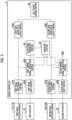
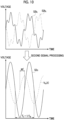
- the first signal processing portion 61A generates a signal (hereinafter, referred to as a "first angle detection signal”) S1c obtained by removing the vibration noise RN1 based on S1a 1 and S1a 2 output from the pair of first angle detection sensors 11A and 11B.
- the second signal processing portion 61B generates a signal (hereinafter, referred to as a "second angle detection signal”) S2c obtained by removing the vibration noise RN2 based on S2a 1 and S2a 2 output from the pair of second angle detection sensors 12A and 12B.
- the second signal processing portion 61B can be implemented by the same configuration as the first signal processing portion 61A and thus, will not be described.
- the second zero cross pulse output portion 63B generates the second zero cross pulse ZC2 at a timing at which the second angle detection signal S2c that is an alternating current signal crosses zero volts.
- the second zero cross pulse output portion 63B inputs the generated second zero cross pulse ZC2 into the light source driving portion 66.
- DDS direct digital synthesizer
- the second driving signal generation portion 60B can generate the second driving signal having the second driving frequency f d2 corresponding to the tuning word value M by setting the tuning word value M with which f out in Expression (1) results in the second driving frequency f d2 as a target.
- the derivation portion 64 acquires the temperature detected by the temperature sensor 7 and determines whether or not to change the first driving frequency f d1 and the second driving frequency f d2 based on the acquired temperature. Specifically, for example, the derivation portion 64 determines to change the first driving frequency f d1 and the second driving frequency f d2 in a case where an absolute value of a difference between a temperature in a case where the tuning word value M 1 and the tuning word value M 2 are most recently set and the acquired temperature is greater than or equal to a constant value (for example, 1°C).
- a constant value for example, 1°C
- M 1B is a value obtained by changing M 1A in units of the first number Q1.
- the derivation portion 64 derives the tuning word value M 2B in accordance with Expression (3) below.
- M 2 B M 2 A + n ⁇ Q 2
- M 2B is a value obtained by changing M 2A in units of the second number Q2.
- f d1B is obtained by substituting M 1B for M in Expression (1)
- f d2B is obtained by substituting M 2B for M in Expression (1).
- the clock signal generation portion 65 generates a common clock signal used for changing the first driving frequency f d1 via the first driving signal generation portion 60A and for changing the second driving frequency f d2 via the second driving signal generation portion 60B.
- the common clock signal is a clock signal in which a clock rises in accordance with a value obtained by multiplying M 1A by Q2.
- the common clock signal is a clock signal in which a clock rises each time a system clock rises (M 1A ⁇ Q2) times.
- One period of the common clock signal corresponds to Q2 periods of the first driving signal and to Q1 periods of the second driving signal.
- a period of time corresponding to one period of the common clock signal may be a period of time of one frame in drawing a motion image.
- the first driving signal generation portion 60A and the second driving signal generation portion 60B change the first driving frequency f d1 and the second driving frequency f d2 at the same timing based on the common clock signal generated by the clock signal generation portion 65.
- the first driving signal generation portion 60A changes the tuning word value M 1 of the DDS to M 1B derived by the derivation portion 64, at a timing when the clock of the common clock signal rises. Accordingly, the first driving signal generation portion 60A generates the first driving signal of which the first driving frequency f d1 is changed to f d1B , and provides the generated first driving signal to the pair of first actuators 31 through the first phase shift portion 62A.
- the second driving signal generation portion 60B changes the tuning word value M 2 of the DDS to M 2B derived by the derivation portion 64, at a timing when the same clock as the clock used by the first driving signal generation portion 60A rises. Accordingly, the second driving signal generation portion 60B generates the second driving signal of which the second driving frequency f d2 is changed to f d2B , and provides the generated second driving signal to the pair of second actuators 32 through the second phase shift portion 62B.
- the clock signal generated by the clock signal generation portion 65 may also be changed to a clock signal in which a clock rises each time the system clock rises (M 1B ⁇ Q2) times.
- Q2 is a quotient obtained by dividing M 2B by the greatest common divisor G of M 1B and M 2B .
- step S10 in Fig. 18 the derivation portion 64 acquires the temperature detected by the temperature sensor 7 and determines whether or not to change the first driving frequency f d1 and the second driving frequency f d2 based on the acquired temperature. In a case where this determination results in a negative determination, step S10 is executed again. In a case of a positive determination, the processing transitions to step S12.
- step S16 the derivation portion 64 determines the first driving frequency f d1 as a target based on the temperature and the temperature characteristic information acquired in step S10. In addition, the derivation portion 64 derives the tuning word value M 1 with which the first driving frequency f d1 as a target is obtained, in accordance with Expression (1) above. In addition, the derivation portion 64 determines n with which a value obtained by M 1A + n ⁇ Q1 is closest to the derived tuning word value M 1 . The derivation portion 64 derives the tuning word value M 1B in accordance with Expression (2) above. In addition, the derivation portion 64 derives the tuning word value M 2B in accordance with Expression (3) above.
- step S18 the first driving signal generation portion 60A and the second driving signal generation portion 60B wait until the common clock signal generated by the clock signal generation portion 65 rises. In a case where the common clock signal generated by the clock signal generation portion 65 rises, the determination in step S18 results in a positive determination, and the processing transitions to step S20.
- the first driving signal generation portion 60A changes the tuning word value M 1 of the DDS to M 1B derived in step S16. Accordingly, the first driving signal generation portion 60A generates the first driving signal of which the first driving frequency f d1 is changed to f d1B , and provides the generated first driving signal to the pair of first actuators 31 through the first phase shift portion 62A. In addition, the second driving signal generation portion 60B changes the tuning word value M 2 of the DDS to M 2B derived in step S16.
- the second driving signal generation portion 60B generates the second driving signal of which the second driving frequency f d2 is changed to f d2B , and provides the generated second driving signal to the pair of second actuators 32 through the second phase shift portion 62B.
- the processing in step S20 the processing returns to step S10.
- the driving frequency change processing is finished.
- the frequency ratio H between the first driving frequency f d1 and the second driving frequency f d2 can be strictly constantly maintained.
- the phase difference ⁇ between the first driving signal and the second driving signal can be maintained.
- the first driving signal generation portion 60A and the second driving signal generation portion 60B may change the first driving frequency f d1 and the second driving frequency f d2 at a timing that is the same as a timing when each of the first driving signal and the second driving signal that are binarized rises, and that is a timing when the system clock rises.
- the system clock is the common clock signal.
- the clock signal generation portion 65 in the first embodiment is not necessary.
- a second embodiment of the technique of the disclosure will be described.
- a configuration (see Fig. 1 ) of the image drawing system 10 and a configuration (see Fig. 2 ) of the MMD 4 according to the present embodiment are the same as in the first embodiment and thus, will not be described.
- the driving controller 5 includes a first driving signal generation portion 60C, a second driving signal generation portion 60D, the first signal processing portion 61A, the second signal processing portion 61B, the first phase shift portion 62A, the second phase shift portion 62B, the first zero cross pulse output portion 63A, the second zero cross pulse output portion 63B, the derivation portion 64, a first clock signal generation portion 65A, a second clock signal generation portion 65B, and the light source driving portion 66.
- the first clock signal generation portion 65A generates the first clock signal in which a clock rises in accordance with a value obtained by multiplying M 1A by Q2. Specifically, as shown in Fig. 21 as an example, the first clock signal generation portion 65A generates the first clock signal in which a clock rises each time the system clock rises (M 1A ⁇ Q2) times.
- the first clock signal generation portion 65A changes the tuning word value M 1 and the second number Q2 to values corresponding to f d1B and to f d2B at the same timing as the timing of change of the first driving frequency f d1 , and generates the first clock signal in which a clock rises in accordance with a value obtained by multiplying M 1B by Q2 after change.
- the second clock signal generation portion 65B changes the tuning word value M 2 and the first number Q1 to values corresponding to f d1B and to f d2B at the same timing as the timing of change of the second driving frequency f d2 , and generates the second clock signal in which a clock rises in accordance with a value obtained by multiplying M 2B by Q1 after change.
- Functions of the first driving signal generation portion 60C other than a function in a case of changing the first driving frequency f d1 are the same as the functions of the first driving signal generation portion 60A according to the first embodiment. Thus, the function in a case of changing the first driving frequency f d1 will be described here.
- This timing of change of the first driving frequency f d1 is shown by, for example, t 1 in the upper part of Fig. 22 .
- Functions of the second driving signal generation portion 60D other than a function in a case of changing the second driving frequency f d2 are the same as the functions of the second driving signal generation portion 60B according to the first embodiment. Thus, the function in a case of changing the second driving frequency f d2 will be described here.
- the second driving signal generation portion 60D changes the tuning word value M 2 of the DDS to M 2B derived by the derivation portion 64 at a timing when the clock of the second clock signal generated by the second clock signal generation portion 65B rises. Accordingly, the second driving signal generation portion 60D generates the second driving signal of which the second driving frequency f d2 is changed to f d2B , and provides the generated second driving signal to the pair of second actuators 32 through the second phase shift portion 62B.
- This timing of change of the second driving frequency f d2 is shown by, for example, t 2 in the upper part of Fig. 22 .
- a flow of driving frequency change processing will be described with reference to Fig. 23 .
- the flow of driving frequency change processing is executed during the drawing of the image by the image drawing system 10.
- Steps in Fig. 23 for executing the same processing as Fig. 18 will be designated by the same step numbers and will not be described.
- step S30 the first driving signal generation portion 60C determines whether or not a timing when the clock of the first clock signal generated by the first clock signal generation portion 65A rises is reached. In a case where this determination results in a positive determination, the processing transitions to step S32.
- step S32 the first driving signal generation portion 60C changes the tuning word value M 1 of the DDS to M 1B derived in step S16. Accordingly, the first driving signal generation portion 60C generates the first driving signal of which the first driving frequency f d1 is changed to f d1B , and provides the generated first driving signal to the pair of first actuators 31 through the first phase shift portion 62A.
- step S34 the first clock signal generation portion 65A changes the tuning word value M 1 and the second number Q2 to values corresponding to f d1B and to f d2B and generates the first clock signal in which a clock rises in accordance with a value obtained by multiplying M 1B by Q2 after change.
- the processing in step S34 transitions to step S42.
- step S30 determines whether or not a timing when the clock of the second clock signal generated by the second clock signal generation portion 65B rises is reached. In a case where this determination results in a negative determination, the processing returns to step S30. In a case of a positive determination, the processing transitions to step S38.
- step S38 the second driving signal generation portion 60D changes the tuning word value M 2 of the DDS to M 2B derived in step S16. Accordingly, the second driving signal generation portion 60D generates the second driving signal of which the second driving frequency f d2 is changed to f d2B , and provides the generated second driving signal to the pair of second actuators 32 through the second phase shift portion 62B.
- step S40 In a case where the processing in step S40 is finished, the processing transitions to step S42.
- step S42 the derivation portion 64 determines whether or not changing of the first driving frequency f d1 and the second driving frequency f d2 is completed. In a case where this determination results in a negative determination, the processing returns to step S30. In a case of a positive determination, the processing returns to step S10. In a case where the processing of drawing the image via the image drawing system 10 is finished, the driving frequency change processing is finished.
- the present disclosure is not limited thereto.
- the present disclosure may also be embodied in the form of determining the second driving frequency f d2 and then, determining the first driving frequency f d1 based on the second driving frequency f d2 and on the frequency ratio H.
- the vibration noises can be removed by subtracting one of the output signals of both of the first angle detection sensors 11A and 11B from the other.
- the vibration noises can be removed by adding the output signals of both of the first angle detection sensors 11A and 11B.
- the first signal processing portion 61A includes an addition circuit 73A instead of the subtraction circuit 73.
- the addition circuit 73A outputs a value obtained by adding the signal S1b 1 input from the first angle detection sensor 11A through the buffer amplifier 71 to the signal S1b 2 input from the first angle detection sensor 11B through the variable gain amplifier 72.
- the pair of second angle detection sensors 12A and 12B may be arranged at positions that face each other with the second axis a 1 interposed therebetween.
- each of the pair of second angle detection sensors 12A and 12B is arranged near the second support portions 23 on the second movable frame 24.
- the second angle detection sensor 12A is arranged near the second support portion 23 connected to one side of the first movable frame 22.
- the driving controller 5 can be configured using at least one of an analog operation circuit or a digital operation circuit.
- the driving controller 5 may be configured with one processor or may be configured with a combination of two or more processors of the same type or different types.
- Examples of the processor include a central processing unit (CPU), a programmable logic device (PLD), and a dedicated electric circuit.
- the CPU is a well-known general-purpose processor that executes software (program) to function as various processing portions.
- the PLD is a processor such as a field programmable gate array (FPGA) that has a circuit configuration changeable after manufacture.
- the dedicated electric circuit is a processor such as an application specific integrated circuit (ASIC) that has a circuit configuration dedicatedly designed to perform specific processing.
- ASIC application specific integrated circuit
Landscapes
- Physics & Mathematics (AREA)
- General Physics & Mathematics (AREA)
- Optics & Photonics (AREA)
- Engineering & Computer Science (AREA)
- Multimedia (AREA)
- Signal Processing (AREA)
- Computer Hardware Design (AREA)
- Theoretical Computer Science (AREA)
- Mechanical Optical Scanning Systems (AREA)
- Apparatuses For Generation Of Mechanical Vibrations (AREA)
- Mechanical Light Control Or Optical Switches (AREA)
- Micromachines (AREA)
- Microelectronics & Electronic Packaging (AREA)
Claims (8)
- Optische Abtastvorrichtung (2), umfassend:einen Spiegelabschnitt (20), der eine reflektierende Fläche (20A), an der eine Einfallsstrahl reflektiert wird, aufweist;einen ersten Aktuator (31), der den Spiegelabschnitt (20) veranlasst, um eine erste Achse (a1), die in einer Ebene einschließlich der reflektierenden Fläche (20A) zu einem Zeitpunkt eines Stillstands des Spiegelabschnitts (20) ist, zu schwingen;einen zweiten Aktuator (32), der den Spiegelabschnitt (20) veranlasst, um eine zweite Achse (a2), die in der Ebene einschließlich der reflektierenden Fläche (20A) zu dem Zeitpunkt des Stillstands des Spiegelabschnitts (20) ist und die die erste Achse (a1) schneidet, zu schwingen; undmindestens einen Prozessor,wobei der Prozessor so konfiguriert ist, dass er:ein erstes Antriebssignal mit einer ersten Antriebsfrequenz, die einem ersten Einstellwert entspricht, dem ersten Aktuator (31) bereitstellt;ein zweites Antriebssignal mit einer zweiten Antriebsfrequenz, die einem zweiten Einstellwert entspricht, dem zweiten Aktuator (32) bereitstellt;dadurch gekennzeichnet, dass der Prozessor ferner so konfiguriert ist, dass er:in einem Fall des Änderns der ersten Antriebsfrequenz und der zweiten Antriebsfrequenz einen größten gemeinsamen Teiler des ersten Einstellwerts und des zweiten Einstellwerts ableitet;die erste Antriebsfrequenz durch Ändern des ersten Einstellwerts in Einheiten einer ersten Zahl, die durch Teilen des ersten Einstellwerts durch den größten gemeinsamen Teiler erhalten wird, ändert; unddie zweite Antriebsfrequenz durch Ändern des zweiten Einstellwerts in Einheiten einer zweiten Zahl, die durch Teilen des zweiten Einstellwerts durch den größten gemeinsamen Teiler erhalten wird, ändert.
- Optische Abtastvorrichtung (2) nach Anspruch 1,
wobei der Prozessor so konfiguriert ist, dass er die erste Antriebsfrequenz und die zweite Antriebsfrequenz zu demselben Zeitpunkt auf der Grundlage eines gemeinsamen Taktsignals ändert. - Optische Abtastvorrichtung (2) nach Anspruch 2,
wobei das gemeinsame Taktsignal ein Taktsignal ist, bei dem ein Takt in Übereinstimmung mit einem Wert, der durch Multiplizieren des ersten Einstellwerts mit der zweiten Zahl erhalten wird, steigt, oder ein Taktsignal, bei dem ein Takt in Übereinstimmung mit einem Wert, der durch Multiplizieren des zweiten Einstellwerts mit der ersten Zahl erhalten wird, steigt. - Optische Abtastvorrichtung (2) nach Anspruch 1,
wobei der Prozessor so konfiguriert ist, dass er:das erste Antriebssignal, dessen erste Antriebsfrequenz zu einem Zeitpunkt, zu dem ein Takt eines ersten Taktsignals, bei dem ein Takt in Übereinstimmung mit einem Wert, der durch Multiplizieren des ersten Einstellwerts mit der zweiten Zahl erhalten wird, steigt, geändert wird, dem ersten Aktuator (31) bereitstellt; unddas zweite Antriebssignal, dessen zweite Antriebsfrequenz zu einem Zeitpunkt, zu dem ein Takt eines zweiten Taktsignals, bei dem ein Takt in Übereinstimmung mit einem Wert, der durch Multiplizieren des zweiten Einstellwerts mit der ersten Zahl erhalten wird, steigt, geändert wird, dem zweiten Aktuator (32) bereitstellt. - Optische Abtastvorrichtung (2) nach Anspruch 4,
wobei der Prozessor so konfiguriert ist, dass er die erste Antriebsfrequenz und die zweite Antriebsfrequenz ändert, den ersten Einstellwert und die zweite Zahl sowie den zweiten Einstellwert und die erste Zahl auf Werte, die der ersten Antriebsfrequenz und der zweiten Antriebsfrequenz nach Änderung entsprechen, ändert, das erste Taktsignal auf der Grundlage des ersten Einstellwerts und der zweiten Zahl nach Änderung erzeugt und das zweite Taktsignal auf der Grundlage des zweiten Einstellwerts und der ersten Zahl nach Änderung erzeugt. - Optische Abtastvorrichtung (2) nach Anspruch 4 oder 5,
wobei der Prozessor so konfiguriert ist, dass er die erste Antriebsfrequenz und die zweite Antriebsfrequenz ändert und eine Phasendifferenz zwischen dem ersten Taktsignal und dem zweiten Taktsignal vor Ändern der ersten Antriebsfrequenz und der zweiten Antriebsfrequenz in eine Phasendifferenz, die durch Multiplizieren der Phasendifferenz mit einem Verhältnis der ersten Antriebsfrequenz vor Änderung zu der ersten Antriebsfrequenz nach Änderung erhalten wird, ändert. - Bildzeichnungssystem (10), umfassend:die optische Abtastvorrichtung (2) nach einem der Ansprüche 1 bis 6; undeine Lichtquelle (3), die den Spiegelabschnitt (20) mit Licht bestrahlt,
- Antriebsverfahren einer optischen Abtastvorrichtung (2), die einen Spiegelabschnitt (20), der eine reflektierende Fläche (20A), an der ein Einfallsstrahl reflektiert wird, aufweist, einen ersten Aktuator (31), der den Spiegelabschnitt (20) veranlasst, um eine erste Achse (a1), die in einer Ebene einschließlich der reflektierenden Fläche (20A) zu einem Zeitpunkt eines Stillstands des Spiegelabschnitts (20) ist, zu schwingen, und einen zweiten Aktuator (32), der den Spiegelabschnitt (20) veranlasst, um eine zweite Achse (a2), die in der Ebene einschließlich der reflektierenden Fläche (20A) zu dem Zeitpunkt des Stillstands des Spiegelabschnitts (20) ist und die die ersten Achse (a1) schneidet, zu schwingen, enthält, wobei das Antriebsverfahren umfasst:Bereitstellen eines ersten Antriebssignals mit einer ersten Antriebsfrequenz, die einem ersten Einstellwert entspricht, für den ersten Aktuator (31);Bereitstellen eines zweiten Antriebssignals mit einer zweiten Antriebshäufigkeit, die einem zweiten Einstellwert entspricht, für den zweiten Aktuator (32);dadurch gekennzeichnet, dass das Antriebsverfahren ferner umfasst:Ableiten, in einem Fall des Änderns der ersten Antriebsfrequenz und der zweiten Antriebsfrequenz, eines größten gemeinsamen Teilers des ersten Einstellwerts und des zweiten Einstellwerts;Ändern der ersten Antriebsfrequenz durch Ändern des ersten Einstellwerts in Einheiten einer ersten Zahl, die durch Teilen des ersten Einstellwerts durch den größten gemeinsamen Teiler erhalten wird; undÄndern der zweiten Antriebsfrequenz durch Ändern des zweiten Einstellwerts in Einheiten einer zweiten Zahl, die durch Teilen des zweiten Einstellwerts durch den größten gemeinsamen Teiler erhalten wird.
Applications Claiming Priority (1)
| Application Number | Priority Date | Filing Date | Title |
|---|---|---|---|
| JP2022061219A JP7779791B2 (ja) | 2022-03-31 | 2022-03-31 | 光走査装置、光走査装置の駆動方法、及び画像描画システム |
Publications (2)
| Publication Number | Publication Date |
|---|---|
| EP4254043A1 EP4254043A1 (de) | 2023-10-04 |
| EP4254043B1 true EP4254043B1 (de) | 2025-04-09 |
Family
ID=85772885
Family Applications (1)
| Application Number | Title | Priority Date | Filing Date |
|---|---|---|---|
| EP23164161.4A Active EP4254043B1 (de) | 2022-03-31 | 2023-03-24 | Optische abtastvorrichtung, ansteuerungsverfahren für eine optische abtastvorrichtung und bildzeichensystem |
Country Status (4)
| Country | Link |
|---|---|
| US (1) | US12401771B2 (de) |
| EP (1) | EP4254043B1 (de) |
| JP (1) | JP7779791B2 (de) |
| CN (1) | CN116893505A (de) |
Families Citing this family (1)
| Publication number | Priority date | Publication date | Assignee | Title |
|---|---|---|---|---|
| JP7612521B2 (ja) * | 2021-06-01 | 2025-01-14 | 富士フイルム株式会社 | 光走査装置、光走査装置の駆動方法、及び画像描画システム |
Family Cites Families (11)
| Publication number | Priority date | Publication date | Assignee | Title |
|---|---|---|---|---|
| JP3656579B2 (ja) * | 2001-04-16 | 2005-06-08 | 日産自動車株式会社 | レーダ装置 |
| WO2003032046A1 (de) * | 2001-10-05 | 2003-04-17 | Fraunhofer-Gesellschaft zur Förderung der angewandten Forschung e. V. | Projektionsvorrichtung |
| JP4316274B2 (ja) * | 2003-03-31 | 2009-08-19 | 日本信号株式会社 | アクチュエータ駆動制御装置 |
| JP5089205B2 (ja) | 2007-03-19 | 2012-12-05 | キヤノン株式会社 | 画像形成装置、及びその制御方法 |
| WO2010044205A1 (ja) * | 2008-10-17 | 2010-04-22 | パナソニック株式会社 | 走査型画像表示装置 |
| JP5829391B2 (ja) | 2010-09-22 | 2015-12-09 | 日本信号株式会社 | 光走査装置及びこれを用いた光測距装置 |
| JP5806006B2 (ja) * | 2011-06-14 | 2015-11-10 | 日本信号株式会社 | 光走査装置 |
| CN104516105A (zh) * | 2013-09-29 | 2015-04-15 | 中强光电股份有限公司 | 激光扫描装置及其校准方法 |
| JP6513962B2 (ja) * | 2015-02-24 | 2019-05-15 | 日本信号株式会社 | 光走査装置 |
| JP6369365B2 (ja) | 2015-03-25 | 2018-08-08 | 株式会社豊田中央研究所 | 光偏向装置、光照射装置および距離計測装置 |
| JP7001348B2 (ja) | 2017-02-15 | 2022-01-19 | 日本信号株式会社 | 光走査装置及び距離画像センサ |
-
2022
- 2022-03-31 JP JP2022061219A patent/JP7779791B2/ja active Active
-
2023
- 2023-03-08 US US18/180,551 patent/US12401771B2/en active Active
- 2023-03-24 EP EP23164161.4A patent/EP4254043B1/de active Active
- 2023-03-29 CN CN202310319049.2A patent/CN116893505A/zh active Pending
Also Published As
| Publication number | Publication date |
|---|---|
| US12401771B2 (en) | 2025-08-26 |
| EP4254043A1 (de) | 2023-10-04 |
| JP7779791B2 (ja) | 2025-12-03 |
| JP2023151550A (ja) | 2023-10-16 |
| CN116893505A (zh) | 2023-10-17 |
| US20230314793A1 (en) | 2023-10-05 |
Similar Documents
| Publication | Publication Date | Title |
|---|---|---|
| EP4099082A1 (de) | Optische abtastvorrichtung, ansteuerverfahren für eine optische abtastvorrichtung und bildzeichnungssystem | |
| EP4105709A1 (de) | Optische abtastvorrichtung, antriebsverfahren einer optischen abtastvorrichtung und bildzeichnungssystem | |
| EP4191318B1 (de) | Optische abtastvorrichtung, verfahren zur ansteuerung davon und bildzeichensystem | |
| EP4254043B1 (de) | Optische abtastvorrichtung, ansteuerungsverfahren für eine optische abtastvorrichtung und bildzeichensystem | |
| EP4249986A1 (de) | Optische abtastvorrichtung, ansteuerungsverfahren für eine optische abtastvorrichtung und bildzeichensystem | |
| US12159562B2 (en) | Optical scanning device, method of driving optical scanning device, and image drawing system | |
| EP4099083A1 (de) | Optische abtastvorrichtung, antriebsverfahren einer optischen abtastvorrichtung und bildzeichnungssystem | |
| US20240036305A1 (en) | Image projection device and control method for image projection device | |
| CN112399159A (zh) | 利用单个频率来驱动多谐振mems镜 | |
| US20260009999A1 (en) | Optical scanning device, image drawing system, and driving method of mirror device | |
| CN121969977A (zh) | 光扫描装置及光扫描装置的驱动方法 | |
| WO2025074825A1 (ja) | 光走査装置、及び光走査装置の駆動方法 |
Legal Events
| Date | Code | Title | Description |
|---|---|---|---|
| PUAI | Public reference made under article 153(3) epc to a published international application that has entered the european phase |
Free format text: ORIGINAL CODE: 0009012 |
|
| STAA | Information on the status of an ep patent application or granted ep patent |
Free format text: STATUS: THE APPLICATION HAS BEEN PUBLISHED |
|
| AK | Designated contracting states |
Kind code of ref document: A1 Designated state(s): AL AT BE BG CH CY CZ DE DK EE ES FI FR GB GR HR HU IE IS IT LI LT LU LV MC ME MK MT NL NO PL PT RO RS SE SI SK SM TR |
|
| STAA | Information on the status of an ep patent application or granted ep patent |
Free format text: STATUS: REQUEST FOR EXAMINATION WAS MADE |
|
| 17P | Request for examination filed |
Effective date: 20231128 |
|
| RBV | Designated contracting states (corrected) |
Designated state(s): AL AT BE BG CH CY CZ DE DK EE ES FI FR GB GR HR HU IE IS IT LI LT LU LV MC ME MK MT NL NO PL PT RO RS SE SI SK SM TR |
|
| GRAP | Despatch of communication of intention to grant a patent |
Free format text: ORIGINAL CODE: EPIDOSNIGR1 |
|
| STAA | Information on the status of an ep patent application or granted ep patent |
Free format text: STATUS: GRANT OF PATENT IS INTENDED |
|
| RIC1 | Information provided on ipc code assigned before grant |
Ipc: H04N 9/31 20060101ALI20250117BHEP Ipc: G03B 21/20 20060101ALI20250117BHEP Ipc: G03B 21/00 20060101ALI20250117BHEP Ipc: G02B 26/08 20060101ALI20250117BHEP Ipc: G02B 26/10 20060101AFI20250117BHEP |
|
| GRAS | Grant fee paid |
Free format text: ORIGINAL CODE: EPIDOSNIGR3 |
|
| GRAA | (expected) grant |
Free format text: ORIGINAL CODE: 0009210 |
|
| STAA | Information on the status of an ep patent application or granted ep patent |
Free format text: STATUS: THE PATENT HAS BEEN GRANTED |
|
| INTG | Intention to grant announced |
Effective date: 20250207 |
|
| AK | Designated contracting states |
Kind code of ref document: B1 Designated state(s): AL AT BE BG CH CY CZ DE DK EE ES FI FR GB GR HR HU IE IS IT LI LT LU LV MC ME MK MT NL NO PL PT RO RS SE SI SK SM TR |
|
| P01 | Opt-out of the competence of the unified patent court (upc) registered |
Free format text: CASE NUMBER: APP_10563/2025 Effective date: 20250303 |
|
| REG | Reference to a national code |
Ref country code: GB Ref legal event code: FG4D |
|
| REG | Reference to a national code |
Ref country code: CH Ref legal event code: EP |
|
| REG | Reference to a national code |
Ref country code: DE Ref legal event code: R096 Ref document number: 602023002782 Country of ref document: DE |
|
| REG | Reference to a national code |
Ref country code: IE Ref legal event code: FG4D |
|
| REG | Reference to a national code |
Ref country code: NL Ref legal event code: MP Effective date: 20250409 |
|
| PG25 | Lapsed in a contracting state [announced via postgrant information from national office to epo] |
Ref country code: NL Free format text: LAPSE BECAUSE OF FAILURE TO SUBMIT A TRANSLATION OF THE DESCRIPTION OR TO PAY THE FEE WITHIN THE PRESCRIBED TIME-LIMIT Effective date: 20250409 |
|
| REG | Reference to a national code |
Ref country code: AT Ref legal event code: MK05 Ref document number: 1784034 Country of ref document: AT Kind code of ref document: T Effective date: 20250409 |
|
| PG25 | Lapsed in a contracting state [announced via postgrant information from national office to epo] |
Ref country code: FI Free format text: LAPSE BECAUSE OF FAILURE TO SUBMIT A TRANSLATION OF THE DESCRIPTION OR TO PAY THE FEE WITHIN THE PRESCRIBED TIME-LIMIT Effective date: 20250409 Ref country code: ES Free format text: LAPSE BECAUSE OF FAILURE TO SUBMIT A TRANSLATION OF THE DESCRIPTION OR TO PAY THE FEE WITHIN THE PRESCRIBED TIME-LIMIT Effective date: 20250409 Ref country code: PT Free format text: LAPSE BECAUSE OF FAILURE TO SUBMIT A TRANSLATION OF THE DESCRIPTION OR TO PAY THE FEE WITHIN THE PRESCRIBED TIME-LIMIT Effective date: 20250811 |
|
| REG | Reference to a national code |
Ref country code: LT Ref legal event code: MG9D |
|
| PG25 | Lapsed in a contracting state [announced via postgrant information from national office to epo] |
Ref country code: GR Free format text: LAPSE BECAUSE OF FAILURE TO SUBMIT A TRANSLATION OF THE DESCRIPTION OR TO PAY THE FEE WITHIN THE PRESCRIBED TIME-LIMIT Effective date: 20250710 Ref country code: NO Free format text: LAPSE BECAUSE OF FAILURE TO SUBMIT A TRANSLATION OF THE DESCRIPTION OR TO PAY THE FEE WITHIN THE PRESCRIBED TIME-LIMIT Effective date: 20250709 |
|
| PG25 | Lapsed in a contracting state [announced via postgrant information from national office to epo] |
Ref country code: PL Free format text: LAPSE BECAUSE OF FAILURE TO SUBMIT A TRANSLATION OF THE DESCRIPTION OR TO PAY THE FEE WITHIN THE PRESCRIBED TIME-LIMIT Effective date: 20250409 |
|
| PG25 | Lapsed in a contracting state [announced via postgrant information from national office to epo] |
Ref country code: BG Free format text: LAPSE BECAUSE OF FAILURE TO SUBMIT A TRANSLATION OF THE DESCRIPTION OR TO PAY THE FEE WITHIN THE PRESCRIBED TIME-LIMIT Effective date: 20250409 |
|
| PG25 | Lapsed in a contracting state [announced via postgrant information from national office to epo] |
Ref country code: HR Free format text: LAPSE BECAUSE OF FAILURE TO SUBMIT A TRANSLATION OF THE DESCRIPTION OR TO PAY THE FEE WITHIN THE PRESCRIBED TIME-LIMIT Effective date: 20250409 |
|
| PG25 | Lapsed in a contracting state [announced via postgrant information from national office to epo] |
Ref country code: AT Free format text: LAPSE BECAUSE OF FAILURE TO SUBMIT A TRANSLATION OF THE DESCRIPTION OR TO PAY THE FEE WITHIN THE PRESCRIBED TIME-LIMIT Effective date: 20250409 |
|
| PG25 | Lapsed in a contracting state [announced via postgrant information from national office to epo] |
Ref country code: RS Free format text: LAPSE BECAUSE OF FAILURE TO SUBMIT A TRANSLATION OF THE DESCRIPTION OR TO PAY THE FEE WITHIN THE PRESCRIBED TIME-LIMIT Effective date: 20250709 |
|
| PG25 | Lapsed in a contracting state [announced via postgrant information from national office to epo] |
Ref country code: IS Free format text: LAPSE BECAUSE OF FAILURE TO SUBMIT A TRANSLATION OF THE DESCRIPTION OR TO PAY THE FEE WITHIN THE PRESCRIBED TIME-LIMIT Effective date: 20250809 |
|
| PG25 | Lapsed in a contracting state [announced via postgrant information from national office to epo] |
Ref country code: LV Free format text: LAPSE BECAUSE OF FAILURE TO SUBMIT A TRANSLATION OF THE DESCRIPTION OR TO PAY THE FEE WITHIN THE PRESCRIBED TIME-LIMIT Effective date: 20250409 |
|
| REG | Reference to a national code |
Ref country code: DE Ref legal event code: R097 Ref document number: 602023002782 Country of ref document: DE |
|
| PG25 | Lapsed in a contracting state [announced via postgrant information from national office to epo] |
Ref country code: DK Free format text: LAPSE BECAUSE OF FAILURE TO SUBMIT A TRANSLATION OF THE DESCRIPTION OR TO PAY THE FEE WITHIN THE PRESCRIBED TIME-LIMIT Effective date: 20250409 Ref country code: SM Free format text: LAPSE BECAUSE OF FAILURE TO SUBMIT A TRANSLATION OF THE DESCRIPTION OR TO PAY THE FEE WITHIN THE PRESCRIBED TIME-LIMIT Effective date: 20250409 |
|
| PG25 | Lapsed in a contracting state [announced via postgrant information from national office to epo] |
Ref country code: CZ Free format text: LAPSE BECAUSE OF FAILURE TO SUBMIT A TRANSLATION OF THE DESCRIPTION OR TO PAY THE FEE WITHIN THE PRESCRIBED TIME-LIMIT Effective date: 20250409 |
|
| PG25 | Lapsed in a contracting state [announced via postgrant information from national office to epo] |
Ref country code: EE Free format text: LAPSE BECAUSE OF FAILURE TO SUBMIT A TRANSLATION OF THE DESCRIPTION OR TO PAY THE FEE WITHIN THE PRESCRIBED TIME-LIMIT Effective date: 20250409 |
|
| PG25 | Lapsed in a contracting state [announced via postgrant information from national office to epo] |
Ref country code: SK Free format text: LAPSE BECAUSE OF FAILURE TO SUBMIT A TRANSLATION OF THE DESCRIPTION OR TO PAY THE FEE WITHIN THE PRESCRIBED TIME-LIMIT Effective date: 20250409 |
|
| PG25 | Lapsed in a contracting state [announced via postgrant information from national office to epo] |
Ref country code: IT Free format text: LAPSE BECAUSE OF FAILURE TO SUBMIT A TRANSLATION OF THE DESCRIPTION OR TO PAY THE FEE WITHIN THE PRESCRIBED TIME-LIMIT Effective date: 20250409 |
|
| PLBE | No opposition filed within time limit |
Free format text: ORIGINAL CODE: 0009261 |
|
| STAA | Information on the status of an ep patent application or granted ep patent |
Free format text: STATUS: NO OPPOSITION FILED WITHIN TIME LIMIT |
|
| REG | Reference to a national code |
Ref country code: CH Ref legal event code: L10 Free format text: ST27 STATUS EVENT CODE: U-0-0-L10-L00 (AS PROVIDED BY THE NATIONAL OFFICE) Effective date: 20260218 |
|
| 26N | No opposition filed |
Effective date: 20260112 |
|
| PGFP | Annual fee paid to national office [announced via postgrant information from national office to epo] |
Ref country code: DE Payment date: 20260128 Year of fee payment: 4 |