EP4252233B1 - Nand-flash speicher mit einer entladungsschaltung - Google Patents
Nand-flash speicher mit einer entladungsschaltung Download PDFInfo
- Publication number
- EP4252233B1 EP4252233B1 EP22817514.7A EP22817514A EP4252233B1 EP 4252233 B1 EP4252233 B1 EP 4252233B1 EP 22817514 A EP22817514 A EP 22817514A EP 4252233 B1 EP4252233 B1 EP 4252233B1
- Authority
- EP
- European Patent Office
- Prior art keywords
- discharge
- source line
- transistor
- memory
- memory device
- Prior art date
- Legal status (The legal status is an assumption and is not a legal conclusion. Google has not performed a legal analysis and makes no representation as to the accuracy of the status listed.)
- Active
Links
Images







Classifications
-
- G—PHYSICS
- G11—INFORMATION STORAGE
- G11C—STATIC STORES
- G11C16/00—Erasable programmable read-only memories
- G11C16/02—Erasable programmable read-only memories electrically programmable
- G11C16/06—Auxiliary circuits, e.g. for writing into memory
- G11C16/10—Programming or data input circuits
- G11C16/14—Circuits for erasing electrically, e.g. erase voltage switching circuits
- G11C16/16—Circuits for erasing electrically, e.g. erase voltage switching circuits for erasing blocks, e.g. arrays, words, groups
-
- G—PHYSICS
- G11—INFORMATION STORAGE
- G11C—STATIC STORES
- G11C16/00—Erasable programmable read-only memories
- G11C16/02—Erasable programmable read-only memories electrically programmable
- G11C16/06—Auxiliary circuits, e.g. for writing into memory
- G11C16/24—Bit-line control circuits
-
- G—PHYSICS
- G11—INFORMATION STORAGE
- G11C—STATIC STORES
- G11C16/00—Erasable programmable read-only memories
- G11C16/02—Erasable programmable read-only memories electrically programmable
- G11C16/04—Erasable programmable read-only memories electrically programmable using variable threshold transistors, e.g. FAMOS
- G11C16/0408—Erasable programmable read-only memories electrically programmable using variable threshold transistors, e.g. FAMOS comprising cells containing floating gate transistors
- G11C16/0433—Erasable programmable read-only memories electrically programmable using variable threshold transistors, e.g. FAMOS comprising cells containing floating gate transistors comprising cells containing a single floating gate transistor and one or more separate select transistors
-
- G—PHYSICS
- G11—INFORMATION STORAGE
- G11C—STATIC STORES
- G11C16/00—Erasable programmable read-only memories
- G11C16/02—Erasable programmable read-only memories electrically programmable
- G11C16/04—Erasable programmable read-only memories electrically programmable using variable threshold transistors, e.g. FAMOS
- G11C16/0483—Erasable programmable read-only memories electrically programmable using variable threshold transistors, e.g. FAMOS comprising cells having several storage transistors connected in series
-
- G—PHYSICS
- G11—INFORMATION STORAGE
- G11C—STATIC STORES
- G11C16/00—Erasable programmable read-only memories
- G11C16/02—Erasable programmable read-only memories electrically programmable
- G11C16/06—Auxiliary circuits, e.g. for writing into memory
- G11C16/10—Programming or data input circuits
- G11C16/14—Circuits for erasing electrically, e.g. erase voltage switching circuits
-
- G—PHYSICS
- G11—INFORMATION STORAGE
- G11C—STATIC STORES
- G11C16/00—Erasable programmable read-only memories
- G11C16/02—Erasable programmable read-only memories electrically programmable
- G11C16/06—Auxiliary circuits, e.g. for writing into memory
- G11C16/26—Sensing or reading circuits; Data output circuits
-
- G—PHYSICS
- G11—INFORMATION STORAGE
- G11C—STATIC STORES
- G11C16/00—Erasable programmable read-only memories
- G11C16/02—Erasable programmable read-only memories electrically programmable
- G11C16/06—Auxiliary circuits, e.g. for writing into memory
- G11C16/30—Power supply circuits
-
- G—PHYSICS
- G11—INFORMATION STORAGE
- G11C—STATIC STORES
- G11C7/00—Arrangements for writing information into, or reading information out from, a digital store
- G11C7/06—Sense amplifiers; Associated circuits, e.g. timing or triggering circuits
- G11C7/08—Control thereof
-
- H—ELECTRICITY
- H03—ELECTRONIC CIRCUITRY
- H03K—PULSE TECHNIQUE
- H03K19/00—Logic circuits, i.e. having at least two inputs acting on one output; Inverting circuits
- H03K19/01—Modifications for accelerating switching
- H03K19/017—Modifications for accelerating switching in field-effect transistor circuits
- H03K19/01728—Modifications for accelerating switching in field-effect transistor circuits in synchronous circuits, i.e. by using clock signals
- H03K19/01742—Modifications for accelerating switching in field-effect transistor circuits in synchronous circuits, i.e. by using clock signals by means of a pull-up or down element
-
- G—PHYSICS
- G11—INFORMATION STORAGE
- G11C—STATIC STORES
- G11C2207/00—Indexing scheme relating to arrangements for writing information into, or reading information out from, a digital store
- G11C2207/12—Equalization of bit lines
Definitions
- the present disclosure generally relates to the field of semiconductor technology, and more particularly, to a NAND flash memory with a discharge circuit.
- a three-dimensional (3D) memory architecture can address the density and performance limitation in planar memory cells.
- a memory array can include a plurality of memory strings vertically arranged on a substrate, each memory string having a plurality of memory cells that are vertically stacked. As such, storage density per unit area can be greatly increased.
- the US2014043907 describes a non-volatile semiconductor storage device and a method for voltage trimming thereof.
- an erase operation is usually performed for all the memory cells in a memory block that share a common source line.
- an erase voltage about 20 V
- word lines can be grounded. Electrical potentials of the channel layers in the memory strings can be raised gradually from bottom to top.
- the erase voltage can also be applied to the bit lines at top of the memory strings to improve erase speed.
- GIDL gate-induced-drain-leakage
- the GIDL current can be introduced to assist the erase operation such that the electrical potential of the channel layers in the memory strings can quickly reach the erase voltage.
- the GIDL current needs to be removed and high electrical potentials of the common source line and the bit lines need to be discharged.
- discharging can be performed through a discharge transistor connected between the common source line and a corresponding bit line, timing of a discharge operation is critical.
- Embodiments of a NAND flash memory with a discharge circuit and a method for discharging a NAND flash memory are described in the present disclosure.
- One aspect of the present disclosure provides an erasable memory device according to claim 1.
- the discharge transistor is a metal-oxide-semiconductor field-effect-transistor (MOSFET).
- MOSFET metal-oxide-semiconductor field-effect-transistor
- a gate terminal of the MOSFET is connected to the gate discharge circuit.
- a source terminal of the MOSFET is connected to the source line and a drain terminal of the MOSFET connected to the bit line.
- the gate discharge circuit includes a set of diodes connected in series.
- the gate discharge circuit further includes a switching transistor connected in series with the set of diodes.
- the gate discharge circuit further includes a voltage level shifter configured to provide a switching voltage to switch on the switching transistor.
- the set of diodes comprise a MOSFET configured as an effective diode, wherein a gate terminal of the MOSFET is connected to a drain terminal of the MOSFET.
- the MOSFET is a p-channel MOSFET.
- the source line detect circuit includes an operational amplifier, a resistive voltage divider, and a capacitor connected in parallel with the resistive voltage divider. First ends of the capacitor and the resistive voltage divider are connected. Second ends of the capacitor and the resistive voltage dividers are grounded.
- the source line detect circuit also includes a pull-up transistor connecting the first ends of the capacitor and the resistive voltage divider to a power supply.
- the pull-up transistor is controlled by an output of the operational amplifier.
- the resistive voltage divider includes a first resistor connected in series with a second resistor.
- the second resistor has an adjustable resistance.
- the operational amplifier is configured to set the predetermined value through an electrical potential of the first ends of the capacitor and the resistive voltage divider.
- a negative input of the operational amplifier is connected to a reference voltage, and a positive input of the operational amplifier is connected to an intermediate point of the resistive voltage divider.
- the operational amplifier is configured to compare the electrical potential of the source line with the predetermined value.
- a negative input of the operational amplifier is connected to the source line, and a positive input of the operational amplifier is connected to the first ends of the capacitor and the resistive voltage divider.
- the source line is grounded.
- the discharge circuit further includes a current source configured to regulate a discharge current flowing through the source line.
- Another aspect of the present disclosure provides a method for discharging a memory device after an erase operation according to claim 12.
- references in the specification to "one embodiment,” “an embodiment,” “an example embodiment,” “some embodiments,” etc. indicate that the embodiment described can include a particular feature, structure, or characteristic, but every embodiment can not necessarily include the particular feature, structure, or characteristic. Moreover, such phrases do not necessarily refer to the same embodiment. Further, when a particular feature, structure or characteristic is described in connection with an embodiment, it would be within the knowledge of a person skilled in the pertinent art to affect such feature, structure or characteristic in connection with other embodiments whether or not explicitly described.
- terminology can be understood at least in part from usage in context.
- the term "one or more” as used herein, depending at least in part upon context can be used to describe any feature, structure, or characteristic in a singular sense or can be used to describe combinations of features, structures or characteristics in a plural sense.
- terms, such as “a,” “an,” or “the,” again, can be understood to convey a singular usage or to convey a plural usage, depending at least in part upon context.
- the term “based on” can be understood as not necessarily intended to convey an exclusive set of factors and may, instead, allow for existence of additional factors not necessarily expressly described, again, depending at least in part on context.
- the term "nominal/nominally” refers to a desired, or target, value of a characteristic or parameter for a component or a process step, set during the design phase of a product or a process, together with a range of values above and/or below the desired value.
- the range of values can be due to slight variations in manufacturing processes or tolerances.
- the term “about” indicates the value of a given quantity that can vary based on a particular technology node associated with the subject semiconductor device. Based on the particular technology node, the term “about” can indicate a value of a given quantity that varies within.
- FIG. 1A illustrates a block diagram of an exemplary system S 1 having a memory system 10, according to some embodiments of the present disclosure.
- System S 1 can be a mobile phone, a desktop computer, a laptop computer, a tablet, a vehicle computer, a gaming console, a printer, a positioning device, a wearable electronic device, a smart sensor, a virtual reality (VR) device, an argument reality (AR) device, or any other suitable electronic devices having storage therein.
- the memory system 10 (also referred to as a NAND memory system) includes a NAND flash memory 100 and a host controller 20 (also referred to as a memory controller).
- the memory system 10 can communicate with a host computer 15 through the memory controller 20, where the memory controller 20 can be connected to the NAND flash memory 100 via a memory channel 30.
- the memory system 10 can have more than one NAND flash memory 100, while each NAND flash memory 100 can be managed by the memory controller 20.
- the host computer 15 can include a processor of an electronic device, such as a central processing unit (CPU), or a system-on-chip (SoC), such as an application processor (AP).
- the host computer 15 sends data to be stored at the NAND memory system or memory system 10 or retrieves data by reading the memory system 10.
- the memory controller 20 can handle I/O requests received from the host computer 15, ensure data integrity and efficient storage, and manage the NAND flash memory 100.
- the memory channel 30 can provide data and control communication between the memory controller 20 and the NAND flash memory 100 via a data bus.
- Memory controller 20 and one or more NAND flash memory 100 can be integrated into various types of storage devices, for example, be included in the same package, such as a universal Flash storage (UFS) package or an eMMC package. That is, memory system 10 can be implemented and packaged into different types of end electronic products.
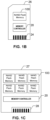
- memory controller 20 and a single NAND flash memory 100 can be integrated into a memory card 26.
- Memory card 26 can include a PC card (PCMCIA, personal computer memory card international association), a CF card, a smart media (SM) card, a memory stick, a multimedia card (MMC, RS-MMC, MMCmicro), an SD card (SD, miniSD, microSD, SDHC), a UFS, etc.
- Memory card 26 can further include a memory card connector 24 coupling memory card 26 with a host (e.g., the host computer 15 in FIG. 16).
- memory controller 20 and multiple NAND flash memories 100 can be integrated into a solid state drive (SSD) 27.
- SSD 27 can further include an SSD connector 28 coupling SSD 27 with a host (e.g., the host computer 15 in FIG. 1A ).
- the NAND flash memory 100 (i.e., “flash,” “NAND flash” or “NAND”) can be a memory chip (package), a memory die or any portion of a memory die, and can include one or more memory planes 101, each of which can include a plurality of memory blocks 103. Identical and concurrent operations can take place at each memory plane 101.
- the memory block 103 which can be megabytes (MB) in size, is the smallest size to carry out erase operations. Shown in FIG. 1A , the exemplary NAND flash memory 100 includes four memory planes 101 and each memory plane 101 includes six memory blocks 103.
- Each memory block 103 can include a plurality of memory cells, where each memory cell can be addressed through interconnections such as bit lines and word lines.
- the bit lines and word lines can be laid out perpendicularly (e.g., in rows and columns, respectively), forming an array of metal lines.
- the direction of bit lines and word lines are labeled as "BL” and "WL” respectively in FIG. 1A .
- one or more memory block 103 can also be referred to as the "memory array" or “array.”
- the memory array is the core area in a memory device, performing storage functions.
- the NAND flash memory 100 also includes a peripheral circuit region 105, an area surrounding memory planes 101.
- the peripheral circuit region 105 also named as peripheral circuits, contains many digital, analog, and/or mixed-signal circuits to support functions of the memory array, for example, page buffers/sense amplifiers 50, row decoders/word line drivers 40, column decoders/bit line drivers 60, and control circuits 70.
- Control circuits 70 include register, active and/or passive semiconductor devices, such as transistors, diodes, capacitors, resistors, etc., as would be apparent to a person of ordinary skill in the art.
- the control circuits 70 of the peripheral circuit region 105 can be configured to initiate a program operation on a select memory cell of a NAND memory string in the memory block 103.
- control circuits 70 receives a program command from a memory controller (e.g., memory controller 20) through interface, and in response, sends control signals to at least row decoder/word line driver, column decoder/bit line driver, and voltage generator deposed in the peripheral circuit region 105 to initiate the program operation on the select memory cell.
- a memory controller e.g., memory controller 20
- the layout of the electronic components in the memory system 10 and the NAND flash memory 100 in FIG. 1A are shown as an example.
- the memory system 10 and the NAND flash memory 100 can have other layout and can include additional components.
- the NAND flash memory 100 can also have high-voltage charge pumps, I/O circuits, etc.
- the memory system 10 can also include firmware, data scrambler, etc.
- the peripheral circuit region 105 and the memory array can be formed independently on separate wafers and then connected with each other through wafer bonding.
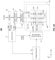
- FIG. 2A shows a schematic diagram of the NAND flash memory 100, according to some embodiments of the present disclosure.
- the NAND flash memory 100 includes one or more memory blocks 103.
- Each memory block 103 includes memory strings 212.
- Each memory string 212 includes memory cells 340.
- the memory cells 340 sharing the same word line forms a memory page 448.
- the memory string 212 can also include at least one field effect transistor (e.g., MOSFET) at each end, which is controlled by a bottom select gate (BSG) 332 and a top select gate (TSG) 334, respectively.
- the drain terminal of a top select transistor 334-T can be connected to the bit line 341, and the source terminal of a bottom select transistor 332-T can be connected to an array common source (ACS) 446.
- the ACS 446 can be shared by the memory strings 212 in an entire memory block, and is also referred to as the common source line.
- the NAND flash memory 100 can also include a peripheral circuit that includes many digital, analog, and/or mixed-signal circuits to support functions of the memory block 103, for example, a page buffer/sense amplifier 50, a row decoder/word line driver 40, a column decoder/bit line driver 60, a control circuit 70, a voltage generator 65 and an input/output buffer 55.
- peripheral circuit can include active and/or passive semiconductor devices, such as transistors, diodes, capacitors, resistors, etc., as would be apparent to a person of ordinary skill in the art.
- the peripheral circuit can support an erase operation assisted by a gate-induced drain leakage (GIDL) current.
- GIDL gate-induced drain leakage
- the memory blocks 103 can be coupled with the row decoder/word line driver 40 via word lines ("WLs”) 333, bottom select gates (“BSGs”) 332 and top select gates (“TSG”) 334.
- the memory blocks 103 can be coupled with the page buffer/sense amplifier 50 via bit lines ("BLs") 341.
- the row decoder/word line driver 40 can select one of the memory blocks 103 on the NAND flash memory 100 in response to an X-path control signal provided by the control circuit 70.
- the row decoder/word line driver 40 can transfer voltages provided from the voltage generator 65 to the word lines according to the X-path control signal.
- the row decoder/word line driver 40 can transfer a read voltage V read and a program voltage V pgm to a selected word line and a pass voltage V pass to an unselected word line according to the X-path control signal received from the control circuit 70.
- the column decoder/bit line driver 60 can transfer an inhibit voltage V inhibit to an unselected bit line and connect a selected bit line to ground according to a Y-path control signal received from the control circuit 70.
- the column decoder/bit line driver 60 can be configured to select or unselect one or more memory strings 212 according to the Y-path control signal from the control circuit 70.
- the page buffer/sense amplifier 50 can be configured to read and program (write) data from and to the memory block 103 according to the control signal Y-path control from the control circuit 70.
- the page buffer/sense amplifier 50 can store one page of data to be programmed into one memory page 448.
- page buffer/sense amplifier 50 can perform verify operations to ensure that the data has been properly programmed into each memory cell 340.
- the page buffer/sense amplifier 50 can sense current flowing through the bit line 341 that reflects the logic state (i.e., data) of the memory cell 340 and amplify small signal to a measurable magnification.
- the input/output buffer 55 can transfer the I/O data from/to the page buffer/sense amplifier 50 as well as addresses ADDR or commands CMD to the control circuit 70.
- the input/output buffer 55 can function as an interface between the memory controller 20 (in FIG. 1A ) and the NAND flash memory 100.
- the control circuit 70 can control the page buffer/sense amplifier 50 and the row decoder/word line driver 40 in response to the commands CMD transferred by the input/output buffer 55. During the programming operation, the control circuit 70 can control the row decoder/word line driver 40 and the page buffer/sense amplifier 50 to program a selected memory cell. During the read operation, the control circuit 70 can control the row decoder/word line driver 40 and the page buffer/sense amplifier 50 to read a selected memory cell.
- the X-path control signal and the Y-path control signal include a row address X-ADDR and a column address Y-ADDR that can be used to locate the selected memory cell in the memory block 103.
- the row address X-ADDR can include a page index, a block index and a plane index to identify the memory page 448, memory block 103, and memory plane 101 (in FIG. 1A ), respectively.
- the column address Y-ADDR can identify a byte or a word in the data of the memory page 448.
- control circuit 70 can include one or more control logic unit.
- Each control logic unit described herein can be either a software module and/or a firmware module running on a processor, such as a microcontroller unit (MCU), which is part of control circuits 70, or a hardware module of a finite-state machine (FSM), such as an integrated circuit (IC, e.g., application-specific IC (ASIC), field-programmable gate array (FPGA), etc.), or a combination of software module, firmware module, and hardware module.
- MCU microcontroller unit
- FSM finite-state machine
- IC integrated circuit
- ASIC application-specific IC
- FPGA field-programmable gate array
- the voltage generator 65 can generate voltages to be supplied to word lines and bit lines under the control of the control circuit 70.
- the voltages generated by the voltage generator 65 include the read voltage V read , the program voltage V pgm , the pass voltage V pass , the inhibit voltage V inhibit , etc.
- the NAND flash memory 100 can be formed based on the floating gate technology. In some embodiments, the NAND flash memory 100 can be formed based on charge trapping technology. The NAND flash memory based on charge trapping can provide high storage density and high intrinsic reliability. Storage data or logic states (e.g., threshold voltage V th of the memory cell 340) depends on the amount of charge trapped in a storage layer. In some embodiments, the NAND flash memory 100 can be a three-dimensional (3D) memory device, where the memory cells 340 can be vertically stacked on top of each other.
- 3D three-dimensional
- FIG. 2B illustrates a perspective view of a portion of a 3D NAND flash memory 200, according to some embodiments of the present disclosure.
- the 3D NAND flash memory 200 includes a substrate 330, an insulating film 331 over the substrate 330, a tier of bottom select gates (BSGs) 332 over the insulating film 331, and tiers of control gates 333, also referred to as "word lines (WLs),” stacking on top of the BSGs 332 to form a film stack 335 of alternating conductive and dielectric layers.
- the dielectric layers adjacent to the tiers of control gates are not shown in FIG. 2B for clarity.
- the control gates of each tier are separated by slit structures 216-1 and 216-2 through the film stack 335.
- the 3D NAND flash memory 200 also includes a tier of top select gates (TSGs) 334 over the stack of control gates 333.
- the stack of TSG 334, control gates 333 and BSG 332 is also referred to as "gate electrodes".
- the 3D NAND flash memory 200 further includes memory strings 212 and doped source line regions 344 in portions of substrate 330 between adjacent BSGs 332.
- Each memory strings 212 includes a channel hole 336 extending through the insulating film 331 and the film stack 335 of alternating conductive and dielectric layers.
- Memory strings 212 also includes a memory film 337 on a sidewall of the channel hole 336, a channel layer 338 over the memory film 337, and a core filler 339 surrounded by the channel layer 338.
- a memory cell 340 e.g., 340-1, 340-2, 340-3) can be formed at the intersection of the control gate 333 (e.g., 333-1, 333-2, 333-3) and the memory string 212.
- a portion of the channel layer 338 responds to the respective control gate is also referred to as the channel layer 338 of the memory cell.
- the 3D NAND flash memory 200 further includes bit lines (BLs) 341 connected with the memory strings 212 over the TSGs 334.
- the 3D NAND flash memory 200 also includes metal interconnect lines 343 connected with the gate electrodes through contact structures 214.
- the edge of the film stack 335 is configured in a shape of staircase to allow an electrical connection to each tier of the gate electrodes.
- each memory string 212 can include three memory cells 340-1, 340-2 and 340-3, corresponding to the control gates 333-1,333-2 and 333-3, respectively.
- the number of control gates and the number of memory cells can be more than three to increase storage capacity.
- the 3D NAND flash memory 200 can also include other structures, for example, TSG cut, common source contact, array common source and dummy memory string. These structures are not shown in FIG. 2B for simplicity.
- a NAND flash memory In a NAND flash memory, read and programming operations can be performed in a memory page 448, which includes all memory cells 340 sharing the same word line.
- the memory cell 340 In a NAND memory, the memory cell 340 can be in an erased state ER or a programmed state P1.
- a memory cell can store n -bit of data and have 2 n states, where n is a whole number. For example, n equals 1, 2, 3, and 4 for SLC, MLC, TLC and QLC mode, respectively.
- all memory cells 340 in the same memory block 103 can be reset to the erased state ER as logic "1" by implementing a negative voltage difference between the control gates 333 and source terminals of the memory cells (e.g., the array common source 446) such that all the trapped electronic charges in the storage layer of the memory cells 340 can be removed.
- the negative voltage difference can be induced by setting the control gates 333 of the memory cells 340 to ground, and applying a high positive voltage to the array common source 446.
- an incremental step pulse erase (ISPE) scheme can be used for the erase operation.
- a voltage pulse can be applied to the memory cells in an erase loop, where a magnitude of the voltage pulse, i.e., the erase voltage V erase , can be increased incrementally by an erase step voltage V step_ers in subsequent erase loops.
- an erase verification operation can be performed to determine if the memory cells are at the state ER, or if the erase operation is completed successfully.
- An erase verification voltage EV can be applied to the word lines of the memory cells to compare with the threshold voltages of the memory cells. If the erase verification voltage EV is higher than the threshold voltage of the memory cell, it can be determined that the memory cell is at the state ER. If all the memory cells in the memory block are at the state ER, it can be considered that the memory block passes the erase verification. If a predetermined number of memory cell are not at the state ER, it can be considered that the memory block fails the erase verification.
- the erase and erase verification operations can be performed for the memory cells again in a next erase loop, where the erase voltage V erase can be increased by the erase step voltage V step_ers .
- the erase voltage V erase can be applied to an n-well in the substrate that is shared by all the memory cells in the same memory block.
- the erase voltage V erase can be applied to the ACS 446 as shown in FIG. 2A .
- the NAND flash memory 100 can have a three-dimensional structure, for example, as the 3D NAND flash memory 2000 shown in FIG. 2B .
- the NAND flash memory can also include an additional transistor at each end of the memory string, where the additional transistor introduces gate-induced drain leakage (GIDL) to assist the erase operation.
- GIDL gate-induced drain leakage
- FIG. 3 illustrates a 3D NAND flash memory 300, according to some embodiments of the present disclosure.
- the 3D NAND flash memory 300 can be a portion of a memory block 103 in FIG. 1A . Similar to the 3D NAND flash memory 200 in FIG. 2B , the 3D NAND flash memory 300 also includes the film stack 335 of alternating conductive and dielectric layers and a plurality of memory strings 212 having a plurality of vertically stacked memory cells 340.
- the word lines 333 for all the memory cells 340 in the same memory block can be grounded, and the erase voltage V erase can be applied to the bit lines 341 on top of the memory strings 212 and to a source line (SL) 342 at bottom of the memory strings.
- the SL 342 can be shared by all the memory strings 212 and all the memory cells 340 in the same memory block. In one example, the SL 342 can be connected to the ACS 446.
- the SL 342 can be coupled to the channel layer 338 of the memory string 212 through a SL contact 350.
- the bit line (BL) 341 can be coupled to the channel layer 338 through a BL contact 352.
- the SL contact 350 and the BL contact 352 comprise polycrystalline silicon.
- the SL contact 350 and the BL contact 352 can be doped with an n-type dopant, for example, phosphine or arsenic.
- the 3D NAND flash memory 300 also includes multiple select gates, for example, BSG 332-1, BSG 332-2, TSG 334-1 and TSG 334-2, where at least one select gate (e.g., BSG 332-2 and TSG 334-2) at each end of the memory string 212 can be controlled such that a GIDL current can be generated and charge carriers (e.g., holes) can be injected from the SL 342 and the BL 341 to the channel layer 338 during an erase operation.
- charge carriers e.g., holes
- a negative voltage bias between the word line 333 and corresponding channel layer 338 can remove trapped charge carriers (e.g., electrons) in the memory film 337 and thereby reduce the threshold voltage of corresponding memory cell 340.
- the erase and erase verification operation complete i.e., after the memory cell is reset to the erase state ER, the stored data in the memory cell are erased accordingly.
- the erase operation can be assisted by the gate-induced-drain-leakage (GIDL) current flowing through the bit line and the source line of the memory device.
- GIDL gate-induced-drain-leakage
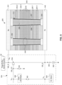
- FIG. 3 also illustrates a first discharge circuit 302 for a 3D NAND flash memory, according to some embodiments of the present disclosure.
- the first discharge circuit 302 can be a portion of the peripheral circuit shown in FIG. 2A and can be fabricated in the peripheral region.
- the first discharge circuit 302 can be coupled to the 3D NAND flash memory 300 to discharge the 3D NAND flash memory 300, for example, the bit line 341 and the SL 342, after an erase operation.
- the first discharge circuit 302 includes a discharge transistor 354.
- the discharge transistor 354 can be a metal-oxide-semiconductor field-effect-transistor (MOSFET). In some embodiments, the discharge transistor 354 can be an n-channel MOSFET.
- a drain terminal (DS_D) of the discharge transistor 354 can be connected to the BL 341, which can be connected to its corresponding page buffer/sense amplifier 50.
- a source terminal (DS_S) of the discharge transistor 354 can be connected to the SL 342, which can be connected to the ACS 446 and a current source 360 via a first switch 356.
- the current source 360 can be used to regulate a discharge current flowing through to ground. In some embodiments, the current source 360 can be a flexible limited current source.
- a gate terminal (DS_GT) of the discharge transistor 354 can be grounded via a second switch 358.
- the discharge transistor 354 can be included as a component in the page buffer/sense amplifier 50.
- each BL 341 is connected to one discharge transistor 354 at its drain terminal DS_D. All the discharge transistors 354 in the entire memory block can be connected at the source terminals DS_S to the shared SL 342.
- the gate terminals DS_GT of all the discharge transistors 354 in the same memory block can also be connected together to the second switch 358.
- FIGs. 4A and 4B illustrate waveforms 400A and 400B used for erase and discharge operations of a 3D NAND flash memory, according to some embodiments of the present disclosure.
- Each erase operation is followed by the discharge operation.
- the first switch 356 can be switched off, and the erase voltage V erase can be applied to the SL 342.
- the gate terminal DS_GT of the discharge transistor 354 can be applied with a switch-on voltage VGG to switch on the discharge transistor 354 such that the source terminal DS_S and the drain terminal DS_D of the discharge transistor 354 are electrically connected.
- the BL 341 is thereby also connected to the source terminal DS_S and the SL 342, and is applied with the erase voltage V erase .
- the erase voltage V erase can be in a range between about 18 V to about 22 V.
- the switch-on voltage VGG is higher than the erase voltage V erase applied on the source terminal DS_S.
- the switch-on voltage VGG can be in a range between about 22 V to about 27 V.
- each BL 341 is connected to one discharge transistor 354, the plurality of discharge transistors 354 can be switched on during the erase operation such that the plurality of bit lines 341 can be connected to the source line 342 during the erase operation, where the plurality of bit lines 341 and the source line 342 can be applied with the erase voltage V erase during the erase operation.
- the gate-induced-drain-leakage (GIDL) current can flow through each bit line and the source line into the channel layer of each memory string to assist the erase operation.
- the first switch 356 can be switched on such that the source terminal DS_S of the discharge transistor 354 can be grounded through the current source 360, for example a flexible limited current source.
- the current source 360 can regulate the discharge current flowing through and thereby regulate the discharge rate of the SL 342.
- an electrical potential V SL of the SL 342 can be reduced to 0 V.
- the BL 341 can be connected to the SL 342 and ground when the discharge transistor 354 is switched on. Namely, the BL 341 can be discharged simultaneously with the SL 342 through the discharge transistor 354.
- the discharge transistor 354 can be switched off by switching on the second switch 358 to connect the gate terminal DS_GT to ground.
- timing of switching off the discharge transistor 354 during the discharge operation can impact the performance and reliability of the discharge transistor 354.
- the second switch 358 is switched on at the same time when the first switch 356 is switched on. Because the gate terminal DS_GT is grounded when the second switch 358 is switched on, the discharge transistor 354 can be switched off. In this example, an electrical potential V BL of the BL 341 is still at a high level (e.g., close to the erase voltage V erase ) when the discharge transistor 354 is switched off. Because the fast discharge path through the discharge transistor 354 is turned off, the electrical potential V BL of the BL 341 remains at the high level, as shown in waveform 400A.
- the drain terminal DS-D of the discharge transistor 354 is connected to the BL 341, the drain terminal DS-D of the discharge transistor 354 and the BL 341 are at the same electrical potential V BL . Therefore, after the SL 342 drops to 0 V, there is a high electrical potential difference between the drain terminal DS_D and the source terminal DS_S of the discharge transistor 354, which can cause breakdown of source/drain junctions. As the discharge transistor 354 is scaled down to a smaller dimension, a source/drain breakdown voltage of the discharge transistor 354 is decreasing. Therefore, if switching off the discharge transistor 354 too early, the high electrical potential difference between source and drain terminals can cause breakdown of the source/drain junctions of the discharge transistor 354.
- the second switch 358 is switched on when the SL 342 is dropping to 0 V.
- the discharge transistor 354 remains switching on when the electrical potential V SL of the SL 342 is decreasing from the erase voltage V erase to 0 V. Because the BL 341 is electrically connected to the SL 342 through the discharge transistor 354 when the discharge transistor 354 is switched on, the electrical potential V BL of the BL 341 follows the electrical potential V SL of the SL 342 and drops to 0 V at the same discharge rate.
- the source and drain of the discharge transistor 354 are at the same electrical potential in this example, there is a large voltage difference between the gate terminal DS_GT and the source/drain terminal DS_S/DS_D, which can induce Fowler-Nordheim (FN) stress to a gate dielectric of the discharge transistor 354.
- FN Fowler-Nordheim
- a threshold voltage of the discharge transistor 354 can increase accordingly, and performance and reliability of the discharge transistor 354 can decrease as a result.
- FIG. 5 illustrates a second discharge circuit 504 for a 3D NAND flash memory, according to some embodiments of the present disclosure.
- the second discharge circuit 504 is similar to the first discharge circuit 302, and can be coupled to the 3D NAND flash memory 300. The difference and improvement of the second discharge circuit 504 over the first discharge circuit 302 will be described in detail below.
- the second discharge circuit 504 also includes a SL detect circuit 564, which is connected to the SL 342 and the source terminal DS_S of the discharge transistor 354.
- the SL detect circuit 564 is further connected to the current source 360 (e.g., a flexible limited current source) via the first switch 356.
- the second discharge circuit 504 also includes a gate discharge circuit 566, which is connected to the gate terminal DS_GT of the discharge transistor 354.
- the gate discharge circuit 566 is also connected to the SL detect circuit 564 via a third switch 562.
- FIG. 6 illustrates a waveform 600 used for the second discharge circuit 504, according to some embodiments of the present disclosure.
- the waveform 600 depicts the erase and discharge operations performed to the 3D NAND flash memory 300 with the support from the second discharge circuit 504.
- the erase operation represented by the waveform 600 is also followed by the discharge operation.
- the erase operation of the waveform 600 is similar to waveforms 400A and 400B, as described with respect to FIGs. 4A and 4B .
- timing for discharging the gate terminal DS_GT of the discharge transistor 354 can be controlled through the second discharge circuit 504 such that the discharge transistor 354 will not suffer FN stress or source/drain junction breakdown.
- FIG. 7 illustrates a method 700 for discharging a 3D NAND flash memory after an erase operation, according to some embodiments of the present disclosure. It should be understood that the method 700 is not exhaustive and that other operation steps can be performed as well before, after, or between any of the illustrated operation steps. In some embodiments, some operation steps of method 700 can be omitted or other operation steps can be included, which are not described here for simplicity. In some embodiments, operation steps of method 700 can be performed in a different order and/or vary.
- the following operation steps can be implemented as an example for discharging the 3D NAND flash memory 300 through the second discharge circuit 504 after the erase operation.
- the erase voltage V erase can be applied to the SL 342.
- the switch-on voltage VGG can be applied to the gate terminal DS_GT of the discharge transistor 354 to switch on the discharge transistor 354.
- the BL 341 can be connected to the SL 342 and can also be applied with the erase voltage V erase .
- the erase voltage V erase and the switch-on voltage VGG can be removed from the SL 342 and the gate terminal DS_GT, respectively.
- the SL 342 can be grounded by switching on the first switch 356. In the other words, a zero volt (0 V) can be applied to the SL 342.
- the source terminal DS_S of the discharge transistor 354 is connected to the SL 342 and thereby the source terminal DS_S of the discharge transistor 354 is kept at the same electrical potential V SL and is discharged simultaneously with the SL 342.
- the current source 360 connected between the first switch 356 and the ground, can regulate the discharge current flowing through and thereby regulate the discharge rate of the SL 342.
- the current source 360 can be a flexible limited current source. As shown in FIG. 6 , the electrical potential V SL of the SL 342 drops from the erase voltage V erase at the time T0 to 0 V at the end of the discharge operation with a slope representing its discharge rate.
- the third switch 562 can be switch on at the same time as the first switch 356, i.e., at the time T0, to form an electrical connection from the gate terminal DS_GT of the discharge transistor 354 to the SL 342 through the gate discharge circuit 566.
- a constant voltage difference Vg_Vs can be provided and maintained between the gate terminal DS_GT of the discharge transistor 354 and the SL 342 by the gate discharge circuit 566.
- the constant voltage difference Vg_Vs can be higher than the threshold voltage of the discharge transistor 354 such that the discharge transistor 354 can be switched on.
- the constant voltage difference Vg_Vs can be in a range between about 3 V to about 10 V.
- the constant voltage difference Vg_Vs is 5 V.
- the constant voltage difference Vg_Vs can be selected to remain smaller an FN stress voltage, for example, 15 V.
- the BL 341 and the gate terminal DS_GT can be discharged at the same discharge rate as the SL 342.
- an electrical potential V GT of the gate terminal DS_GT and the electrical potential V BL of the BL 341 drop from the switch-on voltage VGG and the erase voltage V erase , respectively, at the time T0, with the same slope as the SL 342. Because the BL 341 and the SL 342 are electrically connected at about the same electrical potential, source/drain junction breakdown can also be avoided during this period.
- the electrical potential V SL of the SL 342 can be compared with a first predetermined value VF1 by the SL detect circuit 564.
- the first predetermined value VF1 can be selected in a range between, for example, 3V and 5V.
- step S740 it is determined whether the electrical potential V SL of the SL 342 is smaller or lower than the first predetermined value VF1. If the electrical potential V SL of the SL 342 is not lower than the first predetermined value VF1, the operation steps S720 and S730 can be repeated.
- the third switch 562 can be switched off according to operation step S750.
- the gate terminal DS_GT of the discharge transistor 354 can be floating. Namely, there is no external bias applied on the gate terminal DS_GT. Due to capacitive coupling effect, the electrical potential V GT of the gate terminal DS_GT follows the electrical potential V SL of the SL 342. The gate terminal DS_GT continues discharging, but at a discharge rate slower than the SL 342. In the meantime, the discharge transistor 354 remains switched-on such that the BL 341 can continue to be discharged through the discharge transistor 354.
- the electrical potential V SL of the SL 342 can be compared with a second predetermined value VF2 by the SL detect circuit 564.
- step S770 it is determined whether the electrical potential V SL of the SL 342 is smaller or lower than the second predetermined value VF2. If the electrical potential V SL of the SL 342 is not lower than the second predetermined value VF2, the operation steps S750 and S760 can be repeated.
- the second switch 358 can be switched on according to operation step S780.
- the gate terminal DS_GT is grounded, i.e., is applied with 0V.
- the gate terminal DS_GT can thus be quickly discharged to 0V.
- the discharge transistor 354 is switched off accordingly.
- the second predetermined value VF2 can be smaller than the first predetermined valve VF1. In some embodiments, to avoid source/drain junction breakdown, the second predetermined value VF2 can be selected to below a source/drain junction breakdown voltage. In some embodiments, the second predetermined value VF2 can be between 0.5V and 3V, for example, e.g. the second predetermined value VF2 can be 1V or 2V. Therefore, even after the discharge transistor 354 is switched off, without a quick discharge path, the electrical potential V BL of the BL 341 can be controlled to below the source/drain junction breakdown voltage.
- the first, second and third switches 356/358/562 in the second discharge circuit 504 can be switched off.
- FIGs. 8A and 8B illustrate schematic diagrams 800A and 800B of the gate discharge circuit 566, according to some embodiments of the present disclosure.
- the gate discharge circuit 566 can maintain the constant voltage different Vg_Vs between the electrical potential V GT of the gate terminal DS_GT and the electrical potential V SL of the SL 342 shown in FIG. 5 .
- the gate discharge circuit 566 can be designed in the peripheral circuit of a 3D NAND flash memory.
- the gate discharge circuit 566 includes a switch transistor 872 and a voltage level shifter 874.
- a source terminal of the switch transistor 872 can be connected to the SL 342 (not shown in FIG. 8A ) at the electrical potential V SL .
- the third switch 562 can be inserted between the SL 342 and the gate discharge circuit 566.
- the switch transistor 872 can be implemented as the third switch 562.
- the switch transistor 872 can be implemented in addition to the third switch 562.
- the switch transistor 872 can be switched on or off through the voltage level shifter 874 connected to a gate terminal of the switch transistor 872.
- the voltage level shifter 874 can transform the electrical potential V GT at the gate terminal DS_GT of the discharge transistor 354 to a switching voltage Vsw for switching on the switch transistor 872.
- the voltage level shifter 874 can also be controlled by an enablement signal dis_en to determine when the switching voltage Vsw can be provided to the switching transistor 872.
- a switching current I SW flowing through the switching transistor 872 can be determined by the switching voltage Vsw.
- the gate discharge circuit 566 also includes a set of MOSFETs 870 connected in series.
- a first end of the set of MOSFETs 870 can be connected to a drain terminal of the switching transistor 872 and a second end of the set of MOSFETs 870 can be connected to the gate terminal DS_GT of the discharge transistor 354 at the electrical potential V GT .
- Each of the set of MOSFETs 870 can be configured as an effective diode - a gate terminal can be connected to a drain terminal. As such, each of the set of MOSFETs can operation in its saturation mode. A voltage drop across each of the set of MOSFETs 870 depends on the switching current I SW which is controlled by the switching transistor 872.
- a total voltage drop across the set of MOSFETs 870 from the first end to the second end can determine the constant voltage difference Vg_Vs between the electrical potentials V GT and V SL .
- each of the set of MOSFETs 870 can be bypassed by a parallel switch (e.g, switch S1, S2, ...) such that the constant voltage difference Vg_Vs between the electrical potentials V GT and V SL can be adjusted.
- the set of MOSFETs 870 can include p-channel MOSFETs or n-channel MOSFETs.
- p-channel MOSFETs are illustrated as an example.
- a body of each MOSFET can be tied to a source terminal of the MOSFET. Since the body of a p-channel MOSFET is in an n-well and can be tied to its source terminal easily, it is preferred that p-channel MOSFETs can be used in the set of MOSFETs 870 instead of n-channel MOSFETs.
- the gate discharge circuit 566 can also include a set of diodes 876 connected in series.
- a first end of the set of diodes 876 can be connected to the drain terminal of the switching transistor 872, and a second end of the set of diodes 876 can be connected to the gate terminal DS_GT of the discharge transistor 354 at the electrical potential V GT .
- a voltage drop across each of the set of diodes 876 depends on the switching current I SW that is controlled by the switching transistor 872.
- a total voltage drop across the set of diodes 876 from its first end to the second end can determine the constant voltage difference Vg_Vs between the electrical potentials V GT and V SL .
- each of the set of diodes 876 can also be bypassed by the parallel switch (e.g, switch S1, S2, ...) such that the constant voltage difference Vg_Vs between the electrical potentials V GT and V SL can be adjusted.
- the parallel switch e.g, switch S1, S2, .
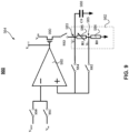
- FIG. 9 illustrates a schematic diagram 900 of the SL detect circuit 564, according to some embodiments of the present disclosure.
- the SL detect circuit 564 can compare the electrical potential V SL of the SL 342 with a predetermined value (e.g., the first predetermined value VF1 or the second predetermined value VF2).
- a predetermined value e.g., the first predetermined value VF1 or the second predetermined value VF2.
- the SL detect circuit 564 includes an operational amplifier 980, which has a negative input and a positive input.
- the negative input of the operational amplifier 980 can be connected to a reference voltage V REF or a input voltage V IN .
- Switches SS0 and SS1 can be used to select the reference voltage V REF or the input voltage V IN .
- the operational amplifier 980 is a comparator.
- the SL detect circuit 564 also includes a resistive voltage divider 982 that has a first resistor 984 connected in series with a second resistor 986.
- the first resistor 984 has a resistance R0 and the second resistor 986 has a resistance R1 that can be adjusted.
- the second resistor 986 is a potentiometer.
- the resistive voltage divider 982 is connected in parallel with a capacitor 988, where first ends 983 of the resistive voltage divider 982 and the capacitor 988 are connected together to the positive input of the operational amplifier 980 via a switch SS4. Second ends of the resistive voltage divider 982 and the capacitor 988 are both grounded.
- the capacitor 988 has a capacitance C 0 .
- An intermediate point 985 between the first resistor 984 and the second resistor 986 is connected to the positive input of the operational amplifier 980 via a switch SS2.
- the SL detect circuit 564 also includes a pull-up transistor 990.
- the pull-up transistor 990 is a p-channel MOSFET, where a drain terminal of the pull-up transistor 990 is connected to the first ends of the resistive voltage divider 982 and the capacitor 988 via a switch SS3, and a source terminal of the pull-up transistor 990 is connected to a power supply V DD .
- a gate terminal of the pull-up transistor 990 is connected to an output of the comparator with an output voltage V OUT .
- the predetermined value (e.g., the first predetermined value VF 1 and the second predetermined value VF2) used in the method 700 for the discharge operation can be set to the SL detect circuit 564.
- the input voltage V IN e.g., the electrical potential V SL of the SL 342
- V SL the electrical potential of the SL 342
- FIG. 10 illustrates a method 1000 to set the predetermined value (e.g., the first predetermined value VF 1 or the second predetermined value VF2) to the SL detect circuit 564, according to some embodiments of the present disclosure.
- the method 1000 is not exhaustive and that other operation steps can be performed as well before, after, or between any of the illustrated operation steps. In some embodiments, some operation steps of method 1000 can be omitted or other operation steps can be included, which are not described here for simplicity. In some embodiments, operation steps of method 1000 can be performed in a different order and/or vary.
- the switch SS0 can be switched on, and the switch SS1 can be switched off.
- the negative input of the operational amplifier 980 is at the reference voltage V REF .
- the switches SS2 and SS3 can be switched on, and the switch SS4 can be switched off.
- the positive input of the operational amplifier 980 is connected to the intermediate point 985 of the resistive voltage divider 982, which is at an electrical potential V 0 .
- the electrical potential V 1 can be set to the predetermined value, for example, the first predetermined value VF1 or the second predetermined value VF2.
- the capacitor 988 connected in parallel with the resistive voltage divider 982, is charged to the electrical potential V1 through the pull-up transistor 990 and the power supply V DD . Accordingly, the electrical potential V1, i.e., the first predetermined value VF1 or the second predetermined value VF2, can be held by the capacitor 988 once the power supper V DD is disconnected.
- the operational amplifier 980 is configured as a voltage buffer, where an input voltage can be mirrored or followed at an output.
- FIG. 11 illustrates a method 1100 to compare the input voltage V IN (e.g., the electrical potential V SL of the SL 342) with the predetermined value (i.e., the electrical potential V1, e.g., the first predetermined value VF1 or the second predetermined value VF2), according to some embodiments of the present disclosure.
- V IN the electrical potential
- V1 the electrical potential
- V2 the electrical potential
- the switches SS2 and SS3 can be switched off, and the switches SS4 can be switched on.
- the electrical potential V1 e.g., the first predetermined value VF1 or the second predetermined value VF2
- the capacitor 988 can be connected to the positive input of the operational amplifier 980.
- the switch SS0 can be switched off and the switch SS1 can be switched on. Accordingly, the input voltage V IN can be connected to the negative input of the operational amplifier 980.
- the input voltage V IN can be compared with the electrical potential V1 by the operational amplifier 980.
- the operational amplifier 980 is configured as a comparator, where voltages at its two inputs can be compared.
- step 1140 it is determined whether the input voltage V IN is lower than the electrical potential V1 or not.
- the output voltage V OUT can be positive or logic "1."
- the output voltage can be negative or logic "0.”
- the discharge operation for the 3D NAND flash memory can be optimized.
- the discharge transistor 354 remains switched on to discharge the BL 342.
- a high voltage difference between the source terminal DS_S and the drain terminal DS_D can be avoided.
- source/drain junction breakdown of the discharge transistor 354 can be avoided.
- the constant voltage difference Vg_Vs can also be used to avoid causing FN stress to the gate dielectric of the discharge transistor 354.
- source/drain junction breakdown or FN stress can also be avoided by comparing the electrical potential V SL of the SL 342 with the first predetermined value VF1 and the second predetermined value VF2.
- discharging methods and circuits described in the present disclosure are not limited to a three-dimensional NAND flash memory or a NAND flash memory. Any system having a discharge operation can adapt the methods and circuits described above to achieve improved performance and reliability.
- the present disclosure provides a discharge circuit for discharging a memory device after an erase operation.
- the discharge circuit includes a discharge transistor, connecting a bit line and a source line of the memory device.
- the discharge circuit also includes a source line detect circuit, connected to the source line and configured to compare an electrical potential of the source line with a predetermined value.
- the discharge circuit further includes a gate discharge circuit, configured to maintain a constant voltage difference between the discharge transistor and the source line, wherein the constant voltage difference applied to the discharge transistor and the source line switches on the discharge transistor.
- the present disclosure also provides a method for discharging a memory device after an erase operation.
- the method comprises grounding a source line of the memory device; and switching on a discharge transistor to connect a bit line of the memory device to the source line by maintaining a constant voltage difference between a gate terminal of the discharge transistor and the source line.
- the method also includes comparing an electrical potential of the source line with a first predetermined value; and floating the gate terminal of the discharge transistor when the electrical potential of the source line is lower than the first predetermined value.
- the present disclosure further provides a memory device having a memory block and a peripheral circuit.
- the memory block includes a plurality of memory strings connected to a source line and a plurality of bit lines.
- the peripheral circuit includes a discharge circuit configured to discharge the memory block after an erase operation.
- the discharge circuit includes a plurality of discharge transistors. Each discharge transistor is configured to connect the source line to a corresponding bit line.
- the discharge circuit also includes a source line detect circuit connected to the source line and configured to compare an electrical potential of the source line with a predetermined value.
- the discharge circuit further includes a gate discharge circuit, configured to maintain a constant voltage difference between gate terminals of the plurality of discharge transistors and the source line.
Landscapes
- Engineering & Computer Science (AREA)
- Microelectronics & Electronic Packaging (AREA)
- Physics & Mathematics (AREA)
- Computer Hardware Design (AREA)
- Computing Systems (AREA)
- General Engineering & Computer Science (AREA)
- Mathematical Physics (AREA)
- Read Only Memory (AREA)
- Semiconductor Memories (AREA)
- Non-Volatile Memory (AREA)
Claims (13)
- Eine löschbare Speichervorrichtung, umfassend:einen Speicherblock (103), der eine Vielzahl von Speicherstrings (212) umfasst, die mit einer Source-Leitung (342) und einer Vielzahl von Bit-Leitungen (341) verbunden sind; undeine Peripherieschaltung, die Folgendes umfasst:
eine Entladeschaltung (302, 504), die so konfiguriert ist, dass sie den Speicherblock (103) nach einer Löschoperation entlädt, wobei die Entladeschaltung (302, 504) umfasst:eine Vielzahl von Entladetransistoren (354), wobei jeder der Vielzahl von Entladetransistoren (354) so konfiguriert ist, dass er die Source-Leitung (342) mit einer entsprechenden Bit-Leitung (341) verbindet;eine Source-Leitungs-Erfassungsschaltung (564), die mit der Source-Leitung (342) verbunden ist und ein elektrisches Potential (VSL, VGT) der Source-Leitung (342) mit einem vorgegebenen Wert vergleicht; undeine Gate-Entladeschaltung (566), die eine konstante Spannungsdifferenz (Vg_Vs) zwischen Gate-Anschlüssen (DS_GT) der Vielzahl von Entladetransistoren (354) und der Source-Leitung (342) aufrechterhält,wobei die mehreren Entladetransistoren während des Löschvorgangs eingeschaltet werden, so dass die mehreren Bit-Leitungen mit der Source-Leitung verbunden sind. - Löschbare Speichervorrichtung nach Anspruch 1, wobei der Entladetransistor (354) ein Metall-Oxid-Halbleiter-Feldeffekttransistor (MOSFET) (870) ist, wobei der Gate-Anschluss (DS_GT) des MOSFET (870) mit der Gate-Entladeschaltung (566) verbunden ist, ein Source-Anschluss (DS_S) des MOSFET (870) mit der Source-Leitung (342) verbunden ist und ein Drain-Anschluss (DS_D) des MOSFET (870) mit der Bit-Leitung (341) verbunden ist.
- Löschbare Speichervorrichtung nach Anspruch 1, wobei die Gate-Entladeschaltung (566) einen Satz von in Reihe geschalteten Dioden (876) umfasst.
- Löschbare Speichervorrichtung nach Anspruch 3, wobei jede der Gruppe von Dioden (876) parallel mit einem Schalter (356, 358, 562) verbunden ist, so dass die konstante Spannungsdifferenz (Vg_Vs) einstellbar ist.
- Löschbare Speichervorrichtung nach Anspruch 3, wobei die Gate-Entladeschaltung (566) ferner einen Schalttransistor (872) umfasst, der in Reihe mit dem Satz von Dioden (876) geschaltet ist.
- Löschbare Speichervorrichtung nach Anspruch 5, wobei die Gate-Entladeschaltung (566) ferner einen Spannungspegelschieber (874) umfasst, der mit einem Gate-Anschluss des Schalttransistors (872) verbunden und so konfiguriert ist, dass er eine Schaltspannung (Vsw) bereitstellt, um den Schalttransistor (872) einzuschalten.
- Löschbare Speichervorrichtung nach Anspruch 3, wobei der Satz von Dioden (876) einen MOSFET (870) umfasst, der als eine effektive Diode (876) konfiguriert ist, wobei der Gate-Anschluss (DS_GT) des MOSFET (870) mit einem Drain-Anschluss (DS_D) des MOSFET (870) verbunden ist, wobei insbesondere der MOSFET (870) ein p-Kanal-MOSFET (870) ist.
- Löschbare Speichervorrichtung nach Anspruch 1, wobei die Source-Leitungs-Erfassungsschaltung (564) umfasst:einen Operationsverstärker (980);einen ohmschen Spannungsteiler (982); undeinen Kondensator (988), der parallel zu dem ohmschen Spannungsteiler (982) geschaltet ist,wobei:erste Enden des Kondensators (988) und des ohmschen Spannungsteilers (982) über einen Schalter (SS4) mit dem positiven Eingang des Operationsverstärkers (980) verbunden sind; undzweite Enden des Kondensators (988) und der Widerstandsspannungsteiler (982) geerdet sind.
- Löschbare Speichervorrichtung nach Anspruch 8, wobei die Source-Leitungs-Erfassungsschaltung (564) ferner einen Pull-up-Transistor (990) umfasst, der die ersten Enden des Kondensators (988) und des Widerstandsspannungsteilers (982) mit einer Stromversorgung (VDD) verbindet, wobei der Pull-up-Transistor (990) durch einen Ausgang des Operationsverstärkers (980) gesteuert wird
oder wobei der ohmsche Spannungsteiler (982) einen ersten Widerstand (984) umfasst, der mit einem zweiten Widerstand (986) in Reihe geschaltet ist, wobei ein Zwischenpunkt (985) zwischen dem ersten Widerstand (984) und dem zweiten Widerstand (986) über einen Schalter (SS2) mit dem positiven Eingang des Operationsverstärkers (980) verbunden ist, wobei der zweite Widerstand (986) einen einstellbaren Widerstand (R1) umfasst. - Löschbare Speichervorrichtung nach Anspruch 8, wobei der Operationsverstärker (980) so konfiguriert ist, dass er das elektrische Potential (VSL, VGT) der Source-Leitung (342) mit dem vorgegebenen Wert vergleicht, wobei:ein negativer Eingang des Operationsverstärkers (980) mit der Source-Leitung (342) verbunden ist; undein positiver Eingang des Operationsverstärkers (980) mit den ersten Enden des Kondensators (988) und dem ohmschen Spannungsteiler (982) verbunden ist.
- Löschbare Speichervorrichtung nach Anspruch 1, wobei die Source-Leitung (342) geerdet ist, wobei insbesondere eine Stromquelle (360) so ausgebildet ist, dass sie einen Entladestrom reguliert, der durch die Source-Leitung (342) fließt.
- Verfahren (700, 1000, 1100) zum Entladen einer löschbaren Speichervorrichtung nach einem der Ansprüche 1 bis 11 nach einem Löschvorgang, umfassend:Erden einer Source-Leitung (342) der Speichervorrichtung;Einschalten eines Entladetransistors (354), um eine Bit-Leitung (341) der Speichervorrichtung mit der Source-Leitung (342) zu verbinden, indem eine konstante Spannungsdifferenz (Vg_Vs) zwischen einem Gate-Anschluss (DS_GT) des Entladetransistors (354) und der Source-Leitung (342) aufrechterhalten wird;Vergleichen eines elektrischen Potentials (VSL, VGT) der Source-Leitung (342) mit einem ersten vorgegebenen Wert (VF1); undFloaten des Gate-Anschlusses (DS_GT) des Entladetransistors (354), wenn das elektrische Potential (VSL, VGT) der Source-Leitung (342) niedriger ist als der erste vorgegebene Wert (VF1),Vergleichen des elektrischen Potentials (VSL, VGT) der Source-Leitung (342) mit einem zweiten vorgegebenen Wert (VF2), wobei der zweite vorgegebene Wert (VF2) kleiner ist als der erste vorgegebene Wert (VF1),Erden des Gate-Anschlusses (DS_GT) des Entladetransistors (354), wenn das elektrische Potential (VSL, VGT) der Source-Leitung (342) niedriger als der zweite vorgegebene Wert (VF2) ist,
- Verfahren nach Anspruch 12, wobei der Löschvorgang durch einen Gate-induzierten Drain-Leckstrom (GIDL) unterstützt wird, der durch die Bit-Leitung (341) und die Source-Leitung (342) der Speichervorrichtung fließt.
Priority Applications (1)
| Application Number | Priority Date | Filing Date | Title |
|---|---|---|---|
| EP24195631.7A EP4443747A3 (de) | 2022-02-18 | 2022-02-18 | Entladeschaltungen für einen nand-flash-speicher |
Applications Claiming Priority (1)
| Application Number | Priority Date | Filing Date | Title |
|---|---|---|---|
| PCT/CN2022/076858 WO2023155139A1 (en) | 2022-02-18 | 2022-02-18 | Discharge circuits for a nand flash memory |
Related Child Applications (2)
| Application Number | Title | Priority Date | Filing Date |
|---|---|---|---|
| EP24195631.7A Division EP4443747A3 (de) | 2022-02-18 | 2022-02-18 | Entladeschaltungen für einen nand-flash-speicher |
| EP24195631.7A Division-Into EP4443747A3 (de) | 2022-02-18 | 2022-02-18 | Entladeschaltungen für einen nand-flash-speicher |
Publications (3)
| Publication Number | Publication Date |
|---|---|
| EP4252233A1 EP4252233A1 (de) | 2023-10-04 |
| EP4252233A4 EP4252233A4 (de) | 2023-10-11 |
| EP4252233B1 true EP4252233B1 (de) | 2024-10-16 |
Family
ID=87574788
Family Applications (2)
| Application Number | Title | Priority Date | Filing Date |
|---|---|---|---|
| EP24195631.7A Pending EP4443747A3 (de) | 2022-02-18 | 2022-02-18 | Entladeschaltungen für einen nand-flash-speicher |
| EP22817514.7A Active EP4252233B1 (de) | 2022-02-18 | 2022-02-18 | Nand-flash speicher mit einer entladungsschaltung |
Family Applications Before (1)
| Application Number | Title | Priority Date | Filing Date |
|---|---|---|---|
| EP24195631.7A Pending EP4443747A3 (de) | 2022-02-18 | 2022-02-18 | Entladeschaltungen für einen nand-flash-speicher |
Country Status (7)
| Country | Link |
|---|---|
| US (2) | US12020752B2 (de) |
| EP (2) | EP4443747A3 (de) |
| JP (2) | JP7515633B2 (de) |
| KR (2) | KR20250110941A (de) |
| CN (1) | CN116917993A (de) |
| TW (2) | TWI858476B (de) |
| WO (1) | WO2023155139A1 (de) |
Families Citing this family (3)
| Publication number | Priority date | Publication date | Assignee | Title |
|---|---|---|---|---|
| TWI831366B (zh) * | 2022-09-08 | 2024-02-01 | 群聯電子股份有限公司 | 資料寫入方法、記憶體儲存裝置及記憶體控制電路單元 |
| CN118072772A (zh) * | 2022-11-23 | 2024-05-24 | 长江存储科技有限责任公司 | 用于nand闪存存储器的高压开关 |
| CN120112997A (zh) * | 2023-09-26 | 2025-06-06 | 长江存储科技有限责任公司 | 存储器、存储系统以及存储器的操作方法 |
Family Cites Families (19)
| Publication number | Priority date | Publication date | Assignee | Title |
|---|---|---|---|---|
| JPH11328986A (ja) | 1998-05-12 | 1999-11-30 | Nec Corp | 半導体記憶装置およびそのマルチライト方法 |
| TW546840B (en) * | 2001-07-27 | 2003-08-11 | Hitachi Ltd | Non-volatile semiconductor memory device |
| JP2003308698A (ja) * | 2002-04-12 | 2003-10-31 | Toshiba Corp | 不揮発性半導体メモリ装置 |
| KR100559716B1 (ko) | 2004-04-01 | 2006-03-10 | 주식회사 하이닉스반도체 | 낸드 플래시 메모리 소자 및 이의 독출 방법 |
| US7289371B2 (en) * | 2005-04-12 | 2007-10-30 | Sharp Kabushiki Kaisha | Semiconductor memory device and electronic equipment |
| JP2008004236A (ja) * | 2006-06-26 | 2008-01-10 | Samsung Electronics Co Ltd | 不揮発性半導体記憶装置の消去放電制御方法 |
| US8189378B2 (en) * | 2006-09-27 | 2012-05-29 | Sandisk Technologies Inc. | Reducing program disturb in non-volatile storage |
| JP4635066B2 (ja) * | 2008-03-19 | 2011-02-16 | 株式会社東芝 | 半導体記憶装置 |
| JP2011065693A (ja) * | 2009-09-16 | 2011-03-31 | Toshiba Corp | 不揮発性半導体記憶装置 |
| US8644079B2 (en) | 2011-05-10 | 2014-02-04 | Marco Passerini | Method and circuit to discharge bit lines after an erase pulse |
| JP2014035776A (ja) * | 2012-08-08 | 2014-02-24 | Toshiba Corp | 不揮発性半導体記憶装置及びその電圧トリミング方法 |
| KR20140020628A (ko) * | 2012-08-10 | 2014-02-19 | 에스케이하이닉스 주식회사 | 반도체 메모리 장치 |
| JP2014197442A (ja) | 2013-03-08 | 2014-10-16 | 株式会社東芝 | 不揮発性半導体記憶装置及びその読み出し方法 |
| US9202578B2 (en) * | 2013-10-02 | 2015-12-01 | Conversant Intellectual Property Management Inc. | Vertical gate stacked NAND and row decoder for erase operation |
| US9830961B2 (en) * | 2015-09-29 | 2017-11-28 | Toshiba Memory Corporation | Nonvolatile semiconductor storage device including a discharge transistor for discharging a bit line to a source line |
| US9842651B2 (en) * | 2015-11-25 | 2017-12-12 | Sunrise Memory Corporation | Three-dimensional vertical NOR flash thin film transistor strings |
| CN115019859B (zh) * | 2015-11-25 | 2023-10-31 | 日升存储公司 | 存储器结构 |
| US10347320B1 (en) | 2017-12-28 | 2019-07-09 | Micron Technology, Inc. | Controlling discharge of a control gate voltage |
| JP7091130B2 (ja) | 2018-05-08 | 2022-06-27 | キオクシア株式会社 | 半導体記憶装置 |
-
2022
- 2022-02-18 EP EP24195631.7A patent/EP4443747A3/de active Pending
- 2022-02-18 KR KR1020257022809A patent/KR20250110941A/ko active Pending
- 2022-02-18 WO PCT/CN2022/076858 patent/WO2023155139A1/en not_active Ceased
- 2022-02-18 EP EP22817514.7A patent/EP4252233B1/de active Active
- 2022-02-18 JP JP2022578908A patent/JP7515633B2/ja active Active
- 2022-02-18 CN CN202280001599.3A patent/CN116917993A/zh active Pending
- 2022-02-18 KR KR1020227045033A patent/KR102834828B1/ko active Active
- 2022-06-23 US US17/847,657 patent/US12020752B2/en active Active
- 2022-12-26 TW TW111149984A patent/TWI858476B/zh active
- 2022-12-26 TW TW113133091A patent/TWI877071B/zh active
-
2024
- 2024-05-14 US US18/663,879 patent/US12505887B2/en active Active
- 2024-06-28 JP JP2024104630A patent/JP7789853B2/ja active Active
Also Published As
| Publication number | Publication date |
|---|---|
| EP4443747A2 (de) | 2024-10-09 |
| TW202449796A (zh) | 2024-12-16 |
| EP4252233A4 (de) | 2023-10-11 |
| US12020752B2 (en) | 2024-06-25 |
| US12505887B2 (en) | 2025-12-23 |
| JP7515633B2 (ja) | 2024-07-12 |
| US20230268008A1 (en) | 2023-08-24 |
| CN116917993A (zh) | 2023-10-20 |
| KR20250110941A (ko) | 2025-07-21 |
| JP7789853B2 (ja) | 2025-12-22 |
| US20240296894A1 (en) | 2024-09-05 |
| KR20230125128A (ko) | 2023-08-29 |
| TW202334972A (zh) | 2023-09-01 |
| JP2024511241A (ja) | 2024-03-13 |
| WO2023155139A1 (en) | 2023-08-24 |
| JP2024125387A (ja) | 2024-09-18 |
| KR102834828B1 (ko) | 2025-07-15 |
| TWI877071B (zh) | 2025-03-11 |
| EP4443747A3 (de) | 2025-01-08 |
| EP4252233A1 (de) | 2023-10-04 |
| TWI858476B (zh) | 2024-10-11 |
Similar Documents
| Publication | Publication Date | Title |
|---|---|---|
| US12505887B2 (en) | Discharge circuits for a NAND flash memory | |
| US11769559B2 (en) | Methods of reducing program disturb by array source coupling in 3D NAND memory devices | |
| US11908522B2 (en) | Memory device and program operation thereof | |
| US20260100225A1 (en) | High voltage switches for nand flash memory | |
| US20240112739A1 (en) | Programming for three-dimensional nand memory | |
| US12561061B2 (en) | Three-dimensional NAND memory device and system and method for performing read operations thereof | |
| US11923032B2 (en) | Leakage detection for three-dimensional NAND memory | |
| US12537067B2 (en) | Method of operating memory, memory, and memory system | |
| US20260134929A1 (en) | Method of operating memory, memory, and memory system | |
| US20250166674A1 (en) | Memory device including page buffer, memory system including page buffer, and operating method thereof | |
| US12609166B2 (en) | Memory, operation method of memory and memory system including read calibration circuit | |
| CN118262766A (zh) | 供电电路及其供电方法 | |
| CN118262767A (zh) | 供电电路及其供电方法 | |
| CN120015092A (zh) | 一种存储装置、存储装置的操作方法及存储系统 |
Legal Events
| Date | Code | Title | Description |
|---|---|---|---|
| STAA | Information on the status of an ep patent application or granted ep patent |
Free format text: STATUS: UNKNOWN |
|
| STAA | Information on the status of an ep patent application or granted ep patent |
Free format text: STATUS: THE INTERNATIONAL PUBLICATION HAS BEEN MADE |
|
| PUAI | Public reference made under article 153(3) epc to a published international application that has entered the european phase |
Free format text: ORIGINAL CODE: 0009012 |
|
| STAA | Information on the status of an ep patent application or granted ep patent |
Free format text: STATUS: REQUEST FOR EXAMINATION WAS MADE |
|
| 17P | Request for examination filed |
Effective date: 20221213 |
|
| AK | Designated contracting states |
Kind code of ref document: A1 Designated state(s): AL AT BE BG CH CY CZ DE DK EE ES FI FR GB GR HR HU IE IS IT LI LT LU LV MC MK MT NL NO PL PT RO RS SE SI SK SM TR |
|
| A4 | Supplementary search report drawn up and despatched |
Effective date: 20230913 |
|
| RIC1 | Information provided on ipc code assigned before grant |
Ipc: G11C 16/14 20060101ALI20230907BHEP Ipc: G11C 16/24 20060101ALI20230907BHEP Ipc: G11C 7/12 20060101ALI20230907BHEP Ipc: G11C 16/04 20060101AFI20230907BHEP |
|
| RIC1 | Information provided on ipc code assigned before grant |
Ipc: H03K 19/017 20060101ALI20240419BHEP Ipc: G11C 7/12 20060101ALI20240419BHEP Ipc: G11C 16/24 20060101ALI20240419BHEP Ipc: G11C 16/14 20060101ALI20240419BHEP Ipc: G11C 16/04 20060101AFI20240419BHEP |
|
| GRAP | Despatch of communication of intention to grant a patent |
Free format text: ORIGINAL CODE: EPIDOSNIGR1 |
|
| STAA | Information on the status of an ep patent application or granted ep patent |
Free format text: STATUS: GRANT OF PATENT IS INTENDED |
|
| DAV | Request for validation of the european patent (deleted) | ||
| DAX | Request for extension of the european patent (deleted) | ||
| INTG | Intention to grant announced |
Effective date: 20240604 |
|
| GRAS | Grant fee paid |
Free format text: ORIGINAL CODE: EPIDOSNIGR3 |
|
| GRAA | (expected) grant |
Free format text: ORIGINAL CODE: 0009210 |
|
| STAA | Information on the status of an ep patent application or granted ep patent |
Free format text: STATUS: THE PATENT HAS BEEN GRANTED |
|
| AK | Designated contracting states |
Kind code of ref document: B1 Designated state(s): AL AT BE BG CH CY CZ DE DK EE ES FI FR GB GR HR HU IE IS IT LI LT LU LV MC MK MT NL NO PL PT RO RS SE SI SK SM TR |
|
| REG | Reference to a national code |
Ref country code: GB Ref legal event code: FG4D |
|
| REG | Reference to a national code |
Ref country code: CH Ref legal event code: EP Ref country code: DE Ref legal event code: R096 Ref document number: 602022006920 Country of ref document: DE |
|
| REG | Reference to a national code |
Ref country code: IE Ref legal event code: FG4D |
|
| P01 | Opt-out of the competence of the unified patent court (upc) registered |
Free format text: CASE NUMBER: APP_61760/2024 Effective date: 20241119 |
|
| REG | Reference to a national code |
Ref country code: LT Ref legal event code: MG9D |
|
| REG | Reference to a national code |
Ref country code: NL Ref legal event code: MP Effective date: 20241016 |
|
| REG | Reference to a national code |
Ref country code: AT Ref legal event code: MK05 Ref document number: 1733619 Country of ref document: AT Kind code of ref document: T Effective date: 20241016 |
|
| PG25 | Lapsed in a contracting state [announced via postgrant information from national office to epo] |
Ref country code: NL Free format text: LAPSE BECAUSE OF FAILURE TO SUBMIT A TRANSLATION OF THE DESCRIPTION OR TO PAY THE FEE WITHIN THE PRESCRIBED TIME-LIMIT Effective date: 20241016 |
|
| PG25 | Lapsed in a contracting state [announced via postgrant information from national office to epo] |
Ref country code: NL Free format text: LAPSE BECAUSE OF FAILURE TO SUBMIT A TRANSLATION OF THE DESCRIPTION OR TO PAY THE FEE WITHIN THE PRESCRIBED TIME-LIMIT Effective date: 20241016 |
|
| PG25 | Lapsed in a contracting state [announced via postgrant information from national office to epo] |
Ref country code: HR Free format text: LAPSE BECAUSE OF FAILURE TO SUBMIT A TRANSLATION OF THE DESCRIPTION OR TO PAY THE FEE WITHIN THE PRESCRIBED TIME-LIMIT Effective date: 20241016 Ref country code: PT Free format text: LAPSE BECAUSE OF FAILURE TO SUBMIT A TRANSLATION OF THE DESCRIPTION OR TO PAY THE FEE WITHIN THE PRESCRIBED TIME-LIMIT Effective date: 20250217 Ref country code: IS Free format text: LAPSE BECAUSE OF FAILURE TO SUBMIT A TRANSLATION OF THE DESCRIPTION OR TO PAY THE FEE WITHIN THE PRESCRIBED TIME-LIMIT Effective date: 20250216 |
|
| PG25 | Lapsed in a contracting state [announced via postgrant information from national office to epo] |
Ref country code: FI Free format text: LAPSE BECAUSE OF FAILURE TO SUBMIT A TRANSLATION OF THE DESCRIPTION OR TO PAY THE FEE WITHIN THE PRESCRIBED TIME-LIMIT Effective date: 20241016 |
|
| PG25 | Lapsed in a contracting state [announced via postgrant information from national office to epo] |
Ref country code: BG Free format text: LAPSE BECAUSE OF FAILURE TO SUBMIT A TRANSLATION OF THE DESCRIPTION OR TO PAY THE FEE WITHIN THE PRESCRIBED TIME-LIMIT Effective date: 20241016 |
|
| PG25 | Lapsed in a contracting state [announced via postgrant information from national office to epo] |
Ref country code: ES Free format text: LAPSE BECAUSE OF FAILURE TO SUBMIT A TRANSLATION OF THE DESCRIPTION OR TO PAY THE FEE WITHIN THE PRESCRIBED TIME-LIMIT Effective date: 20241016 |
|
| PG25 | Lapsed in a contracting state [announced via postgrant information from national office to epo] |
Ref country code: NO Free format text: LAPSE BECAUSE OF FAILURE TO SUBMIT A TRANSLATION OF THE DESCRIPTION OR TO PAY THE FEE WITHIN THE PRESCRIBED TIME-LIMIT Effective date: 20250116 |
|
| PG25 | Lapsed in a contracting state [announced via postgrant information from national office to epo] |
Ref country code: LV Free format text: LAPSE BECAUSE OF FAILURE TO SUBMIT A TRANSLATION OF THE DESCRIPTION OR TO PAY THE FEE WITHIN THE PRESCRIBED TIME-LIMIT Effective date: 20241016 Ref country code: AT Free format text: LAPSE BECAUSE OF FAILURE TO SUBMIT A TRANSLATION OF THE DESCRIPTION OR TO PAY THE FEE WITHIN THE PRESCRIBED TIME-LIMIT Effective date: 20241016 Ref country code: GR Free format text: LAPSE BECAUSE OF FAILURE TO SUBMIT A TRANSLATION OF THE DESCRIPTION OR TO PAY THE FEE WITHIN THE PRESCRIBED TIME-LIMIT Effective date: 20250117 |
|
| PG25 | Lapsed in a contracting state [announced via postgrant information from national office to epo] |
Ref country code: PL Free format text: LAPSE BECAUSE OF FAILURE TO SUBMIT A TRANSLATION OF THE DESCRIPTION OR TO PAY THE FEE WITHIN THE PRESCRIBED TIME-LIMIT Effective date: 20241016 |
|
| PG25 | Lapsed in a contracting state [announced via postgrant information from national office to epo] |
Ref country code: RS Free format text: LAPSE BECAUSE OF FAILURE TO SUBMIT A TRANSLATION OF THE DESCRIPTION OR TO PAY THE FEE WITHIN THE PRESCRIBED TIME-LIMIT Effective date: 20250116 |
|
| PG25 | Lapsed in a contracting state [announced via postgrant information from national office to epo] |
Ref country code: SM Free format text: LAPSE BECAUSE OF FAILURE TO SUBMIT A TRANSLATION OF THE DESCRIPTION OR TO PAY THE FEE WITHIN THE PRESCRIBED TIME-LIMIT Effective date: 20241016 |
|
| PG25 | Lapsed in a contracting state [announced via postgrant information from national office to epo] |
Ref country code: DK Free format text: LAPSE BECAUSE OF FAILURE TO SUBMIT A TRANSLATION OF THE DESCRIPTION OR TO PAY THE FEE WITHIN THE PRESCRIBED TIME-LIMIT Effective date: 20241016 |
|
| REG | Reference to a national code |
Ref country code: DE Ref legal event code: R097 Ref document number: 602022006920 Country of ref document: DE |
|
| PG25 | Lapsed in a contracting state [announced via postgrant information from national office to epo] |
Ref country code: EE Free format text: LAPSE BECAUSE OF FAILURE TO SUBMIT A TRANSLATION OF THE DESCRIPTION OR TO PAY THE FEE WITHIN THE PRESCRIBED TIME-LIMIT Effective date: 20241016 |
|
| PG25 | Lapsed in a contracting state [announced via postgrant information from national office to epo] |
Ref country code: RO Free format text: LAPSE BECAUSE OF FAILURE TO SUBMIT A TRANSLATION OF THE DESCRIPTION OR TO PAY THE FEE WITHIN THE PRESCRIBED TIME-LIMIT Effective date: 20241016 |
|
| PG25 | Lapsed in a contracting state [announced via postgrant information from national office to epo] |
Ref country code: SK Free format text: LAPSE BECAUSE OF FAILURE TO SUBMIT A TRANSLATION OF THE DESCRIPTION OR TO PAY THE FEE WITHIN THE PRESCRIBED TIME-LIMIT Effective date: 20241016 |
|
| PG25 | Lapsed in a contracting state [announced via postgrant information from national office to epo] |
Ref country code: CZ Free format text: LAPSE BECAUSE OF FAILURE TO SUBMIT A TRANSLATION OF THE DESCRIPTION OR TO PAY THE FEE WITHIN THE PRESCRIBED TIME-LIMIT Effective date: 20241016 |
|
| PG25 | Lapsed in a contracting state [announced via postgrant information from national office to epo] |
Ref country code: IT Free format text: LAPSE BECAUSE OF FAILURE TO SUBMIT A TRANSLATION OF THE DESCRIPTION OR TO PAY THE FEE WITHIN THE PRESCRIBED TIME-LIMIT Effective date: 20241016 |
|
| PLBE | No opposition filed within time limit |
Free format text: ORIGINAL CODE: 0009261 |
|
| STAA | Information on the status of an ep patent application or granted ep patent |
Free format text: STATUS: NO OPPOSITION FILED WITHIN TIME LIMIT |
|
| PG25 | Lapsed in a contracting state [announced via postgrant information from national office to epo] |
Ref country code: SE Free format text: LAPSE BECAUSE OF FAILURE TO SUBMIT A TRANSLATION OF THE DESCRIPTION OR TO PAY THE FEE WITHIN THE PRESCRIBED TIME-LIMIT Effective date: 20241016 |
|
| PG25 | Lapsed in a contracting state [announced via postgrant information from national office to epo] |
Ref country code: MC Free format text: LAPSE BECAUSE OF FAILURE TO SUBMIT A TRANSLATION OF THE DESCRIPTION OR TO PAY THE FEE WITHIN THE PRESCRIBED TIME-LIMIT Effective date: 20241016 |
|
| 26N | No opposition filed |
Effective date: 20250717 |
|
| REG | Reference to a national code |
Ref country code: CH Ref legal event code: PL |
|
| PG25 | Lapsed in a contracting state [announced via postgrant information from national office to epo] |
Ref country code: LU Free format text: LAPSE BECAUSE OF NON-PAYMENT OF DUE FEES Effective date: 20250218 |
|
| PG25 | Lapsed in a contracting state [announced via postgrant information from national office to epo] |
Ref country code: CH Free format text: LAPSE BECAUSE OF NON-PAYMENT OF DUE FEES Effective date: 20250228 |
|
| REG | Reference to a national code |
Ref country code: BE Ref legal event code: MM Effective date: 20250228 |
|
| PGFP | Annual fee paid to national office [announced via postgrant information from national office to epo] |
Ref country code: GB Payment date: 20251205 Year of fee payment: 5 |
|
| PGFP | Annual fee paid to national office [announced via postgrant information from national office to epo] |
Ref country code: FR Payment date: 20251208 Year of fee payment: 5 |
|
| PG25 | Lapsed in a contracting state [announced via postgrant information from national office to epo] |
Ref country code: BE Free format text: LAPSE BECAUSE OF NON-PAYMENT OF DUE FEES Effective date: 20250228 |
|
| PG25 | Lapsed in a contracting state [announced via postgrant information from national office to epo] |
Ref country code: IE Free format text: LAPSE BECAUSE OF NON-PAYMENT OF DUE FEES Effective date: 20250218 |
|
| PGFP | Annual fee paid to national office [announced via postgrant information from national office to epo] |
Ref country code: DE Payment date: 20260217 Year of fee payment: 5 |