EP4246566A1 - Semiconductor light emitting device and supporting substrate for semiconductor light emitting elements - Google Patents
Semiconductor light emitting device and supporting substrate for semiconductor light emitting elements Download PDFInfo
- Publication number
- EP4246566A1 EP4246566A1 EP21903308.1A EP21903308A EP4246566A1 EP 4246566 A1 EP4246566 A1 EP 4246566A1 EP 21903308 A EP21903308 A EP 21903308A EP 4246566 A1 EP4246566 A1 EP 4246566A1
- Authority
- EP
- European Patent Office
- Prior art keywords
- semiconductor layer
- electrode
- light emitting
- layer
- semiconductor light
- Prior art date
- Legal status (The legal status is an assumption and is not a legal conclusion. Google has not performed a legal analysis and makes no representation as to the accuracy of the status listed.)
- Granted
Links
Images




Classifications
-
- H—ELECTRICITY
- H10—SEMICONDUCTOR DEVICES; ELECTRIC SOLID-STATE DEVICES NOT OTHERWISE PROVIDED FOR
- H10H—INORGANIC LIGHT-EMITTING SEMICONDUCTOR DEVICES HAVING POTENTIAL BARRIERS
- H10H20/00—Individual inorganic light-emitting semiconductor devices having potential barriers, e.g. light-emitting diodes [LED]
- H10H20/80—Constructional details
- H10H20/85—Packages
- H10H20/857—Interconnections, e.g. lead-frames, bond wires or solder balls
-
- H—ELECTRICITY
- H10—SEMICONDUCTOR DEVICES; ELECTRIC SOLID-STATE DEVICES NOT OTHERWISE PROVIDED FOR
- H10W—GENERIC PACKAGES, INTERCONNECTIONS, CONNECTORS OR OTHER CONSTRUCTIONAL DETAILS OF DEVICES COVERED BY CLASS H10
- H10W90/00—Package configurations
-
- H—ELECTRICITY
- H10—SEMICONDUCTOR DEVICES; ELECTRIC SOLID-STATE DEVICES NOT OTHERWISE PROVIDED FOR
- H10H—INORGANIC LIGHT-EMITTING SEMICONDUCTOR DEVICES HAVING POTENTIAL BARRIERS
- H10H20/00—Individual inorganic light-emitting semiconductor devices having potential barriers, e.g. light-emitting diodes [LED]
- H10H20/80—Constructional details
- H10H20/81—Bodies
-
- H—ELECTRICITY
- H10—SEMICONDUCTOR DEVICES; ELECTRIC SOLID-STATE DEVICES NOT OTHERWISE PROVIDED FOR
- H10H—INORGANIC LIGHT-EMITTING SEMICONDUCTOR DEVICES HAVING POTENTIAL BARRIERS
- H10H20/00—Individual inorganic light-emitting semiconductor devices having potential barriers, e.g. light-emitting diodes [LED]
- H10H20/80—Constructional details
- H10H20/83—Electrodes
- H10H20/831—Electrodes characterised by their shape
- H10H20/8312—Electrodes characterised by their shape extending at least partially through the bodies
-
- H—ELECTRICITY
- H10—SEMICONDUCTOR DEVICES; ELECTRIC SOLID-STATE DEVICES NOT OTHERWISE PROVIDED FOR
- H10H—INORGANIC LIGHT-EMITTING SEMICONDUCTOR DEVICES HAVING POTENTIAL BARRIERS
- H10H20/00—Individual inorganic light-emitting semiconductor devices having potential barriers, e.g. light-emitting diodes [LED]
- H10H20/80—Constructional details
- H10H20/83—Electrodes
- H10H20/832—Electrodes characterised by their material
-
- H—ELECTRICITY
- H10—SEMICONDUCTOR DEVICES; ELECTRIC SOLID-STATE DEVICES NOT OTHERWISE PROVIDED FOR
- H10H—INORGANIC LIGHT-EMITTING SEMICONDUCTOR DEVICES HAVING POTENTIAL BARRIERS
- H10H20/00—Individual inorganic light-emitting semiconductor devices having potential barriers, e.g. light-emitting diodes [LED]
- H10H20/80—Constructional details
- H10H20/84—Coatings, e.g. passivation layers or antireflective coatings
-
- H—ELECTRICITY
- H10—SEMICONDUCTOR DEVICES; ELECTRIC SOLID-STATE DEVICES NOT OTHERWISE PROVIDED FOR
- H10H—INORGANIC LIGHT-EMITTING SEMICONDUCTOR DEVICES HAVING POTENTIAL BARRIERS
- H10H20/00—Individual inorganic light-emitting semiconductor devices having potential barriers, e.g. light-emitting diodes [LED]
- H10H20/80—Constructional details
- H10H20/85—Packages
- H10H20/8506—Containers
-
- H—ELECTRICITY
- H10—SEMICONDUCTOR DEVICES; ELECTRIC SOLID-STATE DEVICES NOT OTHERWISE PROVIDED FOR
- H10W—GENERIC PACKAGES, INTERCONNECTIONS, CONNECTORS OR OTHER CONSTRUCTIONAL DETAILS OF DEVICES COVERED BY CLASS H10
- H10W70/00—Package substrates; Interposers; Redistribution layers [RDL]
- H10W70/60—Insulating or insulated package substrates; Interposers; Redistribution layers
- H10W70/62—Insulating or insulated package substrates; Interposers; Redistribution layers characterised by their interconnections
- H10W70/63—Vias, e.g. via plugs
- H10W70/635—Through-vias
-
- H—ELECTRICITY
- H10—SEMICONDUCTOR DEVICES; ELECTRIC SOLID-STATE DEVICES NOT OTHERWISE PROVIDED FOR
- H10W—GENERIC PACKAGES, INTERCONNECTIONS, CONNECTORS OR OTHER CONSTRUCTIONAL DETAILS OF DEVICES COVERED BY CLASS H10
- H10W70/00—Package substrates; Interposers; Redistribution layers [RDL]
- H10W70/60—Insulating or insulated package substrates; Interposers; Redistribution layers
- H10W70/62—Insulating or insulated package substrates; Interposers; Redistribution layers characterised by their interconnections
- H10W70/65—Shapes or dispositions of interconnections
Definitions
- the present invention relates to a semiconductor light emitting device and a supporting substrate for semiconductor light emitting elements, and more particularly to a semiconductor light emitting device having a semiconductor light emitting element such as a light emitting diode (LED) and a supporting substrate for the semiconductor light emitting elements.
- a semiconductor light emitting device having a semiconductor light emitting element such as a light emitting diode (LED) and a supporting substrate for the semiconductor light emitting elements.
- LED light emitting diode
- LED light emitting diode
- variable light-distribution head lamp (ADB: Adaptive Driving Beam) that controls a light distribution according to a driving environment.
- LED packages for high-output lighting and LED packages for information and communication equipment in which LEDs are disposed at a high density, or the like are known.
- Patent Literature 1 discloses a semiconductor light emitting device including a light emitting element having a protective element formed on a back surface of the light emitting element mounted on a resin carrier.
- Patent Literature 2 discloses a semiconductor light emitting device in which a protective element is provided on a mounting substrate of a light emitting element.
- Patent Literature 3 discloses a semiconductor light emitting device in which a protective element is provided in a semiconductor substrate.
- the present invention has been made in view of the above points, and an object of the present invention is to provide a high-output semiconductor light emitting device that can obtain uniform light emission with high light emission efficiency. Another object of the present invention is to provide a semiconductor light emitting device that can obtain uniform light emission with high light emission efficiency and is less likely to cause element destruction due to a protective element.
- the present invention provides a supporting substrate used for a high-output semiconductor light emitting element that can obtain uniform light emission with high light emission efficiency and is less likely to cause element destruction due to a protective element.
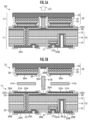
- FIG. 1A is a cross-sectional view schematically illustrating a cross section of the semiconductor light emitting device 10 according to a first embodiment of the present invention.
- FIG. 1B is a cross-sectional view illustrating separately a semiconductor light emitting element portion and a supporting substrate portion of the semiconductor light emitting device 10, corresponding to FIG. 1A.
- FIGS. 1A and 1B are cross-sectional views taken along the line A-A illustrated in FIGS. 2A and 3B .
- the semiconductor light emitting device 10 includes the supporting substrate 11 and the semiconductor light emitting element 31 bonded to the supporting substrate 11. More specifically, the supporting substrate 11 is formed of a first substrate semiconductor layer 13, a second substrate semiconductor layer 15, and an interlayer insulating film 14 provided between the first substrate semiconductor layer 13 and the second substrate semiconductor layer 15.
- a first mounting electrode 24A and a second mounting electrode 24B that are electrically connected to the semiconductor light emitting element 31 and drive the semiconductor light emitting element 31 are provided.
- a protective element 17 is provided on the second substrate semiconductor layer 15 of an SOI substrate 12.
- the protective element 17 is electrically connected to the semiconductor light emitting element 31 and functions as a protective circuit for the semiconductor light emitting element 31.
- the light emitting diode (hereinafter, also referred to as an LED element) 31 which is a semiconductor light emitting element includes an n-type semiconductor layer 33 as a second semiconductor layer, a p-type semiconductor layer 35 as a first semiconductor layer, and a semiconductor light emitting laminate 32 formed of a light emitting layer 34 provided between the n-type semiconductor layer 33 and the p-type semiconductor layer 35 (hereinafter, referred to as an LED semiconductor layer).
- the LED element 31 is bonded to the supporting substrate 11 with the p-type semiconductor layer 35 (first conductive type semiconductor layer) which is the growth outermost front surface layer as a lower surface, and the n-type semiconductor layer 33 (second conductive type semiconductor layer) is a front surface layer of the semiconductor light emitting device 10.
- the light emitted from the semiconductor light emitting element 31 is radiated from the n-type semiconductor layer 33 to the outside of the semiconductor light emitting device 10 (radiated light LO).
- the first conductive type is p-type and the second conductive type is n-type will be described, but the first conductive type may be n-type and the second conductive type may be p-type.
- FIG. 1B is a schematic cross-sectional view illustrating separately the supporting substrate 11 and the semiconductor light emitting element 31 for ease of description and understanding.
- the supporting substrate 11 and the semiconductor light emitting element 31 will be described in detail with reference to FIG. 1B .
- the supporting substrate 11 includes a substrate in which an interlayer insulating film is interposed between semiconductor layers, for example, the silicon on insulator (SOI) substrate 12.
- the first substrate semiconductor layer 13 and the second substrate semiconductor layer 15 are n-type Si (silicon) layers doped with, for example, P (phosphorus) or As (arsenic), and the interlayer insulating film 14 is an SiO 2 film.
- the first substrate semiconductor layer 13 and the second substrate semiconductor layer 15 will be referred to as an upper Si layer 13 and a lower Si layer 15, respectively.
- the supporting substrate 11 is not limited to a silicon on insulator (SOI) substrate.
- SOI silicon on insulator
- a substrate having a structure in which an interlayer insulating film is interposed between semiconductor layers such as Ge (germanium) is also referred to as a semiconductor on insulator (SOI) substrate.
- a first wiring electrode 22A and a second wiring electrode 22B are provided on an upper surface of the supporting substrate 11 (a surface on a bonding side with the LED element 31) (hereinafter, referred to as a wiring electrode 22 when not particularly distinguished).
- the first wiring electrode 22A is a p-wiring electrode connected to the first element electrode (p-electrode) of the semiconductor light emitting element 31
- the second wiring electrode 22B is an n-wiring electrode connected to the second element electrode (n-electrode) of the semiconductor light emitting element 31.
- the first wiring electrode (p-wiring electrode) 22A and the second wiring electrode (n-wiring electrode) 22B are protected by a protective film 28A which is an insulating film (for example, a SiO 2 film).
- the first wiring electrode 22A is provided via an insulating film 25 on the upper Si layer 13, and is electrically insulated from the upper Si layer 13.
- the second wiring electrode 22B is provided on the upper Si layer 13 and is in ohmic contact with the upper Si layer 13.
- first mounting electrode 24A and the second mounting electrode 24B (hereinafter, collectively referred to as a mounting electrode 24 when not particularly distinguished) are provided.
- the first mounting electrode 24A and the second mounting electrode 24B are connected to wiring on a circuit substrate such as a PCB substrate.
- the first mounting electrode 24A is an anode electrode and the second mounting electrode 24B is a cathode electrode.
- the anode electrode 24A and the cathode electrode 24B are protected by a protective film 28B which is an insulating film (for example, a SiO 2 film).
- the anode electrode 24A is connected to the first wiring electrode 22A via a metal via 23 that reaches from the back surface of the SOI substrate 12 (the back surface of the lower Si layer 15) to the upper surface (the front surface of the upper Si layer 13). Further, the first wiring electrode 22A, the metal via 23, and the anode electrode 24A are insulated from the SOI substrate 12 by the insulating film 25.
- a plurality of metal vias 23 are provided from the viewpoint of preventing conduction failure between the first wiring electrode 22A and the anode electrode 24A and improving heat dissipation of heat generated by the semiconductor light emitting element 31.
- the SOI substrate 12 is provided with a via (via hole) 26 that reaches from the back surface of the SOI substrate 12 to the front surface of the upper Si layer 13 or the inside thereof.
- the cathode electrode 24B is electrically connected to the upper Si layer 13 via the via 26.
- the cathode electrode 24B has a via electrode portion 24V that is formed on the insulating film 27 and reaches the upper Si layer 13 from the back surface of the lower Si layer 15. Further, the cathode electrode 24B is insulated from the lower Si layer 15.
- the via electrode portion 24V of the cathode electrode 24B is in ohmic contact with the upper Si layer 13 exposed from the via 26. Therefore, the cathode electrode 24B is electrically connected to the second wiring electrode 22B via the upper Si layer 13.
- the plurality of vias 26 including the via electrode portion 24V are provided from the viewpoint of preventing conduction failure between the second wiring electrode 22B and the upper Si layer 13A and improving heat dissipation of heat generated by the semiconductor light emitting element 31.
- the protective element 17 is provided on the lower Si layer 15 of the SOI substrate 12. More specifically, the lower Si layer 15 is formed with an impurity diffusion region 17D (p-Si region) in which impurities such as B (boron) or Al (aluminum) are diffused and the protective element 17 (broken part in the drawing) which is a Zener diode (ZD) is formed by pn bonding of the impurity diffusion region 17D and the lower Si layer 15 in contact with the impurity diffusion region 17D.
- impurity diffusion region 17D p-Si region
- ZD Zener diode
- the impurity diffusion region 17D (p-Si region), which is one end of the protective element 17, is connected to the cathode electrode 24B.
- the other end of the protective element 17 is connected to the lower Si layer 15 and electrically connected to the anode electrode 24A via the lower Si layer 15 (n-Si layer).
- a positive electrode (anode) and a negative electrode (cathode) of the protective element 17 are connected to the cathode electrode 24B and the anode electrode 24A of the semiconductor light emitting element 31, respectively, and are formed to be connected in parallel with the semiconductor light emitting element 31.
- the first wiring electrode 22A is made of, for example, Ni (nickel)/Au (gold), and the second wiring electrode 22B is made of, for example, Ti (titanium) or Ni/Au. Further, the anode electrode 24A and the cathode electrode 24B are made of, for example, Ni/Au. In these electrodes, Au is the front surface layer.
- the LED element 31 uses a so-called thin-film LED as the LED semiconductor layer (semiconductor light emitting laminate) 32. More specifically, the LED semiconductor layer 32 has a configuration in which a semiconductor laminate (thin-film LED) having an LED structure epitaxially grown on a growth substrate is removed from the growth substrate.
- the LED semiconductor layer 32 is not limited to a thin-film LED, and a semiconductor light emitting laminate in which a p-electrode and an n-electrode are provided on one surface side can be used.
- the LED semiconductor layer 32 includes the n-type semiconductor layer (second semiconductor layer) 33, the light emitting layer 34, and the p-type semiconductor layer (first semiconductor layer) 35.
- Each of the n-type semiconductor layer 33 and the p-type semiconductor layer 35 is composed of at least one semiconductor layer, and may have various semiconductor layers such as a barrier layer, a current diffusion layer, and a contact layer according to a design such as improved characteristics.
- the LED semiconductor layer 32 is, for example, a blue light emitting semiconductor layer formed of a GaN-based semiconductor layer, but is not limited thereto.
- the light emitting layer 34 has, for example, a single quantum well (SQW) or multiple quantum well (MQW) structure.
- the LED semiconductor layer 32 is provided with a p-electrode (first element electrode) 36A and an n-electrode (second element electrode) 36B.
- the p-electrode 36A is formed on the front surface of the p-type semiconductor layer 35 and is in ohmic contact with the p-type semiconductor layer 35.
- the LED semiconductor layer 32 is formed with vias 36V reaching the n-type semiconductor layer 33 from the front surface of the p-type semiconductor layer 35, and the n-electrode 36B is provided on the n-type semiconductor layer 33 exposed from the via 36V and is in ohmic contact with the n-type semiconductor layer 33.
- An element protective film 38 made of SiO 2 is provided on the side surface, the bottom surface (the surface on the bonding side with the supporting substrate 11), and the inner wall surface of the via 36V of the LED semiconductor layer 32.
- the element protective film 38 protects the side surface of the LED semiconductor layer 32 and the inner wall surfaces of the p-electrode 36A, the n-electrode 36B, and the via 36V.
- the p-electrode 36A is formed of an ITO/Ni/Pt/Ag layer in which ITO (indium tin oxide, Ni (nickel), Pt (platinum), and Ag (silver) reflective films of a translucent conductive film are formed on the p-type semiconductor layer 35 in this order.
- the p-electrode 36A is preferably provided with a reflective film, but may not be provided with a reflective film.
- the n-electrode 36B is formed of a (Ti or Ni)/Au layer in which Ti (titanium) or Ni (nickel), and Au (gold) are formed on the n-type semiconductor layer 33 in this order.
- the materials and structures of the p-electrode 36A and the n-electrode 36B are not limited to the above.
- the materials and structures can be appropriately selected in consideration of characteristics such as improvement of extraction efficiency by light reflection, ohmic characteristics, and element reliability (life).
- the supporting substrate 11 and the semiconductor light emitting element 31 are bonded by a bonding layer 41A and a bonding layer 41B to form the semiconductor light emitting device 10 illustrated in FIG. 1A .
- the first wiring electrode (p-wiring electrode) 22A of the supporting substrate 11 is bonded to the p-electrode 36A of the semiconductor light emitting element 31 by the bonding layer 41A.
- the second wiring electrode 22B of the supporting substrate 11 is bonded to the n-electrode 36B of the semiconductor light emitting element 31 by the bonding layer 41B.
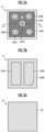
- FIG. 2A is a plan view schematically illustrating an upper surface of the supporting substrate 11, that is, a surface on a bonding side with the semiconductor light emitting element 31.
- FIG. 2B is a plan view schematically illustrating a back surface of the supporting substrate 11, that is, a surface of a circuit substrate such as a PCB substrate, on which the semiconductor light emitting device 10 is mounted.
- a plurality of circular second wiring electrodes 22B are disposed on the supporting substrate 11 (five in the case of the present embodiment).
- the plurality of second wiring electrodes 22B are insulated from the first wiring electrode (p-wiring electrode) 22A by the protective film 28A which is an insulating film.
- the plurality of second wiring electrodes 22B may be formed in a number, position, and size such that current diffusion is good and light emission becomes uniform.
- first wiring electrode 22A is disposed over the entire surface of the upper Si layer 13 of the SOI substrate 12, except for the regions of the plurality of second wiring electrodes 22B and the protective film 28A.
- the plurality of second wiring electrodes 22B are connected to the cathode electrode 24B on the back surface of the supporting substrate 11, and the first wiring electrode 22A is connected to the anode electrode 24A.
- FIG. 3A is a plan view schematically illustrating the upper surface of the semiconductor light emitting element 31, that is, the surface from which the radiated light LO is emitted, and the front surface of the n-type semiconductor layer 33.
- FIG. 3B is a plan view schematically illustrating a back surface (bonding surface with the supporting substrate 11) of the semiconductor light emitting element 31.
- the supporting substrate 11 has, so to speak, an electrode conversion function. Specifically, as illustrated in FIG. 3B , one p-electrode 36A and a plurality of n-electrodes 36B (in the case of the present embodiment, five) on the back surface (bonding surface with the supporting substrate 11) of the semiconductor light emitting element 31 are provided.
- At least one p-electrode 36A and one n-electrode 36B are provided, but it is preferable that a plurality of n-electrodes 36B are provided.
- the number, size, and disposition of the p-electrodes 36A and the n-electrodes 36B can be appropriately designed according to the current diffusion and the emission brightness.
- the first wiring electrode 22A and the second wiring electrode 22B corresponding to the number, size, and disposition of the p-electrodes 36A and the n-electrodes 36B of the semiconductor light emitting element 31 are provided on the upper surface (bonding surface with the semiconductor light emitting element 31) of the supporting substrate 11.
- a plurality of n-electrodes 36B are provided (n elements, where n is an integer of 2 or more).
- the plurality of n-electrodes 36B provided on the bottom surface of the semiconductor light emitting element 31 are disposed so as to be symmetrical positions.
- the plurality of n-electrodes 36B may be disposed at symmetrical positions with respect to a center point C of the semiconductor light emitting element 31 or the center line (for example, the symmetrical line A-A).
- the n-electrode 36B has a circular shape has been described as an example, but the present embodiment is not limited thereto.
- the n-electrode 36B may have a shape according to the shape and size of the semiconductor light emitting element 31, the number, size, and disposition of the n-electrode 36B, and the like. Further, the plurality of n-electrodes 36B may not have the same shape.
- the p-electrode 36A of the semiconductor light emitting element 31 is formed as an electrode over the entire surface of the p-type semiconductor layer 35, so-called full-surface electrode, except the region where the n-electrode 36B is formed (that is, the region of the n-electrode 36B and the region of the element protective film 38 protecting the edge of the n-electrode 36B).
- each anode electrode 24A and cathode electrode 24B are provided on the back surface of the supporting substrate 11 (that is, the surface of the circuit substrate on which the semiconductor light emitting device 10 is mounted), and the p-electrodes 36A and the n-electrodes 36B of the semiconductor light emitting element 31 are connected to each other.
- the anode electrode 24A and the cathode electrode 24B of the supporting substrate 11 can be integrated into each one, and it is possible to facilitate the wiring of the circuit substrate such as a PCB substrate.
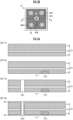
- FIGS. 4A to 4C are cross-sectional views schematically illustrating a manufacturing method of the supporting substrate 11.
- a method for manufacturing the supporting substrate 11 will be described in detail and specifically with reference to FIGS. 4A to 4C .
- the supporting substrate 11 was manufactured by the following steps-1 to 12 (ST-1 to ST-12).
- the SOI substrate 12 having the interlayer insulating film 14 formed of the upper Si layer 13 which is an n-Si layer doped with P or As, the lower Si layer 15, and a SiO 2 film was prepared.
- An impurity such as B or Al was diffused from the lower surface of the lower Si layer 15 by ion implantation, thermal diffusion, or the like to form a diffusion region 17D (p-Si region) of a p-impurity.
- the protective element 17 (broken part in the drawing) which is a Zener diode was formed in the lower Si layer 15.
- a SiO 2 film which is the substrate insulating film 25 was formed by plasma CVD using TEOS (tetraethoxysilane).
- TEOS tetraethoxysilane
- a copper (Cu) layer was formed on the front surface of the upper Si layer 13 and on the lower surface of the lower Si layer 15 by sputtering or electroless plating and electroplating.
- the inside of the via 23V was filled with Cu.
- a base metal layer 21A (the front surface of the upper Si layer 13) which is a Cu layer, a base metal layer 29 (the lower surface of the lower Si layer 15), and the metal vias 23 were formed.
- the via (through hole) 26 reaching from the lower surface of the lower Si layer 15 to the upper Si layer 13 was formed. More specifically, the via 26 was formed by etching while forming a SiO 2 film (insulating film 27) on the inner wall by a D-RIE (Deep RIE) process or a Bosch process.
- D-RIE Deep RIE
- the substrate insulating film 25 and the base metal layer (Cu layer) 29 were etched by wet etching or dry etching to form a hole portion 26R that exposes the impurity diffusion region 17D and the lower Si layer 15.
- Ni and Au were deposited on the lower surface of the lower Si layer 15 in this order by an electron beam (EB) method or sputtering to form a back surface electrode layer 24 which is a Ni/Au layer.
- EB electron beam
- the back surface electrode layer 24 thickly and embed the via 26 by the via electrode portion 24V. In this case, the heat dissipation by the via electrode portion 24V can be improved.
- the Ni/Au layer 22A was formed on the base metal layer (Cu layer) 21A on the upper Si layer 13.
- the base metal layer 21A and the Ni/Au layer 22A on the upper Si layer 13 and the base metal layer 29 and the back surface electrode layer 24 on the lower surface of the lower Si layer 15 were etched by wet etching or dry etching.
- the first wiring electrode 22A, the anode electrode 24A, and the cathode electrode 24B were patterned.
- step ST-10 Ti (titanium) or Ni, Au was deposited in this order on the upper Si layer 13 exposed in step ST-10 by an electron beam (EB) method or sputtering to form the second wiring electrode 22B which is (Ti or Ni)/Au layer.
- EB electron beam
- the substrate protective films 28A and 28B were formed by sputtering or plasma CVD using TEOS.
- the supporting substrate 11 was manufactured by the above steps ST-1 to ST-12.
- the heat transfer property (heat dissipation) in the vertical direction of the supporting substrate 11 is improved by the metal vias 23 and the via electrode portion 24V passing through the interlayer insulating film 14 that separates the first substrate semiconductor layer 13 and the second substrate semiconductor layer 15, in the vertical direction with respect to the film surface of the interlayer insulating film.
- the semiconductor light emitting device 10 was manufactured by bonding the supporting substrate 11 manufactured as described above to the semiconductor light emitting element 31 by the bonding layer 41A and the bonding layer 41B.
- the semiconductor light emitting device 10 of the first embodiment described above it is possible to provide a high-output semiconductor light emitting device that can obtain uniform light emission with high light emission efficiency. In addition, it is possible to provide a high-output semiconductor light emitting device that can obtain uniform light emission and is less likely to cause element destruction due to a protective element.
- FIG. 5A is a cross-sectional view schematically illustrating a cross section of the semiconductor light emitting device 50 according to a second embodiment of the present invention.
- FIG. 5B is a cross-sectional view illustrating separately a semiconductor light emitting element portion and a supporting substrate portion of the semiconductor light emitting device 50, corresponding to FIG. 5A .
- the semiconductor light emitting device 50 according to the second embodiment is the same as the semiconductor light emitting device 10 according to the first embodiment described above, in that a metal electrode layer is provided between the upper Si layer 13 and the insulating film 25.
- the metal electrode layer 55 is provided between the upper Si layer 13 and the first wiring electrode 22A, that is, on the upper Si layer 13.
- the metal electrode layer 55 is electrically connected to the second wiring electrode 22B (n-wiring electrode). Therefore, even in a case where the current diffusion is insufficient due to the resistivity of the upper Si layer 13 (n-Si layer), it is possible to improve current diffusion and to improve in-plane uniformity of light emission and light emission efficiency.
- the metal electrode layer 55 is preferably formed over the entire surface of the upper Si layer 13.
- FIG. 6 is a cross-sectional view schematically illustrating a method of forming the metal electrode layer 55.
- the metal electrode layer 55 is additionally executed as the following step ST-2A after step ST-2 described in the first embodiment.
- ST-3' and ST-4' are executed instead of ST-3 and ST-4 in the first embodiment.
- steps ST-5 to ST-12 described in the first embodiment are executed.
- the protective element 17 was formed in ST-2, Ti or Ni, and Au were deposited in this order by sputtering, an electron beam method, resistance heating deposition, plating, or the like, and the metal electrode layer 55 which is a (Ti or Ni)/Au layer was formed.
- a SiO 2 film which is the substrate insulating film 25 was formed by plasma CVD using TEOS (tetraethoxysilane).
- TEOS tetraethoxysilane
- the front surface of the upper Si layer 13, the front surface of the metal electrode layer 55, and the inner wall surface of the via 23V were coated with the insulating film 25.
- an insulating film formed on the metal electrode layer 55 is illustrated as the insulating film 25A (a part of the insulating film).
- the semiconductor light emitting device 50 of the second embodiment it is possible to provide a high-output semiconductor light emitting device that can obtain uniform light emission with higher light emission efficiency. Further, since the metal electrode layer 55 acts as a heat conductive layer (heat spreader) that guides the heat generated by the semiconductor light emitting element 31 to the vias 23 and 26, it is possible to provide a high-output semiconductor light emitting device. In addition, it is possible to provide a high-output semiconductor light emitting device that can obtain extremely uniform light emission and is less likely to cause element destruction due to a protective element.
- the semiconductor light emitting device of the present embodiment it is possible to provide a high-output semiconductor light emitting device that can obtain uniform light emission with high light emission efficiency. In addition, it is possible to provide a high-output semiconductor light emitting device that can obtain uniform light emission and is less likely to cause element destruction due to a protective element.
Landscapes
- Led Device Packages (AREA)
- Physics & Mathematics (AREA)
- Geometry (AREA)
Abstract
Description
- The present invention relates to a semiconductor light emitting device and a supporting substrate for semiconductor light emitting elements, and more particularly to a semiconductor light emitting device having a semiconductor light emitting element such as a light emitting diode (LED) and a supporting substrate for the semiconductor light emitting elements.
- In recent years, in order to increase the output and control a light distribution, semiconductor light emitting elements such as a light emitting diode (LED) are disposed and used in a plurality of devices.
- For example, in an automobile headlight, a variable light-distribution head lamp (ADB: Adaptive Driving Beam) that controls a light distribution according to a driving environment is known. In addition, LED packages for high-output lighting and LED packages for information and communication equipment in which LEDs are disposed at a high density, or the like are known.
- However, there is a further demand for high-output semiconductor light emitting elements that can obtain uniform light emission with high light emission efficiency. Further, there is a demand for a semiconductor light emitting device which has an additional function such as a protective element while preventing a deterioration in the performance of the light emitting element and is less likely to cause element destruction.
- For example,
Patent Literature 1 discloses a semiconductor light emitting device including a light emitting element having a protective element formed on a back surface of the light emitting element mounted on a resin carrier. Further,Patent Literature 2 discloses a semiconductor light emitting device in which a protective element is provided on a mounting substrate of a light emitting element.Patent Literature 3 discloses a semiconductor light emitting device in which a protective element is provided in a semiconductor substrate. -
- Patent Literature 1:
Japanese Patent No. 6571805 - Patent Literature 2: International Publication No.
WO2013/187318 - Patent Literature 3: US Patent
US 2013/0020598 A1 - The present invention has been made in view of the above points, and an object of the present invention is to provide a high-output semiconductor light emitting device that can obtain uniform light emission with high light emission efficiency. Another object of the present invention is to provide a semiconductor light emitting device that can obtain uniform light emission with high light emission efficiency and is less likely to cause element destruction due to a protective element.
- Further, the present invention provides a supporting substrate used for a high-output semiconductor light emitting element that can obtain uniform light emission with high light emission efficiency and is less likely to cause element destruction due to a protective element.
- The semiconductor light emitting device according to an embodiment of the present invention includes
- a semiconductor light emitting laminate in which a first conductive type first semiconductor layer, a light emitting layer, and a second conductive type second semiconductor layer are laminated, and that is provided with at least one first element electrode connected to the first semiconductor layer and at least one second element electrode connected to the second semiconductor layer on a surface on the first semiconductor layer side, and
- an SOI substrate that is formed of an upper semiconductor layer, a lower semiconductor layer, and an interlayer insulating film provided between the upper semiconductor layer and the lower semiconductor layer, in which
- the SOI substrate includes
- at least one first wiring electrode that is provided on the upper semiconductor layer through an insulating film and corresponds to the at least one first element electrode of the semiconductor light emitting element, and at least one second wiring electrode that is provided on the upper semiconductor layer by being connected to the upper semiconductor layer and corresponds to the at least one second element electrode of the semiconductor light emitting laminate,
- a first mounting electrode that is provided on the lower semiconductor layer and connected to the at least one first wiring electrode by a first via electrode passing through the SOI substrate, and
- a second mounting electrode that is provided on the lower semiconductor layer through the insulating film and connected to the upper semiconductor layer by a second via electrode passing through the lower semiconductor layer and the interlayer insulating film to reach the upper semiconductor layer, and
- the at least one first element electrode and the at least one second element electrode of the semiconductor light emitting laminate are respectively bonded to the at least one first wiring electrode and the at least one second wiring electrode of the SOI substrate.
- A supporting substrate according to another embodiment of the present invention is
- a supporting substrate for mounting a semiconductor light emitting element that includes first and second semiconductor layers each having first and second conductive types, and a light emitting layer provided between the first and second semiconductor layers, and that is provided with at least one first electrode connected to the first semiconductor layer and at least one second electrode connected to the second semiconductor layer on one surface side, the supporting substrate including
- an SOI substrate that is formed of an upper semiconductor layer, a lower semiconductor layer, and an interlayer insulating film provided between the upper semiconductor layer and the lower semiconductor layer, in which
- the SOI substrate includes
- at least one first wiring electrode that is provided on the upper semiconductor layer through an insulating film and corresponds to the at least one first electrode of the semiconductor light emitting element, and at least one second wiring electrode that is provided on the upper semiconductor layer by being connected to the upper semiconductor layer and corresponds to the at least one second electrode of the semiconductor light emitting laminate,
- a first mounting electrode that is provided on the lower semiconductor layer and connected to the at least one first wiring electrode by a first via electrode passing through the SOI substrate, and
- a second mounting electrode that is provided on the lower semiconductor layer through the insulating film and connected to the upper semiconductor layer by a second via electrode passing through the lower semiconductor layer and the interlayer insulating film to reach the upper semiconductor layer.
-
-
FIG. 1A is a cross-sectional view schematically illustrating a cross section of a semiconductorlight emitting device 10 according to a first embodiment of the present invention. -
FIG. 1B is a cross-sectional view illustrating separately a semiconductor light emitting element portion and a supporting substrate portion of the semiconductorlight emitting device 10. -
FIG. 1C is a circuit view illustrating a connection between aprotective element 17 and a semiconductorlight emitting element 31. -
FIG. 2A is a plan view schematically illustrating an upper surface of a supportingsubstrate 11, that is, a surface on a bonding side with the semiconductorlight emitting element 31. -
FIG. 2B is a plan view schematically illustrating a back surface of the supportingsubstrate 11, that is, a surface of a circuit substrate such as a PCB substrate, on which the semiconductorlight emitting device 10 is mounted. -
FIG. 3A is a plan view schematically illustrating an upper surface of the semiconductorlight emitting element 31. -
FIG. 3B is a plan view schematically illustrating a back surface (bonding surface with the supporting substrate 11) of the semiconductorlight emitting element 31. -
FIG. 4A is a cross-sectional view schematically illustrating a manufacturing method of the supportingsubstrate 11. -
FIG. 4B is a cross-sectional view schematically illustrating a manufacturing method of the supportingsubstrate 11. -
FIG. 4C is a cross-sectional view schematically illustrating a manufacturing method of the supportingsubstrate 11. -
FIG. 5A is a cross-sectional view schematically illustrating a cross section of a semiconductorlight emitting device 50 according to a second embodiment of the present invention. -
FIG. 5B is a cross-sectional view illustrating separately the semiconductorlight emitting element 31 and the supportingsubstrate 11 of the semiconductorlight emitting device 50 according to the second embodiment. -
FIG. 6 is a cross-sectional view schematically illustrating a method of forming ametal electrode layer 55 in the second embodiment. - Hereinafter, preferred embodiments of the present invention will be described, but these embodiments may be appropriately modified and combined. In addition, in the following description and the accompanying drawings, substantially the same or equivalent parts will be described with the same reference numerals.
-
FIG. 1A is a cross-sectional view schematically illustrating a cross section of the semiconductorlight emitting device 10 according to a first embodiment of the present invention.FIG. 1B is a cross-sectional view illustrating separately a semiconductor light emitting element portion and a supporting substrate portion of the semiconductorlight emitting device 10, corresponding toFIG. 1A. FIGS. 1A and 1B are cross-sectional views taken along the line A-A illustrated inFIGS. 2A and3B . - The semiconductor
light emitting device 10 includes the supportingsubstrate 11 and the semiconductorlight emitting element 31 bonded to the supportingsubstrate 11. More specifically, the supportingsubstrate 11 is formed of a firstsubstrate semiconductor layer 13, a secondsubstrate semiconductor layer 15, and aninterlayer insulating film 14 provided between the firstsubstrate semiconductor layer 13 and the secondsubstrate semiconductor layer 15. - Further, on the back surface of the supporting
substrate 11, a first mountingelectrode 24A and asecond mounting electrode 24B that are electrically connected to the semiconductorlight emitting element 31 and drive the semiconductorlight emitting element 31 are provided. - In addition, a
protective element 17 is provided on the secondsubstrate semiconductor layer 15 of anSOI substrate 12. Theprotective element 17 is electrically connected to the semiconductorlight emitting element 31 and functions as a protective circuit for the semiconductorlight emitting element 31. - The light emitting diode (hereinafter, also referred to as an LED element) 31 which is a semiconductor light emitting element includes an n-
type semiconductor layer 33 as a second semiconductor layer, a p-type semiconductor layer 35 as a first semiconductor layer, and a semiconductorlight emitting laminate 32 formed of alight emitting layer 34 provided between the n-type semiconductor layer 33 and the p-type semiconductor layer 35 (hereinafter, referred to as an LED semiconductor layer). - In the present embodiment, the
LED element 31 is bonded to the supportingsubstrate 11 with the p-type semiconductor layer 35 (first conductive type semiconductor layer) which is the growth outermost front surface layer as a lower surface, and the n-type semiconductor layer 33 (second conductive type semiconductor layer) is a front surface layer of the semiconductorlight emitting device 10. The light emitted from the semiconductorlight emitting element 31 is radiated from the n-type semiconductor layer 33 to the outside of the semiconductor light emitting device 10 (radiated light LO). - In the present embodiment, a case where the first conductive type is p-type and the second conductive type is n-type will be described, but the first conductive type may be n-type and the second conductive type may be p-type.
-
FIG. 1B is a schematic cross-sectional view illustrating separately the supportingsubstrate 11 and the semiconductorlight emitting element 31 for ease of description and understanding. Hereinafter, the supportingsubstrate 11 and the semiconductorlight emitting element 31 will be described in detail with reference toFIG. 1B . - The supporting
substrate 11 includes a substrate in which an interlayer insulating film is interposed between semiconductor layers, for example, the silicon on insulator (SOI)substrate 12. The firstsubstrate semiconductor layer 13 and the secondsubstrate semiconductor layer 15 are n-type Si (silicon) layers doped with, for example, P (phosphorus) or As (arsenic), and theinterlayer insulating film 14 is an SiO2 film. Hereinafter, the firstsubstrate semiconductor layer 13 and the secondsubstrate semiconductor layer 15 will be referred to as anupper Si layer 13 and alower Si layer 15, respectively. - The supporting
substrate 11 is not limited to a silicon on insulator (SOI) substrate. In the present specification, a substrate having a structure in which an interlayer insulating film is interposed between semiconductor layers such as Ge (germanium) is also referred to as a semiconductor on insulator (SOI) substrate. - A
first wiring electrode 22A and asecond wiring electrode 22B are provided on an upper surface of the supporting substrate 11 (a surface on a bonding side with the LED element 31) (hereinafter, referred to as a wiring electrode 22 when not particularly distinguished). - In the present embodiment, the
first wiring electrode 22A is a p-wiring electrode connected to the first element electrode (p-electrode) of the semiconductorlight emitting element 31, and thesecond wiring electrode 22B is an n-wiring electrode connected to the second element electrode (n-electrode) of the semiconductorlight emitting element 31. - The first wiring electrode (p-wiring electrode) 22A and the second wiring electrode (n-wiring electrode) 22B are protected by a
protective film 28A which is an insulating film (for example, a SiO2 film). Thefirst wiring electrode 22A is provided via an insulatingfilm 25 on theupper Si layer 13, and is electrically insulated from theupper Si layer 13. Thesecond wiring electrode 22B is provided on theupper Si layer 13 and is in ohmic contact with theupper Si layer 13. - Further, on the back surface of the supporting
substrate 11, the first mountingelectrode 24A and thesecond mounting electrode 24B (hereinafter, collectively referred to as a mountingelectrode 24 when not particularly distinguished) are provided. Thefirst mounting electrode 24A and thesecond mounting electrode 24B are connected to wiring on a circuit substrate such as a PCB substrate. - In the present embodiment, the first mounting
electrode 24A is an anode electrode and thesecond mounting electrode 24B is a cathode electrode. Theanode electrode 24A and thecathode electrode 24B are protected by aprotective film 28B which is an insulating film (for example, a SiO2 film). - The
anode electrode 24A is connected to thefirst wiring electrode 22A via a metal via 23 that reaches from the back surface of the SOI substrate 12 (the back surface of the lower Si layer 15) to the upper surface (the front surface of the upper Si layer 13). Further, thefirst wiring electrode 22A, the metal via 23, and theanode electrode 24A are insulated from theSOI substrate 12 by the insulatingfilm 25. - It is desirable that a plurality of
metal vias 23 are provided from the viewpoint of preventing conduction failure between thefirst wiring electrode 22A and theanode electrode 24A and improving heat dissipation of heat generated by the semiconductorlight emitting element 31. - The
SOI substrate 12 is provided with a via (via hole) 26 that reaches from the back surface of theSOI substrate 12 to the front surface of theupper Si layer 13 or the inside thereof. Thecathode electrode 24B is electrically connected to theupper Si layer 13 via the via 26. - More specifically, an insulating
film 27 is provided on the inner wall of the via 26. Thecathode electrode 24B has a via electrode portion 24V that is formed on the insulatingfilm 27 and reaches theupper Si layer 13 from the back surface of thelower Si layer 15. Further, thecathode electrode 24B is insulated from thelower Si layer 15. - The via electrode portion 24V of the
cathode electrode 24B is in ohmic contact with theupper Si layer 13 exposed from the via 26. Therefore, thecathode electrode 24B is electrically connected to thesecond wiring electrode 22B via theupper Si layer 13. - It is desirable that the plurality of
vias 26 including the via electrode portion 24V are provided from the viewpoint of preventing conduction failure between thesecond wiring electrode 22B and the upper Si layer 13A and improving heat dissipation of heat generated by the semiconductorlight emitting element 31. - Further, the
protective element 17 is provided on thelower Si layer 15 of theSOI substrate 12. More specifically, thelower Si layer 15 is formed with animpurity diffusion region 17D (p-Si region) in which impurities such as B (boron) or Al (aluminum) are diffused and the protective element 17 (broken part in the drawing) which is a Zener diode (ZD) is formed by pn bonding of theimpurity diffusion region 17D and thelower Si layer 15 in contact with theimpurity diffusion region 17D. - The
impurity diffusion region 17D (p-Si region), which is one end of theprotective element 17, is connected to thecathode electrode 24B. The other end of theprotective element 17 is connected to thelower Si layer 15 and electrically connected to theanode electrode 24A via the lower Si layer 15 (n-Si layer). - More specifically, as illustrated in
FIG. 1C , a positive electrode (anode) and a negative electrode (cathode) of theprotective element 17 are connected to thecathode electrode 24B and theanode electrode 24A of the semiconductorlight emitting element 31, respectively, and are formed to be connected in parallel with the semiconductorlight emitting element 31. - The
first wiring electrode 22A is made of, for example, Ni (nickel)/Au (gold), and thesecond wiring electrode 22B is made of, for example, Ti (titanium) or Ni/Au. Further, theanode electrode 24A and thecathode electrode 24B are made of, for example, Ni/Au. In these electrodes, Au is the front surface layer. - In the first embodiment, the
LED element 31 uses a so-called thin-film LED as the LED semiconductor layer (semiconductor light emitting laminate) 32. More specifically, theLED semiconductor layer 32 has a configuration in which a semiconductor laminate (thin-film LED) having an LED structure epitaxially grown on a growth substrate is removed from the growth substrate. - The
LED semiconductor layer 32 is not limited to a thin-film LED, and a semiconductor light emitting laminate in which a p-electrode and an n-electrode are provided on one surface side can be used. - The
LED semiconductor layer 32 includes the n-type semiconductor layer (second semiconductor layer) 33, thelight emitting layer 34, and the p-type semiconductor layer (first semiconductor layer) 35. Each of the n-type semiconductor layer 33 and the p-type semiconductor layer 35 is composed of at least one semiconductor layer, and may have various semiconductor layers such as a barrier layer, a current diffusion layer, and a contact layer according to a design such as improved characteristics. - The
LED semiconductor layer 32 is, for example, a blue light emitting semiconductor layer formed of a GaN-based semiconductor layer, but is not limited thereto. Thelight emitting layer 34 has, for example, a single quantum well (SQW) or multiple quantum well (MQW) structure. - The
LED semiconductor layer 32 is provided with a p-electrode (first element electrode) 36A and an n-electrode (second element electrode) 36B. The p-electrode 36A is formed on the front surface of the p-type semiconductor layer 35 and is in ohmic contact with the p-type semiconductor layer 35. - The
LED semiconductor layer 32 is formed withvias 36V reaching the n-type semiconductor layer 33 from the front surface of the p-type semiconductor layer 35, and the n-electrode 36B is provided on the n-type semiconductor layer 33 exposed from the via 36V and is in ohmic contact with the n-type semiconductor layer 33. - An element
protective film 38 made of SiO2 is provided on the side surface, the bottom surface (the surface on the bonding side with the supporting substrate 11), and the inner wall surface of thevia 36V of theLED semiconductor layer 32. The elementprotective film 38 protects the side surface of theLED semiconductor layer 32 and the inner wall surfaces of the p-electrode 36A, the n-electrode 36B, and thevia 36V. - The p-
electrode 36A is formed of an ITO/Ni/Pt/Ag layer in which ITO (indium tin oxide, Ni (nickel), Pt (platinum), and Ag (silver) reflective films of a translucent conductive film are formed on the p-type semiconductor layer 35 in this order. The p-electrode 36A is preferably provided with a reflective film, but may not be provided with a reflective film. - The n-
electrode 36B is formed of a (Ti or Ni)/Au layer in which Ti (titanium) or Ni (nickel), and Au (gold) are formed on the n-type semiconductor layer 33 in this order. - The materials and structures of the p-
electrode 36A and the n-electrode 36B are not limited to the above. The materials and structures can be appropriately selected in consideration of characteristics such as improvement of extraction efficiency by light reflection, ohmic characteristics, and element reliability (life). - The supporting
substrate 11 and the semiconductorlight emitting element 31 are bonded by abonding layer 41A and abonding layer 41B to form the semiconductorlight emitting device 10 illustrated inFIG. 1A . - More specifically, the first wiring electrode (p-wiring electrode) 22A of the supporting
substrate 11 is bonded to the p-electrode 36A of the semiconductorlight emitting element 31 by thebonding layer 41A. Thesecond wiring electrode 22B of the supportingsubstrate 11 is bonded to the n-electrode 36B of the semiconductorlight emitting element 31 by thebonding layer 41B. -
FIG. 2A is a plan view schematically illustrating an upper surface of the supportingsubstrate 11, that is, a surface on a bonding side with the semiconductorlight emitting element 31.FIG. 2B is a plan view schematically illustrating a back surface of the supportingsubstrate 11, that is, a surface of a circuit substrate such as a PCB substrate, on which the semiconductorlight emitting device 10 is mounted. - As illustrated in
FIG. 2A , a plurality of circularsecond wiring electrodes 22B (n-wiring electrodes) are disposed on the supporting substrate 11 (five in the case of the present embodiment). The plurality ofsecond wiring electrodes 22B are insulated from the first wiring electrode (p-wiring electrode) 22A by theprotective film 28A which is an insulating film. - The plurality of
second wiring electrodes 22B may be formed in a number, position, and size such that current diffusion is good and light emission becomes uniform. - In addition, the
first wiring electrode 22A is disposed over the entire surface of theupper Si layer 13 of theSOI substrate 12, except for the regions of the plurality ofsecond wiring electrodes 22B and theprotective film 28A. - As illustrated in
FIGS. 1B and2B , the plurality ofsecond wiring electrodes 22B are connected to thecathode electrode 24B on the back surface of the supportingsubstrate 11, and thefirst wiring electrode 22A is connected to theanode electrode 24A. -
FIG. 3A is a plan view schematically illustrating the upper surface of the semiconductorlight emitting element 31, that is, the surface from which the radiated light LO is emitted, and the front surface of the n-type semiconductor layer 33. Further,FIG. 3B is a plan view schematically illustrating a back surface (bonding surface with the supporting substrate 11) of the semiconductorlight emitting element 31. - The supporting
substrate 11 has, so to speak, an electrode conversion function. Specifically, as illustrated inFIG. 3B , one p-electrode 36A and a plurality of n-electrodes 36B (in the case of the present embodiment, five) on the back surface (bonding surface with the supporting substrate 11) of the semiconductorlight emitting element 31 are provided. - It is sufficient that at least one p-
electrode 36A and one n-electrode 36B are provided, but it is preferable that a plurality of n-electrodes 36B are provided. The number, size, and disposition of the p-electrodes 36A and the n-electrodes 36B can be appropriately designed according to the current diffusion and the emission brightness. - On the other hand, as illustrated in
FIG. 2A , thefirst wiring electrode 22A and thesecond wiring electrode 22B corresponding to the number, size, and disposition of the p-electrodes 36A and the n-electrodes 36B of the semiconductorlight emitting element 31 are provided on the upper surface (bonding surface with the semiconductor light emitting element 31) of the supportingsubstrate 11. - It is preferable that a plurality of n-
electrodes 36B are provided (n elements, where n is an integer of 2 or more). In this case, it is preferable that the plurality of n-electrodes 36B provided on the bottom surface of the semiconductorlight emitting element 31 are disposed so as to be symmetrical positions. For example, as illustrated inFIG. 3B , it is preferable that the plurality of n-electrodes 36B may be disposed at symmetrical positions with respect to a center point C of the semiconductorlight emitting element 31 or the center line (for example, the symmetrical line A-A). - Further, in the present embodiment, the case where the n-
electrode 36B has a circular shape has been described as an example, but the present embodiment is not limited thereto. The n-electrode 36B may have a shape according to the shape and size of the semiconductorlight emitting element 31, the number, size, and disposition of the n-electrode 36B, and the like. Further, the plurality of n-electrodes 36B may not have the same shape. - Further, as illustrated in
FIG. 3B , it is preferable that the p-electrode 36A of the semiconductorlight emitting element 31 is formed as an electrode over the entire surface of the p-type semiconductor layer 35, so-called full-surface electrode, except the region where the n-electrode 36B is formed (that is, the region of the n-electrode 36B and the region of the elementprotective film 38 protecting the edge of the n-electrode 36B). - As illustrated in
FIG. 2B , eachanode electrode 24A andcathode electrode 24B are provided on the back surface of the supporting substrate 11 (that is, the surface of the circuit substrate on which the semiconductorlight emitting device 10 is mounted), and the p-electrodes 36A and the n-electrodes 36B of the semiconductorlight emitting element 31 are connected to each other. - That is, even when a plurality of p-
electrodes 36A and/or n-electrodes 36B are provided in the semiconductorlight emitting element 31 in order to improve element characteristics such as current diffusion, theanode electrode 24A and thecathode electrode 24B of the supportingsubstrate 11 can be integrated into each one, and it is possible to facilitate the wiring of the circuit substrate such as a PCB substrate. - Hereinafter,
FIGS. 4A to 4C are cross-sectional views schematically illustrating a manufacturing method of the supportingsubstrate 11. A method for manufacturing the supportingsubstrate 11 will be described in detail and specifically with reference toFIGS. 4A to 4C . The supportingsubstrate 11 was manufactured by the following steps-1 to 12 (ST-1 to ST-12). - The
SOI substrate 12 having the interlayer insulatingfilm 14 formed of theupper Si layer 13 which is an n-Si layer doped with P or As, thelower Si layer 15, and a SiO2 film was prepared. - An impurity such as B or Al was diffused from the lower surface of the
lower Si layer 15 by ion implantation, thermal diffusion, or the like to form adiffusion region 17D (p-Si region) of a p-impurity. As a result, the protective element 17 (broken part in the drawing) which is a Zener diode was formed in thelower Si layer 15. - A Via (through hole) 23V reaching from the lower surface of the
lower Si layer 15 to the front surface of theupper Si layer 13 was formed. - A SiO2 film which is the
substrate insulating film 25 was formed by plasma CVD using TEOS (tetraethoxysilane). The front surface of theupper Si layer 13, the lower surface of thelower Si layer 15, and the inner wall surface of the via 23V were coated with the insulatingfilm 25. - A copper (Cu) layer was formed on the front surface of the
upper Si layer 13 and on the lower surface of thelower Si layer 15 by sputtering or electroless plating and electroplating. In addition, the inside of the via 23V was filled with Cu. - As a result, a
base metal layer 21A (the front surface of the upper Si layer 13) which is a Cu layer, a base metal layer 29 (the lower surface of the lower Si layer 15), and themetal vias 23 were formed. - The via (through hole) 26 reaching from the lower surface of the
lower Si layer 15 to theupper Si layer 13 was formed. More specifically, the via 26 was formed by etching while forming a SiO2 film (insulating film 27) on the inner wall by a D-RIE (Deep RIE) process or a Bosch process. - The
substrate insulating film 25 and the base metal layer (Cu layer) 29 were etched by wet etching or dry etching to form ahole portion 26R that exposes theimpurity diffusion region 17D and thelower Si layer 15. - Ni and Au were deposited on the lower surface of the
lower Si layer 15 in this order by an electron beam (EB) method or sputtering to form a backsurface electrode layer 24 which is a Ni/Au layer. - As a result, an ohmic contact between the
diffusion region 17D and thelower Si layer 15 that serve as electrodes of the protective element (Zener diode) 17 was formed. In addition, the via electrode portion 24V of thecathode electrode 24B, which is an ohmic contact electrode with theupper Si layer 13, was formed. - It is also possible to form the back
surface electrode layer 24 thickly and embed the via 26 by the via electrode portion 24V. In this case, the heat dissipation by the via electrode portion 24V can be improved. - The Ni/
Au layer 22A was formed on the base metal layer (Cu layer) 21A on theupper Si layer 13. - The
base metal layer 21A and the Ni/Au layer 22A on theupper Si layer 13 and thebase metal layer 29 and the backsurface electrode layer 24 on the lower surface of thelower Si layer 15 were etched by wet etching or dry etching. - As a result, the
first wiring electrode 22A, theanode electrode 24A, and thecathode electrode 24B were patterned. - Ti (titanium) or Ni, Au was deposited in this order on the
upper Si layer 13 exposed in step ST-10 by an electron beam (EB) method or sputtering to form thesecond wiring electrode 22B which is (Ti or Ni)/Au layer. - The substrate
protective films - The supporting
substrate 11 was manufactured by the above steps ST-1 to ST-12. - In particular, the heat transfer property (heat dissipation) in the vertical direction of the supporting
substrate 11 is improved by themetal vias 23 and the via electrode portion 24V passing through theinterlayer insulating film 14 that separates the firstsubstrate semiconductor layer 13 and the secondsubstrate semiconductor layer 15, in the vertical direction with respect to the film surface of the interlayer insulating film. - As described above, the semiconductor
light emitting device 10 was manufactured by bonding the supportingsubstrate 11 manufactured as described above to the semiconductorlight emitting element 31 by thebonding layer 41A and thebonding layer 41B. - According to the semiconductor
light emitting device 10 of the first embodiment described above, it is possible to provide a high-output semiconductor light emitting device that can obtain uniform light emission with high light emission efficiency. In addition, it is possible to provide a high-output semiconductor light emitting device that can obtain uniform light emission and is less likely to cause element destruction due to a protective element. - Further, it is possible to provide a high-output semiconductor light emitting device by improving heat dissipation by means of the
metal vias 23 penetrating theinterlayer insulating film 14 and the via electrode portion 24V. - In addition, it is possible to provide a high-output semiconductor light emitting device that facilitates wiring of a circuit substrate or the like on which a semiconductor light emitting device is mounted.
-
FIG. 5A is a cross-sectional view schematically illustrating a cross section of the semiconductorlight emitting device 50 according to a second embodiment of the present invention.FIG. 5B is a cross-sectional view illustrating separately a semiconductor light emitting element portion and a supporting substrate portion of the semiconductorlight emitting device 50, corresponding toFIG. 5A . - The semiconductor
light emitting device 50 according to the second embodiment is the same as the semiconductorlight emitting device 10 according to the first embodiment described above, in that a metal electrode layer is provided between theupper Si layer 13 and the insulatingfilm 25. - More specifically, as illustrated in
FIGS. 5A and 5B , when the insulating film between theupper Si layer 13 and thefirst wiring electrode 22A provided on theupper Si layer 13 side is aninsulating film 25A, themetal electrode layer 55 is provided between theupper Si layer 13 and thefirst wiring electrode 22A, that is, on theupper Si layer 13. - The
metal electrode layer 55 is electrically connected to thesecond wiring electrode 22B (n-wiring electrode). Therefore, even in a case where the current diffusion is insufficient due to the resistivity of the upper Si layer 13 (n-Si layer), it is possible to improve current diffusion and to improve in-plane uniformity of light emission and light emission efficiency. - The
metal electrode layer 55 is preferably formed over the entire surface of theupper Si layer 13. -
FIG. 6 is a cross-sectional view schematically illustrating a method of forming themetal electrode layer 55. Themetal electrode layer 55 is additionally executed as the following step ST-2A after step ST-2 described in the first embodiment. - In addition, ST-3' and ST-4' are executed instead of ST-3 and ST-4 in the first embodiment. After step ST-5, steps ST-5 to ST-12 described in the first embodiment are executed.
- After the
protective element 17 was formed in ST-2, Ti or Ni, and Au were deposited in this order by sputtering, an electron beam method, resistance heating deposition, plating, or the like, and themetal electrode layer 55 which is a (Ti or Ni)/Au layer was formed. - The via (through hole) 23V reaching the front surface of the
metal electrode layer 55 from the lower surface of thelower Si layer 15 was formed. - A SiO2 film which is the
substrate insulating film 25 was formed by plasma CVD using TEOS (tetraethoxysilane). The front surface of theupper Si layer 13, the front surface of themetal electrode layer 55, and the inner wall surface of the via 23V were coated with the insulatingfilm 25. Here, an insulating film formed on themetal electrode layer 55 is illustrated as the insulatingfilm 25A (a part of the insulating film). - As described above, according to the semiconductor
light emitting device 50 of the second embodiment, it is possible to provide a high-output semiconductor light emitting device that can obtain uniform light emission with higher light emission efficiency. Further, since themetal electrode layer 55 acts as a heat conductive layer (heat spreader) that guides the heat generated by the semiconductorlight emitting element 31 to thevias - As described in detail above, according to the semiconductor light emitting device of the present embodiment, it is possible to provide a high-output semiconductor light emitting device that can obtain uniform light emission with high light emission efficiency. In addition, it is possible to provide a high-output semiconductor light emitting device that can obtain uniform light emission and is less likely to cause element destruction due to a protective element.
- In addition, it is possible to provide a high-output semiconductor light emitting device that facilitates wiring of a circuit substrate or the like on which a semiconductor light emitting device is mounted.
- Furthermore, it is possible to provide a supporting substrate used for a high-output semiconductor light emitting element that can obtain uniform light emission with high light emission efficiency and is less likely to cause element destruction due to a protective element.
-
- 10, 50: semiconductor light emitting device
- 11: supporting substrate
- 12: SOI substrate
- 13: first substrate semiconductor layer
- 14: interlayer insulating film
- 15: second substrate semiconductor layer
- 17: protective element
- 17D: impurity diffusion region
- 22A: first wiring electrode
- 22B: second wiring electrode
- 23: metal via
- 24A: anode electrode
- 24B: cathode electrode
- 25, 25A: insulating film
- 26: via (through hole)
- 28A, 28B, 38A, 38B: protective film
- 31: semiconductor light emitting element
- 32: semiconductor light emitting laminate
- 33: n-type semiconductor layer
- 34: light emitting layer
- 35: p-type semiconductor layer
- 36A: p-electrode
- 36B: n-electrode
- 55: metal electrode layer
Claims (11)
- A semiconductor light emitting device comprising:a semiconductor light emitting laminate in which a first conductive type first semiconductor layer, a light emitting layer, and a second conductive type second semiconductor layer are laminated, and that is provided with at least one first element electrode connected to the first semiconductor layer and at least one second element electrode connected to the second semiconductor layer on a surface on the first semiconductor layer side; andan SOI substrate that is formed of an upper semiconductor layer, a lower semiconductor layer, and an interlayer insulating film provided between the upper semiconductor layer and the lower semiconductor layer, whereinthe SOI substrate includesat least one first wiring electrode that is provided on the upper semiconductor layer through an insulating film and corresponds to the at least one first element electrode of the semiconductor light emitting element, and at least one second wiring electrode that is provided on the upper semiconductor layer by being connected to the upper semiconductor layer and corresponds to the at least one second element electrode of the semiconductor light emitting laminate,a first mounting electrode that is provided on the lower semiconductor layer and connected to the at least one first wiring electrode by a first via electrode passing through the SOI substrate, anda second mounting electrode that is provided on the lower semiconductor layer through the insulating film and connected to the upper semiconductor layer by a second via electrode passing through the lower semiconductor layer and the interlayer insulating film to reach the upper semiconductor layer, andthe at least one first element electrode and the at least one second element electrode of the semiconductor light emitting laminate are respectively bonded to the at least one first wiring electrode and the at least one second wiring electrode of the SOI substrate.
- The semiconductor light emitting device according to claim 1, wherein
the upper semiconductor layer and the lower semiconductor layer are n-Si layers, and the lower semiconductor layer is connected to the first mounting electrode and includes an impurity diffusion region that is provided on a front surface of the lower semiconductor layer, and is connected to the second mounting electrode to form a pn bonding in the lower semiconductor layer. - The semiconductor light emitting device according to claim 1 or 2, wherein
the first conductive type and the second conductive type are p-type and n-type, respectively, and the at least one second element electrode is provided on the second semiconductor layer exposed from a via reaching the second semiconductor layer from a front surface of the first semiconductor layer. - The semiconductor light emitting device according to any one of claims 1 to 3, wherein
the first conductive type and the second conductive type are p-type and n-type, respectively, and the at least one first element electrode includes a translucent conductive film and a reflective film. - The semiconductor light emitting device according to any one of claims 1 to 4, wherein
the semiconductor light emitting laminate includes a plurality of the second element electrodes, and the plurality of second element electrodes are disposed at symmetrical positions on the surface of the first semiconductor layer side. - The semiconductor light emitting device according to any one of claims 1 to 5, wherein
the first element electrode is formed as a full-surface electrode over an entire surface of the first semiconductor layer except for a region of the at least one second wiring electrode. - The semiconductor light emitting device according to any one of claims 1 to 6, further comprising:
a metal electrode layer that is provided on the upper semiconductor layer and connected to the at least one second wiring electrode. - The semiconductor light emitting device according to claim 7, wherein
the metal electrode layer is formed over an entire surface of the upper semiconductor layer. - A supporting substrate for mounting a semiconductor light emitting element that includes first and second semiconductor layers each having first and second conductive types, and a light emitting layer provided between the first and second semiconductor layers, and that is provided with at least one first electrode connected to the first semiconductor layer and at least one second electrode connected to the second semiconductor layer on one surface side, the supporting substrate comprising:an SOI substrate that is formed of an upper semiconductor layer, a lower semiconductor layer, and an interlayer insulating film provided between the upper semiconductor layer and the lower semiconductor layer, whereinthe SOI substrate includesat least one first wiring electrode that is provided on the upper semiconductor layer through an insulating film and corresponds to the at least one first electrode of the semiconductor light emitting element, and at least one second wiring electrode that is provided on the upper semiconductor layer by being connected to the upper semiconductor layer and corresponds to the at least one second electrode of the semiconductor light emitting laminate,a first mounting electrode that is provided on the lower semiconductor layer and connected to the at least one first wiring electrode by a first via electrode passing through the SOI substrate, anda second mounting electrode that is provided on the lower semiconductor layer through the insulating film and connected to the upper semiconductor layer by a second via electrode passing through the lower semiconductor layer and the interlayer insulating film to reach the upper semiconductor layer.
- The supporting substrate according to claim 9, wherein
the upper semiconductor layer and the lower semiconductor layer are n-Si layers, and the lower semiconductor layer is connected to the first mounting electrode and includes an impurity diffusion region that is provided on a front surface of the lower semiconductor layer, and is connected to the second mounting electrode to form a pn bonding in the lower semiconductor layer. - The supporting substrate according to claim 9 or 10, further comprising:
a metal electrode layer that is provided on the upper semiconductor layer and connected to the at least one second wiring electrode.
Applications Claiming Priority (2)
| Application Number | Priority Date | Filing Date | Title |
|---|---|---|---|
| JP2020205024A JP7621783B2 (en) | 2020-12-10 | 2020-12-10 | SUPPORT SUBSTRATE FOR SEMICONDUCTOR LIGHT EMITTING DEVICE AND SEMICONDUCTOR LIGHT EMITTING DEVICE |
| PCT/JP2021/044358 WO2022124204A1 (en) | 2020-12-10 | 2021-12-02 | Semiconductor light emitting device and supporting substrate for semiconductor light emitting elements |
Publications (3)
| Publication Number | Publication Date |
|---|---|
| EP4246566A1 true EP4246566A1 (en) | 2023-09-20 |
| EP4246566A4 EP4246566A4 (en) | 2024-05-22 |
| EP4246566B1 EP4246566B1 (en) | 2026-02-04 |
Family
ID=81974567
Family Applications (1)
| Application Number | Title | Priority Date | Filing Date |
|---|---|---|---|
| EP21903308.1A Active EP4246566B1 (en) | 2020-12-10 | 2021-12-02 | Semiconductor light emitting device and supporting substrate for semiconductor light emitting elements |
Country Status (6)
| Country | Link |
|---|---|
| US (1) | US12495652B2 (en) |
| EP (1) | EP4246566B1 (en) |
| JP (1) | JP7621783B2 (en) |
| KR (1) | KR20230117334A (en) |
| CN (1) | CN116547801A (en) |
| WO (1) | WO2022124204A1 (en) |
Families Citing this family (1)
| Publication number | Priority date | Publication date | Assignee | Title |
|---|---|---|---|---|
| TWI808759B (en) * | 2022-05-13 | 2023-07-11 | 天光材料科技股份有限公司 | Electrode connection structure and method of forming the same |
Family Cites Families (56)
| Publication number | Priority date | Publication date | Assignee | Title |
|---|---|---|---|---|
| US3893864A (en) | 1973-12-20 | 1975-07-08 | Exxon Research Engineering Co | Quick-curing water resistant silica-alkali metal coatings and processes therefor |
| KR100576856B1 (en) | 2003-12-23 | 2006-05-10 | 삼성전기주식회사 | Nitride semiconductor light emitting device and manufacturing method |
| JP2005191192A (en) | 2003-12-25 | 2005-07-14 | Kyocera Corp | Light emitting element mounting substrate and light emitting device |
| JP2006147999A (en) | 2004-11-24 | 2006-06-08 | Kyocera Corp | WIRING BOARD FOR LIGHT EMITTING ELEMENT AND LIGHT EMITTING DEVICE |
| US20080043444A1 (en) | 2004-04-27 | 2008-02-21 | Kyocera Corporation | Wiring Board for Light-Emitting Element |
| TWI239670B (en) * | 2004-12-29 | 2005-09-11 | Ind Tech Res Inst | Package structure of light emitting diode and its manufacture method |
| TWI418054B (en) | 2006-08-08 | 2013-12-01 | Lg電子股份有限公司 | Light emitting device package and method of manufacturing the same |
| KR100845855B1 (en) * | 2006-12-07 | 2008-07-14 | 엘지전자 주식회사 | Light emitting device package and its manufacturing method |
| US8368100B2 (en) | 2007-11-14 | 2013-02-05 | Cree, Inc. | Semiconductor light emitting diodes having reflective structures and methods of fabricating same |
| JP2009164423A (en) | 2008-01-08 | 2009-07-23 | Nichia Corp | Light emitting element |
| US8304785B2 (en) * | 2008-07-29 | 2012-11-06 | Industrial Technology Research Institute | LED structure, manufacturing method thereof and LED module |
| KR20100097434A (en) * | 2009-02-26 | 2010-09-03 | 삼성전자주식회사 | Light emitting package controlling color temperature, fabricating method thereof, color temperature controlling method of light emitting package |
| JP5326705B2 (en) | 2009-03-17 | 2013-10-30 | 日亜化学工業株式会社 | Light emitting device |
| JP5320169B2 (en) | 2009-05-29 | 2013-10-23 | パナソニック株式会社 | Light emitting device |
| KR101673913B1 (en) * | 2009-07-20 | 2016-11-08 | 삼성전자 주식회사 | Light emitting package and method of fabricating the same |
| US8630326B2 (en) * | 2009-10-13 | 2014-01-14 | Skorpios Technologies, Inc. | Method and system of heterogeneous substrate bonding for photonic integration |
| JP5582054B2 (en) | 2011-02-09 | 2014-09-03 | 豊田合成株式会社 | Semiconductor light emitting device |
| JP2013168622A (en) | 2011-03-28 | 2013-08-29 | Fujifilm Corp | Reflection substrate for light-emitting element and method for manufacturing the same |
| US8354678B1 (en) * | 2011-07-11 | 2013-01-15 | International Business Machines Corporation | Structure and method for forming a light detecting diode and a light emitting diode on a silicon-on-insulator wafer backside |
| KR20130011088A (en) | 2011-07-20 | 2013-01-30 | 삼성전자주식회사 | Light emitting device package and manufacturing method thereof |
| JP2013175531A (en) | 2012-02-24 | 2013-09-05 | Stanley Electric Co Ltd | Light-emitting device |
| KR101891257B1 (en) | 2012-04-02 | 2018-08-24 | 삼성전자주식회사 | Light Emitting Device and Manufacturing Method thereof |
| WO2013187318A1 (en) | 2012-06-12 | 2013-12-19 | 株式会社村田製作所 | Light-emitting device |
| US8916896B2 (en) | 2013-02-22 | 2014-12-23 | Cree, Inc. | Light emitter components and methods having improved performance |
| JP2015008274A (en) | 2013-05-31 | 2015-01-15 | 株式会社ディスコ | Light emitting chip |
| DE102013105631A1 (en) | 2013-05-31 | 2014-12-04 | Osram Opto Semiconductors Gmbh | Support for an optoelectronic semiconductor chip and optoelectronic component |
| CN105706237B (en) | 2013-09-13 | 2019-10-18 | 亮锐控股有限公司 | frame-based package for flip-chip LED |
| JP6191441B2 (en) | 2013-12-19 | 2017-09-06 | 日亜化学工業株式会社 | Light emitting element |
| KR102318355B1 (en) | 2014-01-09 | 2021-10-28 | 루미리즈 홀딩 비.브이. | Light emitting device with reflective sidewall |
| JP6215360B2 (en) | 2014-01-10 | 2017-10-18 | シャープ株式会社 | LIGHT EMITTING DEVICE SUBSTRATE, LIGHT EMITTING DEVICE, AND LIGHT EMITTING DEVICE SUBSTRATE MANUFACTURING METHOD |
| JP2015156431A (en) | 2014-02-20 | 2015-08-27 | スタンレー電気株式会社 | Semiconductor light emitting element and semiconductor light emitting device |
| JP6203942B2 (en) | 2014-04-04 | 2017-09-27 | シャープ株式会社 | Method for manufacturing substrate for light emitting device, method for manufacturing light emitting device, and method for manufacturing lighting device |
| JP6398323B2 (en) | 2014-05-25 | 2018-10-03 | 日亜化学工業株式会社 | Manufacturing method of semiconductor light emitting device |
| JP2016111124A (en) | 2014-12-04 | 2016-06-20 | スタンレー電気株式会社 | Semiconductor device and method of manufacturing the same |
| KR101669122B1 (en) * | 2015-02-26 | 2016-10-25 | 엘지이노텍 주식회사 | The light- |
| DE102015107526A1 (en) | 2015-05-13 | 2016-11-17 | Osram Opto Semiconductors Gmbh | Optoelectronic semiconductor chip and optoelectronic module |
| JP2016224105A (en) | 2015-05-27 | 2016-12-28 | 株式会社東芝 | Optical reflection film, optical component using the same, and method of manufacturing optical reflection film |
| US10594355B2 (en) | 2015-06-30 | 2020-03-17 | Skyworks Solutions, Inc. | Devices and methods related to radio-frequency filters on silicon-on-insulator substrate |
| DE102015111485B4 (en) | 2015-07-15 | 2026-06-03 | OSRAM Opto Semiconductors Gesellschaft mit beschränkter Haftung | Optoelectronic semiconductor device |
| JP2015216401A (en) | 2015-07-31 | 2015-12-03 | 株式会社東芝 | Semiconductor light emission device |
| US9922963B2 (en) | 2015-09-18 | 2018-03-20 | Genesis Photonics Inc. | Light-emitting device |
| US10763404B2 (en) | 2015-10-05 | 2020-09-01 | Maven Optronics Co., Ltd. | Light emitting device with beveled reflector and manufacturing method of the same |
| JP6222325B2 (en) | 2016-10-06 | 2017-11-01 | 日亜化学工業株式会社 | Light emitting device |
| WO2018116989A1 (en) | 2016-12-20 | 2018-06-28 | スタンレー電気株式会社 | Group iii nitride light emitting element and method for producing said light emitting element |
| US10522728B2 (en) | 2017-01-26 | 2019-12-31 | Maven Optronics Co., Ltd. | Beveled chip reflector for chip-scale packaging light-emitting device and manufacturing method of the same |
| US10224358B2 (en) | 2017-05-09 | 2019-03-05 | Lumileds Llc | Light emitting device with reflective sidewall |
| JP6909430B2 (en) | 2017-05-12 | 2021-07-28 | 大日本印刷株式会社 | Manufacturing method of through electrode substrate, mounting substrate including through electrode substrate, and through electrode substrate |
| JP6897729B2 (en) | 2017-10-12 | 2021-07-07 | 日亜化学工業株式会社 | Manufacturing method of light emitting device |
| DE102017126338A1 (en) * | 2017-11-10 | 2019-05-16 | Osram Opto Semiconductors Gmbh | Composite component, component and method for the production of components |
| JP7109236B2 (en) | 2018-04-04 | 2022-07-29 | スタンレー電気株式会社 | Semiconductor light emitting device and manufacturing method thereof |
| JP7117136B2 (en) | 2018-04-20 | 2022-08-12 | スタンレー電気株式会社 | Light-emitting element and light-emitting device |
| JP7166818B2 (en) | 2018-07-13 | 2022-11-08 | スタンレー電気株式会社 | Optical semiconductor device |
| KR20260018189A (en) * | 2018-09-05 | 2026-02-06 | 가부시키가이샤 한도오따이 에네루기 켄큐쇼 | Display device, display module, electronic apparatus, and display device manufacturing method |
| TWI800548B (en) | 2018-11-06 | 2023-05-01 | 晶元光電股份有限公司 | Light-emitting device and manufacturing method thereof |
| JP7190889B2 (en) | 2018-12-07 | 2022-12-16 | スタンレー電気株式会社 | Light-emitting device and light-emitting device module |
| US11710760B2 (en) * | 2019-06-21 | 2023-07-25 | Semiconductor Energy Laboratory Co., Ltd. | Display device, display module, electronic device, and manufacturing method of display device |
-
2020
- 2020-12-10 JP JP2020205024A patent/JP7621783B2/en active Active
-
2021
- 2021-12-02 EP EP21903308.1A patent/EP4246566B1/en active Active
- 2021-12-02 KR KR1020237014694A patent/KR20230117334A/en active Pending
- 2021-12-02 US US18/039,326 patent/US12495652B2/en active Active
- 2021-12-02 WO PCT/JP2021/044358 patent/WO2022124204A1/en not_active Ceased
- 2021-12-02 CN CN202180081862.XA patent/CN116547801A/en active Pending
Also Published As
| Publication number | Publication date |
|---|---|
| EP4246566B1 (en) | 2026-02-04 |
| CN116547801A (en) | 2023-08-04 |
| JP7621783B2 (en) | 2025-01-27 |
| KR20230117334A (en) | 2023-08-08 |
| JP2022092294A (en) | 2022-06-22 |
| US20240021767A1 (en) | 2024-01-18 |
| EP4246566A4 (en) | 2024-05-22 |
| US12495652B2 (en) | 2025-12-09 |
| WO2022124204A1 (en) | 2022-06-16 |
Similar Documents
| Publication | Publication Date | Title |
|---|---|---|
| US6255129B1 (en) | Light-emitting diode device and method of manufacturing the same | |
| TWI528577B (en) | Contact for semiconductor light-emitting devices | |
| US7906795B2 (en) | Light-emitting device | |
| JP6701205B2 (en) | Photoelectric device including light emitting diode | |
| EP3204966B1 (en) | Semiconductor light emitting diode device and method of manufacturing the same | |
| US9293661B2 (en) | Support for an optoelectronic semiconductor chip, and semiconductor chip | |
| CN104995756A (en) | A light emitting die component formed by multilayer structures | |
| US10312407B2 (en) | Light-emitting device and manufacturing method thereof | |
| CN110021691B (en) | A semiconductor light-emitting device | |
| CN102447016A (en) | LED (Light Emitting Diode) structure and manufacturing method thereof | |
| US10134806B2 (en) | Semiconductor light emitting device | |
| US11621372B2 (en) | Solid state lighting devices with improved current spreading and light extraction and associated methods | |
| JP2025504032A (en) | Micro LED Structure and Micro Display Panel | |
| JP2025504033A (en) | Micro LED Structure and Micro Display Panel | |
| EP4246566B1 (en) | Semiconductor light emitting device and supporting substrate for semiconductor light emitting elements | |
| KR20080051877A (en) | Light emitting device package and its manufacturing method | |
| JP2025504021A (en) | Micro LED Structure and Micro Display Panel | |
| KR20150052513A (en) | LED device and package having the same | |
| JP2025504031A (en) | Micro LED Structure and Micro Display Panel | |
| KR100463957B1 (en) | Method for manufacturing a light-emitting diode device | |
| CN102280551A (en) | Light emitting diode and manufacturing method thereof | |
| CN121511668A (en) | Semiconductor light-emitting device | |
| CN119836067A (en) | Light emitting diode, manufacturing method thereof and light emitting device | |
| KR20230125290A (en) | Wafer Assembly and Method for Producing Multiple Semiconductor Chips | |
| KR20240144319A (en) | Micro LED structure and micro display panel |
Legal Events
| Date | Code | Title | Description |
|---|---|---|---|
| STAA | Information on the status of an ep patent application or granted ep patent |
Free format text: STATUS: THE INTERNATIONAL PUBLICATION HAS BEEN MADE |
|
| PUAI | Public reference made under article 153(3) epc to a published international application that has entered the european phase |
Free format text: ORIGINAL CODE: 0009012 |
|
| STAA | Information on the status of an ep patent application or granted ep patent |
Free format text: STATUS: REQUEST FOR EXAMINATION WAS MADE |
|
| 17P | Request for examination filed |
Effective date: 20230612 |
|
| AK | Designated contracting states |
Kind code of ref document: A1 Designated state(s): AL AT BE BG CH CY CZ DE DK EE ES FI FR GB GR HR HU IE IS IT LI LT LU LV MC MK MT NL NO PL PT RO RS SE SI SK SM TR |
|
| DAV | Request for validation of the european patent (deleted) | ||
| DAX | Request for extension of the european patent (deleted) | ||
| STAA | Information on the status of an ep patent application or granted ep patent |
Free format text: STATUS: EXAMINATION IS IN PROGRESS |
|
| A4 | Supplementary search report drawn up and despatched |
Effective date: 20240424 |
|
| RIC1 | Information provided on ipc code assigned before grant |
Ipc: H01L 33/62 20100101ALI20240418BHEP Ipc: H01L 23/14 20060101ALI20240418BHEP Ipc: H01L 23/12 20060101AFI20240418BHEP |
|
| 17Q | First examination report despatched |
Effective date: 20240507 |
|
| REG | Reference to a national code |
Ref country code: DE Ref legal event code: R079 Free format text: PREVIOUS MAIN CLASS: H01L0023120000 Ipc: H10H0020857000 Ref document number: 602021047541 Country of ref document: DE |
|
| GRAP | Despatch of communication of intention to grant a patent |
Free format text: ORIGINAL CODE: EPIDOSNIGR1 |
|
| STAA | Information on the status of an ep patent application or granted ep patent |
Free format text: STATUS: GRANT OF PATENT IS INTENDED |
|
| RIC1 | Information provided on ipc code assigned before grant |
Ipc: H01L 23/12 20060101AFI20250724BHEP Ipc: H01L 23/14 20060101ALI20250724BHEP |
|
| RIC1 | Information provided on ipc code assigned before grant |
Ipc: H10H 20/857 20250101AFI20250811BHEP Ipc: H01L 25/16 20230101ALI20250811BHEP |
|
| INTG | Intention to grant announced |
Effective date: 20250825 |
|
| RIN1 | Information on inventor provided before grant (corrected) |
Inventor name: KONO, KEIMA Inventor name: ICHIKAWA, KOJI Inventor name: KAMBARA, DAIZO Inventor name: HORIO, NAOCHIKA |
|
| GRAS | Grant fee paid |
Free format text: ORIGINAL CODE: EPIDOSNIGR3 |
|
| GRAA | (expected) grant |
Free format text: ORIGINAL CODE: 0009210 |
|
| STAA | Information on the status of an ep patent application or granted ep patent |
Free format text: STATUS: THE PATENT HAS BEEN GRANTED |
|
| AK | Designated contracting states |
Kind code of ref document: B1 Designated state(s): AL AT BE BG CH CY CZ DE DK EE ES FI FR GB GR HR HU IE IS IT LI LT LU LV MC MK MT NL NO PL PT RO RS SE SI SK SM TR |
|
| REG | Reference to a national code |
Ref country code: CH Ref legal event code: F10 Free format text: ST27 STATUS EVENT CODE: U-0-0-F10-F00 (AS PROVIDED BY THE NATIONAL OFFICE) Effective date: 20260204 Ref country code: GB Ref legal event code: FG4D |
|
| REG | Reference to a national code |
Ref country code: IE Ref legal event code: FG4D |
|
| REG | Reference to a national code |
Ref country code: DE Ref legal event code: R096 Ref document number: 602021047541 Country of ref document: DE |
|
| REG | Reference to a national code |
Ref country code: NL Ref legal event code: MP Effective date: 20260204 |
|
| PG25 | Lapsed in a contracting state [announced via postgrant information from national office to epo] |
Ref country code: RS Free format text: LAPSE BECAUSE OF FAILURE TO SUBMIT A TRANSLATION OF THE DESCRIPTION OR TO PAY THE FEE WITHIN THE PRESCRIBED TIME-LIMIT Effective date: 20260504 |
|
| PG25 | Lapsed in a contracting state [announced via postgrant information from national office to epo] |
Ref country code: ES Free format text: LAPSE BECAUSE OF FAILURE TO SUBMIT A TRANSLATION OF THE DESCRIPTION OR TO PAY THE FEE WITHIN THE PRESCRIBED TIME-LIMIT Effective date: 20260204 |
|
| PG25 | Lapsed in a contracting state [announced via postgrant information from national office to epo] |
Ref country code: PL Free format text: LAPSE BECAUSE OF FAILURE TO SUBMIT A TRANSLATION OF THE DESCRIPTION OR TO PAY THE FEE WITHIN THE PRESCRIBED TIME-LIMIT Effective date: 20260204 |
|
| PG25 | Lapsed in a contracting state [announced via postgrant information from national office to epo] |
Ref country code: GR Free format text: LAPSE BECAUSE OF FAILURE TO SUBMIT A TRANSLATION OF THE DESCRIPTION OR TO PAY THE FEE WITHIN THE PRESCRIBED TIME-LIMIT Effective date: 20260505 |
|
| REG | Reference to a national code |
Ref country code: LT Ref legal event code: MG9D |
|
| PG25 | Lapsed in a contracting state [announced via postgrant information from national office to epo] |
Ref country code: LT Free format text: LAPSE BECAUSE OF FAILURE TO SUBMIT A TRANSLATION OF THE DESCRIPTION OR TO PAY THE FEE WITHIN THE PRESCRIBED TIME-LIMIT Effective date: 20260204 |
|
| PG25 | Lapsed in a contracting state [announced via postgrant information from national office to epo] |
Ref country code: NO Free format text: LAPSE BECAUSE OF FAILURE TO SUBMIT A TRANSLATION OF THE DESCRIPTION OR TO PAY THE FEE WITHIN THE PRESCRIBED TIME-LIMIT Effective date: 20260504 |
|
| PG25 | Lapsed in a contracting state [announced via postgrant information from national office to epo] |
Ref country code: FI Free format text: LAPSE BECAUSE OF FAILURE TO SUBMIT A TRANSLATION OF THE DESCRIPTION OR TO PAY THE FEE WITHIN THE PRESCRIBED TIME-LIMIT Effective date: 20260204 Ref country code: SE Free format text: LAPSE BECAUSE OF FAILURE TO SUBMIT A TRANSLATION OF THE DESCRIPTION OR TO PAY THE FEE WITHIN THE PRESCRIBED TIME-LIMIT Effective date: 20260204 Ref country code: AT Free format text: LAPSE BECAUSE OF FAILURE TO SUBMIT A TRANSLATION OF THE DESCRIPTION OR TO PAY THE FEE WITHIN THE PRESCRIBED TIME-LIMIT Effective date: 20260204 |
|
| REG | Reference to a national code |
Ref country code: AT Ref legal event code: MK05 Ref document number: 1884805 Country of ref document: AT Kind code of ref document: T Effective date: 20260204 |
|
| PG25 | Lapsed in a contracting state [announced via postgrant information from national office to epo] |
Ref country code: HR Free format text: LAPSE BECAUSE OF FAILURE TO SUBMIT A TRANSLATION OF THE DESCRIPTION OR TO PAY THE FEE WITHIN THE PRESCRIBED TIME-LIMIT Effective date: 20260204 |
|
| PG25 | Lapsed in a contracting state [announced via postgrant information from national office to epo] |
Ref country code: IS Free format text: LAPSE BECAUSE OF FAILURE TO SUBMIT A TRANSLATION OF THE DESCRIPTION OR TO PAY THE FEE WITHIN THE PRESCRIBED TIME-LIMIT Effective date: 20260604 Ref country code: PT Free format text: LAPSE BECAUSE OF FAILURE TO SUBMIT A TRANSLATION OF THE DESCRIPTION OR TO PAY THE FEE WITHIN THE PRESCRIBED TIME-LIMIT Effective date: 20260605 |
|
| PG25 | Lapsed in a contracting state [announced via postgrant information from national office to epo] |
Ref country code: NL Free format text: LAPSE BECAUSE OF FAILURE TO SUBMIT A TRANSLATION OF THE DESCRIPTION OR TO PAY THE FEE WITHIN THE PRESCRIBED TIME-LIMIT Effective date: 20260204 |
|
| PG25 | Lapsed in a contracting state [announced via postgrant information from national office to epo] |
Ref country code: LV Free format text: LAPSE BECAUSE OF FAILURE TO SUBMIT A TRANSLATION OF THE DESCRIPTION OR TO PAY THE FEE WITHIN THE PRESCRIBED TIME-LIMIT Effective date: 20260204 |
|
| PG25 | Lapsed in a contracting state [announced via postgrant information from national office to epo] |
Ref country code: BG Free format text: LAPSE BECAUSE OF FAILURE TO SUBMIT A TRANSLATION OF THE DESCRIPTION OR TO PAY THE FEE WITHIN THE PRESCRIBED TIME-LIMIT Effective date: 20260204 |