EP4241349B1 - Halbleiterseitenemittierender laser auf einer leiterplattenverpackung und herstellungsverfahren dafür - Google Patents
Halbleiterseitenemittierender laser auf einer leiterplattenverpackung und herstellungsverfahren dafür Download PDFInfo
- Publication number
- EP4241349B1 EP4241349B1 EP21815050.6A EP21815050A EP4241349B1 EP 4241349 B1 EP4241349 B1 EP 4241349B1 EP 21815050 A EP21815050 A EP 21815050A EP 4241349 B1 EP4241349 B1 EP 4241349B1
- Authority
- EP
- European Patent Office
- Prior art keywords
- walled portion
- pcb
- glass window
- emitting laser
- assembly
- Prior art date
- Legal status (The legal status is an assumption and is not a legal conclusion. Google has not performed a legal analysis and makes no representation as to the accuracy of the status listed.)
- Active
Links
Images





Classifications
-
- H—ELECTRICITY
- H01—ELECTRIC ELEMENTS
- H01S—DEVICES USING THE PROCESS OF LIGHT AMPLIFICATION BY STIMULATED EMISSION OF RADIATION [LASER] TO AMPLIFY OR GENERATE LIGHT; DEVICES USING STIMULATED EMISSION OF ELECTROMAGNETIC RADIATION IN WAVE RANGES OTHER THAN OPTICAL
- H01S5/00—Semiconductor lasers
- H01S5/02—Structural details or components not essential to laser action
- H01S5/022—Mountings; Housings
- H01S5/023—Mount members, e.g. sub-mount members
- H01S5/02325—Mechanically integrated components on mount members or optical micro-benches
- H01S5/02326—Arrangements for relative positioning of laser diodes and optical components, e.g. grooves in the mount to fix optical fibres or lenses
-
- H—ELECTRICITY
- H01—ELECTRIC ELEMENTS
- H01S—DEVICES USING THE PROCESS OF LIGHT AMPLIFICATION BY STIMULATED EMISSION OF RADIATION [LASER] TO AMPLIFY OR GENERATE LIGHT; DEVICES USING STIMULATED EMISSION OF ELECTROMAGNETIC RADIATION IN WAVE RANGES OTHER THAN OPTICAL
- H01S5/00—Semiconductor lasers
- H01S5/02—Structural details or components not essential to laser action
- H01S5/022—Mountings; Housings
- H01S5/02218—Material of the housings; Filling of the housings
- H01S5/02234—Resin-filled housings; the housings being made of resin
-
- H—ELECTRICITY
- H01—ELECTRIC ELEMENTS
- H01S—DEVICES USING THE PROCESS OF LIGHT AMPLIFICATION BY STIMULATED EMISSION OF RADIATION [LASER] TO AMPLIFY OR GENERATE LIGHT; DEVICES USING STIMULATED EMISSION OF ELECTROMAGNETIC RADIATION IN WAVE RANGES OTHER THAN OPTICAL
- H01S5/00—Semiconductor lasers
- H01S5/02—Structural details or components not essential to laser action
- H01S5/022—Mountings; Housings
- H01S5/0225—Out-coupling of light
- H01S5/02257—Out-coupling of light using windows, e.g. specially adapted for back-reflecting light to a detector inside the housing
-
- H—ELECTRICITY
- H01—ELECTRIC ELEMENTS
- H01S—DEVICES USING THE PROCESS OF LIGHT AMPLIFICATION BY STIMULATED EMISSION OF RADIATION [LASER] TO AMPLIFY OR GENERATE LIGHT; DEVICES USING STIMULATED EMISSION OF ELECTROMAGNETIC RADIATION IN WAVE RANGES OTHER THAN OPTICAL
- H01S5/00—Semiconductor lasers
- H01S5/02—Structural details or components not essential to laser action
- H01S5/028—Coatings ; Treatment of the laser facets, e.g. etching, passivation layers or reflecting layers
-
- H—ELECTRICITY
- H01—ELECTRIC ELEMENTS
- H01S—DEVICES USING THE PROCESS OF LIGHT AMPLIFICATION BY STIMULATED EMISSION OF RADIATION [LASER] TO AMPLIFY OR GENERATE LIGHT; DEVICES USING STIMULATED EMISSION OF ELECTROMAGNETIC RADIATION IN WAVE RANGES OTHER THAN OPTICAL
- H01S5/00—Semiconductor lasers
- H01S5/02—Structural details or components not essential to laser action
- H01S5/022—Mountings; Housings
- H01S5/02208—Mountings; Housings characterised by the shape of the housings
-
- H—ELECTRICITY
- H01—ELECTRIC ELEMENTS
- H01S—DEVICES USING THE PROCESS OF LIGHT AMPLIFICATION BY STIMULATED EMISSION OF RADIATION [LASER] TO AMPLIFY OR GENERATE LIGHT; DEVICES USING STIMULATED EMISSION OF ELECTROMAGNETIC RADIATION IN WAVE RANGES OTHER THAN OPTICAL
- H01S5/00—Semiconductor lasers
- H01S5/02—Structural details or components not essential to laser action
- H01S5/022—Mountings; Housings
- H01S5/0233—Mounting configuration of laser chips
- H01S5/02345—Wire-bonding
-
- H—ELECTRICITY
- H01—ELECTRIC ELEMENTS
- H01S—DEVICES USING THE PROCESS OF LIGHT AMPLIFICATION BY STIMULATED EMISSION OF RADIATION [LASER] TO AMPLIFY OR GENERATE LIGHT; DEVICES USING STIMULATED EMISSION OF ELECTROMAGNETIC RADIATION IN WAVE RANGES OTHER THAN OPTICAL
- H01S5/00—Semiconductor lasers
- H01S5/02—Structural details or components not essential to laser action
- H01S5/022—Mountings; Housings
- H01S5/0239—Combinations of electrical or optical elements
-
- H—ELECTRICITY
- H01—ELECTRIC ELEMENTS
- H01S—DEVICES USING THE PROCESS OF LIGHT AMPLIFICATION BY STIMULATED EMISSION OF RADIATION [LASER] TO AMPLIFY OR GENERATE LIGHT; DEVICES USING STIMULATED EMISSION OF ELECTROMAGNETIC RADIATION IN WAVE RANGES OTHER THAN OPTICAL
- H01S5/00—Semiconductor lasers
- H01S5/40—Arrangement of two or more semiconductor lasers, not provided for in groups H01S5/02 - H01S5/30
- H01S5/4025—Array arrangements, e.g. constituted by discrete laser diodes or laser bar
- H01S5/4031—Edge-emitting structures
Definitions
- the present invention relates to electronic components, and more particularly, is related to packaging for a semiconductor laser.
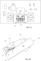
- FIG. 1A show an example 100 of a side emitting laser chip (single laser or laser array) 120 mounted on printed circuit board (PCB) 110, along with laser driver circuit components 140.
- the laser chip 120 is typically encapsulated with an encapsulating material 150, as shown by FIG. 1B .
- Laser light is emitted through a front surface 155 of the encapsulant 150.
- the front surface 155 is preferably smooth to provide a clean optical path for the laser, so the encapsulating material 150 must be either hard enough so the laser emitting surface (“front surface”) 155 may be polished or must be casted to optical quality.
- the encapsulation 150 is formed of hard epoxy using a dam and fill process. Uncured epoxy is applied over the laser array component 120. The epoxy material is soft enough to flow during application over the laser chip 120 upon the PCB 110.
- a two-step curing process is used to hold the location of the epoxy 150 to a desired portion of the PCB 110 and preventing the epoxy 150 from flowing elsewhere on the PCB 110 during an epoxy curing procedure.
- the first step of the two-step curing process uses ultraviolet (UV) cure epoxy 150 to perform an initial cure to partly solidify the epoxy 150 to fix (tack or hold) the epoxy 150 in shape, followed by a second step, for example a heat cure, to fully harden the epoxy 150.
- UV ultraviolet
- the epoxy essentially sits over the laser chip as applied, informally referred to as a "glob top.” After hardening, the light emitting side of the epoxy 150 is polished for better light transmission and light beam profile. Unfortunately, the polishable hard epoxy may create high stress in the laser chip 120.
- the contaminants in the encapsulant, including the cure agent may cause the degradation of the laser front facet in high temp and high humidity environment, eventually leading to degradation of the laser emitting front facet in conditions such as high temperatures (over 80C) and high humidity (over 80%).
- polish-able hard epoxy 150 to encapsulate the laser chip 120 on the PCB 110 creates undesirable residual stress on the laser chip 120 and may degrade the chip performance and create delamination of the epoxy 150 from a front facet of the laser chip 120. Therefore, there is a need in the industry to address one or more of the abovementioned shortcomings.
- WO 2020/107164 A1 proposes a laser diode packaging module.
- US 2020/144786 A1 proposes a quad flat no-leads package for a side emitting laser diode.
- US 6 784 511 B1 proposes a resin-sealed laser diode device.
- Embodiments of the present invention provide a method as set out in claim 1 and a chipboard assembly as set out in claim 9.
- the present invention is directed to a chip-onboard window assembly for a side-emitting laser chip mounted on a mounting surface of a printed circuit board (PCB).
- the window assembly includes a glass window and a window holding bracket.
- the bracket has a first walled portion, a second walled portion attached to the first walled portion, and a third walled portion opposite the second wall portion.
- the first walled portion further has a cutaway section configured to accommodate the glass window.
- An optical encapsulant covers the side-looking optical component.
- the glass window is attached to the side-looking optical component CoB assembly.
- substantially means “very nearly,” or within normal manufacturing tolerances.
- two planar surfaces described as substantially parallel may deviate from being perfectly parallel by a small angle within normal manufacturing tolerances, for example, less than 1 degree.
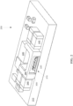
- FIG. 2 is a schematic diagram of an exemplary first embodiment 200 of a chip on board (CoB) package for a PCB mounted side emitting laser 220.
- the side emitting laser 220 is at least partially surrounded by a glass window assembly 300.
- Additional circuit components 240 are mounted outside an inner perimeter of the glass window assembly 300.
- the glass window assembly 300 includes a bracket portion 360 and a glass portion 370.
- the bracket portion 360 may be formed of, for example, plastic or ceramic.
- the bracket 360 has three walls 365 in a generally U-shaped profile (when viewed from above in a plane parallel to the PCB 210 ( FIG. 2 )), where the walls, when mounted on the PCB 210, are oriented substantially normal to the PCB 210.
- a substantially flat base portion 361 of the bracket 360 is configured to be attached to the PCB 210.
- a frame opening 362, or cutaway section, is positioned in a wall of the bracket 360.
- the frame opening 362 is sized to accommodate the glass portion 370.
- the glass 370 has a first planar surface 375 substantially parallel to a second planar surface 376.
- the first and second planar surfaces 375, 376 are bounded by a top edge 372 opposite a base edge 317, and two side edges 374.
- the glass 370 is substantially rectangular in profile, although the glass 370 may have other shapes in alternative embodiments.
- the glass 370 is affixed within the frame opening 362, for example, by a friction press fit (for example, within a V-groove in the bracket 360), or via an adhesive, such as epoxy.
- the glass 370 is disposed within the frame opening 362 of the bracket 360 such that the base edge 371 surface of the glass 370 is aligned with the bottom portion of the bracket 360, so that the glass window assembly 300 base is adjacent to the PCB 210 ( FIG. 2 ).
- the glass 370 may have an anti-reflective coating applied to one or both planar surfaces 375, 376.
- the glass 370 may be affixed to an interior or exterior surface of the bracket 360 with an adhesive.
- the glass 370 may be attached onto the laser chip on board (CoB) assembly, for example by epoxy, or by solder, for example, if the bracket bottom surface 361 is metalized and the PCB 210 metalized mounting pads to accommodate the glass window assembly 300.
- the glass window assembly 300 is mounted to the PCB 210, the glass 370 and the bracket 360 are either sealed against the PCB 210 or are attached sufficiently close to the PCB 210 to contain a potting compound described further below.
- the glass window assembly 300 (consisting of the glass 370 and holding bracket 360) is mounted onto the PCB 210 with the side emitting laser 220 disposed inside the glass window assembly 300.
- the glass window assembly 300 and the side emitting laser 220 are arranged so the side emitting laser 220 emits a beam directed through the glass 370.
- the side emitting laser 220 is then potted to cover the side emitting laser 220 and any associated wire bonds with an optical encapsulant having of low stress and low contaminant properties.
- a potting compound (encapsulant) to encapsulate the side emitting laser 220 may use an encapsulant that need not be hard (for polishing) and/or UV curable with UV cure agents to contain flow, such as electrical joint compound (EJC) silicone, as the glass window assembly 300 serves to contain the potting compound in the vicinity of the side emitting laser 220.
- EJC electrical joint compound
- the glass window assembly 300 has an open back design, such that the glass window assembly 300 does not physically restrict flow of the potting compound 455 through a rear opening 364.
- the potting compound 455 may be contained within the glass window assembly by applying the uncured potting compound 455 within the glass window assembly when a top planar surface of PCB 210 (that the glass window assembly 300 and the side emitting laser 220 are mounted to) is oriented at an angle during application and while the potting compound is cured.
- the angle ⁇ may be in the range of 30° to 45 °.
- the top surface of the potting compound 455 (shown as a dashed line in FIG. 4 ) is oriented at the angle ⁇ with respect to the top planar surface of the PCB 210.
- Table 1 shows a comparison between a previous "glob top” laser assembly ( FIG. 1B ) and the first embodiment ( FIG. 2 ) having a glass window. Table 1: Comparison of first embodiment with previous approaches Existing "Glob Top” Glass Window Material Selection Epoxy: UV cure + heat cure: may have ionic contaminations.
- EJC silicone or epoxy 'clean' version and heat cure only Mechanical property Hard (for polishing) Soft (new material Shore A hardness 30, low residual stress, no polishing cost, no polishing yield loss, no polishing stress)
- Hard for polishing
- Soft new material Shore A hardness 30, low residual stress, no polishing cost, no polishing yield loss, no polishing stress
- Optical performance Light transmission loss from epoxy to air (AR coating not possible on epoxy surface) AR coated window (lower light loss, higher efficiency) Quality and Reliability Higher optical power output (with AR coated window), longer laser working lifetime (with lower stress), more stable performance in high temperature and high humidity environment
- a surrounding glass window assembly 560 includes a back wall 580 entirely surrounding the laser chip 220, so the potting compound may be applied over the laser chip 220 such that the potting compound is constrained from flowing outside the surrounding window glass assembly. Under the second embodiment, the potting compound may be applied without inclining the PCB 210 with respect to horizontal.
- the first embodiment may be preferable when external components 240, for example, MOSFET, capacitors, and/or resistors are sufficiently close to the laser chip 220 so there is not room for a closed holder.
- external components 240 for example, MOSFET, capacitors, and/or resistors
- the optical encapsulant may be filled as usual from the top to fill the holder to cover the laser chip 220 and wire bonds without tilting the CoB, such that the surface of the optical encapsulant is substantially parallel to the PCB 210.
- FIG. 6 is a flowchart of an exemplary method for encapsulating a side-looking optical component mounted on a sub-portion of a printed circuit board (PCB) of a chip-onboard (CoB) assembly.
- PCB printed circuit board
- CoB chip-onboard
- a glass window 370 is provided, as shown by block 610.
- a window holding bracket 360 is provided, as shown by block 620.
- the holding bracket includes three walled portions 365: a first walled portion, a second walled portion attached to the first walled portion, and a third walled portion attached to the first wall portion opposite and substantially parallel to the second walled portion.
- the first walled portion has a cutaway section 362 configured to accommodate the glass window 370.
- the glass window 370 is attached into the cutaway section 362 of the window holding bracket 360, as shown by block 630.
- the glass window holding bracket 360 is attached to the PCB 210, as shown by block 640.
- the laser chip 220 and wire bonds 425 ( FIG. 4 ) are covered with an optical encapsulant 455 ( FIG 4 ), as shown by block 660.
- the glass 370 may be affixed to the bracket 700 in other ways.
- the glass window 370 may be attached to an outer surface of the bracket 760.
- the glass window assembly 300 includes a bracket portion 760 and a glass portion 370.
- the bracket portion 760 may be formed of, for example, plastic or ceramic.
- the bracket 760 has three walls 765 in a generally U-shaped profile (when viewed from above in a plane parallel to the PCB 210 ( FIG. 2 )), where the walls, when mounted on the PCB 210, are oriented substantially normal to the PCB 210.
- a substantially flat base portion 761 of the bracket 760 is configured to be attached to the PCB 210.
- a frame opening 762, or cutaway section, is positioned in a front wall of the bracket 760.
- the front wall of the bracket 760 is configured to receive the glass portion 370 so the glass portion is attached, for example with an adhesive, to cover the frame opening 762.
- the PCB 210 may include a recessed portion 810 sized to accommodate a base edge 371 of the window 370 extending below the base portion 761 of the bracket 760.
- the glass window assembly 700 may optionally include a (fourth) back wall 780 to entire surrounding the laser chip 220, so the potting compound may be applied over the laser chip 220 and wire bonds 425 such that the potting compound is constrained from flowing outside the surrounding window glass assembly 700.
- the optional back wall 780 may be omitted from the window glass assembly 700, as shown by FIG. 9A .
- the potting compound 455 may be applied over the laser chip 220 and wire bonds 425 by inclining the PCB 210 with respect to horizontal (with a board incline angle ⁇ in a range of, for example, 25°-50°). After the potting compound 455 has cured, the PCB 210 may be returned to a horizontal orientation and the potting compound 455 remains substantially within the window glass assembly 700.
- the bracket 760 may attached to the PCB 210 without the glass window 97, where the glass window 370 is attached to the PCB 210 and/or the bracket 760 after the bracket 760 has been attached to the PCB 210.
- the glass window 370 may be attached to the PCB 210 and/or the bracket 760, for example, by an adhesive.
- FIGS. 10-12 show an alternative embodiment based on the first embodiment where the window 370 is inset into the bracket 360, and the base of the window 370 is extended below the floor of the bracket 360 into a recess 810 in the PCB 210.
- FIG. 13 shows a variation of the package of FIG. 5 with the window extending below the bracket into a recess on the PCB.
- the package may in addition accommodate other side-looking optical components, such as sensors or detectors.
Landscapes
- Physics & Mathematics (AREA)
- Condensed Matter Physics & Semiconductors (AREA)
- General Physics & Mathematics (AREA)
- Electromagnetism (AREA)
- Optics & Photonics (AREA)
- Semiconductor Lasers (AREA)
Claims (15)
- Verfahren zum Einkapseln eines seitlich emittierenden Laserchips (220), der auf einem Teilabschnitt einer Leiterplatte, PCB, einer Nacktchipmontage-,CoB,-Anordnung (200) angebracht ist, umfassend die folgenden Schritte:Bereitstellen eines Glasfensters (370);Bereitstellen einer Fensterhalterung (360, 760), umfassend einen ersten Wandabschnitt, einen zweiten Wandabschnitt, der an dem ersten Wandabschnitt befestigt ist, und einen dem zweiten Wandabschnitt gegenüberliegenden dritten Wandabschnitt, der an dem ersten Wandabschnitt befestigt ist, wobei der erste Wandabschnitt ferner einen ausgeschnittenen Abschnitt (362, 762) umfasst, der ausgelegt ist, um das Glasfenster aufzunehmen:Anbringen des Glasfensters an der Fensterhalterung, um den ausgeschnittenen Abschnitt des ersten Wandteils zu bedecken und/oder zu füllen;Befestigen der Fensterhalterung an der PCB der CoB-Anordnung, sodass der seitlich emittierende Laserchip benachbart zu dem ersten Wandabschnitt und zwischen dem zweiten und dritten Wandabschnitt angeordnet ist, und sodass eine Bodenfläche des Glasfensters auf einer Oberfläche der PCB angeordnet ist; undnach dem Befestigen der Fensterhalterung an der PCB, Aufbringen eines optischen Einkapselungsmittels (455), um den seitlich emittierenden Laserchip zu bedecken.
- Verfahren nach Anspruch 1, wobei das optische Einkapselungsmittel kein UV-Härtungsmittel und/oder ionische Verunreinigungen enthält.
- Verfahren nach Anspruch 1, das ferner den Schritt des Aufbringens einer antireflektierenden Beschichtung umfasst, die auf zumindest eine Fläche des Glasfensters aufgebracht wird.
- Verfahren nach Anspruch 1, wobei das optische Einkapselungsmittel einen Spalt zwischen dem seitlich emittierenden Laserchip und dem Glasfenster füllt.
- Verfahren nach Anspruch 1, das ferner den Schritt des Anordnens der CoB-Anordnung in einem Winkel α in Bezug auf die Horizontale vor dem Aufbringen des optischen Einkapselungsmittels umfasst.
- Verfahren nach Anspruch 5, wobei der Winkel α im Bereich von 30° bis 45° liegt.
- Verfahren nach Anspruch 1, wobei die Halterung ferner einen vierten Wandabschnitt (580; 780) umfasst, der gegenüberliegend zu und im Wesentlichen parallel zu dem ersten Wandabschnitt angeordnet und an dem zweiten Wandabschnitt und dem dritten Wandabschnitt angebracht ist.
- Verfahren nach Anspruch 1, das ferner den Schritt des Bereitstellens einer Vertiefung (810) in der PCB zum Aufnehmen des Glasfensters umfasst.
- Nacktchipmontage-, CoB-, Anordnung (200), einschließlich eines seitlich emittierenden Laserchips (220), der auf einer Befestigungsoberfläche einer Leiterplatte, PCB, (210) befestigt ist, die Folgendes umfasst:eine auf der PCB befestigte Glasfensteranordnung (300), die ferner Folgendes umfasst:ein Glasfenster (370); undeine Fensterhalterung (360; 760), umfassend einen ersten Wandabschnitt, einen zweiten Wandabschnitt, der an dem ersten Wandabschnitt befestigt ist, und einen dem zweiten Wandabschnitt gegenüberliegenden dritten Wandabschnitt, der an dem ersten Wandabschnitt befestigt ist, wobei der erste Wandabschnitt ferner einen ausgeschnittenen Abschnitt (362; 702) umfasst, der ausgelegt ist, um das Glasfenster aufzunehmen; undein optisches Einkapselungsmittel (455), das den seitlich emittierenden Laserchip bedeckt und einen Spalt zwischen dem seitlich emittierenden Laserchip und dem Glasfenster füllt, wobei:der seitlich emittierende Laserchip angrenzend an den ersten Wandabschnitt und zwischen dem zweiten und dritten Wandabschnitt angeordnet ist, undeine Bodenfläche des Glasfensters auf einer Oberfläche der PCB angeordnet ist.
- CoB-Anordnung nach Anspruch 9, wobei zumindest eine Fläche des Glasfensters eine antireflektive Beschichtung umfasst.
- CoB-Anordnung nach Anspruch 9, wobei eine Oberseite des Einkapselungsmittels in einem Winkel α im Bereich von 30° bis 45° in Bezug auf eine ebene Befestigungsoberfläche der PCB ausgerichtet ist.
- CoB-Anordnung nach Anspruch 9, wobei die Halterung ferner einen vierten Wandabschnitt (580; 780) umfasst, der gegenüberliegend zu und im Wesentlichen parallel zu dem ersten Wandabschnitt angeordnet und an dem zweiten Wandabschnitt und dem dritten Wandabschnitt angebracht ist.
- CoB-Anordnung nach Anspruch 12, wobei das optische Einkapselungsmittel in einem Bereich auf der PCB begrenzt ist, der durch den ersten, zweiten, dritten und vierten Wandabschnitt eingegrenzt ist.
- CoB-Anordnung nach Anspruch 9, wobei die PCB eine Vertiefung (810) umfasst, die ausgelegt ist, um den Bodenabschnitt des Glasfensters aufzunehmen.
- CoB-Anordnung nach Anspruch 9, wobei der dritte Wandabschnitt im Wesentlichen parallel zu dem zweiten Wandabschnitt angeordnet ist.
Applications Claiming Priority (2)
| Application Number | Priority Date | Filing Date | Title |
|---|---|---|---|
| US202063109451P | 2020-11-04 | 2020-11-04 | |
| PCT/US2021/057816 WO2022098694A1 (en) | 2020-11-04 | 2021-11-03 | Semiconductor side emitting laser on board package and method forming same |
Publications (2)
| Publication Number | Publication Date |
|---|---|
| EP4241349A1 EP4241349A1 (de) | 2023-09-13 |
| EP4241349B1 true EP4241349B1 (de) | 2024-08-14 |
Family
ID=78771238
Family Applications (1)
| Application Number | Title | Priority Date | Filing Date |
|---|---|---|---|
| EP21815050.6A Active EP4241349B1 (de) | 2020-11-04 | 2021-11-03 | Halbleiterseitenemittierender laser auf einer leiterplattenverpackung und herstellungsverfahren dafür |
Country Status (3)
| Country | Link |
|---|---|
| US (1) | US20230268711A1 (de) |
| EP (1) | EP4241349B1 (de) |
| WO (1) | WO2022098694A1 (de) |
Families Citing this family (1)
| Publication number | Priority date | Publication date | Assignee | Title |
|---|---|---|---|---|
| JP7659183B2 (ja) * | 2021-06-25 | 2025-04-09 | 日亜化学工業株式会社 | レーザ光源 |
Family Cites Families (5)
| Publication number | Priority date | Publication date | Assignee | Title |
|---|---|---|---|---|
| US6784511B1 (en) * | 1994-01-20 | 2004-08-31 | Fuji Electric Co., Ltd. | Resin-sealed laser diode device |
| DE102015114292A1 (de) * | 2015-08-27 | 2017-03-02 | Osram Opto Semiconductors Gmbh | Laserbauelement und Verfahren zu seiner Herstellung |
| DE102015115824A1 (de) * | 2015-09-18 | 2017-03-23 | Osram Opto Semiconductors Gmbh | Optoelektronisches Bauelement |
| EP3874566A1 (de) * | 2018-11-01 | 2021-09-08 | Excelitas Canada Inc. | Quad flat no-leads package für seitlich abstrahlende laserdiode |
| WO2020107164A1 (zh) * | 2018-11-26 | 2020-06-04 | 深圳市大疆创新科技有限公司 | 激光二极管封装模块及距离探测装置、电子设备 |
-
2021
- 2021-11-03 WO PCT/US2021/057816 patent/WO2022098694A1/en not_active Ceased
- 2021-11-03 EP EP21815050.6A patent/EP4241349B1/de active Active
-
2023
- 2023-05-02 US US18/310,967 patent/US20230268711A1/en active Pending
Also Published As
| Publication number | Publication date |
|---|---|
| WO2022098694A1 (en) | 2022-05-12 |
| US20230268711A1 (en) | 2023-08-24 |
| EP4241349A1 (de) | 2023-09-13 |
Similar Documents
| Publication | Publication Date | Title |
|---|---|---|
| US5650915A (en) | Thermally enhanced molded cavity package having a parallel lid | |
| US12317657B2 (en) | Optical semiconductor element mounting package and optical semiconductor device using the same | |
| US7458703B2 (en) | Light emitting diode package having dual lens structure for lateral light emission | |
| JP5128047B2 (ja) | 光デバイス及び光デバイスの生産方法 | |
| TWI382561B (zh) | 附有反射透鏡之功率發光二極體封裝及其製造方法 | |
| US7671534B2 (en) | Liquid crystal display, illuminant module and its manufacturing method | |
| US7446347B2 (en) | Optoelectronic component and method for the production thereof, module and device comprising a module of this type | |
| US8334585B2 (en) | LED package and fabrication method thereof | |
| EP2447989A1 (de) | Halbleitergehäuse und montagestruktur für ein halbleitergehäuse | |
| KR19990013833A (ko) | 반도체장치 및 그의 제조방법 | |
| US7193299B2 (en) | Conductor frame and housing for a radiation-emitting component, radiation-emitting component and display and/or illumination system using radiation-emitting components | |
| EP2128905A2 (de) | Lichtemittierendes Halbleiterbauelement | |
| JP4571320B2 (ja) | 半導体チップパッケージ | |
| GB2413896A (en) | Optoelectronic surface mount package | |
| JP2008244143A (ja) | 半導体発光装置の製造方法 | |
| US7371603B2 (en) | Method of fabricating light emitting diode package | |
| US20230268711A1 (en) | Semiconductor side emitting laser on board package and method forming same | |
| US7309916B2 (en) | Semiconductor package and method for its manufacture | |
| US20200144786A1 (en) | Quad Flat No-leads Package for Side Emitting Laser Diode | |
| US7178235B2 (en) | Method of manufacturing an optoelectronic package | |
| US20050167773A1 (en) | Semiconductor element for solid state image sensing device and solid state image sensing device using the same | |
| US7705437B2 (en) | Semiconductor device | |
| JP4166759B2 (ja) | 光学装置のパッケージ構造体の製造方法 | |
| US7135768B2 (en) | Hermetic seal | |
| US20030113076A1 (en) | Optical electronic device |
Legal Events
| Date | Code | Title | Description |
|---|---|---|---|
| STAA | Information on the status of an ep patent application or granted ep patent |
Free format text: STATUS: UNKNOWN |
|
| STAA | Information on the status of an ep patent application or granted ep patent |
Free format text: STATUS: THE INTERNATIONAL PUBLICATION HAS BEEN MADE |
|
| PUAI | Public reference made under article 153(3) epc to a published international application that has entered the european phase |
Free format text: ORIGINAL CODE: 0009012 |
|
| STAA | Information on the status of an ep patent application or granted ep patent |
Free format text: STATUS: REQUEST FOR EXAMINATION WAS MADE |
|
| 17P | Request for examination filed |
Effective date: 20230531 |
|
| AK | Designated contracting states |
Kind code of ref document: A1 Designated state(s): AL AT BE BG CH CY CZ DE DK EE ES FI FR GB GR HR HU IE IS IT LI LT LU LV MC MK MT NL NO PL PT RO RS SE SI SK SM TR |
|
| DAV | Request for validation of the european patent (deleted) | ||
| DAX | Request for extension of the european patent (deleted) | ||
| GRAP | Despatch of communication of intention to grant a patent |
Free format text: ORIGINAL CODE: EPIDOSNIGR1 |
|
| STAA | Information on the status of an ep patent application or granted ep patent |
Free format text: STATUS: GRANT OF PATENT IS INTENDED |
|
| RIC1 | Information provided on ipc code assigned before grant |
Ipc: H01S 5/02208 20210101ALN20240227BHEP Ipc: H01S 5/40 20060101ALN20240227BHEP Ipc: H01S 5/02326 20210101ALI20240227BHEP Ipc: H01S 5/02257 20210101AFI20240227BHEP |
|
| INTG | Intention to grant announced |
Effective date: 20240322 |
|
| GRAS | Grant fee paid |
Free format text: ORIGINAL CODE: EPIDOSNIGR3 |
|
| GRAA | (expected) grant |
Free format text: ORIGINAL CODE: 0009210 |
|
| STAA | Information on the status of an ep patent application or granted ep patent |
Free format text: STATUS: THE PATENT HAS BEEN GRANTED |
|
| P01 | Opt-out of the competence of the unified patent court (upc) registered |
Free format text: CASE NUMBER: APP_34021/2024 Effective date: 20240606 |
|
| AK | Designated contracting states |
Kind code of ref document: B1 Designated state(s): AL AT BE BG CH CY CZ DE DK EE ES FI FR GB GR HR HU IE IS IT LI LT LU LV MC MK MT NL NO PL PT RO RS SE SI SK SM TR |
|
| REG | Reference to a national code |
Ref country code: GB Ref legal event code: FG4D |
|
| REG | Reference to a national code |
Ref country code: CH Ref legal event code: EP |
|
| REG | Reference to a national code |
Ref country code: DE Ref legal event code: R096 Ref document number: 602021017325 Country of ref document: DE |
|
| REG | Reference to a national code |
Ref country code: IE Ref legal event code: FG4D |
|
| REG | Reference to a national code |
Ref country code: LT Ref legal event code: MG9D |
|
| REG | Reference to a national code |
Ref country code: NL Ref legal event code: MP Effective date: 20240814 |
|
| PG25 | Lapsed in a contracting state [announced via postgrant information from national office to epo] |
Ref country code: NO Free format text: LAPSE BECAUSE OF FAILURE TO SUBMIT A TRANSLATION OF THE DESCRIPTION OR TO PAY THE FEE WITHIN THE PRESCRIBED TIME-LIMIT Effective date: 20241114 |
|
| REG | Reference to a national code |
Ref country code: AT Ref legal event code: MK05 Ref document number: 1714176 Country of ref document: AT Kind code of ref document: T Effective date: 20240814 |
|
| PG25 | Lapsed in a contracting state [announced via postgrant information from national office to epo] |
Ref country code: FI Free format text: LAPSE BECAUSE OF FAILURE TO SUBMIT A TRANSLATION OF THE DESCRIPTION OR TO PAY THE FEE WITHIN THE PRESCRIBED TIME-LIMIT Effective date: 20240814 Ref country code: GR Free format text: LAPSE BECAUSE OF FAILURE TO SUBMIT A TRANSLATION OF THE DESCRIPTION OR TO PAY THE FEE WITHIN THE PRESCRIBED TIME-LIMIT Effective date: 20241115 Ref country code: PT Free format text: LAPSE BECAUSE OF FAILURE TO SUBMIT A TRANSLATION OF THE DESCRIPTION OR TO PAY THE FEE WITHIN THE PRESCRIBED TIME-LIMIT Effective date: 20241216 Ref country code: PL Free format text: LAPSE BECAUSE OF FAILURE TO SUBMIT A TRANSLATION OF THE DESCRIPTION OR TO PAY THE FEE WITHIN THE PRESCRIBED TIME-LIMIT Effective date: 20240814 Ref country code: NL Free format text: LAPSE BECAUSE OF FAILURE TO SUBMIT A TRANSLATION OF THE DESCRIPTION OR TO PAY THE FEE WITHIN THE PRESCRIBED TIME-LIMIT Effective date: 20240814 |
|
| PG25 | Lapsed in a contracting state [announced via postgrant information from national office to epo] |
Ref country code: BG Free format text: LAPSE BECAUSE OF FAILURE TO SUBMIT A TRANSLATION OF THE DESCRIPTION OR TO PAY THE FEE WITHIN THE PRESCRIBED TIME-LIMIT Effective date: 20240814 |
|
| PG25 | Lapsed in a contracting state [announced via postgrant information from national office to epo] |
Ref country code: LV Free format text: LAPSE BECAUSE OF FAILURE TO SUBMIT A TRANSLATION OF THE DESCRIPTION OR TO PAY THE FEE WITHIN THE PRESCRIBED TIME-LIMIT Effective date: 20240814 |
|
| PG25 | Lapsed in a contracting state [announced via postgrant information from national office to epo] |
Ref country code: IS Free format text: LAPSE BECAUSE OF FAILURE TO SUBMIT A TRANSLATION OF THE DESCRIPTION OR TO PAY THE FEE WITHIN THE PRESCRIBED TIME-LIMIT Effective date: 20241214 Ref country code: AT Free format text: LAPSE BECAUSE OF FAILURE TO SUBMIT A TRANSLATION OF THE DESCRIPTION OR TO PAY THE FEE WITHIN THE PRESCRIBED TIME-LIMIT Effective date: 20240814 |
|
| PG25 | Lapsed in a contracting state [announced via postgrant information from national office to epo] |
Ref country code: HR Free format text: LAPSE BECAUSE OF FAILURE TO SUBMIT A TRANSLATION OF THE DESCRIPTION OR TO PAY THE FEE WITHIN THE PRESCRIBED TIME-LIMIT Effective date: 20240814 |
|
| PG25 | Lapsed in a contracting state [announced via postgrant information from national office to epo] |
Ref country code: ES Free format text: LAPSE BECAUSE OF FAILURE TO SUBMIT A TRANSLATION OF THE DESCRIPTION OR TO PAY THE FEE WITHIN THE PRESCRIBED TIME-LIMIT Effective date: 20240814 Ref country code: RS Free format text: LAPSE BECAUSE OF FAILURE TO SUBMIT A TRANSLATION OF THE DESCRIPTION OR TO PAY THE FEE WITHIN THE PRESCRIBED TIME-LIMIT Effective date: 20241114 |
|
| PG25 | Lapsed in a contracting state [announced via postgrant information from national office to epo] |
Ref country code: RS Free format text: LAPSE BECAUSE OF FAILURE TO SUBMIT A TRANSLATION OF THE DESCRIPTION OR TO PAY THE FEE WITHIN THE PRESCRIBED TIME-LIMIT Effective date: 20241114 Ref country code: PT Free format text: LAPSE BECAUSE OF FAILURE TO SUBMIT A TRANSLATION OF THE DESCRIPTION OR TO PAY THE FEE WITHIN THE PRESCRIBED TIME-LIMIT Effective date: 20241216 Ref country code: PL Free format text: LAPSE BECAUSE OF FAILURE TO SUBMIT A TRANSLATION OF THE DESCRIPTION OR TO PAY THE FEE WITHIN THE PRESCRIBED TIME-LIMIT Effective date: 20240814 Ref country code: NO Free format text: LAPSE BECAUSE OF FAILURE TO SUBMIT A TRANSLATION OF THE DESCRIPTION OR TO PAY THE FEE WITHIN THE PRESCRIBED TIME-LIMIT Effective date: 20241114 Ref country code: NL Free format text: LAPSE BECAUSE OF FAILURE TO SUBMIT A TRANSLATION OF THE DESCRIPTION OR TO PAY THE FEE WITHIN THE PRESCRIBED TIME-LIMIT Effective date: 20240814 Ref country code: LV Free format text: LAPSE BECAUSE OF FAILURE TO SUBMIT A TRANSLATION OF THE DESCRIPTION OR TO PAY THE FEE WITHIN THE PRESCRIBED TIME-LIMIT Effective date: 20240814 Ref country code: IS Free format text: LAPSE BECAUSE OF FAILURE TO SUBMIT A TRANSLATION OF THE DESCRIPTION OR TO PAY THE FEE WITHIN THE PRESCRIBED TIME-LIMIT Effective date: 20241214 Ref country code: HR Free format text: LAPSE BECAUSE OF FAILURE TO SUBMIT A TRANSLATION OF THE DESCRIPTION OR TO PAY THE FEE WITHIN THE PRESCRIBED TIME-LIMIT Effective date: 20240814 Ref country code: GR Free format text: LAPSE BECAUSE OF FAILURE TO SUBMIT A TRANSLATION OF THE DESCRIPTION OR TO PAY THE FEE WITHIN THE PRESCRIBED TIME-LIMIT Effective date: 20241115 Ref country code: FI Free format text: LAPSE BECAUSE OF FAILURE TO SUBMIT A TRANSLATION OF THE DESCRIPTION OR TO PAY THE FEE WITHIN THE PRESCRIBED TIME-LIMIT Effective date: 20240814 Ref country code: ES Free format text: LAPSE BECAUSE OF FAILURE TO SUBMIT A TRANSLATION OF THE DESCRIPTION OR TO PAY THE FEE WITHIN THE PRESCRIBED TIME-LIMIT Effective date: 20240814 Ref country code: BG Free format text: LAPSE BECAUSE OF FAILURE TO SUBMIT A TRANSLATION OF THE DESCRIPTION OR TO PAY THE FEE WITHIN THE PRESCRIBED TIME-LIMIT Effective date: 20240814 Ref country code: AT Free format text: LAPSE BECAUSE OF FAILURE TO SUBMIT A TRANSLATION OF THE DESCRIPTION OR TO PAY THE FEE WITHIN THE PRESCRIBED TIME-LIMIT Effective date: 20240814 |
|
| PG25 | Lapsed in a contracting state [announced via postgrant information from national office to epo] |
Ref country code: RO Free format text: LAPSE BECAUSE OF FAILURE TO SUBMIT A TRANSLATION OF THE DESCRIPTION OR TO PAY THE FEE WITHIN THE PRESCRIBED TIME-LIMIT Effective date: 20240814 Ref country code: SM Free format text: LAPSE BECAUSE OF FAILURE TO SUBMIT A TRANSLATION OF THE DESCRIPTION OR TO PAY THE FEE WITHIN THE PRESCRIBED TIME-LIMIT Effective date: 20240814 Ref country code: DK Free format text: LAPSE BECAUSE OF FAILURE TO SUBMIT A TRANSLATION OF THE DESCRIPTION OR TO PAY THE FEE WITHIN THE PRESCRIBED TIME-LIMIT Effective date: 20240814 |
|
| PG25 | Lapsed in a contracting state [announced via postgrant information from national office to epo] |
Ref country code: EE Free format text: LAPSE BECAUSE OF FAILURE TO SUBMIT A TRANSLATION OF THE DESCRIPTION OR TO PAY THE FEE WITHIN THE PRESCRIBED TIME-LIMIT Effective date: 20240814 |
|
| PG25 | Lapsed in a contracting state [announced via postgrant information from national office to epo] |
Ref country code: CZ Free format text: LAPSE BECAUSE OF FAILURE TO SUBMIT A TRANSLATION OF THE DESCRIPTION OR TO PAY THE FEE WITHIN THE PRESCRIBED TIME-LIMIT Effective date: 20240814 |
|
| PG25 | Lapsed in a contracting state [announced via postgrant information from national office to epo] |
Ref country code: SK Free format text: LAPSE BECAUSE OF FAILURE TO SUBMIT A TRANSLATION OF THE DESCRIPTION OR TO PAY THE FEE WITHIN THE PRESCRIBED TIME-LIMIT Effective date: 20240814 Ref country code: IT Free format text: LAPSE BECAUSE OF FAILURE TO SUBMIT A TRANSLATION OF THE DESCRIPTION OR TO PAY THE FEE WITHIN THE PRESCRIBED TIME-LIMIT Effective date: 20240814 |
|
| REG | Reference to a national code |
Ref country code: DE Ref legal event code: R097 Ref document number: 602021017325 Country of ref document: DE |
|
| PLBE | No opposition filed within time limit |
Free format text: ORIGINAL CODE: 0009261 |
|
| STAA | Information on the status of an ep patent application or granted ep patent |
Free format text: STATUS: NO OPPOSITION FILED WITHIN TIME LIMIT |
|
| REG | Reference to a national code |
Ref country code: CH Ref legal event code: PL |
|
| PG25 | Lapsed in a contracting state [announced via postgrant information from national office to epo] |
Ref country code: MC Free format text: LAPSE BECAUSE OF FAILURE TO SUBMIT A TRANSLATION OF THE DESCRIPTION OR TO PAY THE FEE WITHIN THE PRESCRIBED TIME-LIMIT Effective date: 20240814 |
|
| PG25 | Lapsed in a contracting state [announced via postgrant information from national office to epo] |
Ref country code: LU Free format text: LAPSE BECAUSE OF NON-PAYMENT OF DUE FEES Effective date: 20241103 |
|
| REG | Reference to a national code |
Ref country code: CH Ref legal event code: PL |
|
| 26N | No opposition filed |
Effective date: 20250515 |
|
| PG25 | Lapsed in a contracting state [announced via postgrant information from national office to epo] |
Ref country code: CH Free format text: LAPSE BECAUSE OF NON-PAYMENT OF DUE FEES Effective date: 20241130 |
|
| REG | Reference to a national code |
Ref country code: BE Ref legal event code: MM Effective date: 20241130 |
|
| PG25 | Lapsed in a contracting state [announced via postgrant information from national office to epo] |
Ref country code: SE Free format text: LAPSE BECAUSE OF FAILURE TO SUBMIT A TRANSLATION OF THE DESCRIPTION OR TO PAY THE FEE WITHIN THE PRESCRIBED TIME-LIMIT Effective date: 20240814 |
|
| PG25 | Lapsed in a contracting state [announced via postgrant information from national office to epo] |
Ref country code: BE Free format text: LAPSE BECAUSE OF NON-PAYMENT OF DUE FEES Effective date: 20241130 |
|
| PG25 | Lapsed in a contracting state [announced via postgrant information from national office to epo] |
Ref country code: IE Free format text: LAPSE BECAUSE OF NON-PAYMENT OF DUE FEES Effective date: 20241103 |
|
| PGFP | Annual fee paid to national office [announced via postgrant information from national office to epo] |
Ref country code: DE Payment date: 20251128 Year of fee payment: 5 |
|
| PGFP | Annual fee paid to national office [announced via postgrant information from national office to epo] |
Ref country code: GB Payment date: 20251127 Year of fee payment: 5 |
|
| PGFP | Annual fee paid to national office [announced via postgrant information from national office to epo] |
Ref country code: FR Payment date: 20251125 Year of fee payment: 5 |
|
| PG25 | Lapsed in a contracting state [announced via postgrant information from national office to epo] |
Ref country code: HU Free format text: LAPSE BECAUSE OF FAILURE TO SUBMIT A TRANSLATION OF THE DESCRIPTION OR TO PAY THE FEE WITHIN THE PRESCRIBED TIME-LIMIT; INVALID AB INITIO Effective date: 20211103 |
|
| PG25 | Lapsed in a contracting state [announced via postgrant information from national office to epo] |
Ref country code: CY Free format text: LAPSE BECAUSE OF FAILURE TO SUBMIT A TRANSLATION OF THE DESCRIPTION OR TO PAY THE FEE WITHIN THE PRESCRIBED TIME-LIMIT; INVALID AB INITIO Effective date: 20211103 |