EP4238929B1 - Trägheitssensor und herstellungsverfahren dafür - Google Patents
Trägheitssensor und herstellungsverfahren dafür Download PDFInfo
- Publication number
- EP4238929B1 EP4238929B1 EP21902236.5A EP21902236A EP4238929B1 EP 4238929 B1 EP4238929 B1 EP 4238929B1 EP 21902236 A EP21902236 A EP 21902236A EP 4238929 B1 EP4238929 B1 EP 4238929B1
- Authority
- EP
- European Patent Office
- Prior art keywords
- conducting material
- material layer
- comb tooth
- cavity
- layer
- Prior art date
- Legal status (The legal status is an assumption and is not a legal conclusion. Google has not performed a legal analysis and makes no representation as to the accuracy of the status listed.)
- Active
Links
Images



Classifications
-
- G—PHYSICS
- G01—MEASURING; TESTING
- G01P—MEASURING LINEAR OR ANGULAR SPEED, ACCELERATION, DECELERATION, OR SHOCK; INDICATING PRESENCE, ABSENCE, OR DIRECTION, OF MOVEMENT
- G01P15/00—Measuring acceleration; Measuring deceleration; Measuring shock, i.e. sudden change of acceleration
- G01P15/02—Measuring acceleration; Measuring deceleration; Measuring shock, i.e. sudden change of acceleration by making use of inertia forces using solid seismic masses
- G01P15/08—Measuring acceleration; Measuring deceleration; Measuring shock, i.e. sudden change of acceleration by making use of inertia forces using solid seismic masses with conversion into electric or magnetic values
- G01P15/0802—Details
-
- B—PERFORMING OPERATIONS; TRANSPORTING
- B81—MICROSTRUCTURAL TECHNOLOGY
- B81C—PROCESSES OR APPARATUS SPECIALLY ADAPTED FOR THE MANUFACTURE OR TREATMENT OF MICROSTRUCTURAL DEVICES OR SYSTEMS
- B81C1/00—Manufacture or treatment of devices or systems in or on a substrate
- B81C1/00777—Preserve existing structures from alteration, e.g. temporary protection during manufacturing
- B81C1/00785—Avoid chemical alteration, e.g. contamination, oxidation or unwanted etching
- B81C1/00801—Avoid alteration of functional structures by etching, e.g. using a passivation layer or an etch stop layer
-
- B—PERFORMING OPERATIONS; TRANSPORTING
- B81—MICROSTRUCTURAL TECHNOLOGY
- B81C—PROCESSES OR APPARATUS SPECIALLY ADAPTED FOR THE MANUFACTURE OR TREATMENT OF MICROSTRUCTURAL DEVICES OR SYSTEMS
- B81C1/00—Manufacture or treatment of devices or systems in or on a substrate
- B81C1/00015—Manufacture or treatment of devices or systems in or on a substrate for manufacturing microsystems
- B81C1/00134—Manufacture or treatment of devices or systems in or on a substrate for manufacturing microsystems comprising flexible or deformable structures
-
- B—PERFORMING OPERATIONS; TRANSPORTING
- B81—MICROSTRUCTURAL TECHNOLOGY
- B81B—MICROSTRUCTURAL DEVICES OR SYSTEMS, e.g. MICROMECHANICAL DEVICES
- B81B3/00—Devices comprising flexible or deformable elements, e.g. comprising elastic tongues or membranes
- B81B3/0018—Structures acting upon the moving or flexible element for transforming energy into mechanical movement or vice versa, i.e. actuators, sensors, generators
- B81B3/0021—Transducers for transforming electrical into mechanical energy or vice versa
-
- B—PERFORMING OPERATIONS; TRANSPORTING
- B81—MICROSTRUCTURAL TECHNOLOGY
- B81C—PROCESSES OR APPARATUS SPECIALLY ADAPTED FOR THE MANUFACTURE OR TREATMENT OF MICROSTRUCTURAL DEVICES OR SYSTEMS
- B81C1/00—Manufacture or treatment of devices or systems in or on a substrate
- B81C1/00015—Manufacture or treatment of devices or systems in or on a substrate for manufacturing microsystems
- B81C1/00134—Manufacture or treatment of devices or systems in or on a substrate for manufacturing microsystems comprising flexible or deformable structures
- B81C1/0015—Cantilevers
-
- B—PERFORMING OPERATIONS; TRANSPORTING
- B81—MICROSTRUCTURAL TECHNOLOGY
- B81C—PROCESSES OR APPARATUS SPECIALLY ADAPTED FOR THE MANUFACTURE OR TREATMENT OF MICROSTRUCTURAL DEVICES OR SYSTEMS
- B81C1/00—Manufacture or treatment of devices or systems in or on a substrate
- B81C1/00015—Manufacture or treatment of devices or systems in or on a substrate for manufacturing microsystems
- B81C1/00134—Manufacture or treatment of devices or systems in or on a substrate for manufacturing microsystems comprising flexible or deformable structures
- B81C1/00166—Electrodes
-
- B—PERFORMING OPERATIONS; TRANSPORTING
- B81—MICROSTRUCTURAL TECHNOLOGY
- B81C—PROCESSES OR APPARATUS SPECIALLY ADAPTED FOR THE MANUFACTURE OR TREATMENT OF MICROSTRUCTURAL DEVICES OR SYSTEMS
- B81C1/00—Manufacture or treatment of devices or systems in or on a substrate
- B81C1/00436—Shaping materials, i.e. techniques for structuring the substrate or the layers on the substrate
- B81C1/00523—Etching material
-
- G—PHYSICS
- G01—MEASURING; TESTING
- G01P—MEASURING LINEAR OR ANGULAR SPEED, ACCELERATION, DECELERATION, OR SHOCK; INDICATING PRESENCE, ABSENCE, OR DIRECTION, OF MOVEMENT
- G01P15/00—Measuring acceleration; Measuring deceleration; Measuring shock, i.e. sudden change of acceleration
- G01P15/02—Measuring acceleration; Measuring deceleration; Measuring shock, i.e. sudden change of acceleration by making use of inertia forces using solid seismic masses
- G01P15/08—Measuring acceleration; Measuring deceleration; Measuring shock, i.e. sudden change of acceleration by making use of inertia forces using solid seismic masses with conversion into electric or magnetic values
- G01P15/125—Measuring acceleration; Measuring deceleration; Measuring shock, i.e. sudden change of acceleration by making use of inertia forces using solid seismic masses with conversion into electric or magnetic values by capacitive pick-up
-
- B—PERFORMING OPERATIONS; TRANSPORTING
- B81—MICROSTRUCTURAL TECHNOLOGY
- B81B—MICROSTRUCTURAL DEVICES OR SYSTEMS, e.g. MICROMECHANICAL DEVICES
- B81B2201/00—Specific applications of microelectromechanical systems
- B81B2201/02—Sensors
- B81B2201/0228—Inertial sensors
-
- B—PERFORMING OPERATIONS; TRANSPORTING
- B81—MICROSTRUCTURAL TECHNOLOGY
- B81B—MICROSTRUCTURAL DEVICES OR SYSTEMS, e.g. MICROMECHANICAL DEVICES
- B81B2203/00—Basic microelectromechanical structures
- B81B2203/01—Suspended structures, i.e. structures allowing a movement
- B81B2203/0136—Comb structures
-
- B—PERFORMING OPERATIONS; TRANSPORTING
- B81—MICROSTRUCTURAL TECHNOLOGY
- B81C—PROCESSES OR APPARATUS SPECIALLY ADAPTED FOR THE MANUFACTURE OR TREATMENT OF MICROSTRUCTURAL DEVICES OR SYSTEMS
- B81C2201/00—Manufacture or treatment of microstructural devices or systems
- B81C2201/01—Manufacture or treatment of microstructural devices or systems in or on a substrate
- B81C2201/0101—Shaping material; Structuring the bulk substrate or layers on the substrate; Film patterning
- B81C2201/0118—Processes for the planarization of structures
- B81C2201/0125—Blanket removal, e.g. polishing
-
- B—PERFORMING OPERATIONS; TRANSPORTING
- B81—MICROSTRUCTURAL TECHNOLOGY
- B81C—PROCESSES OR APPARATUS SPECIALLY ADAPTED FOR THE MANUFACTURE OR TREATMENT OF MICROSTRUCTURAL DEVICES OR SYSTEMS
- B81C2201/00—Manufacture or treatment of microstructural devices or systems
- B81C2201/01—Manufacture or treatment of microstructural devices or systems in or on a substrate
- B81C2201/0101—Shaping material; Structuring the bulk substrate or layers on the substrate; Film patterning
- B81C2201/0128—Processes for removing material
- B81C2201/013—Etching
- B81C2201/0132—Dry etching, i.e. plasma etching, barrel etching, reactive ion etching [RIE], sputter etching or ion milling
-
- B—PERFORMING OPERATIONS; TRANSPORTING
- B81—MICROSTRUCTURAL TECHNOLOGY
- B81C—PROCESSES OR APPARATUS SPECIALLY ADAPTED FOR THE MANUFACTURE OR TREATMENT OF MICROSTRUCTURAL DEVICES OR SYSTEMS
- B81C2201/00—Manufacture or treatment of microstructural devices or systems
- B81C2201/01—Manufacture or treatment of microstructural devices or systems in or on a substrate
- B81C2201/0101—Shaping material; Structuring the bulk substrate or layers on the substrate; Film patterning
- B81C2201/0128—Processes for removing material
- B81C2201/013—Etching
- B81C2201/0135—Controlling etch progression
- B81C2201/014—Controlling etch progression by depositing an etch stop layer, e.g. silicon nitride, silicon oxide, metal
-
- B—PERFORMING OPERATIONS; TRANSPORTING
- B81—MICROSTRUCTURAL TECHNOLOGY
- B81C—PROCESSES OR APPARATUS SPECIALLY ADAPTED FOR THE MANUFACTURE OR TREATMENT OF MICROSTRUCTURAL DEVICES OR SYSTEMS
- B81C2201/00—Manufacture or treatment of microstructural devices or systems
- B81C2201/01—Manufacture or treatment of microstructural devices or systems in or on a substrate
- B81C2201/0174—Manufacture or treatment of microstructural devices or systems in or on a substrate for making multi-layered devices, film deposition or growing
- B81C2201/019—Bonding or gluing multiple substrate layers
Definitions
- MEMS micro-electro-mechanical system
- a forming method of the inertial sensor generally includes: first providing a first substrate and a second substrate which are mutually bonded; and then, etching the second substrate to form a movable comb tooth structure and suspending the movable comb tooth structure above the first substrate.
- the inertial sensor prepared based on the existing process usually has the problem that side walls of comb teeth of the movable comb tooth structure are damaged.
- Inertial sensors according to the state of the art are known, for instance, from prior art documents CN 105 621 348 A , and EP 1 046 917 A2 .
- An objective of the present invention is to provide a forming method of an inertial sensor, so as to alleviate damage to side walls of comb teeth of a formed movable comb tooth structure.
- the present invention provides a forming method of an inertial sensor, according to claim 1, which includes:
- a thickness of the thin film layer is less than a depth of the trench.
- the forming method further includes: forming a plurality of electrodes on the second conducting material layer, where at least part of the plurality of electrodes are used for being electrically connected to the movable comb tooth structure.
- first openings are further formed in the first conducting material layer, and when etching the second conducting material layer, second openings are further formed in the second conducting material layer.
- the second openings communicate with the first openings to form separation openings, and the plurality of electrodes are electrically isolated from each other by the separation openings.
- the first substrate further includes a first base and a first insulating layer formed between the first base and the first conducting material layer.
- a first cavity is formed in the first conducting material layer, and after bonding the first conducting material layer and the second conducting material layer, the comb tooth region is suspended above the first cavity.
- the second conducting material layer is further provided with a cantilever region, a second cavity and a stopper are further formed in the first conducting material layer, and after bonding the first conducting material layer and the second conducting material layer, the second cavity and the stopper are both located directly under the cantilever region.
- the second substrate further includes a second base and a second insulating layer formed between the second base and the second conducting material layer.
- the forming method further includes: grinding the second base to partially remove the second base, then etching the remaining second base by an etching process, stopping etching at the second insulating layer, and then removing the second insulating layer to expose the second conducting material layer.
- the method for etching the second conducting material layer to form the movable comb tooth structure includes: adopting a plasma etching process for etching the second conducting material layer.
- Another objective of the present invention is to provide an inertial sensor, according to claim 11, which includes:
- a first cavity is further formed in the first conducting material layer, and the movable comb tooth structure is suspended above the first cavity.
- the second conducting material layer is further provided with a cantilever region, a second cavity and a stopper are further formed in the first conducting material layer, and the second cavity and the stopper are both located directly under the cantilever region.
- the trench is formed in the comb tooth region of the second conducting material layer, so that the movable comb tooth structure formed in the comb tooth region can be spaced from the first conducting material layer; and the thin film layer is further arranged at the bottom of the trench, and the thin film layer can be used for realizing etching blocking while etching the second conducting material layer, so that etching on the second conducting material layer can be stopped at the thin film layer without damaging the first conducting material layer below.
- the bottoms of the comb teeth of the movable comb tooth structure are all fixed to the thin film layer, thereby avoiding damage to the side walls of the comb teeth due to torsion of the comb teeth during etching.
- the thin film layer with a small thickness can be arranged, and thus, only a small etching amount is required for removing the thin film layer, and at this time, other film layers cannot be largely eroded, which is conducive to guaranteeing stability of modules in a device.
- Reference numerals are as follows: 100-first substrate; 110-first base; 120-first insulating layer; 130-first conducting material layer; 130a-first cavity; 130b-second cavity; 130c-first opening; 131-stopper; 200-second substrate; 210-second base; 220-second insulating layer; 230-second conducting material layer; 231-movable comb tooth structure; 230a-trench; 240-thin film layer; 400-electrode; 510-separation opening; 600-seal-capping base plate; 610-seal-capping cavity; and 700-bonding sealing ring.
- the present invention provides an inertial sensor and a forming method thereof.
- the forming method includes the following steps.
- Step S100 A first substrate with a first conducting material layer and a second substrate with a second conducting material layer are provided, a trench is formed in a surface of a comb tooth region of the second conducting material layer, and a thin film layer is further formed at a bottom of the trench.
- Step S200 The second conducting material layer and the first conducting material layer are mutually bonded.
- Step S300 At least the comb tooth region of the second conducting material layer is etched, etching is stopped at the thin film layer to form a movable comb tooth structure, and bottoms of comb teeth in the movable comb tooth structure are all fixed to the thin film layer.
- Step S400 The thin film layer is removed.
- the forming method of the inertial sensor may include the following step S100 to step S400.
- the detailed description is made below in combination with FIG. 1 and FIG. 2 to FIG. 8 .
- FIG. 1 is a schematic flowchart of a forming method of an inertial sensor according to an embodiment of the present invention
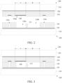
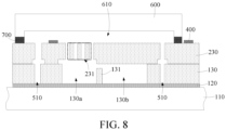
- FIG. 2 to FIG. 8 are schematic structural diagrams illustrating a preparation process of a forming method of an inertial sensor according to an embodiment of the present invention.
- step S100 referring to FIG. 2 for details, a first substrate 100 with a first conducting material layer 130 and a second substrate 200 with a second conducting material layer 230 are provided.
- a trench 230a is formed in a surface of a comb tooth region A of the second conducting material layer 230, and a thin film layer 240 is formed at a bottom of the trench 230a.
- a material of the thin film layer 240 includes silicon oxide, and the comb tooth region A of the second conducting material layer 230 is used for preparing the movable comb tooth structure.
- the thin film layer 240 is only located in the trench 230a, and a thickness of the thin film layer 240 is less than a depth of the trench 230a, so that a top surface of the thin film layer 240 is not higher than that of the second conducting material layer 230.
- the thickness of the thin film layer 240 may be only a half of the depth of the trench 230a, and the depth of the trench 230a is, for example, 0.5 ⁇ m-1.5 ⁇ m.
- the second conducting material layer 230 is further provided with a cantilever region B, the comb tooth region A is located beside the cantilever region B, and a part of the cantilever region B can constitute a mass block of the inertial sensor.
- a first cavity 130a is further formed in the first conducting material layer 130.
- the first cavity 130a corresponds to the comb tooth region A of the second conducting material layer 230 (i.e., after subsequent bonding of the first substrate 100 and the second substrate 200, the first cavity 130a is aligned with the comb tooth region A).
- a second cavity 130b is further formed in the first conducting material layer 130.
- the second cavity 130b corresponds to the cantilever region B of the second conducting material layer 230 (i.e., after subsequent bonding of the first substrate 100 and the second substrate 200, the second cavity 130b is aligned with the cantilever region B), thereby providing a vibration space for the cantilever region B.
- a stopper 131 may also be arranged in the first conducting material layer 130.
- the stopper 131 corresponds to the cantilever region B of the second conducting material layer 230, so as to limit a vibration range of the cantilever region B, and avoid the problems such as fracture due to excessive vibration of the cantilever region B.
- the stopper 131 is located below the cantilever region B, and in this embodiment, the stopper 131 may be further arranged on an edge of the second cavity 130b, so as to perform stopping from the edge of the cantilever region B. Further, a top surface of the stopper 131 is not higher than that of the first conducting material layer 130.
- a plurality of first openings 130c are further formed in the first conducting material layer 130, and the first openings 130c penetrate through the first conducting material layer 130.
- the first openings 130c are used for forming separation openings. It should be noted that in the constituted plurality of separation openings, part of the separation openings may also be used for forming alignment marks, thereby ensuring alignment precision of a subsequent patterning process. The detailed description will be made in subsequent steps.
- trenches and thin film layers are also formed in positions, corresponding to the first openings 130c, of the second conducting material layer 230.
- the first substrate 100 further includes a first base 110, and the first conducting material layer 130 is formed on the first base 110.
- a material of the first conducting material layer 130 for example, is an ion-doped silicon material, and a resistance value of the first conducting material layer 130 is, for example, between 0.01 ⁇ and 0.02 ⁇ .
- a first insulating layer 120 may also be formed on the first base 110.
- the first conducting material layer 130 is formed on the first insulating layer 120, and when etching the first conducting material layer 130 for patterning, the first insulating layer 120 may also be used as an etching stop layer.
- a material of the first insulating layer 120 includes silicon oxide.
- the specific process of bonding the second substrate 200 and the first substrate 100 is to mutually bond the first conducting material layer 130 in the first substrate 100 and the second conducting material layer 230 in the second substrate 200.
- both the first conducting material layer 130 and the second conducting material layer 230 are made of the ion-doped silicon material, that is, the first substrate 100 and the second substrate 200 are in silicon-silicon direct bonding, and the bonding process is simple and has high bonding force.
- the comb tooth region A of the second conducting material layer 230 corresponds to the first cavity 130a of the first conducting material layer 130, and thus, after bonding the first substrate 100 and the second substrate 200, the trench 230a is located above the first cavity 130a.
- the cantilever region B of the second conducting material layer 230 is located above the second cavity 130b.
- the second conducting material layer 230 is patterned to form the movable comb tooth structure.
- the second conducting material layer 230 further has the second insulating layer 220 and the second base 210, and thus, before patterning the second conducting material layer 230, the forming method further includes: the second base 210 and the second insulating layer 220 are removed.
- the method for removing the second base 210 and the second insulating layer 220 may include: firstly, the second base 210 is ground to partially remove the second base 210, then the remaining second base 210 is etched by an etching process, etching is stopped at the second insulating layer 220, and then the second insulating layer 220 is removed to expose the second conducting material layer 230.
- the remaining second base 210 can be etched by a plasma etching process, so as to improve etching precision of the second base 210.
- the second insulating layer 220 can be removed by a wet etching process.
- the material of the second insulating layer 220 may include silicon oxide, and thus, an etching agent adopted in the wet etching process for removing the second insulating layer 220 is, for example, hydrofluoric acid solution.
- the forming method before grinding the second base 210, the forming method further includes: a trim process is performed on an edge of the second base 210, so as to remove an edge part of the second base 210, and accordingly, when subsequently performing the grinding process on the second base 210, the problem that the edge part of the thinned second base 210 is suspended and is likely to fracture can be avoided.
- step S300 referring to FIG. 5 and FIG. 6 for details, at least the comb tooth region A of the second conducting material layer 230 is etched; etching is stopped at the thin film layer 240 to form the movable comb tooth structure 231; and the bottoms of the comb teeth in the movable comb tooth structure 231 are all fixed to the thin film layer 240.
- a pattern of the movable comb tooth structure can be defined by a second mask layer, and the second conducting material layer 230 is etched based on the second mask layer, so as to form the movable comb tooth structure 231, and the method, for example, includes the following steps.
- Step 1 Referring to FIG. 5 , a second mask layer 250 is formed on the second conducting material layer 230, and the pattern of the movable comb tooth structure is defined in the second mask layer 250.
- Step 2 Referring to FIG. 6 , the second conducting material layer 230 is etched with the second mask layer 250 as a mask, so as to form the movable comb tooth structure 231, and when etching the second conducting material layer 230, the thin film layer 240 is used as the etching stop layer to stop etching at the thin film layer 240.
- the method for etching the second conducting material layer 230 is, for example, to use the plasma etching process for etching the second conducting material layer 230, so as to improve the etching precision.
- the thin film layer 240 by arranging the thin film layer 240, on the one hand, the function of etching blocking can be realized, and accurate control over the etching process of the second conducting material layer 230 is improved; and on the other hand, based on the blocking of the thin film layer 240, a film layer below the thin film layer 240 can be effectively protected against etching damage.
- the bottoms of the comb teeth in the formed movable comb tooth structure 231 are all fixed to the thin film layer 240, and thus, as the etching process continues, a torsion space of the movable comb tooth structure 231 is released, but because all the comb teeth are fixed to the thin film layer 240, the comb teeth cannot twist at random, thereby avoiding damage to the side walls of the comb teeth due to torsion of the comb teeth during etching.
- a certain over etching amount can be generally increased, and the plasma etching process with higher precision can be adopted for etching.
- the comb teeth can be stably fixed by the thin film layer 240, and thus, even under the large etching amount, damage to the side walls of the comb teeth from plasma can still be effectively relieved.
- the forming method further includes: a plurality of electrodes 400 are formed on the second conducting material layer 230. At least part of the plurality of electrodes 400 are used for being electrically connected to the movable comb tooth structure 231.
- the plurality of electrodes 400 include two first electrodes which are electrically isolated from each other, and the two first electrodes are respectively electrically connected to two sets of comb teeth in the movable comb tooth structure 231.
- the plurality of electrodes 400 further include a second electrode, and the second electrode is used for being electrically connected to the cantilever region B of the second conducting material layer 230.
- the plurality of electrodes 400 can be electrically isolated from each other by separation openings 510. Specifically, through the separation openings 510, the first electrodes and the second electrode in the plurality of electrodes cannot be mutually connected by the conducting material layers (including the first conducting material layer 130 and the second conducting material layer 230).
- a forming method of the separation openings 510 may include: during patterning the second conducting material layer 230, second openings are further formed in the second conducting material layer 230, bottoms of the second openings are stopped at the thin film layer as well and located above the first openings 130c of the first conducting material layer 130, and thus, the first openings 130c and the second openings are in up-down mutual communication to form the separation openings 510, thereby utilizing the separation openings 510 for dividing the plurality of mutually separated electrodes.
- the drawings only exemplarily illustrate two separation openings 510 and two electrodes 400, and it should be understood that the electrodes 400 for connecting different modules are electrically isolated by the separation openings 510.
- the first electrodes can be electrically connected to the movable comb tooth structure 231, and the second electrode can be electrically connected to the cantilever region B through other interconnection structures.
- step S400 referring to FIG. 7 for details, the thin film layer 240 is removed.
- the forming method further includes: the second mask layer 250 is removed. At this time, the movable comb tooth structure 231 is suspended above the first cavity 130a.
- the thin film layer 240 is relatively thin, and thus, the thin film layer 240 can be depleted with a small etching amount. Specifically, the thin film layer 240 can be eroded by a gas phase corrosive agent. In this embodiment, the thin film layer 240 is removed by a vapor phase hydrogen fluoride (VHF) fumigation corrosion process. Compared with the wet etching process, the gas phase corrosive agent is utilized for eroding the thin film layer 240, which can effectively avoid the problems such as adhesion and torsion likely to occur between the adjacent comb teeth caused by corrosive liquid in the wet etching process.
- VHF vapor phase hydrogen fluoride
- the material of the first insulating layer 120 may be the same as that of the thin film layer 240 (e.g., both including silicon oxide), and accordingly, when etching the thin film layer 240, a trace amount of the first insulating layer 120 will be consumed.
- the etching amount of the thin film layer 240 is small, and thus, the first insulating layer 120 cannot be largely consumed, which is conducive to guaranteeing the stable supporting of the first insulating layer 120 to a film layer above the first insulating layer.
- the forming method of the inertial sensor further includes: a seal-capping base plate 600 is bonded onto the second conducting material layer 230.
- a seal-capping cavity 610 is formed in a surface, facing towards the second conducting material layer 230, of the seal-capping base plate 600, and the seal-capping cavity 610 faces the comb tooth region A and the cantilever region B.
- Part of the plurality of electrodes 400 may be sealed and capped within the seal-capping cavity 610, and the other part of electrodes may be located outside the seal-capping cavity 610 for electrically connecting an external circuit.
- the seal-capping base plate 600 and the second conducting material layer 230 may be specifically mutually bonded through two bonding rings.
- a first bonding ring is formed on a top surface, surrounding the seal-capping cavity 610, of the seal-capping base plate 600
- a second bonding ring is formed at a corresponding position of the second conducting material layer 230, and during bonding, the first bonding ring and the second bonding ring are mutually bonded and connected to form a bonding sealing ring 700.
- a first cavity 130a may also be formed in the first conducting material layer 130, and the movable comb tooth structure 231 is suspended above the first cavity 130a.
- the second conducting material layer 230 is further provided with a cantilever region B, and a second cavity 130b and a stopper 131 are further formed in the first conducting material layer 130.
- the second cavity 130b and the stopper 131 are both located directly under the cantilever region B.
- a top surface of the stopper 131 is lower than a bonding surface of the first conducting material layer 130.
- the end portion of the movable comb tooth structure 231 is contracted inward through the trench in the second conducting material layer 230, and thus, the movable comb tooth structure 231 can be suspended.
- this embodiment not only can guarantee that the movable comb tooth structure 231 is spaced from the second conducting material layer, but also can combine the thin film layer to further improve the quality of the formed comb tooth structure.
Landscapes
- Engineering & Computer Science (AREA)
- Manufacturing & Machinery (AREA)
- Microelectronics & Electronic Packaging (AREA)
- Physics & Mathematics (AREA)
- General Physics & Mathematics (AREA)
- Chemical & Material Sciences (AREA)
- Analytical Chemistry (AREA)
- Computer Hardware Design (AREA)
- Pressure Sensors (AREA)
- Micromachines (AREA)
- Gyroscopes (AREA)
Claims (13)
- Verfahren zum Ausbilden eines Trägheitssensors, umfassend:Bereitstellen eines ersten Substrats (100) mit einer ersten leitenden Materialschicht (130) und eines zweiten Substrats (200) mit einer zweiten leitenden Materialschicht (230), wobei die zweite leitende Materialschicht (230) einen Kammzahnbereich aufweist, ein Graben (230a) in einer Oberfläche des Kammzahnbereichs ausgebildet ist und ferner eine Dünnfilmschicht (240) an einem Boden des Grabens (230a) ausgebildet ist;gegenseitiges Verbinden der zweiten leitenden Materialschicht (230) und der ersten leitenden Materialschicht (130); undÄtzen zumindest des Kammzahnbereichs der zweiten leitenden Materialschicht (230) und Stoppen des Ätzens an der Dünnfilmschicht (240), um eine bewegliche Kammzahnstruktur (231) auszubilden, wobei Böden von Kammzähnen in der beweglichen Kammzahnstruktur (231) alle an der Dünnfilmschicht (240) befestigt sind; undEntfernen der Dünnfilmschicht (240).
- Verfahren zum Ausbilden des Trägheitssensors nach Anspruch 1, wobei eine Dicke der Dünnfilmschicht (240) geringer als eine Tiefe des Grabens (230a) ist.
- Verfahren zum Ausbilden des Trägheitssensors nach Anspruch 1, wobei nach dem Verbinden der zweiten leitenden Materialschicht (230) und der ersten leitenden Materialschicht (130) das Verfahren zum Ausbilden ferner umfasst:
Ausbilden mehrerer Elektroden (400) auf der zweiten leitenden Materialschicht (230), wobei zumindest ein Teil der mehreren Elektroden (400) verwendet wird, um elektrisch mit der beweglichen Kammzahnstruktur (231) verbunden zu werden. - Verfahren zum Ausbilden des Trägheitssensors nach Anspruch 3, wobei ferner erste Öffnungen (130c) in der ersten leitenden Materialschicht (130) ausgebildet werden, und wenn die zweite leitende Materialschicht (230) geätzt wird, ferner zweite Öffnungen in der zweiten leitenden Materialschicht (230) ausgebildet werden, wobei die zweiten Öffnungen mit den ersten Öffnungen (130c) in Verbindung stehen, um Trennöffnungen (510) auszubilden, und die mehreren Elektroden (400) durch die Trennöffnungen (510) elektrisch voneinander isoliert sind.
- Verfahren zum Ausbilden des Trägheitssensors nach Anspruch 1, wobei das erste Substrat (100) ferner eine erste Basis (110) und eine erste Isolierschicht (120), die zwischen der ersten Basis (110) und der ersten leitenden Materialschicht (130) ausgebildet ist, umfasst, und ferner ein erster Hohlraum (130a), der die erste Isolierschicht (120) freilegt, ein zweiter Hohlraum (130b) und ein Stopper (131), der sich auf der ersten Isolierschicht (120) befindet, in der ersten leitenden Materialschicht (130) ausgebildet sind.
- Verfahren zum Ausbilden des Trägheitssensors nach Anspruch 5, wobei ein Material der Dünnfilmschicht (240) das gleiche wie das der ersten Isolierschicht (120) ist.
- Verfahren zum Ausbilden des Trägheitssensors nach Anspruch 1, wobei ein erster Hohlraum (130a) in der ersten leitenden Materialschicht (130) ausgebildet ist und nach dem Verbinden der ersten leitenden Materialschicht (130) und der zweiten leitenden Materialschicht (230) der Kammzahnbereich über dem ersten Hohlraum (130a) aufgehängt ist und ein unterer Teil des Kammzahnbereichs dem ersten Hohlraum (130a) entspricht.
- Verfahren zum Ausbilden des Trägheitssensors nach Anspruch 1, wobei die zweite leitende Materialschicht (230) ferner mit einem freitragenden Bereich versehen ist, ferner ein zweiter Hohlraum (130b) und ein Stopper (131) in der ersten leitenden Materialschicht (130) ausgebildet sind und nach dem Verbinden der ersten leitenden Materialschicht (130) und der zweiten leitenden Materialschicht (230) der zweite Hohlraum (130b) und der Stopper (131) beide direkt unter dem freitragenden Bereich angeordnet sind und ein unterer Teil des freitragenden Bereichs dem zweiten Hohlraum (130b) entspricht.
- Verfahren zum Ausbilden des Trägheitssensors nach Anspruch 1, wobei das zweite Substrat (200) ferner eine zweite Basis (210) und eine zweite Isolierschicht (220) umfasst, die zwischen der zweiten Basis (210) und der zweiten leitenden Materialschicht (230) ausgebildet ist; und
vor dem Ätzen der zweiten leitenden Materialschicht (230) das Verfahren zum Ausbilden ferner umfasst: Schleifen der zweiten Basis (210), um die zweite Basis (210) teilweise zu entfernen, dann Ätzen der verbleibenden zweiten Basis (210) durch einen Ätzprozess, Stoppen des Ätzens an der zweiten Isolierschicht (220) und dann Entfernen der zweiten Isolierschicht (220), um die zweite leitende Materialschicht (230) freizulegen. - Verfahren zum Ausbilden des Trägheitssensors nach Anspruch 1, wobei das Verfahren zum Ätzen der zweiten leitenden Materialschicht (230), um die bewegliche Kammzahnstruktur (231) auszubilden, umfasst: Anwenden eines Plasmaätzprozesses zum Ätzen der zweiten leitenden Materialschicht (230).
- Trägheitssensor, der durch das Verfahren zum Ausbilden nach einem der Ansprüche 1 bis 10 hergestellt ist, umfassend:eine Basis;eine erste leitende Materialschicht (130), die auf der Basis ausgebildet ist; undeine zweite leitende Materialschicht (230), die direkt mit der ersten leitenden Materialschicht (130) verbunden ist, wobei eine bewegliche Kammzahnstruktur (231) in einem Kammzahnbereich der zweiten leitenden Materialschicht (230) ausgebildet ist und ein Endabschnitt, nahe der Basis, der beweglichen Kammzahnstruktur (231) relativ zu einer Verbindungsfläche der zweiten leitenden Materialschicht (230) nach innen zusammengezogen ist, um zu ermöglichen, dass die bewegliche Kammzahnstruktur (231) aufgehängt wird, dadurch gekennzeichnet, dass:
ein erster Hohlraum (130a) ferner in der ersten leitenden Materialschicht (130) ausgebildet ist, die bewegliche Kammzahnstruktur (231) über dem ersten Hohlraum (130a) aufgehängt ist und ein unterer Teil des Kammzahnbereichs dem ersten Hohlraum (130a) entspricht. - Trägheitssensor nach Anspruch 11, wobei die zweite leitende Materialschicht (230) ferner mit einem freitragenden Bereich versehen ist, ferner ein zweiter Hohlraum (130b) und ein Stopper (131) in der ersten leitenden Materialschicht (130) ausgebildet sind, der zweite Hohlraum (130b) und der Stopper (131) beide direkt unter dem freitragenden Bereich angeordnet sind und ein unterer Teil des freitragenden Bereichs dem zweiten Hohlraum (130b) entspricht.
- Trägheitssensor nach Anspruch 11, ferner umfassend eine erste Isolierschicht (120), die zwischen der Basis und der ersten leitenden Materialschicht (130) angeordnet ist, wobei die erste Isolierschicht (120) einen Abschnitt aufweist, der in einem ersten Hohlraum (130a) und einem zweiten Hohlraum (130b) freiliegt, und ein Stopper (131) in der ersten leitenden Materialschicht (130) auf der ersten Isolierschicht (120) angeordnet ist.
Applications Claiming Priority (2)
| Application Number | Priority Date | Filing Date | Title |
|---|---|---|---|
| CN202011413591.7A CN112194097B (zh) | 2020-12-07 | 2020-12-07 | 一种惯性传感器及其形成方法 |
| PCT/CN2021/125443 WO2022121529A1 (zh) | 2020-12-07 | 2021-10-21 | 一种惯性传感器及其形成方法 |
Publications (3)
| Publication Number | Publication Date |
|---|---|
| EP4238929A1 EP4238929A1 (de) | 2023-09-06 |
| EP4238929A4 EP4238929A4 (de) | 2024-05-29 |
| EP4238929B1 true EP4238929B1 (de) | 2025-03-12 |
Family
ID=74033793
Family Applications (1)
| Application Number | Title | Priority Date | Filing Date |
|---|---|---|---|
| EP21902236.5A Active EP4238929B1 (de) | 2020-12-07 | 2021-10-21 | Trägheitssensor und herstellungsverfahren dafür |
Country Status (5)
| Country | Link |
|---|---|
| US (1) | US20240027488A1 (de) |
| EP (1) | EP4238929B1 (de) |
| JP (1) | JP7577216B2 (de) |
| CN (1) | CN112194097B (de) |
| WO (1) | WO2022121529A1 (de) |
Families Citing this family (3)
| Publication number | Priority date | Publication date | Assignee | Title |
|---|---|---|---|---|
| CN112194097B (zh) * | 2020-12-07 | 2021-05-07 | 中芯集成电路制造(绍兴)有限公司 | 一种惯性传感器及其形成方法 |
| CN113233411B (zh) * | 2021-04-30 | 2024-07-05 | 绍兴中芯集成电路制造股份有限公司 | Mems驱动器件及其形成方法 |
| WO2025187224A1 (ja) * | 2024-03-06 | 2025-09-12 | 株式会社村田製作所 | Memsデバイスとその製造方法 |
Family Cites Families (16)
| Publication number | Priority date | Publication date | Assignee | Title |
|---|---|---|---|---|
| JP3512968B2 (ja) * | 1996-04-11 | 2004-03-31 | 株式会社日本自動車部品総合研究所 | 半導体装置の製造方法 |
| JP3575373B2 (ja) * | 1999-04-19 | 2004-10-13 | 株式会社村田製作所 | 外力検知センサの製造方法 |
| US7469588B2 (en) * | 2006-05-16 | 2008-12-30 | Honeywell International Inc. | MEMS vertical comb drive with improved vibration performance |
| JP5316479B2 (ja) * | 2009-06-09 | 2013-10-16 | 株式会社デンソー | 半導体力学量センサの製造方法及び半導体力学量センサ |
| CN101913552B (zh) * | 2010-08-02 | 2012-02-15 | 清华大学 | 一种基于铝牺牲层工艺的悬浮微敏感结构制备方法 |
| CN102156203B (zh) * | 2011-03-15 | 2013-07-24 | 迈尔森电子(天津)有限公司 | Mems惯性传感器及其形成方法 |
| CN103121658B (zh) * | 2011-11-21 | 2015-10-28 | 水木智芯科技(北京)有限公司 | 电容式三轴微陀螺仪的硅外延制造方法 |
| CN105523520A (zh) * | 2014-09-28 | 2016-04-27 | 中国科学院苏州纳米技术与纳米仿生研究所 | 一种微机电系统运动传感器的制备方法 |
| US10082438B2 (en) * | 2015-04-30 | 2018-09-25 | Nxp Usa, Inc. | Multi-sensor system and method of forming same |
| US9550668B1 (en) * | 2015-08-25 | 2017-01-24 | Globalfoundries Singapore Pte. Ltd. | Integrated MEMS pressure sensor and MEMS inertial sensor |
| CN105621348B (zh) * | 2015-12-29 | 2018-01-05 | 苏州工业园区纳米产业技术研究院有限公司 | 一种mems惯性传感器件及其制造方法 |
| CN106629583A (zh) * | 2017-01-22 | 2017-05-10 | 北京理工大学 | 一种体硅sog工艺 |
| CN110467148B (zh) * | 2019-08-08 | 2022-12-27 | 北京航天控制仪器研究所 | 一种圆片级封装mems芯片结构及其加工方法 |
| CN111285326B (zh) * | 2020-02-25 | 2023-08-25 | 绍兴中芯集成电路制造股份有限公司 | Mems器件及其制造方法 |
| CN112194097B (zh) * | 2020-12-07 | 2021-05-07 | 中芯集成电路制造(绍兴)有限公司 | 一种惯性传感器及其形成方法 |
| CN112624031B (zh) * | 2020-12-18 | 2022-10-21 | 北京航天控制仪器研究所 | 一种带有过刻蚀阻挡层的mems结构及其制备方法 |
-
2020
- 2020-12-07 CN CN202011413591.7A patent/CN112194097B/zh active Active
-
2021
- 2021-10-21 JP JP2023534275A patent/JP7577216B2/ja active Active
- 2021-10-21 WO PCT/CN2021/125443 patent/WO2022121529A1/zh not_active Ceased
- 2021-10-21 US US18/255,501 patent/US20240027488A1/en active Pending
- 2021-10-21 EP EP21902236.5A patent/EP4238929B1/de active Active
Also Published As
| Publication number | Publication date |
|---|---|
| EP4238929A1 (de) | 2023-09-06 |
| EP4238929A4 (de) | 2024-05-29 |
| WO2022121529A1 (zh) | 2022-06-16 |
| JP2023553416A (ja) | 2023-12-21 |
| JP7577216B2 (ja) | 2024-11-01 |
| CN112194097A (zh) | 2021-01-08 |
| US20240027488A1 (en) | 2024-01-25 |
| CN112194097B (zh) | 2021-05-07 |
Similar Documents
| Publication | Publication Date | Title |
|---|---|---|
| US6428713B1 (en) | MEMS sensor structure and microfabrication process therefor | |
| JP5748701B2 (ja) | Soi基板を持つマイクロ電気機械システム用アンカー及びその製造方法 | |
| EP4238929A1 (de) | Trägheitssensor und herstellungsverfahren dafür | |
| US6787897B2 (en) | Wafer-level package with silicon gasket | |
| US7863072B2 (en) | Micromechanical diaphragm sensor having a double diaphragm | |
| US20100252898A1 (en) | Semiconductor device and method of manufacturing the same | |
| EP3030875B1 (de) | Trägheits- und drucksensoren auf einem einzelnen chip | |
| WO2004035461A2 (en) | Manufacturing methods and vacuum or hermetically packaged micromachined or mems devices formed thereby having substantially vertical feedthroughs | |
| JPH09507965A (ja) | 絶縁微細構造上のアンダーカット・シリコンのための基板アンカー | |
| US20100162823A1 (en) | Mems sensor and mems sensor manufacture method | |
| TW201034933A (en) | Microelectromechanical device with isolated microstructures and method of producing same | |
| CN111762752B (zh) | Mems器件及其制造方法 | |
| US20240253979A1 (en) | Stress isolation process | |
| EP0994330B1 (de) | Verfahren zur Herstellung von Winkelgeschwindigkeitsmessern | |
| EP2725334A1 (de) | Drucksensor mit einer Membrane und Herstellungsverfahren dafür | |
| EP2879988B1 (de) | Substrat mit mehreren verkapselten vorrichtungen | |
| JP2000124465A (ja) | 半導体力学量センサの製造方法 | |
| JP2004198243A (ja) | 加速度センサとその製造方法 | |
| US20180170748A1 (en) | Semiconductor devices with cavities and methods for fabricating semiconductor devices with cavities | |
| WO2025112423A1 (zh) | Mems传感器及其制备方法 | |
| US20040009623A1 (en) | Method for manufacturing a semiconductor device | |
| CN209721578U (zh) | 一种压阻式双轴运动传感器 | |
| CN110002395B (zh) | 一种压阻式双轴运动传感器及其制作方法 | |
| US7531424B1 (en) | Vacuum wafer-level packaging for SOI-MEMS devices | |
| EP4488224A1 (de) | Mikroelektromechanische sensorvorrichtung mit integration von druck- und trägheitserfassungsstrukturen auf waferebene und zugehöriges herstellungsverfahren |
Legal Events
| Date | Code | Title | Description |
|---|---|---|---|
| STAA | Information on the status of an ep patent application or granted ep patent |
Free format text: STATUS: THE INTERNATIONAL PUBLICATION HAS BEEN MADE |
|
| PUAI | Public reference made under article 153(3) epc to a published international application that has entered the european phase |
Free format text: ORIGINAL CODE: 0009012 |
|
| STAA | Information on the status of an ep patent application or granted ep patent |
Free format text: STATUS: REQUEST FOR EXAMINATION WAS MADE |
|
| 17P | Request for examination filed |
Effective date: 20230531 |
|
| AK | Designated contracting states |
Kind code of ref document: A1 Designated state(s): AL AT BE BG CH CY CZ DE DK EE ES FI FR GB GR HR HU IE IS IT LI LT LU LV MC MK MT NL NO PL PT RO RS SE SI SK SM TR |
|
| DAV | Request for validation of the european patent (deleted) | ||
| DAX | Request for extension of the european patent (deleted) | ||
| A4 | Supplementary search report drawn up and despatched |
Effective date: 20240429 |
|
| RIC1 | Information provided on ipc code assigned before grant |
Ipc: B81C 1/00 20060101AFI20240423BHEP |
|
| GRAP | Despatch of communication of intention to grant a patent |
Free format text: ORIGINAL CODE: EPIDOSNIGR1 |
|
| STAA | Information on the status of an ep patent application or granted ep patent |
Free format text: STATUS: GRANT OF PATENT IS INTENDED |
|
| INTG | Intention to grant announced |
Effective date: 20241015 |
|
| GRAS | Grant fee paid |
Free format text: ORIGINAL CODE: EPIDOSNIGR3 |
|
| GRAA | (expected) grant |
Free format text: ORIGINAL CODE: 0009210 |
|
| STAA | Information on the status of an ep patent application or granted ep patent |
Free format text: STATUS: THE PATENT HAS BEEN GRANTED |
|
| RAP3 | Party data changed (applicant data changed or rights of an application transferred) |
Owner name: UNITED NOVA TECHNOLOGY CO., LTD. |
|
| AK | Designated contracting states |
Kind code of ref document: B1 Designated state(s): AL AT BE BG CH CY CZ DE DK EE ES FI FR GB GR HR HU IE IS IT LI LT LU LV MC MK MT NL NO PL PT RO RS SE SI SK SM TR |
|
| REG | Reference to a national code |
Ref country code: GB Ref legal event code: FG4D |
|
| REG | Reference to a national code |
Ref country code: CH Ref legal event code: EP |
|
| REG | Reference to a national code |
Ref country code: DE Ref legal event code: R096 Ref document number: 602021027658 Country of ref document: DE |
|
| REG | Reference to a national code |
Ref country code: IE Ref legal event code: FG4D |
|
| PG25 | Lapsed in a contracting state [announced via postgrant information from national office to epo] |
Ref country code: RS Free format text: LAPSE BECAUSE OF FAILURE TO SUBMIT A TRANSLATION OF THE DESCRIPTION OR TO PAY THE FEE WITHIN THE PRESCRIBED TIME-LIMIT Effective date: 20250612 |
|
| PG25 | Lapsed in a contracting state [announced via postgrant information from national office to epo] |
Ref country code: FI Free format text: LAPSE BECAUSE OF FAILURE TO SUBMIT A TRANSLATION OF THE DESCRIPTION OR TO PAY THE FEE WITHIN THE PRESCRIBED TIME-LIMIT Effective date: 20250312 |
|
| PG25 | Lapsed in a contracting state [announced via postgrant information from national office to epo] |
Ref country code: ES Free format text: LAPSE BECAUSE OF FAILURE TO SUBMIT A TRANSLATION OF THE DESCRIPTION OR TO PAY THE FEE WITHIN THE PRESCRIBED TIME-LIMIT Effective date: 20250312 |
|
| REG | Reference to a national code |
Ref country code: LT Ref legal event code: MG9D |
|
| PG25 | Lapsed in a contracting state [announced via postgrant information from national office to epo] |
Ref country code: NO Free format text: LAPSE BECAUSE OF FAILURE TO SUBMIT A TRANSLATION OF THE DESCRIPTION OR TO PAY THE FEE WITHIN THE PRESCRIBED TIME-LIMIT Effective date: 20250612 |
|
| PG25 | Lapsed in a contracting state [announced via postgrant information from national office to epo] |
Ref country code: HR Free format text: LAPSE BECAUSE OF FAILURE TO SUBMIT A TRANSLATION OF THE DESCRIPTION OR TO PAY THE FEE WITHIN THE PRESCRIBED TIME-LIMIT Effective date: 20250312 |
|
| REG | Reference to a national code |
Ref country code: NL Ref legal event code: MP Effective date: 20250312 |
|
| PG25 | Lapsed in a contracting state [announced via postgrant information from national office to epo] |
Ref country code: LV Free format text: LAPSE BECAUSE OF FAILURE TO SUBMIT A TRANSLATION OF THE DESCRIPTION OR TO PAY THE FEE WITHIN THE PRESCRIBED TIME-LIMIT Effective date: 20250312 |
|
| PG25 | Lapsed in a contracting state [announced via postgrant information from national office to epo] |
Ref country code: GR Free format text: LAPSE BECAUSE OF FAILURE TO SUBMIT A TRANSLATION OF THE DESCRIPTION OR TO PAY THE FEE WITHIN THE PRESCRIBED TIME-LIMIT Effective date: 20250613 Ref country code: BG Free format text: LAPSE BECAUSE OF FAILURE TO SUBMIT A TRANSLATION OF THE DESCRIPTION OR TO PAY THE FEE WITHIN THE PRESCRIBED TIME-LIMIT Effective date: 20250312 |
|
| REG | Reference to a national code |
Ref country code: AT Ref legal event code: MK05 Ref document number: 1774917 Country of ref document: AT Kind code of ref document: T Effective date: 20250312 |
|
| PG25 | Lapsed in a contracting state [announced via postgrant information from national office to epo] |
Ref country code: NL Free format text: LAPSE BECAUSE OF FAILURE TO SUBMIT A TRANSLATION OF THE DESCRIPTION OR TO PAY THE FEE WITHIN THE PRESCRIBED TIME-LIMIT Effective date: 20250312 |
|
| PG25 | Lapsed in a contracting state [announced via postgrant information from national office to epo] |
Ref country code: SE Free format text: LAPSE BECAUSE OF FAILURE TO SUBMIT A TRANSLATION OF THE DESCRIPTION OR TO PAY THE FEE WITHIN THE PRESCRIBED TIME-LIMIT Effective date: 20250312 |
|
| PG25 | Lapsed in a contracting state [announced via postgrant information from national office to epo] |
Ref country code: SM Free format text: LAPSE BECAUSE OF FAILURE TO SUBMIT A TRANSLATION OF THE DESCRIPTION OR TO PAY THE FEE WITHIN THE PRESCRIBED TIME-LIMIT Effective date: 20250312 |
|
| PG25 | Lapsed in a contracting state [announced via postgrant information from national office to epo] |
Ref country code: PT Free format text: LAPSE BECAUSE OF FAILURE TO SUBMIT A TRANSLATION OF THE DESCRIPTION OR TO PAY THE FEE WITHIN THE PRESCRIBED TIME-LIMIT Effective date: 20250714 |
|
| PG25 | Lapsed in a contracting state [announced via postgrant information from national office to epo] |
Ref country code: IT Free format text: LAPSE BECAUSE OF FAILURE TO SUBMIT A TRANSLATION OF THE DESCRIPTION OR TO PAY THE FEE WITHIN THE PRESCRIBED TIME-LIMIT Effective date: 20250312 Ref country code: PL Free format text: LAPSE BECAUSE OF FAILURE TO SUBMIT A TRANSLATION OF THE DESCRIPTION OR TO PAY THE FEE WITHIN THE PRESCRIBED TIME-LIMIT Effective date: 20250312 |
|
| PG25 | Lapsed in a contracting state [announced via postgrant information from national office to epo] |
Ref country code: AT Free format text: LAPSE BECAUSE OF FAILURE TO SUBMIT A TRANSLATION OF THE DESCRIPTION OR TO PAY THE FEE WITHIN THE PRESCRIBED TIME-LIMIT Effective date: 20250312 |
|
| PG25 | Lapsed in a contracting state [announced via postgrant information from national office to epo] |
Ref country code: CZ Free format text: LAPSE BECAUSE OF FAILURE TO SUBMIT A TRANSLATION OF THE DESCRIPTION OR TO PAY THE FEE WITHIN THE PRESCRIBED TIME-LIMIT Effective date: 20250312 Ref country code: EE Free format text: LAPSE BECAUSE OF FAILURE TO SUBMIT A TRANSLATION OF THE DESCRIPTION OR TO PAY THE FEE WITHIN THE PRESCRIBED TIME-LIMIT Effective date: 20250312 |
|
| PG25 | Lapsed in a contracting state [announced via postgrant information from national office to epo] |
Ref country code: RO Free format text: LAPSE BECAUSE OF FAILURE TO SUBMIT A TRANSLATION OF THE DESCRIPTION OR TO PAY THE FEE WITHIN THE PRESCRIBED TIME-LIMIT Effective date: 20250312 |
|
| PG25 | Lapsed in a contracting state [announced via postgrant information from national office to epo] |
Ref country code: SK Free format text: LAPSE BECAUSE OF FAILURE TO SUBMIT A TRANSLATION OF THE DESCRIPTION OR TO PAY THE FEE WITHIN THE PRESCRIBED TIME-LIMIT Effective date: 20250312 |
|
| PG25 | Lapsed in a contracting state [announced via postgrant information from national office to epo] |
Ref country code: IS Free format text: LAPSE BECAUSE OF FAILURE TO SUBMIT A TRANSLATION OF THE DESCRIPTION OR TO PAY THE FEE WITHIN THE PRESCRIBED TIME-LIMIT Effective date: 20250712 |
|
| REG | Reference to a national code |
Ref country code: DE Ref legal event code: R097 Ref document number: 602021027658 Country of ref document: DE |
|
| PGFP | Annual fee paid to national office [announced via postgrant information from national office to epo] |
Ref country code: DE Payment date: 20251021 Year of fee payment: 5 |
|
| PGFP | Annual fee paid to national office [announced via postgrant information from national office to epo] |
Ref country code: GB Payment date: 20251022 Year of fee payment: 5 |
|
| PG25 | Lapsed in a contracting state [announced via postgrant information from national office to epo] |
Ref country code: DK Free format text: LAPSE BECAUSE OF FAILURE TO SUBMIT A TRANSLATION OF THE DESCRIPTION OR TO PAY THE FEE WITHIN THE PRESCRIBED TIME-LIMIT Effective date: 20250312 |
|
| PGFP | Annual fee paid to national office [announced via postgrant information from national office to epo] |
Ref country code: FR Payment date: 20251030 Year of fee payment: 5 |
|
| PLBE | No opposition filed within time limit |
Free format text: ORIGINAL CODE: 0009261 |
|
| STAA | Information on the status of an ep patent application or granted ep patent |
Free format text: STATUS: NO OPPOSITION FILED WITHIN TIME LIMIT |
|
| REG | Reference to a national code |
Ref country code: CH Ref legal event code: L10 Free format text: ST27 STATUS EVENT CODE: U-0-0-L10-L00 (AS PROVIDED BY THE NATIONAL OFFICE) Effective date: 20260121 |
|
| 26N | No opposition filed |
Effective date: 20251215 |