EP4235513B1 - System und verfahren zur implementierung konfigurierbarer gefalteter neuronaler netze mit flash-speichern - Google Patents
System und verfahren zur implementierung konfigurierbarer gefalteter neuronaler netze mit flash-speichern Download PDFInfo
- Publication number
- EP4235513B1 EP4235513B1 EP23180121.8A EP23180121A EP4235513B1 EP 4235513 B1 EP4235513 B1 EP 4235513B1 EP 23180121 A EP23180121 A EP 23180121A EP 4235513 B1 EP4235513 B1 EP 4235513B1
- Authority
- EP
- European Patent Office
- Prior art keywords
- memory cells
- gate
- array
- lines
- memory
- Prior art date
- Legal status (The legal status is an assumption and is not a legal conclusion. Google has not performed a legal analysis and makes no representation as to the accuracy of the status listed.)
- Active
Links
Images

















Classifications
-
- G—PHYSICS
- G11—INFORMATION STORAGE
- G11C—STATIC STORES
- G11C16/00—Erasable programmable read-only memories
- G11C16/02—Erasable programmable read-only memories electrically programmable
- G11C16/04—Erasable programmable read-only memories electrically programmable using variable threshold transistors, e.g. FAMOS
- G11C16/0408—Erasable programmable read-only memories electrically programmable using variable threshold transistors, e.g. FAMOS comprising cells containing floating gate transistors
- G11C16/0425—Erasable programmable read-only memories electrically programmable using variable threshold transistors, e.g. FAMOS comprising cells containing floating gate transistors comprising cells containing a merged floating gate and select transistor
-
- G—PHYSICS
- G06—COMPUTING OR CALCULATING; COUNTING
- G06N—COMPUTING ARRANGEMENTS BASED ON SPECIFIC COMPUTATIONAL MODELS
- G06N3/00—Computing arrangements based on biological models
- G06N3/02—Neural networks
- G06N3/04—Architecture, e.g. interconnection topology
- G06N3/045—Combinations of networks
-
- G—PHYSICS
- G06—COMPUTING OR CALCULATING; COUNTING
- G06N—COMPUTING ARRANGEMENTS BASED ON SPECIFIC COMPUTATIONAL MODELS
- G06N3/00—Computing arrangements based on biological models
- G06N3/02—Neural networks
- G06N3/04—Architecture, e.g. interconnection topology
- G06N3/0464—Convolutional networks [CNN, ConvNet]
-
- G—PHYSICS
- G06—COMPUTING OR CALCULATING; COUNTING
- G06N—COMPUTING ARRANGEMENTS BASED ON SPECIFIC COMPUTATIONAL MODELS
- G06N3/00—Computing arrangements based on biological models
- G06N3/02—Neural networks
- G06N3/04—Architecture, e.g. interconnection topology
- G06N3/048—Activation functions
-
- G—PHYSICS
- G06—COMPUTING OR CALCULATING; COUNTING
- G06N—COMPUTING ARRANGEMENTS BASED ON SPECIFIC COMPUTATIONAL MODELS
- G06N3/00—Computing arrangements based on biological models
- G06N3/02—Neural networks
- G06N3/06—Physical realisation, i.e. hardware implementation of neural networks, neurons or parts of neurons
- G06N3/061—Physical realisation, i.e. hardware implementation of neural networks, neurons or parts of neurons using biological neurons, e.g. biological neurons connected to an integrated circuit
-
- G—PHYSICS
- G06—COMPUTING OR CALCULATING; COUNTING
- G06N—COMPUTING ARRANGEMENTS BASED ON SPECIFIC COMPUTATIONAL MODELS
- G06N3/00—Computing arrangements based on biological models
- G06N3/02—Neural networks
- G06N3/06—Physical realisation, i.e. hardware implementation of neural networks, neurons or parts of neurons
- G06N3/063—Physical realisation, i.e. hardware implementation of neural networks, neurons or parts of neurons using electronic means
-
- G—PHYSICS
- G06—COMPUTING OR CALCULATING; COUNTING
- G06N—COMPUTING ARRANGEMENTS BASED ON SPECIFIC COMPUTATIONAL MODELS
- G06N3/00—Computing arrangements based on biological models
- G06N3/02—Neural networks
- G06N3/06—Physical realisation, i.e. hardware implementation of neural networks, neurons or parts of neurons
- G06N3/063—Physical realisation, i.e. hardware implementation of neural networks, neurons or parts of neurons using electronic means
- G06N3/065—Analogue means
-
- G—PHYSICS
- G11—INFORMATION STORAGE
- G11C—STATIC STORES
- G11C16/00—Erasable programmable read-only memories
- G11C16/02—Erasable programmable read-only memories electrically programmable
- G11C16/06—Auxiliary circuits, e.g. for writing into memory
- G11C16/24—Bit-line control circuits
-
- G—PHYSICS
- G11—INFORMATION STORAGE
- G11C—STATIC STORES
- G11C5/00—Details of stores covered by group G11C11/00
- G11C5/02—Disposition of storage elements, e.g. in the form of a matrix array
-
- G—PHYSICS
- G11—INFORMATION STORAGE
- G11C—STATIC STORES
- G11C7/00—Arrangements for writing information into, or reading information out from, a digital store
- G11C7/10—Input/output [I/O] data interface arrangements, e.g. I/O data control circuits, I/O data buffers
- G11C7/1006—Data managing, e.g. manipulating data before writing or reading out, data bus switches or control circuits therefor
-
- H—ELECTRICITY
- H10—SEMICONDUCTOR DEVICES; ELECTRIC SOLID-STATE DEVICES NOT OTHERWISE PROVIDED FOR
- H10B—ELECTRONIC MEMORY DEVICES
- H10B41/00—Electrically erasable-and-programmable ROM [EEPROM] devices comprising floating gates
- H10B41/30—Electrically erasable-and-programmable ROM [EEPROM] devices comprising floating gates characterised by the memory core region
-
- H—ELECTRICITY
- H10—SEMICONDUCTOR DEVICES; ELECTRIC SOLID-STATE DEVICES NOT OTHERWISE PROVIDED FOR
- H10B—ELECTRONIC MEMORY DEVICES
- H10B41/00—Electrically erasable-and-programmable ROM [EEPROM] devices comprising floating gates
- H10B41/30—Electrically erasable-and-programmable ROM [EEPROM] devices comprising floating gates characterised by the memory core region
- H10B41/35—Electrically erasable-and-programmable ROM [EEPROM] devices comprising floating gates characterised by the memory core region with a cell select transistor, e.g. NAND
Definitions
- the present invention relates to neural networks.
- Artificial neural networks mimic biological neural networks (the central nervous systems of animals, in particular the brain) which are used to estimate or approximate functions that can depend on a large number of inputs and are generally known.
- Artificial neural networks generally include layers of interconnected "neurons" which exchange messages between each other.
- Fig. 1 illustrates an artificial neural network, where the circles represent the inputs or layers of neurons.
- the connections (called synapses) are represented by arrows, and have numeric weights that can be tuned based on experience. This makes neural nets adaptive to inputs and capable of learning.
- neural networks include a layer of multiple inputs. There are typically one or more intermediate layers of neurons, and an output layer of neurons that provide the output of the neural network. The neurons at each level individually or collectively make a decision based on the received data from the synapses.
- CMOS analog circuits have been used for artificial neural networks, but most CMOS-implemented synapses have been too bulky given the high number of neurons and synapses.
- a memory array of a plurality memory cells, bit lines, source lines and gate lines The plurality of memory cells are arranged in rows and columns, wherein each of the memory cells includes spaced apart source and drain regions formed in a semiconductor substrate with a channel region extending there between, a floating gate disposed over and insulated from a first portion of the channel region, and a second gate disposed over and insulated from a second portion of the channel region.
- the plurality of bit lines each extend along a corresponding one of the columns, wherein for each of the bit lines and its corresponding column, the bit line is electrically connected to the drain regions of a first group of one or more of the memory cells in the corresponding column and is electrically isolated from the drain regions of a second group of one or more of the memory cells in the corresponding column.
- the plurality of source lines each is electrically connected to the source regions of at least some of the memory cells in one of the columns or in one of the rows.
- the plurality of gate lines each is electrically connected to the second gates of at least some of the memory cells in one of the columns or in one of the rows.
- a memory array includes a plurality memory cells, bit lines, source lines and gate lines.
- the plurality of memory cells are arranged in rows and columns wherein each of the memory cells includes spaced apart source and drain regions formed in a semiconductor substrate with a channel region extending there between, a floating gate disposed over and insulated from a first portion of the channel region, and a second gate disposed over and insulated from a second portion of the channel region.
- a plurality of source lines each extend along a corresponding one of the rows or columns, wherein for each of the source lines and its corresponding one row or column, the source line is electrically connected to the source regions of a first group of one or more of the memory cells in the corresponding one row or column and is electrically isolated from the source regions of a second group of one or more of the memory cells in the corresponding one row or column.
- the plurality of bit lines each is electrically connected to the drain regions of at least some of the memory cells in one of the columns.
- the plurality of gate lines each is electrically connected to the second gates of at least some of the memory cells in one of the columns or in one of the rows.
- a memory array includes a plurality memory cells, bit lines, source lines and gate lines.
- the plurality of memory cells are arranged in rows and columns wherein each of the memory cells includes spaced apart source and drain regions formed in a semiconductor substrate with a channel region extending there between, a floating gate disposed over and insulated from a first portion of the channel region, and a second gate disposed over and insulated from a second portion of the channel region.
- a plurality of gate lines each extend along a corresponding one of the rows or columns, wherein for each of the gate lines and its corresponding one row or column, the gate line is electrically connected to the second gates of a first group of one or more of the memory cells in the corresponding one row or column and is electrically isolated from the second gates of a second group of one or more of the memory cells in the corresponding one row or column.
- a plurality of bit lines each is electrically connected to the drain regions of at least some of the memory cells in one of the columns.
- a plurality of source lines each is electrically connected to the source lines of at least some of the memory cells in one of the columns or in one of the rows.
- US 20050185464 A1 discloses that variations in memory array and cell configuration are shown, which eliminate punch-through disturb, reverse-tunnel.
- Several configurations are shown which range from combined and separate source lines for each row of cells, a two transistor cell containing a read transistor and a program transistor connected by a merged floating gate, and a two transistor cell where the program transistor has an extra implant to raise the Vt of the transistor to protect against punch-through disturb.
- a method is also described to rewrite disturbed cells, which were not selected to be programmed.
- the artificial neural networks of the present invention utilize a combination of CMOS technology and non-volatile memory arrays.
- Digital non-volatile memories are well known.
- U.S. Patent 5,029,130 (“the '130 patent”) discloses an array of split gate non-volatile memory cells for all purposes.
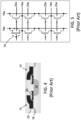
- the memory cell is shown in Fig. 2 .
- Each memory cell 10 includes source and drain regions 14/16 formed in a semiconductor substrate 12, with a channel region 18 there between.
- a floating gate 20 is formed over and insulated from (and controls the conductivity of) a first portion of the channel region 18, and over a portion of the drain region 16.
- a control gate 22 (i.e., a second, channel controlling gate) has a first portion 22b that is disposed over and insulated from (and controls the conductivity of) a second portion of the channel region 18, and a second portion 22c that extends up and over the floating gate 20.
- the floating gate 20 and control gate 22 are insulated from the substrate 12 by a gate oxide 26.
- the memory cell is erased (where electrons are removed from the floating gate) by placing a high positive voltage on the control gate 22, which causes electrons on the floating gate 20 to tunnel through the intermediate insulation 24 from the floating gate 20 to the control gate 22 via Fowler-Nordheim tunneling.
- the memory cell is programmed (where electrons are placed on the floating gate) by placing a positive voltage on the control gate 22, and a positive voltage on the drain 16. Electron current will flow from the source 14 towards the drain 16. The electrons will accelerate and become heated when they reach the gap between the control gate 22 and the floating gate 20. Some of the heated electrons will be injected through the gate oxide 26 onto the floating gate 20 due to the attractive electrostatic force from the floating gate 20.
- the memory cell is read by placing positive read voltages on the drain 16 and control gate 22 (which turns on the channel region under the control gate). If the floating gate 20 is positively charged (i.e. erased of electrons and positively coupled to the drain 16), then the portion of the channel region under the floating gate 20 is turned on as well, and current will flow across the channel region 18, which is sensed as the erased or "1" state. If the floating gate 20 is negatively charged (i.e. programmed with electrons), then the portion of the channel region under the floating gate 20 is mostly or entirely turned off, and current will not flow (or there will be little flow) across the channel region 18, which is sensed as the programmed or "0" state.
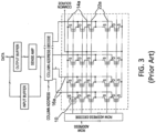
- the architecture of the memory array is shown in Fig. 3 .
- the memory cells 10 are arranged in rows and columns. In each column, the memory cells are arranged end to end in mirror fashion, so that they are formed as pairs of memory cells each sharing a common source region 14 (S), and each adjacent set of memory cell pairs sharing a common drain region 16 (D). All the source regions 14 for any given row of memory cells are electrically connected together by a source line 14a. All the drain regions 16 for any given column of memory cells are electrically connected together by a bit line 16a. All the control gates 22 for any given row of memory cells are electrically connected together by a control gate line 22a.
- memory cell erasure is performed row by row (each row of memory cells is erased together, by the application of a high voltage on the control gate line 22a). If a particular memory cell is to be erased, all the memory cells in the same row are also erased.
- Fig. 5 best illustrates the corresponding memory cell architecture, including the memory cells 10, the source lines 14a, the bit lines 16a, and the control gate lines 22a.
- memory cells 10 of the same row share the same source line 14a and the same control gate line 22a, while the drain regions of all cells of the same column are electrically connected to the same bit line 16a.
- the array design is optimized for digital applications, and permits individual programming of the selected cells, e.g., by applying 1.6 V and 7.6 V to the selected control gate line 22a and source line 14a, respectively, and grounding the selected bit line 16a.
- Disturbing the non-selected memory cell in the same pair is avoided by applying a voltage greater than 2 volts on the unselected bit lines 16a and grounding the remaining lines.
- the memory cells 10 cannot be erased individually because the process responsible for erasure (the Fowler-Nordheim tunneling of electrons from the floating gate 20 to the control gate 22) is only weakly affected by the drain voltage (i.e., the only voltage which may be different for two adjacent cells in the row direction sharing the same source line 14a).
- split gate memory cells having more than two gates are also known.
- memory cells have source region 14, drain region 16, floating gate 20 over a first portion of channel region 18, a select gate 28 (i.e., a second, channel controlling gate) over a second portion of the channel region 18, a control gate 22 over the floating gate 20, and an erase gate 30 over the source region 14 are known, as shown in Fig. 6 (see for example U.S. Patent 6,747,310 ).
- all gates are non-floating gates except floating gate 20, meaning that they are electrically connected or connectable to a voltage source. Programming is shown by heated electrons from the channel region 18 injecting themselves onto the floating gate 20. Erasing is shown by electrons tunneling from the floating gate 20 to the erase gate 30.
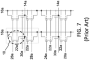
- each horizontal select gate line 28a electrically connects together all the select gates 28 for that row of memory cells.
- Each horizontal control gate line 22a electrically connects together all the control gates 22 for that row of memory cells.
- Each horizontal source line 14a electrically connects together all the source regions 14 for two rows of memory cells that share the source regions 14.
- Each bit line 16a electrically connects together all the drain regions 16 for that column of memory cells.
- Each erase gate line 30a electrically connects together all the erase gates 30 for two rows of memory cells that share the erase gate 30.
- individual memory cells can be independently programmed and read. However, there is no way to erase cells individually.
- Erasing is performed by placing a high positive voltage on the erase gate line 30a, which results in the simultaneous erasing of both rows of the memory cells that share the same erase gate line 30a.
- Exemplary operating voltages can include those in Table 1 below (in this embodiment, select gate lines 28a can be referred to as word lines WL): Table 1 WL BL SL CG EG Sel. Unsel. Sel. Unsel. Sel. Unsel. Sel. Unsel. Sel. Unsel. Sel. Unsel. Sel. Unsel. Unsel. Unsel. Unsel. Unsel. Sel. Unsel. Unsel. Unsel. Unsel. Unsel. Unsel. Unsel. Unsel. Unsel. Unsel. Unsel. Unsel. Unsel. Unsel. Unsel. Unsel. Unsel. Unsel. Unsel. Unsel. Unsel. Unsel. Unsel. Unsel. Unsel. Unsel. Unsel. Unsel. Unsel. Unsel. Unsel. Unsel. Unsel. Unsel. Unsel. Unsel. Unsel
- the lines are reconfigured so that each memory cell can be individually programmed, erased and read without adversely affecting the memory state of other memory cells in the array, as further explained below.
- continuous (analog) programming of the memory cells is provided. Specifically, the memory state (i.e. charge on the floating gate) of each memory cells in the array can be continuously changed from a fully erased state to a fully programmed state, and vice versa, independently and with minimal disturbance of other memory cells.
- An activation function P1 (pooling) is applied before going from C1 to S1, which pools values from consecutive, non-overlapping 2x2 regions in each feature map.
- the purpose of the pooling stage is to average out the nearby location (or a max function can also be used), to reduce the dependence of the edge location for example and to reduce the data size before going to the next stage.
- S1 there are 16 15x15 feature maps (i.e., sixteen different arrays of 15x15 pixels each).
- the synapses and associated neurons in CB2 going from S1 to C2 scan maps in S1 with 4x4 filters, with a filter shift of 1 pixel.
- At C2 there are 22 12x12 feature maps.
- Fig. 15 illustrates an array of four-gate memory cells (i.e., such as that shown in Fig. 6 ) arranged as a drain summing matrix multiplier.
- the various gate and region lines for the array of Fig. 15 are the same as that in Fig. 7 (with the same element numbers for corresponding structure), except that the erase gate lines 30a run vertically instead of horizontally (i.e., each erase gate line 30a connects together all the erase gates 30 for that column of memory cells) so that each memory cell 10 can be independently programmed, erased and read.
- the array acts as a drain summing matrix multiplier.
- the matrix inputs are Vin0... Vin7 and are placed on select gate lines 28a.
- each memory cell acts as a single synapse having a weight value expressed as output current Iout dictated by the sum of the weight values stored in the memory cell (or pair of memory cells) in that column.
- the output of any given synapse is in the form of current. Therefore, each subsequent VMM stage after the first stage preferably includes circuitry for converting incoming currents from the previous VMM stage into voltages to be used as the input voltages Vin.
- Fig. 16 illustrates an example of such current-to-voltage conversion circuitry, which is a modified row of memory cells that log converts the incoming currents Iin0 ...IinN into the input voltages Vin0..VinN.
- Vg k * Vt * log Ids / wp * Io
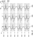
- Figs. 17 and 18 illustrate another configuration of an array of four-gate memory cells (i.e., such as that shown in Fig. 6 ) arranged as a drain summing matrix multiplier.
- the lines for the array of Figs. 17 and 18 are the same as that in the array of Figs. 15 and 16 , except that the source lines 14a run vertically instead of horizontally (i.e., each source line 14a connects together all the source regions 14 for that column of memory cells) and erase gate lines 30a run horizontally instead of vertically (i.e., each erase gate line 30a connects together all the erase gates 30 for that row of memory cell pairs), so that each memory cell can be independently programmed, erased and read.
- the matrix inputs VinO... VinN remain on select gate lines 28a, and the matrix outputs Iout0... IoutN remain on the bit lines 16a.
- Fig. 19 illustrates another configuration of an array of four-gate memory cells (i.e., such as that shown in Fig. 6 ) arranged as a gate coupling/source summing matrix multiplier.
- the lines for the array of Fig. 19 are the same as that in Figs. 15 and 16 , except that the select gate lines 28a run vertically and there are two of them for each column of memory cells.
- each column of memory cells include two select gate lines: a first select gate line 28a1 connecting together all the select gates 28 of the odd row memory cells, and a second select gate line 28a2 connecting together all the select gates 28 of the even row memory cells.
- the circuits at the top and bottom of Fig. 19 serve to log convert the input currents Iin0 ... IinN into the input voltages Vin0..VinN.
- the matrix inputs shown in this figure are VinO... Vin5 and are placed on the select gate lines 28a1 and 28a2. Specifically, input Vin0 is placed on the select line 28a1 for the odd cells in column 1. Vin1 is placed on the select gate line 28a2 for the even cells in column 1. Vin2 is placed on the select gate line 28a1 for the odd cells in column 2. Vin3 is placed on the select gate line 28a2 for the even cells in column 2, and so on.
- the matrix outputs Iout0... Iout3 are provided on the source lines 14a.
- the bit lines 16a are biased at fixed bias voltage VBLrd.
- Each output Iout is a sum of the cell current I times the weight W stored in the cell, for all the cells in that row of memory cells. Therefore, for this architecture, each row of memory cells acts as a single synapse having a weight value expressed as output current Iout dictated by the sum of the weight values stored in the memory cells in that row.
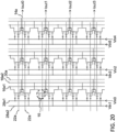
- Fig. 20 illustrates another configuration of an array of four-gate memory cells (i.e., such as that shown in Fig. 6 ) arranged as a gate coupling/source summing matrix multiplier.
- the lines for the array of Fig. 20 are the same as that in Fig. 19 , except that bit lines 16 run vertically and there are two of them for each column of memory cells.
- each column of memory cells include two bit lines: a first bit line 16a1 connecting together all the drain regions of the adjacent twin memory cells (two memory cells sharing the same bit line contact), and a second bit line 16a2 connecting together all the drain regions of the next adjacent twin memory cells.
- the matrix inputs Vin0... VinN remain on select gate lines 28a1 and 28a2, and the matrix outputs Iout0...
- the set of all the first bit lines 16a1 are biased at a bias level, e.g., 1.2v, and the set of all the second bit lines 16a2 are biased at another bias level, e.g., 0v.
- the source lines 14a are biased at a virtual bias level, e.g., 0.6v. For each pair of memory cells sharing a common source line 14a, the output current will be a differential output of the top cell minus the bottom cell.
- Fig. 21 illustrates another configuration of an array of four-gate memory cells (i.e., such as that shown in Fig. 6 ) arranged as a gate coupling/source summing matrix multiplier.
- the lines for the array of Fig. 21 are the same as that in Fig. 20 , except that the erase gates 30a run horizontally, and the control gate lines 22a run vertically and there are two of them for each column of memory cells.
- each column of memory cells include two control gate lines: a first control gate line 22a1 connecting together all the control gates 22a of the odd row memory cells, and a second control gate line 22a2 connecting together all the control gates 22a of the even row memory cells.
- the matrix inputs VinO... VinN remain on select gate lines 28a1 and 28a2, and the matrix outputs Iout0... IoutN remain on the source lines 14a.
- Fig. 22 illustrates another configuration of an array of four-gate memory cells (i.e., such as that shown in Fig. 6 ) arranged as a source summing matrix multiplier.
- the lines and inputs for the array of Fig. 22 are the same as that in Fig. 17 . However, instead of the outputs being provided on the bit lines 16a, they are provided on the source lines 14a.
- the matrix inputs Vin0... VinN remain on select gate lines 28a.
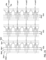
- Fig. 23 illustrates a configuration of an array of two-gate memory cells (i.e., such as that shown in Fig. 1 ) arranged as a drain summing matrix multiplier.
- the lines for the array of Fig. 23 are the same as that in Fig. 5 , except that the horizontal source lines 14a have been replaced with vertical source lines 14a. Specifically, each source line 14a is connected to all the source regions in that column of memory cells.
- the matrix inputs VinO... VinN are placed on the control gate lines 22a.
- the matrix outputs Iout0... IoutN are produced on the bit lines 16a.
- Each output Iout is a sum of the cell current I times the weight W stored in the cell, for all the cells in the column.
- Each column of memory cells acts as a single synapse having a weight value expressed as output current Iout dictated by the sum of the weight values stored in the memory cells for that column.
- Fig. 24 illustrates a configuration of an array of two-gate memory cells (i.e., such as that shown in Fig. 1 ) arranged as a source summing matrix multiplier.
- the lines for the array of Fig. 24 are the same as that in Fig. 5 , except that the control gate lines 22a run vertically and there are two of them for each column of memory cells.
- each column of memory cells include two control gate lines: a first control gate line 22a1 connecting together all the control gates 22a of the odd row memory cells, and a second control gate line 22a2 connecting together all the control gates 22a of the even row memory cells.
- the matrix inputs for this configuration are Vin0... VinN and are placed on the control gate lines 22a1 and 22a2. Specifically, input VinO is placed on control gate line 22a1 for the odd row cells in column 1. Vin1 is placed on the control gate line 22a2 for the even row cells in column 1. Vin2 is placed on the control gate line 22a1 for the odd row cells in column 2. Vin3 is placed on the control gate line 22a2 for the even row cells in column 2, and so on.
- the matrix outputs Iout0... IoutN are produced on the source lines 14a. For each pair of memory cells sharing a common source line 14a, the output current will be a differential output of the top cell minus the bottom cell. Therefore, for this architecture, each row of paired memory cells acts as a single synapse having a weight value expressed as output current Iout which is the sum of differential outputs dictated by the weight values stored in the memory cells in that row of paired memory cells.
- Exemplary operational voltages for the embodiments of Figs. 15-16 , 19 and 20 include: EG WL CG BL SL sel unsel sel unsel sel unsel sel unsel sel unsel Erase VEGerase gnd gnd gnd gnd VCGerinhibit gnd gnd gnd gnd Program VEGprg/ gnd gnd VWLprg gnd VCGprg gnd Iprog VBLprginh VSprg gnd Read gnd gnd VWLrd gnd VCGrd gnd VBLrd gnd VSrd float/ gnd
- Exemplary operational voltages for the embodiments of Figs. 17-18 and 22 include: EG WL CG BL SL sel unsel sel unsel sel unsel - shared EG unsel sel unsel sel unsel Erase VEGerase gnd gnd gnd gnd VCGerinh gnd gnd VBLerinh/ gnd VSLerinh gnd Program VEGprg/ gnd gnd VWLprg gnd VCGprg/ gnd gnd gnd Iprog VBLprginh VSprg gnd Read gnd gnd VWLrd gnd VCGrd gnd gnd VBLrd gnd VSrd float/gnd
- Approximate numerical values include: VEGerase 7-10v VSLerinh 3.5-6v VCGerinh 3.5-7v VBLerinh 1-2.5v VEGprg 4-6v VWLprg 0.8-1.2v VCGprg 6-10v VBLprginh 1-2.5v Iprog 0.2-1 ⁇ a VSprg 3-5V VWLrd 0.4-2.0V VCGrd 1-2.5V VBLrd 1-2V VSrd 0-0.6V
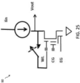
- Fig. 26 illustrates an exemplary voltage to current log converter 52 for use with the present invention.
- the memory is biased in a weak inversion region.
- Fig. 27 illustrates a Gnd-referred current summer 54 for use with the present invention.
- Fig. 28 below illustrates a Vdd-referred current summer 56 for use with the present invention.
- Examples of the load include a diode, a non-volatile memory cell, and a resistor.
- the above described memory array configurations implement a feed-forward classification-engine.
- the training is completed by storing "weight" values in the memory cells (creating a synapse array), which means subthreshold-slope-factors of the individual cells have been modified.
- the neurons are implemented by summing the outputs of synapse and firing or not firing depending on the neuron threshold (i.e., making a decision).
- Step 2 Apply the generated bias voltage VBE to the word line (in subthreshold region).
- each of the cells could be tied together in the read mode to sum up the values of each synapse in the array or sector of the array.
- I DRAIN Once I DRAIN has been summed up, it can be fed into a current comparator, and output a "logic" 0 or 1 depending on the comparison for a single perception neural network.
- One perception one sector is described above.
- the output from each perception can be fed to the next set of sectors for multiple perceptions.
- a set of inputs needs to be multiplied with certain weights to produce a desired result for a hidden layer or output layer.
- the first row of six pixels in the filter is provided to the first 6 of the inputs to the memory array of N 2 inputs.
- the second row of six pixels in the filter is provided to the first 6 of the inputs in the second N inputs of the N 2 inputs, and so on.
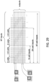
- This is represented in the first row of the diagram in Fig. 29 , where the dots represent the weights stored in the memory array for multiplication by the inputs as set forth above.
- the filter is shifted to the right by two pixels, and the first row of six pixels in the shifted filter is provided to the third through the eighth inputs of the first N inputs, the second row of six pixels is provided to the third through the eight inputs of the second N inputs, and so on.
- Each set of horizontally shifted scans can be represented by trapezoidal shapes showing which of the N 2 memory array inputs are provided with data for multiplication.
- a scan of NxN image array using a shift of two pixels between scans, and a filter size of 6x6, requires N 2 inputs and ((N-4)/2)) 2 rows.
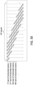
- Fig. 30 graphically shows the trapezoidal shapes indicating how the weights in the memory array are stored for the filter scan. Each row of shaded areas represents weights being applied to the inputs during one set of the horizontal scans.
- the arrows indicate linear input lines of the memory array (e.g., the input lines 28a in Fig. 15 that receive the input data extend all the way across the memory array in a linear manner, each one always accessing the same row of memory cells; in the case of the array of Fig. 19 , each of the input lines always access the same column of memory cells).
- the white areas indicate where no data is being supplied to the inputs. Therefore, the white areas are indicative of inefficient use of the memory cell array.
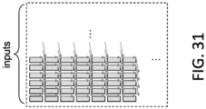
- Efficiency can be increased, and the total number of inputs reduced, by reconfiguring the memory arrays as shown in Fig. 31 .
- the input lines of the memory array are shifted periodically to another row or column, thus reducing the unused portions of the array, and therefore reducing the number of repeated input lines over the array needed to perform the scan.
- the arrows indicate that each input line periodically shifts over by two rows or two columns, transforming the widely spaced apart memory cell utilization trapezoidal shapes to closely spaced memory cell utilization rectangular shapes. While extra space between memory cell portions are needed for wire bundles to implement this shift, the number of inputs needed in the memory cell array is greatly reduced (only 5n+6).
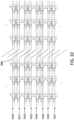
- Fig. 32 illustrates the array of Fig. 15 , but with periodic shifts of two rows for lines 28a used as the input lines.
- the periodic shift in rows for the input lines can be similarly implemented in the arrays of Figs. 17 , 22 and 23 .
- Fig. 33 illustrates the array of Fig. 20 , but with periodic shifts of two columns for lines 28a1 and 28a2 used as the input lines.
- the periodic shift in column for the input lines can be similarly implemented in the arrays of Figs. 19 , 21 and 24 .
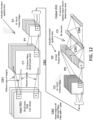
- the two key parameters for the above described convoluted neural networks are the filter size (i.e., 2x2, 3x3, 4x4, 5x5, etc.) and the filter stride (the number of pixels the filter moves in the x and y direction in any given step). See for example discussion above with respect to Figs. 12 and 29-31 .
- These two key parameters are implemented by design of the flash memory array. Photolithography masks used to fabricate the flash memory array dictate the memory array configuration, design and operation. Once the masks are made, changes to the memory array configuration and operation are not practically possible.
- the solution to this issue is to build the memory array at one end of the filter size and filter stride ranges, and provide a way to program the memory array with filter size and filter stride during the final stages of product manufacture (i.e. during final test sort). This will allow the same masks to be used to make memory array neural network devices with different filter sizes and filter strides.
- This programming can be implemented by disabling certain memory cells to selectively shut them down. Disabling a memory cell can be implemented in one or more ways. The most reliable technique for disabling a memory cell is disconnecting the memory cell from the line on which the outputs of other cells are collected. For example, if the cell outputs are collected (i.e., summed) on the bit lines, then the memory cell's drain region is disconnected from bit line.
- the bit line contact is the vertical connector that connects the memory cell's drain to the bit line. Etching away that contact means that there is no electrical connection between the memory cell's drain to any bit line. If the cell outputs are collected on the source lines, then the memory cell's source region is disconnected from the source line, however in some implementations, that may be more difficult or not feasible. Alternately, a fuse can be placed between the memory cell drain and the bit line, or between the source and source line, for each cell. The fuse for any enabled memory cell is in a conductive state. The fuse for any disabled memory cell is in a nonconductive state (i.e.
- Fig. 34A showing the bit line contact 60 between the bit line 16a and drain 16 removed (from the right hand cell)
- Fig. 34B showing the source line contact 62 between the source 14 and a raised source line 14a removed
- Fig. 34C showing fuses 64 on the bit line contacts 60
- Fig. 34D showing a fuse 64 on the source line contact 62.
- the fuse could instead constitute the entire connection between the source/drain and the source/bit line.
- the removal or fusing of the bit line contact or the source line contact can be similarly implemented with a memory array utilizing the four gate cell structure of Fig. 6 .
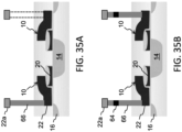
- a second technique for disabling a memory cell is to disconnect one or more of the memory cell's gates from the associated gate line(s). For example, a photolithography and etch step to remove a gate line contact can be performed. Alternately, a fuse can be placed between the memory cell gate and the gate line, which is blown open to disconnect the two. This would prevent the memory cell from being erased and then later turned on. See Fig. 35A showing the gate line contact 66 removed (from the right hand cell), and Fig. 35B showing fuses 64 on the gate line contacts 66. It should be noted, however, that the fuse could instead constitute the entire connection between the gate and the gate line.
- the removal or fusing of the gate line contact can be similarly implemented with a memory array utilizing the four gate cell structure of Fig. 6 , where one or more of the select, control and erase gates can be disconnected from their associated gate line(s). Because the disconnected gate will be floating, some leakage through the cell may occur. Therefore, the reliability of this second technique can be enhanced by programming the floating gate with enough electrons to prevent such leakage during subsequent operations involving the other cells which were not disabled. This programming can occur before the gate line contact is removed and/or the fuse thereon blown. It is also possible to combine the first and second techniques for disabling selected memory cells.
- any erroneous leakage or voltage contribution by the memory cells in the array not being used for the scan can contribute to error.
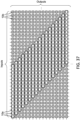
- the memory cells in each row not being used for the scan are disabled. This is shown in Fig. 37 , where memory cells 10a used for the scan remain enabled, and memory cells 10b not used for the scan (marked with "X") are disabled using one or both of the techniques described above. The disabled memory cells 10b are prevented from contributing to the output of the enabled cells 10a in the same row.
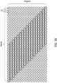
- Fig. 38 illustrates the same configuration as that in Fig. 37 , except that the stride of 1 is changed to a stride of 2.
- Fig. 39 illustrates the same configuration as that in Fig. 37 , except the scan is for a 3x3 filter, involving 9 enabled cells in each row of the array.
- Fig. 40 illustrates the memory cells involved in the beginning of a scan for a 3x3 filter of stride 1, in or similar to one of the above described array configurations where the input signals are placed on horizontally extending lines (e.g. select gate lines 28a, control gate lines 22a, etc.) and the output signals are generated on vertically extending lines (e.g. source lines 14a, bit lines 16a, etc.).
- horizontally extending lines e.g. select gate lines 28a, control gate lines 22a, etc.
- vertically extending lines e.g. source lines 14a, bit lines 16a, etc.
- the same memory array architecture can be used to perform a scan of different filter size, formed by the same set of initial masks and processing steps. It is only later on in the manufacturing process, or even after the manufacturing process, that certain memory cells are disabled to customize the performance for a certain filter size, and prevent the disabled cells not used by a scan of that filter size from contributing to the output signals from the enabled memory cells.
- the term “adjacent” includes “directly adjacent” (no intermediate materials, elements or space disposed therebetween) and “indirectly adjacent” (intermediate materials, elements or space disposed there between), “mounted to” includes “directly mounted to” (no intermediate materials, elements or space disposed there between) and “indirectly mounted to” (intermediate materials, elements or spaced disposed there between), and “electrically coupled” includes “directly electrically coupled to” (no intermediate materials or elements there between that electrically connect the elements together) and “indirectly electrically coupled to” (intermediate materials or elements there between that electrically connect the elements together).
- forming an element "over a substrate” can include forming the element directly on the substrate with no intermediate materials/elements therebetween, as well as forming the element indirectly on the substrate with one or more intermediate materials/elements there between.
Landscapes
- Engineering & Computer Science (AREA)
- Physics & Mathematics (AREA)
- Theoretical Computer Science (AREA)
- Health & Medical Sciences (AREA)
- Life Sciences & Earth Sciences (AREA)
- Biomedical Technology (AREA)
- Biophysics (AREA)
- Microelectronics & Electronic Packaging (AREA)
- Molecular Biology (AREA)
- General Health & Medical Sciences (AREA)
- Software Systems (AREA)
- Data Mining & Analysis (AREA)
- Computing Systems (AREA)
- General Engineering & Computer Science (AREA)
- General Physics & Mathematics (AREA)
- Mathematical Physics (AREA)
- Evolutionary Computation (AREA)
- Computational Linguistics (AREA)
- Artificial Intelligence (AREA)
- Neurology (AREA)
- Non-Volatile Memory (AREA)
- Semiconductor Memories (AREA)
- Metal-Oxide And Bipolar Metal-Oxide Semiconductor Integrated Circuits (AREA)
Claims (3)
- Speicherarray, umfassend:eine Vielzahl von Speicherzellen (10), die in Reihen und Spalten angeordnet sind, wobei jede der Speicherzellen einschließt:voneinander beabstandete Source- und Drain-Bereiche (14, 16), die in einem Halbleitersubstrat (12) mit einem Kanalbereich (18) ausgebildet sind, der sich dazwischen erstreckt,ein Floating-Gate (20), das über einem ersten Abschnitt des Kanalbereichs eingerichtet und von diesem isoliert ist, undein zweites Gate, das über einem zweiten Abschnitt des Kanalbereichs eingerichtet und von diesem isoliert ist;eine Vielzahl von Gate-Leitungen (22a), die sich jeweils entlang einer entsprechenden der Reihen oder Spalten erstrecken, wobei für jede der Gate-Leitungen und ihrer entsprechenden Reihe oder Spalte die Gate-Leitung mit den zweiten Gates einer ersten Gruppe von einer oder mehreren der Speicherzellen in der entsprechenden Reihe oder Spalte elektrisch verbunden ist und von den zweiten Gates einer zweiten Gruppe von einer oder mehreren der Speicherzellen in der entsprechenden Reihe oder Spalte elektrisch isoliert ist;eine Vielzahl von Bit-Leitungen (16a), die jeweils mit den Drain-Bereichen (16) von mindestens einigen der Speicherzellen in einer entsprechenden der Spalten elektrisch verbunden sind;eine Vielzahl von Source-Leitungen (14a), die jeweils mit den Source-Bereichen (14) von mindestens einigen der Speicherzellen in einer entsprechenden der Spalten oder in einer entsprechenden der Reihen elektrisch verbunden sind;wobei:eine erste der Reihen eine erste Vielzahl der Speicherzellen (10) einschließt, die in einer Reihenrichtung angrenzend aneinander positioniert sind, wobei das zweite Gate für jede der ersten Vielzahl von Speicherzellen mit einer der Gate-Leitungen (22a) elektrisch verbunden ist;die erste der Reihen eine zweite Vielzahl der Speicherzellen einschließt, die die erste Vielzahl der Speicherzellen in der Reihenrichtung umgeben, wobei das zweite Gate für jede der zweiten Vielzahl von Speicherzellen nicht mit einer beliebigen der Gate-Leitungen elektrisch verbunden ist;eine zweite der Reihen angrenzend an die erste der Reihen ist und eine dritte Vielzahl der Speicherzellen einschließt, die in der Reihenrichtung angrenzend aneinander positioniert sind, wobei das zweite Gate für jede der dritten Vielzahl von Speicherzellen mit einer der Gate-Leitungen elektrisch verbunden ist;die zweite der Reihen eine vierte Vielzahl der Speicherzellen einschließt, die die dritte Vielzahl der Speicherzellen in der Reihenrichtung umgeben, wobei das zweite Gate für jede der vierten Vielzahl von Speicherzellen nicht mit einer beliebigen der Gate-Leitungen elektrisch verbunden ist;sich eine der ersten Vielzahl von Speicherzellen und eine der vierten Vielzahl von Speicherzellen in derselben Spalte befinden.
- Speicherarray nach Anspruch 1, wobei für jede der Gate-Leitungen (22a) und ihrer entsprechenden Reihe oder Spalte das Speicherarray ferner umfasst:
eine Vielzahl von Gate-Leitungskontakten, die jeweils das zweite Gate von einer der Speicherzellen (10) in der ersten Gruppe mit der Gate-Leitung elektrisch verbinden. - Speicherarray nach Anspruch 2, wobei für jede der Gate-Leitungen (22a) und ihrer entsprechenden Reihe oder Spalte jeder der Speicherzellen (10) in der zweiten Gruppe ein Gate-Leitungskontakt fehlt, der das zweite Gate mit der Gate-Leitung elektrisch verbindet.
Applications Claiming Priority (4)
| Application Number | Priority Date | Filing Date | Title |
|---|---|---|---|
| US201762558984P | 2017-09-15 | 2017-09-15 | |
| US16/107,282 US10580492B2 (en) | 2017-09-15 | 2018-08-21 | System and method for implementing configurable convoluted neural networks with flash memories |
| EP18856570.9A EP3665722B1 (de) | 2017-09-15 | 2018-08-22 | System und verfahren zur implementierung konfigurierbarer gefalteter neuronaler netze mit flash-speichern |
| PCT/US2018/047438 WO2019055182A1 (en) | 2017-09-15 | 2018-08-22 | SYSTEM AND METHOD FOR IMPLEMENTING CONVOLUTE NEURAL NETWORKS CONFIGURABLE WITH FLASH MEMOIRES |
Related Parent Applications (2)
| Application Number | Title | Priority Date | Filing Date |
|---|---|---|---|
| EP18856570.9A Division EP3665722B1 (de) | 2017-09-15 | 2018-08-22 | System und verfahren zur implementierung konfigurierbarer gefalteter neuronaler netze mit flash-speichern |
| EP18856570.9A Division-Into EP3665722B1 (de) | 2017-09-15 | 2018-08-22 | System und verfahren zur implementierung konfigurierbarer gefalteter neuronaler netze mit flash-speichern |
Publications (3)
| Publication Number | Publication Date |
|---|---|
| EP4235513A2 EP4235513A2 (de) | 2023-08-30 |
| EP4235513A3 EP4235513A3 (de) | 2023-11-01 |
| EP4235513B1 true EP4235513B1 (de) | 2025-03-19 |
Family
ID=65721171
Family Applications (3)
| Application Number | Title | Priority Date | Filing Date |
|---|---|---|---|
| EP18856570.9A Active EP3665722B1 (de) | 2017-09-15 | 2018-08-22 | System und verfahren zur implementierung konfigurierbarer gefalteter neuronaler netze mit flash-speichern |
| EP23180121.8A Active EP4235513B1 (de) | 2017-09-15 | 2018-08-22 | System und verfahren zur implementierung konfigurierbarer gefalteter neuronaler netze mit flash-speichern |
| EP23179955.2A Active EP4235512B1 (de) | 2017-09-15 | 2018-08-22 | System und verfahren zur implementierung konfigurierbarer gefalteter neuronaler netze mit flash-speichern |
Family Applications Before (1)
| Application Number | Title | Priority Date | Filing Date |
|---|---|---|---|
| EP18856570.9A Active EP3665722B1 (de) | 2017-09-15 | 2018-08-22 | System und verfahren zur implementierung konfigurierbarer gefalteter neuronaler netze mit flash-speichern |
Family Applications After (1)
| Application Number | Title | Priority Date | Filing Date |
|---|---|---|---|
| EP23179955.2A Active EP4235512B1 (de) | 2017-09-15 | 2018-08-22 | System und verfahren zur implementierung konfigurierbarer gefalteter neuronaler netze mit flash-speichern |
Country Status (7)
| Country | Link |
|---|---|
| US (1) | US10580492B2 (de) |
| EP (3) | EP3665722B1 (de) |
| JP (1) | JP7250776B2 (de) |
| KR (1) | KR102307675B1 (de) |
| CN (1) | CN111095553B (de) |
| TW (1) | TWI693610B (de) |
| WO (1) | WO2019055182A1 (de) |
Families Citing this family (24)
| Publication number | Priority date | Publication date | Assignee | Title |
|---|---|---|---|---|
| KR102182583B1 (ko) | 2016-05-17 | 2020-11-24 | 실리콘 스토리지 테크놀로지 인크 | 비휘발성 메모리 어레이를 사용하는 딥러닝 신경망 분류기 |
| US10803943B2 (en) | 2017-11-29 | 2020-10-13 | Silicon Storage Technology, Inc. | Neural network classifier using array of four-gate non-volatile memory cells |
| US11636325B2 (en) | 2018-10-24 | 2023-04-25 | Macronix International Co., Ltd. | In-memory data pooling for machine learning |
| US11562229B2 (en) * | 2018-11-30 | 2023-01-24 | Macronix International Co., Ltd. | Convolution accelerator using in-memory computation |
| US11934480B2 (en) | 2018-12-18 | 2024-03-19 | Macronix International Co., Ltd. | NAND block architecture for in-memory multiply-and-accumulate operations |
| US11500442B2 (en) | 2019-01-18 | 2022-11-15 | Silicon Storage Technology, Inc. | System for converting neuron current into neuron current-based time pulses in an analog neural memory in a deep learning artificial neural network |
| US11270763B2 (en) | 2019-01-18 | 2022-03-08 | Silicon Storage Technology, Inc. | Neural network classifier using array of three-gate non-volatile memory cells |
| US11023559B2 (en) | 2019-01-25 | 2021-06-01 | Microsemi Soc Corp. | Apparatus and method for combining analog neural net with FPGA routing in a monolithic integrated circuit |
| US11586898B2 (en) * | 2019-01-29 | 2023-02-21 | Silicon Storage Technology, Inc. | Precision programming circuit for analog neural memory in deep learning artificial neural network |
| US11270771B2 (en) | 2019-01-29 | 2022-03-08 | Silicon Storage Technology, Inc. | Neural network classifier using array of stacked gate non-volatile memory cells |
| US11423979B2 (en) | 2019-04-29 | 2022-08-23 | Silicon Storage Technology, Inc. | Decoding system and physical layout for analog neural memory in deep learning artificial neural network |
| US12353503B2 (en) * | 2019-05-02 | 2025-07-08 | Silicon Storage Technology, Inc. | Output array neuron conversion and calibration for analog neural memory in deep learning artificial neural network |
| US11521658B2 (en) | 2019-06-25 | 2022-12-06 | Sandisk Technologies Llc | Binary weighted voltage encoding scheme for supporting multi-bit input precision |
| US11393546B2 (en) * | 2019-07-19 | 2022-07-19 | Silicon Storage Technology, Inc. | Testing circuitry and methods for analog neural memory in artificial neural network |
| US20210034953A1 (en) * | 2019-08-02 | 2021-02-04 | Applied Materials, Inc. | Reconfigurable finfet-based artificial neuron and synapse devices |
| US11507816B2 (en) | 2019-09-19 | 2022-11-22 | Silicon Storage Technology, Inc. | Precision tuning for the programming of analog neural memory in a deep learning artificial neural network |
| EP3963514A1 (de) * | 2020-06-25 | 2022-03-09 | PolyN Technology Limited | Analoge hardware-realisierung neuronaler netze |
| KR102514932B1 (ko) * | 2021-04-16 | 2023-03-29 | 한국과학기술원 | 기계 학습용 아날로그 내적 연산기, 이를 이용한 기계 학습 프로세서 및 학습 방법 |
| KR102590585B1 (ko) * | 2021-08-10 | 2023-10-16 | 고려대학교 산학협력단 | 3 전극 대각 멤트랜지스터 시스템, 이를 이용한 컨볼루션 네트워크 연산 장치 및 방법 |
| US12299597B2 (en) | 2021-08-27 | 2025-05-13 | Macronix International Co., Ltd. | Reconfigurable AI system |
| US12321603B2 (en) | 2023-02-22 | 2025-06-03 | Macronix International Co., Ltd. | High bandwidth non-volatile memory for AI inference system |
| US12536404B2 (en) | 2023-02-22 | 2026-01-27 | Macronix International Co., Ltd. | Data optimization for high bandwidth (HBW) NVM AI inference system |
| US12585931B2 (en) * | 2023-05-04 | 2026-03-24 | Macronix International Co., Ltd. | 3D hybrid bonding 3D memory devices with NPU/CPU for AI inference application |
| US12417170B2 (en) | 2023-05-10 | 2025-09-16 | Macronix International Co., Ltd. | Computing system and method of operation thereof |
Family Cites Families (37)
| Publication number | Priority date | Publication date | Assignee | Title |
|---|---|---|---|---|
| US5029130A (en) | 1990-01-22 | 1991-07-02 | Silicon Storage Technology, Inc. | Single transistor non-valatile electrically alterable semiconductor memory device |
| US5146602A (en) | 1990-12-26 | 1992-09-08 | Intel Corporation | Method of increasing the accuracy of an analog neural network and the like |
| US5138576A (en) | 1991-11-06 | 1992-08-11 | Altera Corporation | Method and apparatus for erasing an array of electrically erasable EPROM cells |
| DE69319162T2 (de) | 1992-03-26 | 1999-03-25 | Hitachi Vlsi Engineering Corp., Kodaira, Tokio/Tokyo | Flash-Speicher |
| US5264734A (en) | 1992-05-19 | 1993-11-23 | Intel Corporation | Difference calculating neural network utilizing switched capacitors |
| US5256911A (en) | 1992-06-10 | 1993-10-26 | Intel Corporation | Neural network with multiplexed snyaptic processing |
| JP2835272B2 (ja) | 1993-12-21 | 1998-12-14 | 株式会社東芝 | 半導体記憶装置 |
| KR0151623B1 (ko) | 1994-12-07 | 1998-10-01 | 문정환 | 이이피롬 셀 및 그 제조방법 |
| US5554874A (en) | 1995-06-05 | 1996-09-10 | Quantum Effect Design, Inc. | Six-transistor cell with wide bit-line pitch, double words lines, and bit-line contact shared among four cells |
| US6222777B1 (en) | 1999-04-09 | 2001-04-24 | Sun Microsystems, Inc. | Output circuit for alternating multiple bit line per column memory architecture |
| US6563167B2 (en) | 2001-01-05 | 2003-05-13 | Silicon Storage Technology, Inc. | Semiconductor memory array of floating gate memory cells with floating gates having multiple sharp edges |
| US6563733B2 (en) * | 2001-05-24 | 2003-05-13 | Winbond Electronics Corporation | Memory array architectures based on a triple-polysilicon source-side injection non-volatile memory cell |
| US6747310B2 (en) | 2002-10-07 | 2004-06-08 | Actrans System Inc. | Flash memory cells with separated self-aligned select and erase gates, and process of fabrication |
| US6822910B2 (en) | 2002-12-29 | 2004-11-23 | Macronix International Co., Ltd. | Non-volatile memory and operating method thereof |
| TWI220560B (en) | 2003-10-27 | 2004-08-21 | Powerchip Semiconductor Corp | NAND flash memory cell architecture, NAND flash memory cell array, manufacturing method and operating method of the same |
| US7072215B2 (en) * | 2004-02-24 | 2006-07-04 | Taiwan Semiconductor Manufacturing Company | Array structure of two-transistor cells with merged floating gates for byte erase and re-write if disturbed algorithm |
| US7315056B2 (en) | 2004-06-07 | 2008-01-01 | Silicon Storage Technology, Inc. | Semiconductor memory array of floating gate memory cells with program/erase and select gates |
| US7381615B2 (en) * | 2004-11-23 | 2008-06-03 | Sandisk Corporation | Methods for self-aligned trench filling with grown dielectric for high coupling ratio in semiconductor devices |
| TWI270199B (en) | 2005-01-31 | 2007-01-01 | Powerchip Semiconductor Corp | Non-volatile memory and manufacturing method and operating method thereof |
| US7304890B2 (en) | 2005-12-13 | 2007-12-04 | Atmel Corporation | Double byte select high voltage line for EEPROM memory block |
| US7951669B2 (en) * | 2006-04-13 | 2011-05-31 | Sandisk Corporation | Methods of making flash memory cell arrays having dual control gates per memory cell charge storage element |
| TW200847430A (en) * | 2007-05-22 | 2008-12-01 | Chia-Hsing Chen | A MOSFET device and its operation method |
| JP2010267341A (ja) | 2009-05-15 | 2010-11-25 | Renesas Electronics Corp | 半導体装置 |
| US8909576B2 (en) | 2011-09-16 | 2014-12-09 | International Business Machines Corporation | Neuromorphic event-driven neural computing architecture in a scalable neural network |
| US8760955B2 (en) | 2011-10-21 | 2014-06-24 | Taiwan Semiconductor Manufacturing Company, Ltd. | Electrical fuse memory arrays |
| US9275748B2 (en) * | 2013-03-14 | 2016-03-01 | Silicon Storage Technology, Inc. | Low leakage, low threshold voltage, split-gate flash cell operation |
| US10095718B2 (en) | 2013-10-16 | 2018-10-09 | University Of Tennessee Research Foundation | Method and apparatus for constructing a dynamic adaptive neural network array (DANNA) |
| US9299798B2 (en) * | 2013-11-26 | 2016-03-29 | Globalfoundries Singapore Pte. Ltd. | Semiconductor device and methods for forming a semiconductor device |
| US20150213898A1 (en) | 2014-01-27 | 2015-07-30 | Silicon Storage Technololgy, Inc. | Byte Erasable Non-volatile Memory Architecture And Method Of Erasing Same |
| US9209031B2 (en) * | 2014-03-07 | 2015-12-08 | Sandisk Technologies Inc. | Metal replacement process for low resistance source contacts in 3D NAND |
| US9286982B2 (en) | 2014-08-08 | 2016-03-15 | Silicon Storage Technology, Inc. | Flash memory system with EEPROM functionality |
| US10312248B2 (en) | 2014-11-12 | 2019-06-04 | Silicon Storage Technology, Inc. | Virtual ground non-volatile memory array |
| CN105990367B (zh) | 2015-02-27 | 2019-03-12 | 硅存储技术公司 | 具有rom单元的非易失性存储器单元阵列 |
| KR102487526B1 (ko) * | 2015-11-06 | 2023-01-12 | 에스케이하이닉스 주식회사 | 반도체 장치 및 그 제조방법 |
| WO2017200850A1 (en) | 2016-05-17 | 2017-11-23 | Silicon Storage Technology, Inc. | Array of three-gate flash memory cells with individual memory cell read, program and erase |
| KR102182583B1 (ko) * | 2016-05-17 | 2020-11-24 | 실리콘 스토리지 테크놀로지 인크 | 비휘발성 메모리 어레이를 사용하는 딥러닝 신경망 분류기 |
| US10269440B2 (en) * | 2016-05-17 | 2019-04-23 | Silicon Storage Technology, Inc. | Flash memory array with individual memory cell read, program and erase |
-
2018
- 2018-08-21 US US16/107,282 patent/US10580492B2/en active Active
- 2018-08-22 KR KR1020207006596A patent/KR102307675B1/ko active Active
- 2018-08-22 EP EP18856570.9A patent/EP3665722B1/de active Active
- 2018-08-22 WO PCT/US2018/047438 patent/WO2019055182A1/en not_active Ceased
- 2018-08-22 JP JP2020515174A patent/JP7250776B2/ja active Active
- 2018-08-22 EP EP23180121.8A patent/EP4235513B1/de active Active
- 2018-08-22 EP EP23179955.2A patent/EP4235512B1/de active Active
- 2018-08-22 CN CN201880059542.2A patent/CN111095553B/zh active Active
- 2018-09-14 TW TW107132513A patent/TWI693610B/zh active
Also Published As
| Publication number | Publication date |
|---|---|
| TWI693610B (zh) | 2020-05-11 |
| EP4235512A2 (de) | 2023-08-30 |
| WO2019055182A1 (en) | 2019-03-21 |
| JP7250776B2 (ja) | 2023-04-03 |
| JP2020534686A (ja) | 2020-11-26 |
| CN111095553A (zh) | 2020-05-01 |
| KR102307675B1 (ko) | 2021-10-01 |
| EP4235513A2 (de) | 2023-08-30 |
| KR20200036924A (ko) | 2020-04-07 |
| EP3665722A4 (de) | 2021-10-27 |
| CN111095553B (zh) | 2023-09-01 |
| US20190088329A1 (en) | 2019-03-21 |
| EP4235512B1 (de) | 2025-03-19 |
| EP3665722A1 (de) | 2020-06-17 |
| US10580492B2 (en) | 2020-03-03 |
| EP4235513A3 (de) | 2023-11-01 |
| TW201921349A (zh) | 2019-06-01 |
| EP3665722B1 (de) | 2023-07-26 |
| EP4235512A3 (de) | 2023-11-01 |
Similar Documents
| Publication | Publication Date | Title |
|---|---|---|
| EP4235513B1 (de) | System und verfahren zur implementierung konfigurierbarer gefalteter neuronaler netze mit flash-speichern | |
| US12347484B2 (en) | Memory device of non-volatile memory cells | |
| EP3676840B1 (de) | Hochpräzise und hocheffiziente abstimmungsmechanismen und algorithmen für analoge neuromorphe speicher in künstlichen neuronalen netzen | |
| EP3459019B1 (de) | Tiefenlernender neuronaler netzwerkklassifizierer mit nichtflüchtiger speicheranordnung | |
| EP3918533B1 (de) | Klassifizierer basiert auf einem neuronalen netzwerk, mit einer anordnung von nichtflüchtigen speicherzellen mit gestapelten gates | |
| EP3912100B1 (de) | Klassifizierer basiert auf einem neuronalen netzwerk, das ein nicht-flüchtiges speicherzellennetzwerk mit zwei gates verwendet | |
| EP3918532B1 (de) | Klassifizierer basiert auf einem neuronalen netzwerk, das ein nicht-flüchtiges speicherzellennetzwerk mit vier gates verwendet |
Legal Events
| Date | Code | Title | Description |
|---|---|---|---|
| PUAI | Public reference made under article 153(3) epc to a published international application that has entered the european phase |
Free format text: ORIGINAL CODE: 0009012 |
|
| STAA | Information on the status of an ep patent application or granted ep patent |
Free format text: STATUS: THE APPLICATION HAS BEEN PUBLISHED |
|
| AC | Divisional application: reference to earlier application |
Ref document number: 3665722 Country of ref document: EP Kind code of ref document: P |
|
| AK | Designated contracting states |
Kind code of ref document: A2 Designated state(s): AL AT BE BG CH CY CZ DE DK EE ES FI FR GB GR HR HU IE IS IT LI LT LU LV MC MK MT NL NO PL PT RO RS SE SI SK SM TR |
|
| REG | Reference to a national code |
Ref country code: DE Ref legal event code: R079 Free format text: PREVIOUS MAIN CLASS: G06N0003065000 Ipc: G06N0003045000 Ref document number: 602018080397 Country of ref document: DE |
|
| PUAL | Search report despatched |
Free format text: ORIGINAL CODE: 0009013 |
|
| AK | Designated contracting states |
Kind code of ref document: A3 Designated state(s): AL AT BE BG CH CY CZ DE DK EE ES FI FR GB GR HR HU IE IS IT LI LT LU LV MC MK MT NL NO PL PT RO RS SE SI SK SM TR |
|
| RIC1 | Information provided on ipc code assigned before grant |
Ipc: G11C 16/24 20060101ALI20230922BHEP Ipc: G06N 3/063 20230101ALI20230922BHEP Ipc: G06N 3/04 20230101ALI20230922BHEP Ipc: G11C 7/10 20060101ALI20230922BHEP Ipc: G11C 5/02 20060101ALI20230922BHEP Ipc: G11C 16/04 20060101ALI20230922BHEP Ipc: H10B 41/30 20230101ALI20230922BHEP Ipc: G06N 3/065 20230101ALI20230922BHEP Ipc: G06N 3/048 20230101ALI20230922BHEP Ipc: G06N 3/045 20230101AFI20230922BHEP |
|
| STAA | Information on the status of an ep patent application or granted ep patent |
Free format text: STATUS: REQUEST FOR EXAMINATION WAS MADE |
|
| 17P | Request for examination filed |
Effective date: 20240429 |
|
| RBV | Designated contracting states (corrected) |
Designated state(s): AL AT BE BG CH CY CZ DE DK EE ES FI FR GB GR HR HU IE IS IT LI LT LU LV MC MK MT NL NO PL PT RO RS SE SI SK SM TR |
|
| GRAP | Despatch of communication of intention to grant a patent |
Free format text: ORIGINAL CODE: EPIDOSNIGR1 |
|
| STAA | Information on the status of an ep patent application or granted ep patent |
Free format text: STATUS: GRANT OF PATENT IS INTENDED |
|
| INTG | Intention to grant announced |
Effective date: 20241009 |
|
| RIN1 | Information on inventor provided before grant (corrected) |
Inventor name: DO, NHAN Inventor name: TIWARI, VIPIN |
|
| GRAS | Grant fee paid |
Free format text: ORIGINAL CODE: EPIDOSNIGR3 |
|
| GRAA | (expected) grant |
Free format text: ORIGINAL CODE: 0009210 |
|
| STAA | Information on the status of an ep patent application or granted ep patent |
Free format text: STATUS: THE PATENT HAS BEEN GRANTED |
|
| AC | Divisional application: reference to earlier application |
Ref document number: 3665722 Country of ref document: EP Kind code of ref document: P |
|
| AK | Designated contracting states |
Kind code of ref document: B1 Designated state(s): AL AT BE BG CH CY CZ DE DK EE ES FI FR GB GR HR HU IE IS IT LI LT LU LV MC MK MT NL NO PL PT RO RS SE SI SK SM TR |
|
| P01 | Opt-out of the competence of the unified patent court (upc) registered |
Free format text: CASE NUMBER: APP_6470/2025 Effective date: 20250207 |
|
| REG | Reference to a national code |
Ref country code: GB Ref legal event code: FG4D |
|
| REG | Reference to a national code |
Ref country code: CH Ref legal event code: EP |
|
| REG | Reference to a national code |
Ref country code: IE Ref legal event code: FG4D |
|
| REG | Reference to a national code |
Ref country code: DE Ref legal event code: R096 Ref document number: 602018080397 Country of ref document: DE |
|
| REG | Reference to a national code |
Ref country code: NL Ref legal event code: FP |
|
| PG25 | Lapsed in a contracting state [announced via postgrant information from national office to epo] |
Ref country code: RS Free format text: LAPSE BECAUSE OF FAILURE TO SUBMIT A TRANSLATION OF THE DESCRIPTION OR TO PAY THE FEE WITHIN THE PRESCRIBED TIME-LIMIT Effective date: 20250619 |
|
| PG25 | Lapsed in a contracting state [announced via postgrant information from national office to epo] |
Ref country code: FI Free format text: LAPSE BECAUSE OF FAILURE TO SUBMIT A TRANSLATION OF THE DESCRIPTION OR TO PAY THE FEE WITHIN THE PRESCRIBED TIME-LIMIT Effective date: 20250319 |
|
| REG | Reference to a national code |
Ref country code: LT Ref legal event code: MG9D |
|
| PG25 | Lapsed in a contracting state [announced via postgrant information from national office to epo] |
Ref country code: NO Free format text: LAPSE BECAUSE OF FAILURE TO SUBMIT A TRANSLATION OF THE DESCRIPTION OR TO PAY THE FEE WITHIN THE PRESCRIBED TIME-LIMIT Effective date: 20250619 |
|
| PG25 | Lapsed in a contracting state [announced via postgrant information from national office to epo] |
Ref country code: HR Free format text: LAPSE BECAUSE OF FAILURE TO SUBMIT A TRANSLATION OF THE DESCRIPTION OR TO PAY THE FEE WITHIN THE PRESCRIBED TIME-LIMIT Effective date: 20250319 |
|
| PG25 | Lapsed in a contracting state [announced via postgrant information from national office to epo] |
Ref country code: LV Free format text: LAPSE BECAUSE OF FAILURE TO SUBMIT A TRANSLATION OF THE DESCRIPTION OR TO PAY THE FEE WITHIN THE PRESCRIBED TIME-LIMIT Effective date: 20250319 |
|
| PG25 | Lapsed in a contracting state [announced via postgrant information from national office to epo] |
Ref country code: GR Free format text: LAPSE BECAUSE OF FAILURE TO SUBMIT A TRANSLATION OF THE DESCRIPTION OR TO PAY THE FEE WITHIN THE PRESCRIBED TIME-LIMIT Effective date: 20250620 Ref country code: BG Free format text: LAPSE BECAUSE OF FAILURE TO SUBMIT A TRANSLATION OF THE DESCRIPTION OR TO PAY THE FEE WITHIN THE PRESCRIBED TIME-LIMIT Effective date: 20250319 |
|
| REG | Reference to a national code |
Ref country code: AT Ref legal event code: MK05 Ref document number: 1777560 Country of ref document: AT Kind code of ref document: T Effective date: 20250319 |
|
| PGFP | Annual fee paid to national office [announced via postgrant information from national office to epo] |
Ref country code: NL Payment date: 20250723 Year of fee payment: 8 |
|
| PG25 | Lapsed in a contracting state [announced via postgrant information from national office to epo] |
Ref country code: SE Free format text: LAPSE BECAUSE OF FAILURE TO SUBMIT A TRANSLATION OF THE DESCRIPTION OR TO PAY THE FEE WITHIN THE PRESCRIBED TIME-LIMIT Effective date: 20250319 |
|
| PG25 | Lapsed in a contracting state [announced via postgrant information from national office to epo] |
Ref country code: SM Free format text: LAPSE BECAUSE OF FAILURE TO SUBMIT A TRANSLATION OF THE DESCRIPTION OR TO PAY THE FEE WITHIN THE PRESCRIBED TIME-LIMIT Effective date: 20250319 |
|
| PG25 | Lapsed in a contracting state [announced via postgrant information from national office to epo] |
Ref country code: ES Free format text: LAPSE BECAUSE OF FAILURE TO SUBMIT A TRANSLATION OF THE DESCRIPTION OR TO PAY THE FEE WITHIN THE PRESCRIBED TIME-LIMIT Effective date: 20250319 Ref country code: PT Free format text: LAPSE BECAUSE OF FAILURE TO SUBMIT A TRANSLATION OF THE DESCRIPTION OR TO PAY THE FEE WITHIN THE PRESCRIBED TIME-LIMIT Effective date: 20250721 |
|
| PGFP | Annual fee paid to national office [announced via postgrant information from national office to epo] |
Ref country code: DE Payment date: 20250724 Year of fee payment: 8 |
|
| PG25 | Lapsed in a contracting state [announced via postgrant information from national office to epo] |
Ref country code: PL Free format text: LAPSE BECAUSE OF FAILURE TO SUBMIT A TRANSLATION OF THE DESCRIPTION OR TO PAY THE FEE WITHIN THE PRESCRIBED TIME-LIMIT Effective date: 20250319 Ref country code: IT Free format text: LAPSE BECAUSE OF FAILURE TO SUBMIT A TRANSLATION OF THE DESCRIPTION OR TO PAY THE FEE WITHIN THE PRESCRIBED TIME-LIMIT Effective date: 20250319 |
|
| PG25 | Lapsed in a contracting state [announced via postgrant information from national office to epo] |
Ref country code: AT Free format text: LAPSE BECAUSE OF FAILURE TO SUBMIT A TRANSLATION OF THE DESCRIPTION OR TO PAY THE FEE WITHIN THE PRESCRIBED TIME-LIMIT Effective date: 20250319 |
|
| PGFP | Annual fee paid to national office [announced via postgrant information from national office to epo] |
Ref country code: FR Payment date: 20250725 Year of fee payment: 8 |
|
| PG25 | Lapsed in a contracting state [announced via postgrant information from national office to epo] |
Ref country code: EE Free format text: LAPSE BECAUSE OF FAILURE TO SUBMIT A TRANSLATION OF THE DESCRIPTION OR TO PAY THE FEE WITHIN THE PRESCRIBED TIME-LIMIT Effective date: 20250319 Ref country code: CZ Free format text: LAPSE BECAUSE OF FAILURE TO SUBMIT A TRANSLATION OF THE DESCRIPTION OR TO PAY THE FEE WITHIN THE PRESCRIBED TIME-LIMIT Effective date: 20250319 |
|
| PG25 | Lapsed in a contracting state [announced via postgrant information from national office to epo] |
Ref country code: RO Free format text: LAPSE BECAUSE OF FAILURE TO SUBMIT A TRANSLATION OF THE DESCRIPTION OR TO PAY THE FEE WITHIN THE PRESCRIBED TIME-LIMIT Effective date: 20250319 |
|
| PG25 | Lapsed in a contracting state [announced via postgrant information from national office to epo] |
Ref country code: SK Free format text: LAPSE BECAUSE OF FAILURE TO SUBMIT A TRANSLATION OF THE DESCRIPTION OR TO PAY THE FEE WITHIN THE PRESCRIBED TIME-LIMIT Effective date: 20250319 |
|
| PG25 | Lapsed in a contracting state [announced via postgrant information from national office to epo] |
Ref country code: IS Free format text: LAPSE BECAUSE OF FAILURE TO SUBMIT A TRANSLATION OF THE DESCRIPTION OR TO PAY THE FEE WITHIN THE PRESCRIBED TIME-LIMIT Effective date: 20250719 |
|
| REG | Reference to a national code |
Ref country code: DE Ref legal event code: R097 Ref document number: 602018080397 Country of ref document: DE |
|
| PG25 | Lapsed in a contracting state [announced via postgrant information from national office to epo] |
Ref country code: DK Free format text: LAPSE BECAUSE OF FAILURE TO SUBMIT A TRANSLATION OF THE DESCRIPTION OR TO PAY THE FEE WITHIN THE PRESCRIBED TIME-LIMIT Effective date: 20250319 |
|
| PLBE | No opposition filed within time limit |
Free format text: ORIGINAL CODE: 0009261 |
|
| STAA | Information on the status of an ep patent application or granted ep patent |
Free format text: STATUS: NO OPPOSITION FILED WITHIN TIME LIMIT |
|
| REG | Reference to a national code |
Ref country code: CH Ref legal event code: L10 Free format text: ST27 STATUS EVENT CODE: U-0-0-L10-L00 (AS PROVIDED BY THE NATIONAL OFFICE) Effective date: 20260128 |
|
| 26N | No opposition filed |
Effective date: 20251222 |
|
| REG | Reference to a national code |
Ref country code: CH Ref legal event code: H13 Free format text: ST27 STATUS EVENT CODE: U-0-0-H10-H13 (AS PROVIDED BY THE NATIONAL OFFICE) Effective date: 20260324 |
|
| PG25 | Lapsed in a contracting state [announced via postgrant information from national office to epo] |
Ref country code: MC Free format text: LAPSE BECAUSE OF FAILURE TO SUBMIT A TRANSLATION OF THE DESCRIPTION OR TO PAY THE FEE WITHIN THE PRESCRIBED TIME-LIMIT Effective date: 20250319 |
|
| PG25 | Lapsed in a contracting state [announced via postgrant information from national office to epo] |
Ref country code: LU Free format text: LAPSE BECAUSE OF NON-PAYMENT OF DUE FEES Effective date: 20250822 |
|
| PG25 | Lapsed in a contracting state [announced via postgrant information from national office to epo] |
Ref country code: CH Free format text: LAPSE BECAUSE OF NON-PAYMENT OF DUE FEES Effective date: 20250831 |