EP4232262B1 - Mehrskaliges system für mikroprojektionsstereolithographie - Google Patents
Mehrskaliges system für mikroprojektionsstereolithographie Download PDFInfo
- Publication number
- EP4232262B1 EP4232262B1 EP21799341.9A EP21799341A EP4232262B1 EP 4232262 B1 EP4232262 B1 EP 4232262B1 EP 21799341 A EP21799341 A EP 21799341A EP 4232262 B1 EP4232262 B1 EP 4232262B1
- Authority
- EP
- European Patent Office
- Prior art keywords
- projection lens
- printing
- layer
- sample
- image
- Prior art date
- Legal status (The legal status is an assumption and is not a legal conclusion. Google has not performed a legal analysis and makes no representation as to the accuracy of the status listed.)
- Active
Links
Images
Classifications
-
- B—PERFORMING OPERATIONS; TRANSPORTING
- B29—WORKING OF PLASTICS; WORKING OF SUBSTANCES IN A PLASTIC STATE IN GENERAL
- B29C—SHAPING OR JOINING OF PLASTICS; SHAPING OF MATERIAL IN A PLASTIC STATE, NOT OTHERWISE PROVIDED FOR; AFTER-TREATMENT OF THE SHAPED PRODUCTS, e.g. REPAIRING
- B29C64/00—Additive manufacturing, i.e. manufacturing of three-dimensional [3D] objects by additive deposition, additive agglomeration or additive layering, e.g. by 3D printing, stereolithography or selective laser sintering
- B29C64/10—Processes of additive manufacturing
- B29C64/106—Processes of additive manufacturing using only liquids or viscous materials, e.g. depositing a continuous bead of viscous material
- B29C64/124—Processes of additive manufacturing using only liquids or viscous materials, e.g. depositing a continuous bead of viscous material using layers of liquid which are selectively solidified
- B29C64/129—Processes of additive manufacturing using only liquids or viscous materials, e.g. depositing a continuous bead of viscous material using layers of liquid which are selectively solidified characterised by the energy source therefor, e.g. by global irradiation combined with a mask
-
- B—PERFORMING OPERATIONS; TRANSPORTING
- B29—WORKING OF PLASTICS; WORKING OF SUBSTANCES IN A PLASTIC STATE IN GENERAL
- B29C—SHAPING OR JOINING OF PLASTICS; SHAPING OF MATERIAL IN A PLASTIC STATE, NOT OTHERWISE PROVIDED FOR; AFTER-TREATMENT OF THE SHAPED PRODUCTS, e.g. REPAIRING
- B29C64/00—Additive manufacturing, i.e. manufacturing of three-dimensional [3D] objects by additive deposition, additive agglomeration or additive layering, e.g. by 3D printing, stereolithography or selective laser sintering
- B29C64/10—Processes of additive manufacturing
- B29C64/106—Processes of additive manufacturing using only liquids or viscous materials, e.g. depositing a continuous bead of viscous material
- B29C64/124—Processes of additive manufacturing using only liquids or viscous materials, e.g. depositing a continuous bead of viscous material using layers of liquid which are selectively solidified
-
- B—PERFORMING OPERATIONS; TRANSPORTING
- B29—WORKING OF PLASTICS; WORKING OF SUBSTANCES IN A PLASTIC STATE IN GENERAL
- B29C—SHAPING OR JOINING OF PLASTICS; SHAPING OF MATERIAL IN A PLASTIC STATE, NOT OTHERWISE PROVIDED FOR; AFTER-TREATMENT OF THE SHAPED PRODUCTS, e.g. REPAIRING
- B29C64/00—Additive manufacturing, i.e. manufacturing of three-dimensional [3D] objects by additive deposition, additive agglomeration or additive layering, e.g. by 3D printing, stereolithography or selective laser sintering
- B29C64/20—Apparatus for additive manufacturing; Details thereof or accessories therefor
- B29C64/264—Arrangements for irradiation
- B29C64/277—Arrangements for irradiation using multiple radiation means, e.g. micromirrors or multiple light-emitting diodes [LED]
-
- B—PERFORMING OPERATIONS; TRANSPORTING
- B29—WORKING OF PLASTICS; WORKING OF SUBSTANCES IN A PLASTIC STATE IN GENERAL
- B29C—SHAPING OR JOINING OF PLASTICS; SHAPING OF MATERIAL IN A PLASTIC STATE, NOT OTHERWISE PROVIDED FOR; AFTER-TREATMENT OF THE SHAPED PRODUCTS, e.g. REPAIRING
- B29C64/00—Additive manufacturing, i.e. manufacturing of three-dimensional [3D] objects by additive deposition, additive agglomeration or additive layering, e.g. by 3D printing, stereolithography or selective laser sintering
- B29C64/30—Auxiliary operations or equipment
- B29C64/386—Data acquisition or data processing for additive manufacturing
- B29C64/393—Data acquisition or data processing for additive manufacturing for controlling or regulating additive manufacturing processes
-
- B—PERFORMING OPERATIONS; TRANSPORTING
- B33—ADDITIVE MANUFACTURING TECHNOLOGY
- B33Y—ADDITIVE MANUFACTURING, i.e. MANUFACTURING OF THREE-DIMENSIONAL [3-D] OBJECTS BY ADDITIVE DEPOSITION, ADDITIVE AGGLOMERATION OR ADDITIVE LAYERING, e.g. BY 3-D PRINTING, STEREOLITHOGRAPHY OR SELECTIVE LASER SINTERING
- B33Y10/00—Processes of additive manufacturing
-
- B—PERFORMING OPERATIONS; TRANSPORTING
- B33—ADDITIVE MANUFACTURING TECHNOLOGY
- B33Y—ADDITIVE MANUFACTURING, i.e. MANUFACTURING OF THREE-DIMENSIONAL [3-D] OBJECTS BY ADDITIVE DEPOSITION, ADDITIVE AGGLOMERATION OR ADDITIVE LAYERING, e.g. BY 3-D PRINTING, STEREOLITHOGRAPHY OR SELECTIVE LASER SINTERING
- B33Y30/00—Apparatus for additive manufacturing; Details thereof or accessories therefor
-
- B—PERFORMING OPERATIONS; TRANSPORTING
- B33—ADDITIVE MANUFACTURING TECHNOLOGY
- B33Y—ADDITIVE MANUFACTURING, i.e. MANUFACTURING OF THREE-DIMENSIONAL [3-D] OBJECTS BY ADDITIVE DEPOSITION, ADDITIVE AGGLOMERATION OR ADDITIVE LAYERING, e.g. BY 3-D PRINTING, STEREOLITHOGRAPHY OR SELECTIVE LASER SINTERING
- B33Y50/00—Data acquisition or data processing for additive manufacturing
- B33Y50/02—Data acquisition or data processing for additive manufacturing for controlling or regulating additive manufacturing processes
Definitions
- the present invention provides an improved method for faster printing over a larger-area with multiple projection lens without sacrificing the resolution available from existing micro stereolithography methods, a 3D printing technology.
- Embodiments which are part of the invention as claimed combine a dual-projection lens of 2 ⁇ m and 10 ⁇ m pixels with optical shutter control, which quickly switches the image projection between the lens, during large-area printing.
- the method-of the invention disclosed herein is not limited to a 3D printing system of layer coating by membrane; it is also valid for any other type of method using free surface coating, spray coating, or hard window coating.
- Rapid prototyping refers to a family of technologies that are used to create true-scale models of production components directly from computer aided design (CAD) in a rapid (faster than before) manner. Since its disclosure in US 4,575,330 , stereolithography has greatly aided engineers in visualizing complex three-dimensional part geometries, detecting errors in prototype schematics, testing critical components, and verifying theoretical designs at relatively low costs and in a faster time frame than before.
- CAD computer aided design
- micro-stereolithography which inherits basic principles from traditional stereolithography but with much higher spatial resolution e.g., K. Ikuta and K. Hirowatari, "Real three dimensional micro fabrication using stereo lithography and metal molding," 6th IEEE Workshop on Micro Electrical Mechanical Systems, 1993 . Aided by single-photon polymerization and two-photon polymerization techniques, the resolution of ⁇ SL was further enhanced to be less than 200 nm, e.g., S. Maruo and K. Ikuta, "Three-dimensional microfabrication by use of single-photon-absorbed polymerization," Appl.
- P ⁇ SL projection micro-stereolithography
- Bertsch et al. "Microstereophotolithography using a liquid crystal display as dynamic mask-generator," Microsystem Technologies, p42-47, 1997 ; Beluze et al., "Microstereolithography: a new process to build complex 3D objects , Symposium on Design, Test and microfabrication of MEMs/MOEMs", Proceedings of SPIE, v3680, n2, p808-817,1999 .
- the core of this technology is a high resolution spatial light modulator, which is either a liquid crystal display (LCD) panel or a digital light processing (DLP) panel, each of which are available from micro-display industries.
- LCD liquid crystal display
- DLP digital light processing
- US 2017/334142 A1 corresponding to the preamble of claim 1, describes a 3D printing method, where elementary volumes, or voxels, of a material are sequentially transformed by irradiation, comprising the steps of: breaking down the volume of a portion of an object to be printed which does not require a maximum resolution into identical blocks; for the printing, associating with each block a brick of same contour comprising hollow portions; and carrying out a succession of irradiations to print the voxels of the bricks, each irradiation providing an array of irradiation beams focused into an array of points distributed in the material in the same way for two successive irradiations, the array of points being offset in the material between two successive irradiations.
- a new method combines dual-projection lens of distinct pixel size with precision translation stage system to print faster than before over an area of 10cmX10cm.
- the method of the present invention provides more precise control, with greater speed and accuracy in a larger printing area, for example, 10cmX10cm printing area with a 2 ⁇ m optical resolution.
- the present method uses a projection lens complex, in particular a dual projection lens, combined with a precision translation stage system.
- the method not only maintains the dimensional accuracy of samples printed using, e.g., P ⁇ SL systems, but also significantly improves the printing speed by combining projection lenses with different imaging ratios for areas with different feature details.
- the dual projection lens comprises a higher resolution lens and a lower resolution lens, for example, lenses having image pixel size of 2 ⁇ m and 10 ⁇ m.
- the image from the micro display chip is delivered to both lenses of a dual projection lens using beam splitter and mirror. But each time, only one lens projects the current image at selected pixel size by controlling the optical shutters in front of the dual lens.
- the method makes use of a system comprising: i) an optical light engine, it can be a DLP or LCD with a light source for projection micro stereolithography, ii) a high precision camera to monitor the printing interface, iii) three precision stages to control the motion of the substrate for supporting the printing sample or the printing projection system in the X, Y, and Z directions, iv) a resin vat under the membrane where the parts are printed and v) a laser displacement sensor for monitoring the membrane position and the printing substrate position to ensure one micron accuracy.
- the system is arranged relative to a surface of a substrate, i.e., sample holder, or sample so that the lens is situated between the surface of the substrate and the light engine and it is gravitationally above the substrate.
- this invention provides three printing modes.
- a single sample needed which is smaller than the single exposure size, it is called single exposure mode.
- the XY stages will move stepwise and print the same sample in an array, which is called array exposure mode.
- array exposure mode As the sample size increases to exceed the size of the single exposure, the system will further divide one layer into multiple sections and stitch the adjacent sections into a whole layer by overlapping 5 ⁇ m to 30 ⁇ m on the shared edges. This is the stitching exposure mode. It is also possible to combine the stitching mode with array mode.
- each layer no matter its size, the image is analyzed and small features (gaps, holes, steps, sharps et al) are detected.
- a rectangular window equal to the size of the 2 ⁇ m resolution exposure is used to cover those tiny features. More windows can be added to cover all. The rest of the areas will be covered by 10 ⁇ m resolution exposures.
- the stitch happens not only among section images of same resolution, but also among section images of different resolutions.
- the least square fitting error curves based on the measured data from actual samples will be fed into the translation of the XY stages to compensate the mechanical tolerances to ensure the accuracy of the stitching-printed sample is within the specifications.
- the substrate holding the sample is translated in the XY plane for stitching and array printing, with optics (DLP or /LCD panel and lens) fixed, however, translating the optics, or translating both the substrate and optics will serve the same purpose.
- optics DLP or /LCD panel and lens
- the method is aided by a dual projection lens as in Figure 1 , as part of the light engine/dual project lens/membrane/displacement system discussed above.
- the dual projection lens provides precision printing based on the local details of the printing part. It dramatically increases the precision printing time without sacrificing the resolution for very fine details by locally adapting the resolution as needed.
- the printing process starts with generating a 3D model in the computer and then slicing the digital model into a sequence of images, wherein each image represents a layer (e.g., 5 to 20 micrometers) of the model.
- the control computer sends an image to the micro display chip, DLP or LCD, and the image is projected through the lens onto the bottom surface (the wet surface) of membrane.
- the bright areas of the projected image are polymerized whereas the dark areas remain liquid.
- the Z stage moves the sample substrate down about 2-3mm to peel off the membrane from the sample.
- the sample again moves up to the flat membrane position less the thickness of next layer, during this movement different techniques are applied to flatten the membrane and defining the next layer of printing material, typically a resin, such as a photo curable resin.
- a resin such as a photo curable resin.
- a multiple-exposure stitching printing method is provided.
- an image representing a layer of the 3D model is further divided into multiple smaller sub-images with each image no larger than the DLP pixel resolution. For instance, an image of pixel resolution of 3800X2000 can be divided into four 1900X1000 sub-images with each one represents a quarter of this layer.
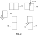
- a (112) is the size of a single exposure; B (118) is the result of precise alignment on x direction; C (117) is the result with error offset on x direction; B' (113) is the result of precise alignment on y direction; C' (115) is the result with error offset on y direction.
- stage assembly tolerance is usually off the allowed range; and the offset is not linear to the stage travel distance. Therefore, in the invention, offsets are measured at 10 or more evenly distributed points on both X and Y directions on a full-range printed square sample. At least second order polynomial error curves on both X and Y directions are fitted to the measure data by the least square method.
- Cs and Ds are polynomial coefficients calculated by the least square fitting method. These two error curves will be fed into the translation of the XY stages to compensate the offset thus ensure the accuracy of the stitching-printed sample is within the specifications.
- the theoretical target is ( X 0 ,Y 0 )
- the actual executed translation commands are ( X 0 +XError ( X 0 ,Y 0 ) ,Y 0 +YError ( X 0 ,Y 0 ) .
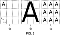
- the multi-scale P ⁇ SL provides basically three printing modes ( Figure 3 ).
- the XY stages When printing a single sample, which is smaller than the single exposure size of the finest lens, 2 ⁇ m in this invention, the XY stages will not move during printing. It is called single exposure mode. If multiple identical samples are needed, the XY states will move stepwise and print the same sample in an array. And this is called array exposure mode which is much faster for small volume production than repeating the single exposure mode.
- array exposure mode which is much faster for small volume production than repeating the single exposure mode.
- the system will further divide one layer into multiple sections and stitch the adjacent sections into a whole layer by overlapping 5 ⁇ m to 30 ⁇ m on the shared edges. This is the stitching exposure mode.
- the methods herein can be used as part of multi-scale P ⁇ SL printing process to establish a resin free surface, membrane or hard window as parallel to the surface of a sample stage.
- a resin free surface, membrane or hard window as parallel to the surface of a sample stage.
- three non-linear points, here forming the right-angle triangle shown are selected on the sample stage surface and sequentially aligned with the displacement sensor emission vector by moving the XY stages.
- the minimum distances between the points should be 1 cm to guarantee good accuracy.
- the sample stage should be adjusted to make sure the distance readings between the displacement sensor and each point are the same.
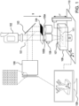
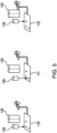
- FIG. 1 it shows a schematic drawing of a multi-scale projection micro stereolithography system; including a digital light processing panel (DLP) and light source 100; beam splitter 101; charge coupled device (CCD) 102; mirror 103; shutter 104; dual lenses 105A (2 ⁇ m) and 105B (10 ⁇ m); laser displacement sensor 106; membrane 107; resin vat 108; video unit 109; xyz stage assembly 110; and sample substrate 111; where z1 and z2 are the z directions and g is the direction of gravity.
- DLP digital light processing panel
- CCD charge coupled device
- FIG. 2 it shows stitching error in the x and y directions during stitch printing in a multi scale projection micro stereo lithography system, including 112 as the size of a single exposure; 113 is the result of precise alignment on y direction; 115 is the result with error offset in y direction 114, 118 is the result of precise alignment on x direction; and 117 is the result with error offset in x direction 116.
- Figure 3 it shows three exposure modes in a multi-scale projection micro stereolithography system, including printing borders 119, single exposure 120, stitching exposure 121, and array exposure 122.
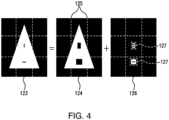
- FIG 4 it shows a printing sequence in a multi-scale stereolithography system, including layer image 123, 10 ⁇ m lens projection 124 with stich lines 125; and 2 ⁇ m lens projection 126 with stitch lines 127.
- Figure 5 it shows the procedures of leveling a sample stage using a laser displacement sensor in the multi-scale P ⁇ SL system, including laser displacement sensor 128; dual lens 129; step 1 130; step 2 131; and step 3, 132.
Landscapes
- Engineering & Computer Science (AREA)
- Chemical & Material Sciences (AREA)
- Materials Engineering (AREA)
- Manufacturing & Machinery (AREA)
- Physics & Mathematics (AREA)
- Mechanical Engineering (AREA)
- Optics & Photonics (AREA)
- Health & Medical Sciences (AREA)
- Toxicology (AREA)
- Microelectronics & Electronic Packaging (AREA)
- Exposure And Positioning Against Photoresist Photosensitive Materials (AREA)
Claims (11)
- Verfahren zum schnellen, hochauflösenden 3D-Drucken, wobei das Verfahren umfasst:Erzeugen eines digitalen 3D-Modells eines zu druckenden Testkörpers auf einem Computer, Zerschneiden des digitalen Modells in eine Sequenz von Bildern, wobei jedes Bild der Sequenz eine Schicht des digitalen 3D-Modells darstellt, und Übertragen eines Bildes aus der Sequenz von Bildern auf einen Mikroanzeigechip einer optischen Lichtmaschine (100), die den Mikroanzeigechip und eine Lichtquelle umfasst, wobei der Mikroanzeigechip eine Flüssigkristallanzeige oder eine digitale Lichtverarbeitungsplatte umfasst,Projizieren des Bildes zusammen mit Licht von der optischen Lichtmaschine (100) durch eine Projektionslinse (105A) eines Projektionslinsenkomplexes (105A, 105B) auf Druckmaterial (108),Bewirken, dass das Druckmaterial (108) in den hellen Bereichen des projizierten Bildes polymerisiert wird, während die dunklen Bereiche flüssig bleiben, undder Projektionslinsenkomplex (105A, 105B) zwei oder mehr Projektionslinsen mit unterschiedlichen Abbildungsverhältnissen umfasst, und wobei das Bild und das Licht jeweils nur durch eine Projektionslinse projiziert werden, undwobei der Projektionslinsenkomplex eine Doppelprojektionslinse ist, die zwei Projektionslinsen mit unterschiedlichen Abbildungsverhältnissen umfasst,wobei eine Linse eine höhere Auflösung und eine zweite Linse eine niedrigere Auflösung aufweist, wobei beide Linsen konstruktionsbedingt dieselbe Fokusebene teilen,wobei das Verfahren dadurch gekennzeichnet ist, dass optische Blenden (104) vor den Projektionslinsen (105A, 105B) verwendet werden, um die Bildprojektion von einer Projektionslinse auf eine andere Projektionslinse umzuschalten.
- Verfahren nach Anspruch 1, wobei die Doppelprojektionslinse eine höher auflösende 2 µm-Projektionslinse (105A) und eine niedriger auflösende 10 µm-Projektionslinse (105B) umfasst.
- Verfahren nach Anspruch 1 oder 2, wobei die Schichten durch Schichtbeschichtung mit einer Membran (107), freie Oberflächenbeschichtung, Sprühbeschichtung oder Beschichtung mit harten Fenstern hergestellt werden.
- Verfahren nach einem der Ansprüche 1 bis 3, wobei jedes Bild eine 5 bis 20 Mikrometer dicke Schicht des Modells darstellt.
- Verfahren nach Anspruch 3, wobei eine optisch klare Membran (107) zwischen dem Druckmaterial (108) und dem Projektionslinsenkomplex (105A, 105B) angeordnet ist, wobei die Membran (107) eine untere Oberfläche auf einer von dem Projektionslinsenkomplex (105A, 105B) abgewandten Seite aufweist, wobei die untere Oberfläche das Druckmaterial (108) während der Belichtung berührt, und wobei das Bild und das Licht von der Lichtquelle der optischen Lichtmaschine (100) durch eine Projektionslinse des Projektionslinsenkomplexes (105A, 105B) auf die untere Oberfläche der Membran (107) projiziert wird, um die Druckmaterialschicht (108) auszuhärten, und wenn eine Schicht fertig ist, ein Substrat (111) zum Halten des Testkörpers von der Membran wegbewegt wird, wodurch die Membran (107) von dem Testkörper getrennt wird, wonach der Testkörper zurück zur Membran (107) bewegt und in einem Abstand von der Membran angeordnet wird, der gleich der Dicke der nächsten zu druckenden Schicht ist, wobei während dieser Anordnung die Membran abgeflacht wird, um die nächste Schicht des Druckmaterials (108) zu definieren.
- Verfahren nach einem der Ansprüche 1 bis 5, ferner umfassend das Analysieren des Bildes der zu bedruckenden Schicht, um kleine Merkmale zu erkennen, die durch Fenster einer Belichtung mit höherer Auflösung isoliert sind, das Abtasten und Drucken der Schicht unter Verwendung der Projektionslinse (105B), die Belichtungen mit niedrigerer Auflösung liefert, gefolgt von einem Wechsel der optischen Blende (104), einer Umkehrung der Abtastung und einem Drucken der isolierten kleinen Merkmale unter Verwendung der Projektionslinse (105A), die die Belichtungen mit höherer Auflösung liefert.
- Verfahren nach einem der Ansprüche 1 bis 6 zum Drucken einer Schicht eines digitalen 3D-Modells oder eines Einzelschichtmodells, wobei die Schicht eine Größe aufweist, die die Größe einer einzelnen Bildbelichtung übersteigt, wobei das Verfahren ferner das Unterteilen der Schicht in mehrere Abschnitte und das Drucken der Abschnitte in der Weise umfasst, dass sich gemeinsame Kanten benachbarter Abschnitte um 5 µm bis 30 µm überlappen und die Abschnitte zu einer einzigen Gesamtschicht gestitcht werden.
- Verfahren nach einem der Ansprüche 1 bis 7, wobei die Bewegung des Substrats (111) zum Tragen des Drucktestkörpers und/oder des Druckprojektionssystems in X-, Y- und Z-Richtung durch drei Präzisionstische gesteuert wird.
- Verfahren nach Anspruch 8 zum Stitching und Array-Drucken, wobei das Substrat (111), das den Testkörper hält, in der XY-Ebene verschoben wird, während die Optik, die den Mikroanzeigechip und die Projektionslinse umfasst, fixiert wird; Verschieben der Optik, während das Substrat (111), das den Testkörper hält, fixiert wird, oder Verschieben sowohl des Substrats (111), das den Testkörper hält, als auch der Optik.
- Verfahren nach einem der Ansprüche 1 bis 9, wobei Fehlerkurven der kleinsten quadratischen Anpassung, die auf gemessenen Daten von tatsächlichen Drucktestkörpern basieren, in die Verschiebung der XY-Tische eingespeist werden, um mechanische Toleranzen zu kompensieren und so sicherzustellen, dass die Genauigkeit des stitch-gedruckten Testkörpers innerhalb der Spezifikationen liegt.
- Verfahren nach einem der Ansprüche 1 bis 10, wobei das Druckmaterial (108) ein lichthärtendes Harz ist.
Applications Claiming Priority (2)
| Application Number | Priority Date | Filing Date | Title |
|---|---|---|---|
| US202063104867P | 2020-10-23 | 2020-10-23 | |
| PCT/IB2021/059731 WO2022084921A1 (en) | 2020-10-23 | 2021-10-21 | A multi-scale system for projection micro stereolithography |
Publications (3)
| Publication Number | Publication Date |
|---|---|
| EP4232262A1 EP4232262A1 (de) | 2023-08-30 |
| EP4232262C0 EP4232262C0 (de) | 2025-01-08 |
| EP4232262B1 true EP4232262B1 (de) | 2025-01-08 |
Family
ID=78414688
Family Applications (1)
| Application Number | Title | Priority Date | Filing Date |
|---|---|---|---|
| EP21799341.9A Active EP4232262B1 (de) | 2020-10-23 | 2021-10-21 | Mehrskaliges system für mikroprojektionsstereolithographie |
Country Status (3)
| Country | Link |
|---|---|
| US (1) | US12420486B2 (de) |
| EP (1) | EP4232262B1 (de) |
| WO (1) | WO2022084921A1 (de) |
Families Citing this family (5)
| Publication number | Priority date | Publication date | Assignee | Title |
|---|---|---|---|---|
| EP3894184B1 (de) | 2018-12-10 | 2024-01-17 | BMF Precision Technology (Wuxi) Inc. | Verfahren zur steuerung der abmessungen in der projektions-mikrostereolithografie |
| WO2022084921A1 (en) | 2020-10-23 | 2022-04-28 | Bmf Material Technology Inc. | A multi-scale system for projection micro stereolithography |
| WO2023017488A1 (en) | 2021-08-13 | 2023-02-16 | Bmf Nano Material Technology Co., Ltd | System and method of low-waste multi-material resin printing |
| WO2024254138A1 (en) * | 2023-06-05 | 2024-12-12 | Pranav Soman | Multipath projection stereolithography system and method |
| WO2025077104A1 (zh) * | 2023-10-10 | 2025-04-17 | 深圳摩方新材科技有限公司 | 光固化3d打印装置的打印方法、装置及存储介质 |
Family Cites Families (75)
| Publication number | Priority date | Publication date | Assignee | Title |
|---|---|---|---|---|
| US4575330A (en) | 1984-08-08 | 1986-03-11 | Uvp, Inc. | Apparatus for production of three-dimensional objects by stereolithography |
| US5192559A (en) | 1990-09-27 | 1993-03-09 | 3D Systems, Inc. | Apparatus for building three-dimensional objects with sheets |
| JP3579798B2 (ja) | 1994-06-10 | 2004-10-20 | 独立行政法人 科学技術振興機構 | 光造形ファブリケーション法及びこれを利用した金属構造体の製造方法 |
| US6011577A (en) | 1997-06-30 | 2000-01-04 | Polaroid Corporation | Modular optical print head assembly |
| US5933278A (en) | 1997-06-30 | 1999-08-03 | Polaroid Corporation | Monolithic multi-faceted mirror for combining multiple beams from different light sources by reflection |
| US6607689B1 (en) | 2000-08-29 | 2003-08-19 | Micron Technology, Inc. | Layer thickness control for stereolithography utilizing variable liquid elevation and laser focal length |
| US20050219400A1 (en) | 2002-09-24 | 2005-10-06 | Hasselblad A/S | Image quality indicator |
| JP2004314406A (ja) * | 2003-04-15 | 2004-11-11 | Seiko Instruments Inc | 層厚可変のマイクロ光造形方法と層厚可変型マイクロ光造形装置 |
| JP4376649B2 (ja) | 2004-02-06 | 2009-12-02 | 宏 増原 | 異波長レーザー光を用いた多光束微小構造物光造形方法及び装置 |
| DE102004022606A1 (de) | 2004-05-07 | 2005-12-15 | Envisiontec Gmbh | Verfahren zur Herstellung eines dreidimensionalen Objekts mit verbesserter Trennung ausgehärteter Materialschichten von einer Bauebene |
| EP1732746B1 (de) | 2004-05-07 | 2011-04-27 | Envisiontec GmbH | Verfahren zur herstellung eines dreidimensionalen objekts mit verbesserter trennung ausgehärteter materialschichten von einer bauebene |
| US7892474B2 (en) | 2006-11-15 | 2011-02-22 | Envisiontec Gmbh | Continuous generative process for producing a three-dimensional object |
| KR100881273B1 (ko) | 2006-12-08 | 2009-02-05 | 한국전자통신연구원 | 무선 센서 네트워크의 센서 노드와 그 운용 방법 |
| JP5073284B2 (ja) | 2006-12-22 | 2012-11-14 | ローランドディー.ジー.株式会社 | 三次元造形装置 |
| US8487822B1 (en) | 2007-09-13 | 2013-07-16 | Rockwell Collins, Inc. | Adaptible antenna using liquid metal structures |
| US20110033887A1 (en) | 2007-09-24 | 2011-02-10 | Fang Nicholas X | Three-Dimensional Microfabricated Bioreactors with Embedded Capillary Network |
| JP2009083240A (ja) * | 2007-09-28 | 2009-04-23 | Sony Corp | 光造形装置 |
| DK2052693T4 (da) | 2007-10-26 | 2021-03-15 | Envisiontec Gmbh | Proces og fri-formfabrikationssystem til at fremstille en tredimensionel genstand |
| US20090186306A1 (en) | 2007-11-09 | 2009-07-23 | Klas Tommy Haraldsson | Polymeric microfluidic devices from liquid thermoset precursors |
| JP5088114B2 (ja) | 2007-12-04 | 2012-12-05 | ソニー株式会社 | 光造形装置 |
| US8828311B2 (en) | 2009-05-15 | 2014-09-09 | Board Of Regents, The University Of Texas System | Reticulated mesh arrays and dissimilar array monoliths by additive layered manufacturing using electron and laser beam melting |
| JP2011098484A (ja) | 2009-11-05 | 2011-05-19 | Sony Corp | 3次元光造形装置、3次元光造形方法及び造形物 |
| JP2011241450A (ja) | 2010-05-19 | 2011-12-01 | Keijiro Yamamoto | 積層造形方法及び積層造形装置 |
| WO2012021940A1 (en) | 2010-08-20 | 2012-02-23 | Zydex Pty Ltd | Apparatus and method for making an object |
| WO2012051598A2 (en) | 2010-10-14 | 2012-04-19 | Eye Ojo Corp. | Method and apparatus for curved circularly polarized lens |
| TWI506849B (zh) | 2011-07-20 | 2015-11-01 | Hon Hai Prec Ind Co Ltd | 天線 |
| US9120270B2 (en) | 2012-04-27 | 2015-09-01 | University Of Southern California | Digital mask-image-projection-based additive manufacturing that applies shearing force to detach each added layer |
| KR101958864B1 (ko) | 2012-09-17 | 2019-03-15 | 삼성전자 주식회사 | 액체 금속을 이용한 안테나 장치 및 그를 이용하는 휴대 단말기 |
| CN102928910A (zh) | 2012-11-22 | 2013-02-13 | 上海康耐特光学股份有限公司 | 一种偏光3d镜片及其制造方法 |
| MX352425B (es) | 2013-02-12 | 2017-11-23 | Carbon3D Inc | Método y aparato para fabricación tridimensional con alimentación a través de portador. |
| US9496675B1 (en) | 2013-07-09 | 2016-11-15 | Science Research Laboratory, Inc. | Method and reflective apparatus for combining high-power laser beams |
| US9360757B2 (en) | 2013-08-14 | 2016-06-07 | Carbon3D, Inc. | Continuous liquid interphase printing |
| US10144205B2 (en) | 2014-02-20 | 2018-12-04 | Global Filtration Systems | Apparatus and method for forming three-dimensional objects using a tilting solidification substrate |
| DE102014102720B4 (de) | 2014-02-28 | 2017-03-23 | Ushio Denki Kabushiki Kaisha | Anordnung zum Kühlen einer plasmabasierten Strahlungsquelle mit einer metallischen Kühlflüssigkeit und Verfahren zur Inbetriebnahme einer solchen Kühlanordnung |
| JP6454497B2 (ja) | 2014-08-26 | 2019-01-16 | 株式会社ミマキエンジニアリング | 立体物造形装置および立体物造形方法 |
| FR3027554B1 (fr) * | 2014-10-27 | 2020-02-07 | Centre National De La Recherche Scientifique | Procede d'impression en trois dimensions |
| WO2016109550A1 (en) | 2014-12-31 | 2016-07-07 | Carbon3D, Inc. | Three-dimensional printing of objects with breathing orifices |
| WO2016115095A1 (en) | 2015-01-13 | 2016-07-21 | Solid Innovations, Llc | Verification and adjustment systems and methods for additive manufacturing |
| CN107530972A (zh) | 2015-03-18 | 2018-01-02 | 埃托雷·毛里齐奥·科斯塔贝伯 | 具有改进的光学单元的立体光固化成型机 |
| CN104827667B (zh) | 2015-04-30 | 2017-05-24 | 北京敏速自动控制设备有限公司 | 打印平板调平方法及装置 |
| CN104991353B (zh) | 2015-07-28 | 2017-06-16 | 江苏视客新材料股份有限公司 | 复合曲率眼镜镜片的制造方法 |
| TWI568571B (zh) | 2015-08-28 | 2017-02-01 | 東友科技股份有限公司 | 列印平台調校系統及其調校方法 |
| CN105390056A (zh) | 2015-10-16 | 2016-03-09 | 南方医科大学 | 用于变形配准算法精度验证的高仿真腹部变形模体及其制备方法 |
| WO2017157851A1 (en) | 2016-03-14 | 2017-09-21 | Addifab Aps | Additive manufacturing device and system for manufacturing a sacrificial mould for creating an object |
| KR102233625B1 (ko) | 2016-08-23 | 2021-03-31 | 캐논 가부시끼가이샤 | 3차원 조형 장치 및 3차원 조형물의 제조 방법 |
| US20190111622A1 (en) | 2016-09-01 | 2019-04-18 | Oleg Yurevich KHALIP | Device and method for forming a three-dimensional object from a liquid polymer |
| US11214005B2 (en) | 2017-01-12 | 2022-01-04 | University Of Southern California | Surface projection tool for multi-axis additive manufacturing |
| US11167454B2 (en) | 2017-01-13 | 2021-11-09 | General Electric Company | Method and apparatus for continuously refreshing a recoater blade for additive manufacturing |
| US11085018B2 (en) | 2017-03-10 | 2021-08-10 | Prellis Biologics, Inc. | Three-dimensional printed organs, devices, and matrices |
| CN206718470U (zh) | 2017-04-20 | 2017-12-08 | 郭�东 | 一种液体界面的成型装置 |
| KR102017219B1 (ko) | 2017-05-16 | 2019-09-02 | 주식회사 힉스 | Sla 3d 프린터 |
| US10836104B2 (en) | 2017-07-10 | 2020-11-17 | NEXA3D Inc. | Three-dimensional printing system with rotating membrane |
| CN109291433A (zh) | 2017-07-24 | 2019-02-01 | 三纬国际立体列印科技股份有限公司 | 立体打印设备以及立体打印方法 |
| CN107756814A (zh) | 2017-11-28 | 2018-03-06 | 上海联泰科技股份有限公司 | 检测系统、方法及所适用的3d打印设备 |
| CN108437448B (zh) | 2018-02-02 | 2019-12-17 | 深圳摩方新材科技有限公司 | 一种微纳尺寸3d打印设备的光路精密装调方法 |
| US11285670B2 (en) | 2018-08-27 | 2022-03-29 | The Boeing Company | Laser fabrication additive system and method |
| US10994483B2 (en) | 2018-10-01 | 2021-05-04 | Eos Of North America, Inc. | Dual roller assembly for spreading material in additive manufacturing apparatus |
| US11951563B2 (en) | 2018-10-05 | 2024-04-09 | Vulcanforms Inc. | Additive manufacturing system with fixed build plate |
| CN109483872A (zh) | 2018-10-15 | 2019-03-19 | 无锡摩方精密科技有限公司 | 牺牲材料在微结构3d光固化打印中的应用 |
| CN109466061B (zh) | 2018-11-14 | 2020-07-31 | 厦门大学 | 一种基于电液动力耦合喷印的多材料3d打印设备 |
| EP3894184B1 (de) | 2018-12-10 | 2024-01-17 | BMF Precision Technology (Wuxi) Inc. | Verfahren zur steuerung der abmessungen in der projektions-mikrostereolithografie |
| CN109822891B (zh) | 2019-03-13 | 2023-09-08 | 重庆摩方科技有限公司 | 一种高精度大幅面立体投影3d打印系统及其打印方法 |
| CN110539482B (zh) | 2019-09-23 | 2021-04-30 | 深圳摩方新材科技有限公司 | 一种高速树脂涂层3d打印系统 |
| US11654617B2 (en) | 2020-02-05 | 2023-05-23 | Bmf Material Technology Inc. | Immersion projection micro stereolithography |
| US11351723B2 (en) | 2020-02-21 | 2022-06-07 | CALT Dynamics Limited | Systems, devices, and methods for manufacturing three dimensional objects via oxygen permeation of a gas permeable membrane |
| US11654619B2 (en) * | 2020-03-03 | 2023-05-23 | Bmf Material Technology Inc. | Immersion multi-material projection micro stereolithography with non-stick gas permeable transparent membrane |
| WO2021103502A1 (zh) | 2020-06-19 | 2021-06-03 | 深圳摩方新材科技有限公司 | 多通道3d打印方法及3d打印系统 |
| CN111873431B (zh) | 2020-06-19 | 2022-03-29 | 深圳摩方新材科技有限公司 | 多通道3d打印方法及3d打印系统 |
| CN111873433B (zh) | 2020-06-19 | 2022-04-12 | 深圳摩方新材科技有限公司 | 树脂涂层3d打印方法及系统 |
| WO2022084921A1 (en) | 2020-10-23 | 2022-04-28 | Bmf Material Technology Inc. | A multi-scale system for projection micro stereolithography |
| CN112549537B (zh) * | 2020-11-13 | 2022-07-12 | 深圳摩方新材科技有限公司 | 一种双镜头组合精度提速3d打印装置及打印方法 |
| US12397505B2 (en) | 2021-03-25 | 2025-08-26 | Solventum Intellectual Properties Company | Additive manufacturing apparatus including two light engines and a light altering structure and a method of additive manufacturing a three-dimensional object |
| EP4326529A1 (de) | 2021-04-19 | 2024-02-28 | BMF Material Technology Inc. | Systeme und verfahren zur freisetzung einer membran beim 3d-harzdruck |
| WO2023017488A1 (en) | 2021-08-13 | 2023-02-16 | Bmf Nano Material Technology Co., Ltd | System and method of low-waste multi-material resin printing |
| CN113927897B (zh) | 2021-09-18 | 2024-03-15 | 深圳摩方新材科技有限公司 | 一种高利用率的多材料树脂3d打印系统和方法 |
-
2021
- 2021-10-21 WO PCT/IB2021/059731 patent/WO2022084921A1/en not_active Ceased
- 2021-10-21 US US18/033,405 patent/US12420486B2/en active Active
- 2021-10-21 EP EP21799341.9A patent/EP4232262B1/de active Active
Also Published As
| Publication number | Publication date |
|---|---|
| EP4232262C0 (de) | 2025-01-08 |
| WO2022084921A1 (en) | 2022-04-28 |
| US12420486B2 (en) | 2025-09-23 |
| US20230398739A1 (en) | 2023-12-14 |
| EP4232262A1 (de) | 2023-08-30 |
Similar Documents
| Publication | Publication Date | Title |
|---|---|---|
| EP4232262B1 (de) | Mehrskaliges system für mikroprojektionsstereolithographie | |
| US11654617B2 (en) | Immersion projection micro stereolithography | |
| KR100743289B1 (ko) | 몰드, 패턴형성방법 및 패턴형성장치 | |
| EP2186625B1 (de) | Verfahren zur Herstellung eines dreidimensionalen Gegenstandes | |
| US20210299952A1 (en) | Roller-membrane layering micro stereolithography | |
| EP3285992B1 (de) | Vorrichtung und verfahren zur herstellung dreidimensionaler objekte mittels abtastungsachsenkompensierung und dynamischem offset | |
| WO2021114602A1 (zh) | 3d打印方法及3d打印系统 | |
| CN113059796B (zh) | 3d打印设备的标定机构、方法、系统及存储介质 | |
| CN108312505A (zh) | 一种dmd扫描成像的3d成型装置及方法 | |
| CN111873432B (zh) | 3d打印方法及3d打印系统 | |
| CN102566325B (zh) | 光学加工系统和方法 | |
| JP2008251797A (ja) | 基準位置計測装置及び方法、並びに描画装置 | |
| EP3894184B1 (de) | Verfahren zur steuerung der abmessungen in der projektions-mikrostereolithografie | |
| EP3969963B1 (de) | System und verfahren zum belichten eines materials mit bildern | |
| CN115453839B (zh) | 一种面向dlp 3d打印的单光源水平校准方法 | |
| CN117241000A (zh) | 一种面向dlp面曝光3d打印的多光源像素级拼接方法 | |
| JPH07105323B2 (ja) | 露光方法 | |
| US20120314050A1 (en) | Imaging apparatus and control method therefor | |
| US20070024938A1 (en) | Method and apparatus using hologram masks for printing composite patterns onto large substrates | |
| CN105904727A (zh) | 基于dlp的光固化3d打印成型方法、系统及设备 | |
| US7522323B2 (en) | Method and apparatus for printing a pattern with improved focus correction and higher throughput | |
| CN207972294U (zh) | 一种dmd扫描成像的3d成型装置 | |
| JP2003039562A (ja) | 光造形システムにおけるレーザビームの偏向制御方法 | |
| Cao et al. | Galvanometer Based In-situ Imaging and Inspection System with Variable Ranges and Resolutions | |
| CN118528546B (zh) | 一种sla与dlp增材制造光学对准与液面监测方法 |
Legal Events
| Date | Code | Title | Description |
|---|---|---|---|
| STAA | Information on the status of an ep patent application or granted ep patent |
Free format text: STATUS: UNKNOWN |
|
| STAA | Information on the status of an ep patent application or granted ep patent |
Free format text: STATUS: THE INTERNATIONAL PUBLICATION HAS BEEN MADE |
|
| PUAI | Public reference made under article 153(3) epc to a published international application that has entered the european phase |
Free format text: ORIGINAL CODE: 0009012 |
|
| STAA | Information on the status of an ep patent application or granted ep patent |
Free format text: STATUS: REQUEST FOR EXAMINATION WAS MADE |
|
| 17P | Request for examination filed |
Effective date: 20230323 |
|
| AK | Designated contracting states |
Kind code of ref document: A1 Designated state(s): AL AT BE BG CH CY CZ DE DK EE ES FI FR GB GR HR HU IE IS IT LI LT LU LV MC MK MT NL NO PL PT RO RS SE SI SK SM TR |
|
| DAV | Request for validation of the european patent (deleted) | ||
| DAX | Request for extension of the european patent (deleted) | ||
| GRAP | Despatch of communication of intention to grant a patent |
Free format text: ORIGINAL CODE: EPIDOSNIGR1 |
|
| STAA | Information on the status of an ep patent application or granted ep patent |
Free format text: STATUS: GRANT OF PATENT IS INTENDED |
|
| INTG | Intention to grant announced |
Effective date: 20240805 |
|
| GRAS | Grant fee paid |
Free format text: ORIGINAL CODE: EPIDOSNIGR3 |
|
| GRAA | (expected) grant |
Free format text: ORIGINAL CODE: 0009210 |
|
| STAA | Information on the status of an ep patent application or granted ep patent |
Free format text: STATUS: THE PATENT HAS BEEN GRANTED |
|
| AK | Designated contracting states |
Kind code of ref document: B1 Designated state(s): AL AT BE BG CH CY CZ DE DK EE ES FI FR GB GR HR HU IE IS IT LI LT LU LV MC MK MT NL NO PL PT RO RS SE SI SK SM TR |
|
| REG | Reference to a national code |
Ref country code: GB Ref legal event code: FG4D |
|
| REG | Reference to a national code |
Ref country code: CH Ref legal event code: EP |
|
| REG | Reference to a national code |
Ref country code: DE Ref legal event code: R096 Ref document number: 602021024741 Country of ref document: DE |
|
| REG | Reference to a national code |
Ref country code: IE Ref legal event code: FG4D |
|
| U01 | Request for unitary effect filed |
Effective date: 20250121 |
|
| U07 | Unitary effect registered |
Designated state(s): AT BE BG DE DK EE FI FR IT LT LU LV MT NL PT RO SE SI Effective date: 20250127 |
|
| PG25 | Lapsed in a contracting state [announced via postgrant information from national office to epo] |
Ref country code: RS Free format text: LAPSE BECAUSE OF FAILURE TO SUBMIT A TRANSLATION OF THE DESCRIPTION OR TO PAY THE FEE WITHIN THE PRESCRIBED TIME-LIMIT Effective date: 20250408 |
|
| PG25 | Lapsed in a contracting state [announced via postgrant information from national office to epo] |
Ref country code: PL Free format text: LAPSE BECAUSE OF FAILURE TO SUBMIT A TRANSLATION OF THE DESCRIPTION OR TO PAY THE FEE WITHIN THE PRESCRIBED TIME-LIMIT Effective date: 20250108 |
|
| PG25 | Lapsed in a contracting state [announced via postgrant information from national office to epo] |
Ref country code: ES Free format text: LAPSE BECAUSE OF FAILURE TO SUBMIT A TRANSLATION OF THE DESCRIPTION OR TO PAY THE FEE WITHIN THE PRESCRIBED TIME-LIMIT Effective date: 20250108 |
|
| PG25 | Lapsed in a contracting state [announced via postgrant information from national office to epo] |
Ref country code: NO Free format text: LAPSE BECAUSE OF FAILURE TO SUBMIT A TRANSLATION OF THE DESCRIPTION OR TO PAY THE FEE WITHIN THE PRESCRIBED TIME-LIMIT Effective date: 20250408 Ref country code: IS Free format text: LAPSE BECAUSE OF FAILURE TO SUBMIT A TRANSLATION OF THE DESCRIPTION OR TO PAY THE FEE WITHIN THE PRESCRIBED TIME-LIMIT Effective date: 20250508 |
|
| PG25 | Lapsed in a contracting state [announced via postgrant information from national office to epo] |
Ref country code: HR Free format text: LAPSE BECAUSE OF FAILURE TO SUBMIT A TRANSLATION OF THE DESCRIPTION OR TO PAY THE FEE WITHIN THE PRESCRIBED TIME-LIMIT Effective date: 20250108 |
|
| PG25 | Lapsed in a contracting state [announced via postgrant information from national office to epo] |
Ref country code: GR Free format text: LAPSE BECAUSE OF FAILURE TO SUBMIT A TRANSLATION OF THE DESCRIPTION OR TO PAY THE FEE WITHIN THE PRESCRIBED TIME-LIMIT Effective date: 20250409 |
|
| PG25 | Lapsed in a contracting state [announced via postgrant information from national office to epo] |
Ref country code: SM Free format text: LAPSE BECAUSE OF FAILURE TO SUBMIT A TRANSLATION OF THE DESCRIPTION OR TO PAY THE FEE WITHIN THE PRESCRIBED TIME-LIMIT Effective date: 20250108 |
|
| PG25 | Lapsed in a contracting state [announced via postgrant information from national office to epo] |
Ref country code: CZ Free format text: LAPSE BECAUSE OF FAILURE TO SUBMIT A TRANSLATION OF THE DESCRIPTION OR TO PAY THE FEE WITHIN THE PRESCRIBED TIME-LIMIT Effective date: 20250108 |
|
| PG25 | Lapsed in a contracting state [announced via postgrant information from national office to epo] |
Ref country code: SK Free format text: LAPSE BECAUSE OF FAILURE TO SUBMIT A TRANSLATION OF THE DESCRIPTION OR TO PAY THE FEE WITHIN THE PRESCRIBED TIME-LIMIT Effective date: 20250108 |
|
| PLBE | No opposition filed within time limit |
Free format text: ORIGINAL CODE: 0009261 |
|
| STAA | Information on the status of an ep patent application or granted ep patent |
Free format text: STATUS: NO OPPOSITION FILED WITHIN TIME LIMIT |
|
| U20 | Renewal fee for the european patent with unitary effect paid |
Year of fee payment: 5 Effective date: 20251027 |