EP4231300B1 - Antischmelzverbindungsspeicherzelle und datenschreib-/leseschaltung damit sowie antischmelzverbindungsspeicher und betriebsverfahren dafür - Google Patents
Antischmelzverbindungsspeicherzelle und datenschreib-/leseschaltung damit sowie antischmelzverbindungsspeicher und betriebsverfahren dafür Download PDFInfo
- Publication number
- EP4231300B1 EP4231300B1 EP21952553.2A EP21952553A EP4231300B1 EP 4231300 B1 EP4231300 B1 EP 4231300B1 EP 21952553 A EP21952553 A EP 21952553A EP 4231300 B1 EP4231300 B1 EP 4231300B1
- Authority
- EP
- European Patent Office
- Prior art keywords
- fuse memory
- varactor
- pmos transistor
- drain
- source
- Prior art date
- Legal status (The legal status is an assumption and is not a legal conclusion. Google has not performed a legal analysis and makes no representation as to the accuracy of the status listed.)
- Active
Links
Images


Classifications
-
- H—ELECTRICITY
- H10—SEMICONDUCTOR DEVICES; ELECTRIC SOLID-STATE DEVICES NOT OTHERWISE PROVIDED FOR
- H10B—ELECTRONIC MEMORY DEVICES
- H10B20/00—Read-only memory [ROM] devices
- H10B20/20—Programmable ROM [PROM] devices comprising field-effect components
- H10B20/25—One-time programmable ROM [OTPROM] devices, e.g. using electrically-fusible links
-
- G—PHYSICS
- G11—INFORMATION STORAGE
- G11C—STATIC STORES
- G11C17/00—Read-only memories programmable only once; Semi-permanent stores, e.g. manually-replaceable information cards
- G11C17/14—Read-only memories programmable only once; Semi-permanent stores, e.g. manually-replaceable information cards in which contents are determined by selectively establishing, breaking or modifying connecting links by permanently altering the state of coupling elements, e.g. PROM
- G11C17/16—Read-only memories programmable only once; Semi-permanent stores, e.g. manually-replaceable information cards in which contents are determined by selectively establishing, breaking or modifying connecting links by permanently altering the state of coupling elements, e.g. PROM using electrically-fusible links
-
- G—PHYSICS
- G11—INFORMATION STORAGE
- G11C—STATIC STORES
- G11C17/00—Read-only memories programmable only once; Semi-permanent stores, e.g. manually-replaceable information cards
- G11C17/14—Read-only memories programmable only once; Semi-permanent stores, e.g. manually-replaceable information cards in which contents are determined by selectively establishing, breaking or modifying connecting links by permanently altering the state of coupling elements, e.g. PROM
- G11C17/18—Auxiliary circuits, e.g. for writing into memory
-
- G—PHYSICS
- G11—INFORMATION STORAGE
- G11C—STATIC STORES
- G11C7/00—Arrangements for writing information into, or reading information out from, a digital store
- G11C7/10—Input/output [I/O] data interface arrangements, e.g. I/O data control circuits, I/O data buffers
- G11C7/1051—Data output circuits, e.g. read-out amplifiers, data output buffers, data output registers, data output level conversion circuits
- G11C7/1069—I/O lines read out arrangements
-
- G—PHYSICS
- G11—INFORMATION STORAGE
- G11C—STATIC STORES
- G11C7/00—Arrangements for writing information into, or reading information out from, a digital store
- G11C7/10—Input/output [I/O] data interface arrangements, e.g. I/O data control circuits, I/O data buffers
- G11C7/1078—Data input circuits, e.g. write amplifiers, data input buffers, data input registers, data input level conversion circuits
- G11C7/1096—Write circuits, e.g. I/O line write drivers
-
- G—PHYSICS
- G11—INFORMATION STORAGE
- G11C—STATIC STORES
- G11C7/00—Arrangements for writing information into, or reading information out from, a digital store
- G11C7/22—Read-write [R-W] timing or clocking circuits; Read-write [R-W] control signal generators or management
-
- H—ELECTRICITY
- H10—SEMICONDUCTOR DEVICES; ELECTRIC SOLID-STATE DEVICES NOT OTHERWISE PROVIDED FOR
- H10D—INORGANIC ELECTRIC SEMICONDUCTOR DEVICES
- H10D89/00—Aspects of integrated devices not covered by groups H10D84/00 - H10D88/00
- H10D89/10—Integrated device layouts
Definitions
- the present invention belongs to the field of integrated circuit design, and particularly relates to an anti-fuse memory cell and a data read-write circuit thereof.
- OTP One-Time Programmable
- An early floating-gate OTP cannot be reliably used for a thin gate oxide layer of 65 nm or in a more advanced technology, so an anti-fuse solution is generally adopted in the advanced technology.
- a structure and an arrangement density of the memory cells directly determine an area of the memory, thus affecting the cost thereof.
- reliability and a reading speed that is, a running speed of the MCU, are also the main indicators of the memory.
- Document US2017/372790 A1 discloses an anti-fuse device including a gate insulating film formed on a semiconductor substrate, a gate electrode formed on the gate insulating film, and a salicide layer formed on a first portion of the gate electrode such that a second portion of the gate electrode omits the salicide layer, wherein a hard breakdown of at least a portion of the gate insulating film occurred at a time of programming the anti-fuse device.
- the present invention in order to solve the problems of large area, high on-resistance and low reading speed and reliability of an anti-fuse memory in the prior art, the present invention provides an anti-fuse memory unit and a data read-write circuit thereof.
- Another object of the present invention is to provide an anti-fuse memory.
- an anti-fuse memory cell comprises a base, wherein the base is provided with an N-well and a non-N-well region; the non-N-well region is provided with a first NMOS transistor; a gate of the first NMOS transistor is used for inputting a first selection signal; the N-well is provided with a PMOS transistor and a varactor; the gate of the PMOS transistor and a gate of the varactor are both connected to a drain of the first NMOS transistor; and the N-well, a drain, a source and a substrate of the PMOS transistor and a drain, a source, and a substrate of the varactor are all connected to a controllable power supply; the source of the PMOS transistor is adjacent to the source of the varactor; the drain of the PMOS transistor is adjacent to the drain of the varactor; an active region of the PMOS transistor is adjacent to an active region of the varactor; the gate of the PMOS transistor is adjacent to the gate of the varactor or the PMOS transistor and the varactor share one gate
- the first NMOS transistor is an IO device or a high-voltage process device
- at least one of the PMOS and the varactor is a CORE device or a low-voltage process device.
- controllable power supply comprises two states: a programmed high voltage and a normal operating voltage, wherein the normal operating voltage is a normal state of the controllable power supply and is used for reading data; and the programmed high voltage is only used in programming, and an OTP memory is usually programmed only once, so the programmed high voltage is usually used only once.
- a data read-write circuit comprises the anti-fuse memory cell above, further comprising a second NMOS transistor, a reference signal and a comparator, wherein a gate of the second NMOS transistor is used for inputting a second selection signal, a drain of the second NMOS transistor is connected to the source of the first NMOS transistor, a source of the second NMOS transistor and the reference signal are connected to an input end of the comparator, and an output end of the comparator outputs a logic level.
- An anti-fuse memory comprises a plurality of anti-fuse memory cells above, wherein the anti-fuse memory cells are connected in a matrix, and different anti-fuse memory cells are input with different first selection signals or different second selection signals.
- two adjacent anti-fuse memories connected to the same second selection signal at least share the source or the drain of one PMOS transistor and share the source or the drain of one varactor, so as to save chip area.
- An operation method for the anti-fuse memory above comprises a data writing method, wherein the data writing method comprises: switching the controllable power supply to the programmed high voltage, taking the anti-fuse memory cell needing to write a value as a writing target cell, addressing the writing target cell, and setting a first selection signal and a second selection signal of the writing target cell to a high level; and setting at least one of the first selection signal and the second selection signal to be 0 V for anti-fuse memory cells that do not need to write values.
- the operation method for the anti-fuse memory comprises a data reading method, wherein the data reading method comprises: switching the controllable power supply to the normal operating voltage, wherein the normal operating voltage does not exceed 30% of the programmed high voltage, taking the anti-fuse memory cell needing to be read as a reading target cell, addressing the reading target cell, setting a first selection signal and a second selection signal of the reading target cell to a high level and outputting a logic level of 1 or 0 by the comparator.
- the varactor in the present invention is equivalent to the special NMOS transistor placed in the N-well, which is completely separated and modeled in some processes, and is called a Varactor. It is found from a principle of a CMOS process, and the principle analysis of electronics and experiments that, this special device is also completely feasible in ordinary CMOS manufacturing processes without varactor models, and no extra mask or process flow is added.
- the first NMOS When a reading operation is carried out during operation, the first NMOS is turned on, but because the controllable power supply of the N-well is at a normal operating voltage, which is relatively low, a voltage difference between the gates that have been broken down and formed resistive connection and the N-well is small, so that the P inversion or an incomplete inversion is no longer formed.
- An original N-type layer under the gate herein has the same polarity with the source and the drain of the varactor, and if there is the P inversion under the gate, the P inversion layer will have the same polarity with the source and the drain of the PMOS, and in either case, the present invention can provide reliable low-resistance conduction by means of the source and the drain with two polarities, thus improving a chip yield, increasing a reading speed and greatly simplifying a design of a comparator.
- the N-well has a minimum width
- the width still does not exceed a width of the active region capable of being contained by the N-well under the minimum width rule, which means that an area of the N-well is not increased.
- the varactor which is namely the special NMOS, is adjacent to the PMOS, which not only increases a gate area of the programmable memory cell, but also is used as N-well tap of the PMOS transistor, thus saving the overall area and reducing the on-resistance after programming.
- the present invention provides the anti-fuse memory cell and the data read-write circuit thereof, which, compared with the prior art, have the following beneficial effects.
- the first NMOS transistor Q1 is an IO device or a high-voltage process device of 2.5 V to 5 V, such as 2.5 V/3.3 V/5 V, and may withstand a higher programming voltage during occasional programming for a short time
- the PMOS transistor and the varactor are a CORE device or a low-voltage process device of 0.7 Vto 1.8 V, such as 0.9 V/1.0 V/1.2 V/1.5 V/1.8 V
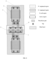
- the PMOS transistor 6 and the varactor 7 are in one N-well region together.
- a channel of the varactor 7 is formed by the N-well, and the source and the drain of the varactor are an N+ implanted layer in connection with the N-well, and are connected to the power supply, so that the drain and/or the source of the varactor 7 may be reused as a N-well tap of the PMOS transistor 6.
- the PMOS transistor 6 has no dedicated N-well tap. In this way, an area can be reduced, so that an arrangement density of the anti-fuse memory cell is higher.
- the controllable power supply VPD comprises a programmed high voltage and a normal operating voltage, wherein the high voltage is 4 V to 7 V, such as 5 V; and the normal operating voltage is a relatively low voltage of 0.7 V to 1.8 V, such as 1.2 V Other values may also be selected according to different environments.
- the VPD inputs the high voltage; and during data reading, the VPD inputs the low voltage.
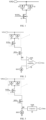
- FIG. 2 shows a data read-write circuit of the anti-fuse memory cell
- the data read-write circuit comprises the anti-fuse memory cell 1 above, a second NMOS transistor Q4,a reference current source IREF and a comparator, wherein a gate of the second NMOS transistor is used for inputting a second selection signal, a drain of the second NMOS transistor is connected to the source of the first NMOS transistor, a source of the second NMOS transistor is connected to a first input end of the comparator, a second input end of the comparator is connected to the reference current source IREF, and an output end of the comparator outputs a logic level.
- a voltage comparator may also be used, and a reference voltage source is used accordingly.
- the implementation mode may also be as shown in FIG. 3 , and the source of the second NMOS transistor is connected to the reference current source and the comparator.
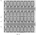
- the anti-fuse memory comprises a plurality of anti-fuse memory cells, wherein the anti-fuse memory cells are connected in a matrix, and as shown in FIG. 9 , different anti-fuse memory cells are input with different first selection signals WSN or different second selection signals BSN (the read-write circuit part is not drawn). The memory cell needing to write a value is selected through the first selection signal WSN and the second selection signal BSN.
- FIG. 10 is a layout diagram of an array of the matrix.
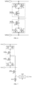
- FIG. 6 is a diagram of a circuit of a 2-bit anti-fuse memory cell
- FIG. 7 is a diagram of a read-write circuit of the 2-bit anti-fuse memory cell.
- Two cells have first selection signals WSNm and WSNn respectively, and share a second selection signal BSNm.
- two adjacent anti-fuse memories connected to the same second selection signal may share the source or the drain of one PMOS transistor, share the source or the drain of one varactor, and share one N-well region 3.
- An operation method for the anti-fuse memory comprises a data writing method and a data reading method, which are specifically as follows.
- the anti-fuse memory cell needing to write an effective value is taken as a writing target cell, and as shown in FIG. 7 , a first selection signal WSNm and a second selection signal BSNm corresponding to the writing target cell are both set to a high level, such as 3.3 V, according to position addressing of the writing target cell, so that the first NMOS transistor Q1 and the second NMOS transistor Q4 are turned on.
- a high level such as 3.3 V
- the gate of the PMOS transistor and the gate of the capacitor transistor are pulled to 0 V
- voltages at two ends of a gate capacitor of the PMOS transistor generally do not exceed 2 V, but at this moment a voltage difference between the two ends can reach 5 V
- the high voltage causes breakdown between the gate and source/drain/substrate inside the PMOS transistor or the varactor, so that the memory cell forms resistive connection and forms a conductive path between the gate and source/drain/substrate, which is equivalent to an on-resistance. Then the writing operation is completed.
- At least one of the first selection signal WSNm and the second selection signal BSNm of the memory cell is set to be 0 V, so that at least one of the first NMOS transistor Q1 and the second NMOS transistor Q4 of the memory cell is not turned on, and the memory cell is kept in an insulated state.
- the controllable power supply is switched to the relatively low normal operating voltage, wherein the low voltage does not exceed 30% of the programmed high voltage, such as 1.2 V, and the source, the drain and the substrate of the PMOS transistor and the source, the drain and the substrate of the varactor are pulled to a low-voltage power supply potential VDDK of 1.2 V
- the memory cell needing to be read is taken as a reading target cell, a first selection signal and a second selection signal of the reading target cell are both set to a high level, such as 3.3 V or 1.8 V, and the first NMOS transistor and the second NMOS transistor are turned on.
- the gate capacitor of at least one of the PMOS transistor and the varactor is not broken down, so that there is no resistive path, and the memory cell is in an insulated state.
- the IREF pulls down the input of the comparator to 0 V Therefore, the output of the comparator is logically low.
- Second Embodiment lies in that, in the read-write circuit of the anti-fuse memory cell, a BX point of the source of the second NMOS transistor is also connected with a pull-up transistor and a pull-down transistor.
- the BX point is pulled down to a low potential of 0 V except that the first selection signal WSNm and the second selection signal BSNm of the writing target cell are both set to a high level; and for the memory cell that does not need to write the effectively values or the logic 0 is written, the BX point is pulled up to a high potential, such as 4.3 V (VPD-0.7 V).
- VPD-0.7 V the low potential
Landscapes
- Read Only Memory (AREA)
- Semiconductor Memories (AREA)
- Dram (AREA)
Claims (8)
- Eine Antischmelzverbindungsspeicherzelle, die eine Basis beinhaltet, wobei die Basis mit einer N-Wanne und einer Nicht-N-Wannen-Region bereitgestellt ist; wobei die Nicht-N-Wannen-Region mit einem ersten NMOS-Transistor (Q1) bereitgestellt ist;ein Gatter des ersten NMOS-Transistors zum Einspeisen eines ersten Auswahlsignals (WSNm) verwendet wird; wobei die N-Wanne mit einem PMOS-Transistor (Q2) und einem Varaktor (Q3) bereitgestellt ist; ein Gatter des PMOS-Transistors und ein Gatter des Varaktors beide mt einer Senke des ersten NMOS-Transistors verbunden sind; und wobei die N-Wanne, eine Senke, eine Quelle und ein Substrat des PMOS-Transistors und eine Senke, eine Quelle und ein Substrat des Varaktors alle mit einer steuerbaren Stromversorgung (VPD) verbunden sind;die Quelle des PMOS-Transistors benachbart zu der Quelle des Varaktors ist; die Senke des PMOS-Transistors benachbart zu der Senke des Varaktors ist; eine aktive Region des PMOS-Transistors benachbart zu einer aktiven Region des Varaktors ist; das Gatter des PMOS-Transistors benachbart zu dem Gatter des Varaktors ist oder der PMOS-Transistor und der Varaktor ein Gatter teilen und mindestens eines von der Senke und der Quelle des Varaktors N-Typ-implantiert ist und als ein N-Wannen-Abgriff des PMOS-Transistors verwendet wird; und der PMOS-Transistor keinen dedizierten N-Wannen-Abgriff aufweist.
- Antischmelzverbindungsspeicherzelle gemäß Anspruch 1, wobei der erste NMOS-Transistor eine IO-Vorrichtung oder eine Hochspannungsvorgangsvorrichtung ist und mindestens eines von dem PMOS und dem Varaktor eine CORE-Vorrichtung oder eine Niedrigspannungsvorgangsvorrichtung ist.
- Antischmelzverbindungsspeicherzelle gemäß Anspruch 1 oder 2, wobei die steuerbare Stromversorgung eine programmierte Hochspannung und eine normale Betriebsspannung beinhaltet.
- Eine Daten-Schreib-Lese-Schaltung, die die Antischmelzverbindungsspeicherzelle gemäß Anspruch 1 oder 2 beinhaltet und ferner einen zweiten NMOS-Transistor, ein Referenzsignal und einen Komparator beinhaltet, wobei ein Gatter des zweiten NMOS-Transistors zum Einspeisen eines zweiten Auswahlsignals verwendet wird, eine Senke des zweiten NMOS-Transistors mit der Quelle des ersten NMOS-Transistors verbunden ist, eine Quelle des zweiten NMOS-Transistors und das Referenzsignal mit einem Einspeisungsende des Komparators verbunden sind und ein Ausgabeende des Komparators einen logischen Pegel ausgibt.
- Ein Antischmelzverbindungsspeicher, der eine Vielzahl von
Antischmelzverbindungsspeicherzellen gemäß einem der Ansprüche 1 bis 4 beinhaltet, wobei die Antischmelzverbindungsspeicherzellen in einer Matrix verbunden sind und unterschiedliche Antischmelzverbindungsspeicherzellen mit unterschiedlichen ersten Auswahlsignalen oder unterschiedlichen zweiten Auswahlsignalen gespeist werden. - Antischmelzverbindungsspeicher gemäß Anspruch 5, wobei zwei benachbarte Antischmelzverbindungsspeicher, die mit demselben zweiten Auswahlsignal verbunden sind, mindestens die Quelle oder die Senke eines PMOS-Transistors teilen und die Quelle oder die Senke eines Varaktors teilen.
- Ein Betriebsverfahren für den Antischmelzverbindungsspeicher gemäß Anspruch 5 oder 6, das ein Datenschreibverfahren beinhaltet, wobei das Datenschreibverfahren Folgendes beinhaltet:
Umschalten der steuerbaren Stromversorgung auf die programmierte Hochspannung, Festlegen der Antischmelzverbindungsspeicherzelle, die einen Wert schreiben soll, als eine Schreibzielzelle, Ansprechen der Schreibzielzelle und Einstellen sowohl eines ersten Auswahlsignals als auch eines zweiten Auswahlsignals der Schreibzielzelle auf einen H-Pegel; und andererseits Einstellen von mindestens einem von dem ersten Auswahlsignal und dem zweiten Auswahlsignal auf 0 V für Antischmelzverbindungsspeicherzellen, die keine Werte schreiben müssen. - Betriebsverfahren für den Antischmelzverbindungsspeicher gemäß Anspruch 7, das ein Datenleseverfahren beinhaltet, wobei das Datenleseverfahren Folgendes beinhaltet: Umschalten der steuerbaren Stromversorgung auf die normale Betriebsspannung, wobei die normale Betriebsspannung 30 % der programmierten Hochspannung nicht überschreitet, Festlegen der Antischmelzverbindungsspeicherzelle, die gelesen werden soll, als eine Ziellesezelle, Ansprechen der Ziellesezelle, Einstellen eines ersten Auswahlsignals und eines zweiten Auswahlsignals der Ziellesezelle auf einen H-Pegel und Ausgeben eines logischen Pegels von 1 oder 0 durch den Komparator.
Applications Claiming Priority (2)
| Application Number | Priority Date | Filing Date | Title |
|---|---|---|---|
| CN202110889462.3A CN113345506B (zh) | 2021-08-04 | 2021-08-04 | 一种反熔丝存储单元及其数据读写电路 |
| PCT/CN2021/124181 WO2023010687A1 (zh) | 2021-08-04 | 2021-10-15 | 一种反熔丝存储单元及其数据读写电路、反熔丝存储器及操作方法 |
Publications (3)
| Publication Number | Publication Date |
|---|---|
| EP4231300A1 EP4231300A1 (de) | 2023-08-23 |
| EP4231300A4 EP4231300A4 (de) | 2024-05-29 |
| EP4231300B1 true EP4231300B1 (de) | 2024-12-18 |
Family
ID=77480570
Family Applications (1)
| Application Number | Title | Priority Date | Filing Date |
|---|---|---|---|
| EP21952553.2A Active EP4231300B1 (de) | 2021-08-04 | 2021-10-15 | Antischmelzverbindungsspeicherzelle und datenschreib-/leseschaltung damit sowie antischmelzverbindungsspeicher und betriebsverfahren dafür |
Country Status (4)
| Country | Link |
|---|---|
| US (1) | US11948649B2 (de) |
| EP (1) | EP4231300B1 (de) |
| CN (1) | CN113345506B (de) |
| WO (1) | WO2023010687A1 (de) |
Families Citing this family (4)
| Publication number | Priority date | Publication date | Assignee | Title |
|---|---|---|---|---|
| CN113345506B (zh) * | 2021-08-04 | 2021-11-05 | 南京沁恒微电子股份有限公司 | 一种反熔丝存储单元及其数据读写电路 |
| CN114171096B (zh) * | 2021-12-03 | 2025-09-09 | 中国电子科技集团公司第五十八研究所 | 一种读取时间可控的反熔丝存储器读取电路 |
| US12119069B2 (en) | 2021-12-03 | 2024-10-15 | Wuxi Esiontech Co., Ltd. | Anti-fuse memory reading circuit with controllable reading time |
| CN116566373B (zh) * | 2023-07-10 | 2023-09-12 | 中国电子科技集团公司第五十八研究所 | 一种高可靠抗辐射反熔丝开关单元结构 |
Family Cites Families (8)
| Publication number | Priority date | Publication date | Assignee | Title |
|---|---|---|---|---|
| JP5590842B2 (ja) * | 2009-09-29 | 2014-09-17 | ルネサスエレクトロニクス株式会社 | 半導体記憶装置および半導体記憶装置の制御方法 |
| US9281074B2 (en) * | 2013-05-16 | 2016-03-08 | Ememory Technology Inc. | One time programmable memory cell capable of reducing leakage current and preventing slow bit response |
| CN105849861B (zh) * | 2014-04-03 | 2018-08-10 | 新诺普系统公司 | 反熔丝存储器单元 |
| US9627088B2 (en) * | 2015-02-25 | 2017-04-18 | Ememory Technology Inc. | One time programmable non-volatile memory and read sensing method thereof |
| KR102106664B1 (ko) * | 2016-06-22 | 2020-05-06 | 매그나칩 반도체 유한회사 | Otp 셀 및 이를 이용한 otp 메모리 어레이 |
| CN109961821A (zh) * | 2017-12-22 | 2019-07-02 | 长鑫存储技术有限公司 | 一次性可编程非易失性熔丝存储单元 |
| CN111798911B (zh) * | 2020-07-10 | 2022-07-05 | 中国电子科技集团公司第二十四研究所 | 一种反熔丝存储器阵列的电压控制方法及电路 |
| CN113345506B (zh) * | 2021-08-04 | 2021-11-05 | 南京沁恒微电子股份有限公司 | 一种反熔丝存储单元及其数据读写电路 |
-
2021
- 2021-08-04 CN CN202110889462.3A patent/CN113345506B/zh active Active
- 2021-10-15 WO PCT/CN2021/124181 patent/WO2023010687A1/zh not_active Ceased
- 2021-10-15 US US18/253,870 patent/US11948649B2/en active Active
- 2021-10-15 EP EP21952553.2A patent/EP4231300B1/de active Active
Also Published As
| Publication number | Publication date |
|---|---|
| CN113345506B (zh) | 2021-11-05 |
| WO2023010687A1 (zh) | 2023-02-09 |
| CN113345506A (zh) | 2021-09-03 |
| EP4231300A4 (de) | 2024-05-29 |
| US20240006005A1 (en) | 2024-01-04 |
| US11948649B2 (en) | 2024-04-02 |
| EP4231300A1 (de) | 2023-08-23 |
Similar Documents
| Publication | Publication Date | Title |
|---|---|---|
| EP4231300B1 (de) | Antischmelzverbindungsspeicherzelle und datenschreib-/leseschaltung damit sowie antischmelzverbindungsspeicher und betriebsverfahren dafür | |
| US8330496B2 (en) | Semiconductor integrated circuit device | |
| US7639525B2 (en) | Semiconductor memory device | |
| JP5035335B2 (ja) | Sram装置 | |
| WO1997038444A1 (fr) | Dispositif a circuit integre semi-conducteur | |
| US20120326239A1 (en) | Sram device | |
| US20250182835A1 (en) | Semiconductor memory devices with diode-connected mos | |
| WO2022083137A1 (zh) | 字线驱动电路与动态随机存取存储器 | |
| US20200350000A1 (en) | Efuse memory cell and efuse memory, and write/read methods thereof | |
| US11830553B2 (en) | Word line drive circuit and dynamic random access memory | |
| US20020028548A1 (en) | Circuit and method of fabricating a memory cell for a static random access memory | |
| US4656609A (en) | Semiconductor memory device | |
| CN113140244B (zh) | 静态随机存取存储器器件及其形成方法 | |
| US6493256B1 (en) | Semiconductor memory device | |
| CN116343843B (zh) | 反熔丝存储版图及其电路、反熔丝存储器及其设计方法 | |
| US20240257867A1 (en) | Sram cell with write enhance pass gate transistors | |
| JP5071764B2 (ja) | 半導体集積回路 | |
| CN217114386U (zh) | 一种反熔丝存储单元及其阵列、芯片 | |
| US7577013B2 (en) | Storage units and register file using the same | |
| US20240179900A1 (en) | Non-volatile Memory Cell | |
| CN104157308A (zh) | 兼容标准cmos工艺的伪差分结构非易失性存储器 | |
| US6583459B1 (en) | Random access memory cell and method for fabricating same | |
| US20250166698A1 (en) | Memory device, write assist circuit, and method | |
| US20250246253A1 (en) | Memory device, integrated circuit and operating method of memory device | |
| JPS61101073A (ja) | 不揮発性ランダム・アクセス半導体メモリ |
Legal Events
| Date | Code | Title | Description |
|---|---|---|---|
| STAA | Information on the status of an ep patent application or granted ep patent |
Free format text: STATUS: THE INTERNATIONAL PUBLICATION HAS BEEN MADE |
|
| PUAI | Public reference made under article 153(3) epc to a published international application that has entered the european phase |
Free format text: ORIGINAL CODE: 0009012 |
|
| STAA | Information on the status of an ep patent application or granted ep patent |
Free format text: STATUS: REQUEST FOR EXAMINATION WAS MADE |
|
| 17P | Request for examination filed |
Effective date: 20230518 |
|
| AK | Designated contracting states |
Kind code of ref document: A1 Designated state(s): AL AT BE BG CH CY CZ DE DK EE ES FI FR GB GR HR HU IE IS IT LI LT LU LV MC MK MT NL NO PL PT RO RS SE SI SK SM TR |
|
| A4 | Supplementary search report drawn up and despatched |
Effective date: 20240502 |
|
| RIC1 | Information provided on ipc code assigned before grant |
Ipc: G11C 17/18 20060101ALI20240426BHEP Ipc: G11C 17/16 20060101AFI20240426BHEP |
|
| GRAP | Despatch of communication of intention to grant a patent |
Free format text: ORIGINAL CODE: EPIDOSNIGR1 |
|
| STAA | Information on the status of an ep patent application or granted ep patent |
Free format text: STATUS: GRANT OF PATENT IS INTENDED |
|
| DAV | Request for validation of the european patent (deleted) | ||
| DAX | Request for extension of the european patent (deleted) | ||
| INTG | Intention to grant announced |
Effective date: 20240924 |
|
| RIC1 | Information provided on ipc code assigned before grant |
Ipc: H10B 20/25 20230101ALI20240913BHEP Ipc: H01L 27/02 20060101ALI20240913BHEP Ipc: G11C 17/18 20060101ALI20240913BHEP Ipc: G11C 17/16 20060101AFI20240913BHEP |
|
| GRAS | Grant fee paid |
Free format text: ORIGINAL CODE: EPIDOSNIGR3 |
|
| GRAA | (expected) grant |
Free format text: ORIGINAL CODE: 0009210 |
|
| STAA | Information on the status of an ep patent application or granted ep patent |
Free format text: STATUS: THE PATENT HAS BEEN GRANTED |
|
| AK | Designated contracting states |
Kind code of ref document: B1 Designated state(s): AL AT BE BG CH CY CZ DE DK EE ES FI FR GB GR HR HU IE IS IT LI LT LU LV MC MK MT NL NO PL PT RO RS SE SI SK SM TR |
|
| REG | Reference to a national code |
Ref country code: CH Ref legal event code: EP |
|
| REG | Reference to a national code |
Ref country code: DE Ref legal event code: R096 Ref document number: 602021023729 Country of ref document: DE |
|
| REG | Reference to a national code |
Ref country code: IE Ref legal event code: FG4D |
|
| REG | Reference to a national code |
Ref country code: LT Ref legal event code: MG9D |
|
| PG25 | Lapsed in a contracting state [announced via postgrant information from national office to epo] |
Ref country code: HR Free format text: LAPSE BECAUSE OF FAILURE TO SUBMIT A TRANSLATION OF THE DESCRIPTION OR TO PAY THE FEE WITHIN THE PRESCRIBED TIME-LIMIT Effective date: 20241218 |
|
| PG25 | Lapsed in a contracting state [announced via postgrant information from national office to epo] |
Ref country code: FI Free format text: LAPSE BECAUSE OF FAILURE TO SUBMIT A TRANSLATION OF THE DESCRIPTION OR TO PAY THE FEE WITHIN THE PRESCRIBED TIME-LIMIT Effective date: 20241218 |
|
| PG25 | Lapsed in a contracting state [announced via postgrant information from national office to epo] |
Ref country code: BG Free format text: LAPSE BECAUSE OF FAILURE TO SUBMIT A TRANSLATION OF THE DESCRIPTION OR TO PAY THE FEE WITHIN THE PRESCRIBED TIME-LIMIT Effective date: 20241218 |
|
| PG25 | Lapsed in a contracting state [announced via postgrant information from national office to epo] |
Ref country code: NO Free format text: LAPSE BECAUSE OF FAILURE TO SUBMIT A TRANSLATION OF THE DESCRIPTION OR TO PAY THE FEE WITHIN THE PRESCRIBED TIME-LIMIT Effective date: 20250318 |
|
| REG | Reference to a national code |
Ref country code: NL Ref legal event code: MP Effective date: 20241218 |
|
| PG25 | Lapsed in a contracting state [announced via postgrant information from national office to epo] |
Ref country code: LV Free format text: LAPSE BECAUSE OF FAILURE TO SUBMIT A TRANSLATION OF THE DESCRIPTION OR TO PAY THE FEE WITHIN THE PRESCRIBED TIME-LIMIT Effective date: 20241218 |
|
| PG25 | Lapsed in a contracting state [announced via postgrant information from national office to epo] |
Ref country code: RS Free format text: LAPSE BECAUSE OF FAILURE TO SUBMIT A TRANSLATION OF THE DESCRIPTION OR TO PAY THE FEE WITHIN THE PRESCRIBED TIME-LIMIT Effective date: 20250318 |
|
| PG25 | Lapsed in a contracting state [announced via postgrant information from national office to epo] |
Ref country code: NL Free format text: LAPSE BECAUSE OF FAILURE TO SUBMIT A TRANSLATION OF THE DESCRIPTION OR TO PAY THE FEE WITHIN THE PRESCRIBED TIME-LIMIT Effective date: 20241218 |
|
| REG | Reference to a national code |
Ref country code: AT Ref legal event code: MK05 Ref document number: 1752930 Country of ref document: AT Kind code of ref document: T Effective date: 20241218 |
|
| PG25 | Lapsed in a contracting state [announced via postgrant information from national office to epo] |
Ref country code: SM Free format text: LAPSE BECAUSE OF FAILURE TO SUBMIT A TRANSLATION OF THE DESCRIPTION OR TO PAY THE FEE WITHIN THE PRESCRIBED TIME-LIMIT Effective date: 20241218 |
|
| PG25 | Lapsed in a contracting state [announced via postgrant information from national office to epo] |
Ref country code: PL Free format text: LAPSE BECAUSE OF FAILURE TO SUBMIT A TRANSLATION OF THE DESCRIPTION OR TO PAY THE FEE WITHIN THE PRESCRIBED TIME-LIMIT Effective date: 20241218 |
|
| PG25 | Lapsed in a contracting state [announced via postgrant information from national office to epo] |
Ref country code: ES Free format text: LAPSE BECAUSE OF FAILURE TO SUBMIT A TRANSLATION OF THE DESCRIPTION OR TO PAY THE FEE WITHIN THE PRESCRIBED TIME-LIMIT Effective date: 20241218 |
|
| PG25 | Lapsed in a contracting state [announced via postgrant information from national office to epo] |
Ref country code: IS Free format text: LAPSE BECAUSE OF FAILURE TO SUBMIT A TRANSLATION OF THE DESCRIPTION OR TO PAY THE FEE WITHIN THE PRESCRIBED TIME-LIMIT Effective date: 20250418 |
|
| PG25 | Lapsed in a contracting state [announced via postgrant information from national office to epo] |
Ref country code: PT Free format text: LAPSE BECAUSE OF FAILURE TO SUBMIT A TRANSLATION OF THE DESCRIPTION OR TO PAY THE FEE WITHIN THE PRESCRIBED TIME-LIMIT Effective date: 20250421 |
|
| PG25 | Lapsed in a contracting state [announced via postgrant information from national office to epo] |
Ref country code: EE Free format text: LAPSE BECAUSE OF FAILURE TO SUBMIT A TRANSLATION OF THE DESCRIPTION OR TO PAY THE FEE WITHIN THE PRESCRIBED TIME-LIMIT Effective date: 20241218 |
|
| PG25 | Lapsed in a contracting state [announced via postgrant information from national office to epo] |
Ref country code: AT Free format text: LAPSE BECAUSE OF FAILURE TO SUBMIT A TRANSLATION OF THE DESCRIPTION OR TO PAY THE FEE WITHIN THE PRESCRIBED TIME-LIMIT Effective date: 20241218 Ref country code: RO Free format text: LAPSE BECAUSE OF FAILURE TO SUBMIT A TRANSLATION OF THE DESCRIPTION OR TO PAY THE FEE WITHIN THE PRESCRIBED TIME-LIMIT Effective date: 20241218 |
|
| PG25 | Lapsed in a contracting state [announced via postgrant information from national office to epo] |
Ref country code: SK Free format text: LAPSE BECAUSE OF FAILURE TO SUBMIT A TRANSLATION OF THE DESCRIPTION OR TO PAY THE FEE WITHIN THE PRESCRIBED TIME-LIMIT Effective date: 20241218 |
|
| PG25 | Lapsed in a contracting state [announced via postgrant information from national office to epo] |
Ref country code: CZ Free format text: LAPSE BECAUSE OF FAILURE TO SUBMIT A TRANSLATION OF THE DESCRIPTION OR TO PAY THE FEE WITHIN THE PRESCRIBED TIME-LIMIT Effective date: 20241218 |
|
| PG25 | Lapsed in a contracting state [announced via postgrant information from national office to epo] |
Ref country code: IT Free format text: LAPSE BECAUSE OF FAILURE TO SUBMIT A TRANSLATION OF THE DESCRIPTION OR TO PAY THE FEE WITHIN THE PRESCRIBED TIME-LIMIT Effective date: 20241218 |
|
| PG25 | Lapsed in a contracting state [announced via postgrant information from national office to epo] |
Ref country code: SE Free format text: LAPSE BECAUSE OF FAILURE TO SUBMIT A TRANSLATION OF THE DESCRIPTION OR TO PAY THE FEE WITHIN THE PRESCRIBED TIME-LIMIT Effective date: 20241218 |
|
| REG | Reference to a national code |
Ref country code: DE Ref legal event code: R097 Ref document number: 602021023729 Country of ref document: DE |
|
| PG25 | Lapsed in a contracting state [announced via postgrant information from national office to epo] |
Ref country code: DK Free format text: LAPSE BECAUSE OF FAILURE TO SUBMIT A TRANSLATION OF THE DESCRIPTION OR TO PAY THE FEE WITHIN THE PRESCRIBED TIME-LIMIT Effective date: 20241218 |
|
| PLBE | No opposition filed within time limit |
Free format text: ORIGINAL CODE: 0009261 |
|
| STAA | Information on the status of an ep patent application or granted ep patent |
Free format text: STATUS: NO OPPOSITION FILED WITHIN TIME LIMIT |
|
| 26N | No opposition filed |
Effective date: 20250919 |
|
| PGFP | Annual fee paid to national office [announced via postgrant information from national office to epo] |
Ref country code: DE Payment date: 20251031 Year of fee payment: 5 |
|
| PGFP | Annual fee paid to national office [announced via postgrant information from national office to epo] |
Ref country code: GB Payment date: 20251031 Year of fee payment: 5 |
|
| PGFP | Annual fee paid to national office [announced via postgrant information from national office to epo] |
Ref country code: FR Payment date: 20260108 Year of fee payment: 5 |