EP4231096A1 - Procédés de métrologie - Google Patents
Procédés de métrologie Download PDFInfo
- Publication number
- EP4231096A1 EP4231096A1 EP22157745.5A EP22157745A EP4231096A1 EP 4231096 A1 EP4231096 A1 EP 4231096A1 EP 22157745 A EP22157745 A EP 22157745A EP 4231096 A1 EP4231096 A1 EP 4231096A1
- Authority
- EP
- European Patent Office
- Prior art keywords
- data
- substrate
- metrology
- training
- parameter
- Prior art date
- Legal status (The legal status is an assumption and is not a legal conclusion. Google has not performed a legal analysis and makes no representation as to the accuracy of the status listed.)
- Pending
Links
- 238000000034 method Methods 0.000 title claims abstract description 93
- 239000000758 substrate Substances 0.000 claims abstract description 120
- 238000005259 measurement Methods 0.000 claims abstract description 42
- 238000004519 manufacturing process Methods 0.000 claims abstract description 16
- 238000012549 training Methods 0.000 claims description 44
- 238000007689 inspection Methods 0.000 claims description 19
- 238000009826 distribution Methods 0.000 claims description 17
- 238000004590 computer program Methods 0.000 claims description 15
- 238000005530 etching Methods 0.000 claims description 12
- 238000005070 sampling Methods 0.000 claims description 11
- 238000010801 machine learning Methods 0.000 claims description 9
- 238000005498 polishing Methods 0.000 claims description 9
- 238000012360 testing method Methods 0.000 claims description 3
- 230000001052 transient effect Effects 0.000 claims description 3
- 238000000059 patterning Methods 0.000 description 40
- 235000012431 wafers Nutrition 0.000 description 30
- 230000005855 radiation Effects 0.000 description 23
- 239000010410 layer Substances 0.000 description 17
- 238000001459 lithography Methods 0.000 description 14
- 230000008569 process Effects 0.000 description 14
- 238000012545 processing Methods 0.000 description 14
- 230000003287 optical effect Effects 0.000 description 7
- 238000013507 mapping Methods 0.000 description 5
- 238000013528 artificial neural network Methods 0.000 description 4
- 238000007654 immersion Methods 0.000 description 4
- 238000013527 convolutional neural network Methods 0.000 description 3
- 238000013461 design Methods 0.000 description 3
- 230000009977 dual effect Effects 0.000 description 3
- 230000000694 effects Effects 0.000 description 3
- 239000007788 liquid Substances 0.000 description 3
- 238000004364 calculation method Methods 0.000 description 2
- 238000010586 diagram Methods 0.000 description 2
- 238000005286 illumination Methods 0.000 description 2
- 230000033001 locomotion Effects 0.000 description 2
- 229920002120 photoresistant polymer Polymers 0.000 description 2
- 239000004065 semiconductor Substances 0.000 description 2
- 230000009897 systematic effect Effects 0.000 description 2
- 238000012876 topography Methods 0.000 description 2
- 239000013598 vector Substances 0.000 description 2
- 235000001892 vitamin D2 Nutrition 0.000 description 2
- 230000006978 adaptation Effects 0.000 description 1
- 238000013459 approach Methods 0.000 description 1
- 238000003491 array Methods 0.000 description 1
- 238000012937 correction Methods 0.000 description 1
- 238000013500 data storage Methods 0.000 description 1
- 238000000280 densification Methods 0.000 description 1
- 230000001419 dependent effect Effects 0.000 description 1
- 230000001066 destructive effect Effects 0.000 description 1
- 238000002408 directed self-assembly Methods 0.000 description 1
- 230000005670 electromagnetic radiation Effects 0.000 description 1
- 238000003384 imaging method Methods 0.000 description 1
- 230000006872 improvement Effects 0.000 description 1
- 239000002346 layers by function Substances 0.000 description 1
- 230000007246 mechanism Effects 0.000 description 1
- QSHDDOUJBYECFT-UHFFFAOYSA-N mercury Chemical compound [Hg] QSHDDOUJBYECFT-UHFFFAOYSA-N 0.000 description 1
- 229910052753 mercury Inorganic materials 0.000 description 1
- 238000012986 modification Methods 0.000 description 1
- 230000004048 modification Effects 0.000 description 1
- 238000003032 molecular docking Methods 0.000 description 1
- 238000012544 monitoring process Methods 0.000 description 1
- 238000005457 optimization Methods 0.000 description 1
- 238000000206 photolithography Methods 0.000 description 1
- 230000035945 sensitivity Effects 0.000 description 1
- 238000007493 shaping process Methods 0.000 description 1
- 239000000126 substance Substances 0.000 description 1
- 239000002699 waste material Substances 0.000 description 1
- XLYOFNOQVPJJNP-UHFFFAOYSA-N water Substances O XLYOFNOQVPJJNP-UHFFFAOYSA-N 0.000 description 1
Images


Classifications
-
- G—PHYSICS
- G03—PHOTOGRAPHY; CINEMATOGRAPHY; ANALOGOUS TECHNIQUES USING WAVES OTHER THAN OPTICAL WAVES; ELECTROGRAPHY; HOLOGRAPHY
- G03F—PHOTOMECHANICAL PRODUCTION OF TEXTURED OR PATTERNED SURFACES, e.g. FOR PRINTING, FOR PROCESSING OF SEMICONDUCTOR DEVICES; MATERIALS THEREFOR; ORIGINALS THEREFOR; APPARATUS SPECIALLY ADAPTED THEREFOR
- G03F7/00—Photomechanical, e.g. photolithographic, production of textured or patterned surfaces, e.g. printing surfaces; Materials therefor, e.g. comprising photoresists; Apparatus specially adapted therefor
- G03F7/70—Microphotolithographic exposure; Apparatus therefor
- G03F7/70483—Information management; Active and passive control; Testing; Wafer monitoring, e.g. pattern monitoring
- G03F7/70605—Workpiece metrology
- G03F7/70616—Monitoring the printed patterns
- G03F7/70633—Overlay, i.e. relative alignment between patterns printed by separate exposures in different layers, or in the same layer in multiple exposures or stitching
-
- G—PHYSICS
- G03—PHOTOGRAPHY; CINEMATOGRAPHY; ANALOGOUS TECHNIQUES USING WAVES OTHER THAN OPTICAL WAVES; ELECTROGRAPHY; HOLOGRAPHY
- G03F—PHOTOMECHANICAL PRODUCTION OF TEXTURED OR PATTERNED SURFACES, e.g. FOR PRINTING, FOR PROCESSING OF SEMICONDUCTOR DEVICES; MATERIALS THEREFOR; ORIGINALS THEREFOR; APPARATUS SPECIALLY ADAPTED THEREFOR
- G03F7/00—Photomechanical, e.g. photolithographic, production of textured or patterned surfaces, e.g. printing surfaces; Materials therefor, e.g. comprising photoresists; Apparatus specially adapted therefor
- G03F7/70—Microphotolithographic exposure; Apparatus therefor
- G03F7/70483—Information management; Active and passive control; Testing; Wafer monitoring, e.g. pattern monitoring
- G03F7/70605—Workpiece metrology
- G03F7/706835—Metrology information management or control
- G03F7/706839—Modelling, e.g. modelling scattering or solving inverse problems
- G03F7/706841—Machine learning
-
- G—PHYSICS
- G06—COMPUTING; CALCULATING OR COUNTING
- G06N—COMPUTING ARRANGEMENTS BASED ON SPECIFIC COMPUTATIONAL MODELS
- G06N3/00—Computing arrangements based on biological models
- G06N3/02—Neural networks
- G06N3/08—Learning methods
Definitions
- the present invention relates to methods of metrology performed to maintain performance in the manufacture of devices by patterning processes such as lithography.
- the invention further relates to methods of manufacturing devices using lithographic techniques.
- the invention yet further relates to computer program products for use in implementing such methods.
- a lithographic process is one in which a lithographic apparatus applies a desired pattern onto a substrate, usually onto a target portion of the substrate, after which various processing chemical and/or physical processing steps work through the pattern to create functional features of a complex product.
- the accurate placement of patterns on the substrate is a chief challenge for reducing the size of circuit components and other products that may be produced by lithography.
- the challenge of measuring accurately the features on a substrate which have already been laid down is a critical step in being able to position successive layers of features in superposition accurately enough to produce working devices with a high yield.
- a particularly important parameter of interest is overlay, which should, in general, be controlled to be within a few tens of nanometers in today's sub-micron semiconductor devices, down to a few nanometers in the most critical layers.
- a method for determining a parameter of interest relating to at least one structure formed on a substrate in a manufacturing process comprising: obtaining metrology data relating to a plurality of measurements of the parameter of interest at a respective plurality of measurement locations on the substrate; obtaining layout data relating to a layout of a pattern to be applied to said structure, said pattern comprising said at least one structure; obtaining a trained model, having been trained to be able to interpolate said metrology data using said layout data to an expected value for the parameter of interest; and determining a value for a parameter of interest at one or more locations on the substrate different from said measurement locations from said metrology data and layout data using said trained model.
- a computer program product containing one or more sequences of machine-readable instructions for implementing calculating steps in a method according to the first aspect of the invention as set forth above 0007
- the invention yet further provides a processing arrangement and metrology device comprising the computer program of the second aspect.
- FIG. 1 schematically depicts a lithographic apparatus LA.
- the apparatus includes an illumination system (illuminator) IL configured to condition a radiation beam B (e.g., UV radiation or DUV radiation), a patterning device support or support structure (e.g., a mask table) MT constructed to support a patterning device (e.g., a mask) MA and connected to a first positioner PM configured to accurately position the patterning device in accordance with certain parameters; two substrate tables (e.g., a wafer table) WTa and WTb each constructed to hold a substrate (e.g., a resist coated wafer) W and each connected to a second positioner PW configured to accurately position the substrate in accordance with certain parameters; and a projection system (e.g., a refractive projection lens system) PS configured to project a pattern imparted to the radiation beam B by patterning device MA onto a target portion C (e.g., including one or more dies) of the substrate W.
- the illumination system may include various types of optical components, such as refractive, reflective, magnetic, electromagnetic, electrostatic or other types of optical components, or any combination thereof, for directing, shaping, or controlling radiation.
- optical components such as refractive, reflective, magnetic, electromagnetic, electrostatic or other types of optical components, or any combination thereof, for directing, shaping, or controlling radiation.
- EUV extreme ultraviolet
- reflective optical components will normally be used.
- the patterning device support holds the patterning device in a manner that depends on the orientation of the patterning device, the design of the lithographic apparatus, and other conditions, such as for example whether or not the patterning device is held in a vacuum environment.
- the patterning device support can use mechanical, vacuum, electrostatic or other clamping techniques to hold the patterning device.
- the patterning device support MT may be a frame or a table, for example, which may be fixed or movable as required. The patterning device support may ensure that the patterning device is at a desired position, for example with respect to the projection system.
- patterning device used herein should be broadly interpreted as referring to any device that can be used to impart a radiation beam with a pattern in its cross-section such as to create a pattern in a target portion of the substrate. It should be noted that the pattern imparted to the radiation beam may not exactly correspond to the desired pattern in the target portion of the substrate, for example if the pattern includes phase-shifting features or so called assist features. Generally, the pattern imparted to the radiation beam will correspond to a particular functional layer in a device being created in the target portion, such as an integrated circuit.
- the apparatus is of a transmissive type (e.g., employing a transmissive patterning device).
- the apparatus may be of a reflective type (e.g., employing a programmable mirror array of a type as referred to above, or employing a reflective mask).
- patterning devices include masks, programmable mirror arrays, and programmable LCD panels. Any use of the terms “reticle” or “mask” herein may be considered synonymous with the more general term “patterning device.”
- the term "patterning device” can also be interpreted as referring to a device storing in digital form pattern information for use in controlling such a programmable patterning device.
- projection system used herein should be broadly interpreted as encompassing any type of projection system, including refractive, reflective, catadioptric, magnetic, electromagnetic and electrostatic optical systems, or any combination thereof, as appropriate for the exposure radiation being used, or for other factors such as the use of an immersion liquid or the use of a vacuum. Any use of the term “projection lens” herein may be considered as synonymous with the more general term “projection system”.
- the lithographic apparatus may also be of a type wherein at least a portion of the substrate may be covered by a liquid having a relatively high refractive index, e.g., water, so as to fill a space between the projection system and the substrate.
- a liquid having a relatively high refractive index e.g., water
- An immersion liquid may also be applied to other spaces in the lithographic apparatus, for example, between the mask and the projection system. Immersion techniques are well known in the art for increasing the numerical aperture of projection systems.
- the illuminator IL receives a radiation beam from a radiation source SO.
- the source and the lithographic apparatus may be separate entities, for example when the source is an excimer laser. In such cases, the source is not considered to form part of the lithographic apparatus and the radiation beam is passed from the source SO to the illuminator IL with the aid of a beam delivery system BD including, for example, suitable directing mirrors and/or a beam expander. In other cases the source may be an integral part of the lithographic apparatus, for example when the source is a mercury lamp.
- the source SO and the illuminator IL, together with the beam delivery system BD if required, may be referred to as a radiation system.
- the illuminator IL may for example include an adjuster AD for adjusting the angular intensity distribution of the radiation beam, an integrator IN and a condenser CO.
- the illuminator may be used to condition the radiation beam, to have a desired uniformity and intensity distribution in its cross section.
- the radiation beam B is incident on the patterning device MA, which is held on the patterning device support MT, and is patterned by the patterning device. Having traversed the patterning device (e.g., mask) MA, the radiation beam B passes through the projection system PS, which focuses the beam onto a target portion C of the substrate W.
- the substrate table WTa or WTb can be moved accurately, e.g., so as to position different target portions C in the path of the radiation beam B.
- first positioner PM and another position sensor can be used to accurately position the patterning device (e.g., mask) MA with respect to the path of the radiation beam B, e.g., after mechanical retrieval from a mask library, or during a scan.
- Patterning device (e.g., mask) MA and substrate W may be aligned using mask alignment marks M1, M2 and substrate alignment marks PI, P2.
- the substrate alignment marks as illustrated occupy dedicated target portions, they may be located in spaces between target portions (these are known as scribe-lane alignment marks).
- the mask alignment marks may be located between the dies.
- Small alignment marks may also be included within dies, in amongst the device features, in which case it is desirable that the markers be as small as possible and not require any different imaging or process conditions than adjacent features.
- the alignment system which detects the alignment markers, is described further below.
- the depicted apparatus could be used in a variety of modes.
- the patterning device support (e.g., mask table) MT and the substrate table WT are scanned synchronously while a pattern imparted to the radiation beam is projected onto a target portion C (i.e., a single dynamic exposure).
- the speed and direction of the substrate table WT relative to the patterning device support (e.g., mask table) MT may be determined by the (de-) magnification and image reversal characteristics of the projection system PS.
- the maximum size of the exposure field limits the width (in the non-scanning direction) of the target portion in a single dynamic exposure, whereas the length of the scanning motion determines the height (in the scanning direction) of the target portion.
- Other types of lithographic apparatus and modes of operation are possible, as is well-known in the art. For example, a step mode is known. In so-called “maskless" lithography, a programmable patterning device is held stationary but with a changing pattern, and the substrate table WT is moved or scanned.
- Lithographic apparatus LA is of a so-called dual stage type which has two substrate tables WTa, WTb and two stations - an exposure station EXP and a measurement station MEA - between which the substrate tables can be exchanged. While one substrate on one substrate table is being exposed at the exposure station, another substrate can be loaded onto the other substrate table at the measurement station and various preparatory steps carried out. This enables a substantial increase in the throughput of the apparatus.
- the preparatory steps and exposure steps need to be performed sequentially on the single stage, for each substrate.
- the preparatory steps may include mapping the surface height contours of the substrate using a level sensor LS and measuring the position of alignment markers on the substrate using an alignment sensor AS.
- a second position sensor may be provided to enable the positions of the substrate table to be tracked at both stations, relative to reference frame RF.
- Other arrangements are known and usable instead of the dual-stage arrangement shown.
- other lithographic apparatuses are known in which a substrate table and a measurement table are provided. These are docked together when performing preparatory measurements, and then undocked while the substrate table undergoes exposure.
- the lithographic apparatus LA forms part of a lithographic cell LC, also sometimes referred to a lithocell or cluster, which also includes apparatus to perform pre- and post-exposure processes on a substrate.
- lithographic cell LC also sometimes referred to a lithocell or cluster
- apparatus to perform pre- and post-exposure processes on a substrate include spin coaters SC to deposit resist layers, developers DE to develop exposed resist, chill plates CH and bake plates BK.
- a substrate handler, or robot, RO picks up substrates from input/output ports I/O1, I/O2, moves them between the different process apparatus and delivers then to the loading bay LB of the lithographic apparatus.
- track control unit TCU which is itself controlled by the supervisory control system SCS, which also controls the lithographic apparatus via lithography control unit LACU.
- SCS supervisory control system
- LACU lithography control unit
- a manufacturing facility in which lithocell LC is located also includes metrology system MET which receives some or all of the substrates W that have been processed in the lithocell. Metrology results are provided directly or indirectly to the supervisory control system SCS. If errors are detected, adjustments may be made to exposures of subsequent substrates.
- an inspection apparatus is used to determine the properties of the substrates, and in particular, how the properties of different substrates or different layers of the same substrate vary from layer to layer.
- the inspection apparatus may be integrated into the lithographic apparatus LA or the lithocell LC or may be a stand-alone device. To enable most rapid measurements, it may be desirable that the inspection apparatus measure properties in the exposed resist layer immediately after the exposure. However, not all inspection apparatus have sufficient sensitivity to make useful measurements of the latent image. Therefore measurements may be taken after the post-exposure bake step (PEB) which is customarily the first step carried out on exposed substrates and increases the contrast between exposed and unexposed parts of the resist. At this stage, the image in the resist may be referred to as semi-latent.
- PEB post-exposure bake step
- the metrology step with metrology system MET can also be done after the resist pattern has been etched into a product layer.
- the latter possibility limits the possibilities for rework of faulty substrates but may provide additional information about the performance of the manufacturing process as a whole.
- Figure 3 illustrates the steps to expose target portions (e.g. dies) on a substrate W in the dual stage apparatus of Figure 1 .
- target portions e.g. dies
- the process according to conventional practice will be described first.
- the present disclosure is by no means limited to dual stage apparatus of the illustrated type.
- the skilled person will recognize that similar operations are performed in other types of lithographic apparatus, for example those having a single substrate stage and a docking metrology stage.
- steps performed at measurement station MEA On the left hand side within a dotted box are steps performed at measurement station MEA, while the right hand side shows steps performed at exposure station EXP. From time to time, one of the substrate tables WTa, WTb will be at the exposure station, while the other is at the measurement station, as described above. For the purposes of this description, it is assumed that a substrate W has already been loaded into the exposure station. At step 200, a new substrate W' is loaded to the apparatus by a mechanism not shown. These two substrates are processed in parallel in order to increase the throughput of the lithographic apparatus.
- this may be a previously unprocessed substrate, prepared with a new photo resist for first time exposure in the apparatus.
- the lithography process described will be merely one step in a series of exposure and processing steps, so that substrate W' has been through this apparatus and/or other lithography apparatuses, several times already, and may have subsequent processes to undergo as well.
- the task is to ensure that new patterns are applied in exactly the correct position on a substrate that has already been subjected to one or more cycles of patterning and processing.
- Each patterning step can introduce positional deviations in the applied pattern, while subsequent processing steps progressively introduce distortions in the substrate and/or the pattern applied to it that must be measured and corrected for, to achieve satisfactory overlay performance.
- the previous and/or subsequent patterning step may be performed in other lithography apparatuses, as just mentioned, and may even be performed in different types of lithography apparatus.
- some layers in the device manufacturing process which are very demanding in parameters such as resolution and overlay may be performed in a more advanced lithography tool than other layers that are less demanding. Therefore some layers may be exposed in an immersion type lithography tool, while others are exposed in a 'dry' tool. Some layers may be exposed in a tool working at DUV wavelengths, while others are exposed using EUV wavelength radiation. Some layers may be patterned by steps that are alternative or supplementary to exposure in the illustrated lithographic apparatus.
- Such alternative and supplementary techniques include for example imprint lithography, self-aligned multiple patterning and directed self-assembly.
- other processing steps performed per layer e.g., CMP and etch
- CMP and etch may be performed on different apparatuses per layer.
- alignment measurements using the substrate marks PI etc. and image sensors are used to measure and record alignment of the substrate relative to substrate table WTa/WTb.
- alignment sensor AS several alignment marks across the substrate W' will be measured using alignment sensor AS.
- a map of wafer height (Z) against X-Y position is measured also using the level sensor LS.
- the height map is used only to achieve accurate focusing of the exposed pattern. It may be used for other purposes in addition.
- recipe data 206 were received, defining the exposures to be performed, and also properties of the wafer and the patterns previously made and to be made upon it. Where there is a choice of alignment marks on the substrate, and where there is a choice of settings of an alignment sensor, these choices are defined in an alignment recipe among the recipe data 206.
- the alignment recipe therefore defines how positions of alignment marks are to be measured, as well as which marks.
- wafers W' and W are swapped, so that the measured substrate W' becomes the substrate W entering the exposure station EXP.
- this swapping is performed by exchanging the supports WTa and WTb within the apparatus, so that the substrates W, W' remain accurately clamped and positioned on those supports, to preserve relative alignment between the substrate tables and substrates themselves. Accordingly, once the tables have been swapped, determining the relative position between projection system PS and substrate table WTb (formerly WTa) is all that is necessary to make use of the measurement information 202, 204 for the substrate W (formerly W') in control of the exposure steps.
- reticle alignment is performed using the mask alignment marks M1, M2.
- scanning motions and radiation pulses are applied at successive target locations across the substrate W, in order to complete the exposure of a number of patterns.
- overlay information is extracted using either direct metrology methods or indirect metrology methods.
- Direct metrology methods such as decap scanning electron microscope (SEM) metrology and/or high-voltage SEM are too slow for inline overlay metrology and, in the case of decap metrology, destructive of the device being measured.
- Indirect metrology methods such as scatterometry based metrology on optical targets, are typically performed on a small set of discrete locations, with a full field and/or full wafer overlay map being constructed by interpolating the measured overlay values at those discrete locations.
- the interpolation or polynomial fitting ignores any high-spatial frequency overlay component distribution which may originate from various process steps (e.g., etching and/or polishing steps). Therefore the subsequent overlay optimization based on this modeling is unaware of this high-spatial frequency overlay component distribution.
- Such a method may comprise obtaining metrology data comprising values for a parameter of interest (e.g., overlay) relating to a plurality of measurement locations on a substrate.
- the metrology data may comprise, for example, after develop inspection (ADI) overlay data measured prior to certain processing steps such as etching and/or polishing (chemical-mechanical polishing CMP) or after etch inspection (AEI) overlay data measured subsequent to those processing steps.
- the metrology data may comprise optically measured data, e.g., scatterometer data measured from a (e.g., sparse) layout of metrology targets.
- a metrology target in this context may comprise a structure exposed for the purpose of metrology, or another type of structure, such as actual (functional) device structure, on which metrology can be performed.
- the proposed method further comprises obtaining layout data, e.g., low resolution layout data such as layout data at a resolution defined by having a pixel size 0. 1 ⁇ m or greater, 0.38 ⁇ m or greater, 0.4 ⁇ m or greater, 0.5 ⁇ m or greater, 0.8 ⁇ m or greater or approximately 1 ⁇ m.
- a trained model such as a machine learning model or a (convolutional) neural network may be used to regress said metrology data and low resolution layout data to a value for a parameter of interest at one or more locations on the substrate different from said measurement locations.
- the method may comprise determining a parameter of interest (e.g., overlay) spatial distribution or map over a substrate portion (e.g., an exposure field) and/or over the entire substrate.
- a parameter of interest e.g., overlay
- a substrate portion e.g., an exposure field
- the model may be trained using low resolution layout data, e.g., pattern density data with dense overlay metrology data.
- the dense overlay metrology data may comprise AEI overlay data.
- the trained model may further be trained using dense ADI overlay data.
- the model may be trained to regress the low resolution layout data and sparse overlay data to dense overlay data (e.g., dense AEI overlay data).
- dense overlay data e.g., dense AEI overlay data
- the model may be trained to "densify" sparse metrology data using the low resolution layout data. In this manner, only a few measurements need to be made within a field during production, with the trained model used to interpolate the measurements to obtain a more dense map of the field.
- the low resolution layout data may comprise a pattern density spatial distribution or pattern density map.
- Pattern density maps are low-resolution GDS (graphics design system) files or GDSII files. Due to the large size of GDS files, they are typically downscaled to a low resolution pattern density map in order to be able to process them sufficiently quickly for die-scale applications.
- a typical resolution of a pattern density map is a 1 ⁇ m pixel size.
- Pattern density may be defined as the ratio of the patterned area to the total area of a window being considered. As such, the pattern density is dependent on the window chosen; i.e., it depends on the size and shape of the window. When using a large window, the pattern density at each location is averaged over a large area, which would exhibit a low-frequency profile. When using a small window, pattern density is more determined by the adjacent patterns in a very local area.
- AEI processing effects affect
- overlay may be affected by intra-die systematic (IDS) variation, which refers to the systematic variation that is repeated on every die, which originates from such fabrication steps repeated at the die level.
- IDS variation can be induced by the designed layout patterns on the mask.
- the local pattern density can have an effect.
- etching is influenced by the pattern density PD.
- the chemistry of the etching plasma above the chip, and therefore the etch rate, selectivity and anisotropy depend on the fraction of photoresist and the fraction of etching waste products generated during the etch process.
- Another process that can be affected by pattern density is CMP.
- a suitable machine learning model can be trained to infer (e.g., AEI) overlay from low resolution layout data such as pattern density data in combination with sparse (e.g., ADI or AEI) overlay metrology.
- infer e.g., AEI
- sparse e.g., ADI or AEI
- dense overlay maps at field level or wafer level
- This allows such overlay mapping to be performed on a per-wafer basis, as it is possible to perform such sparse ADI metrology on every wafer. This in turn enables wafer-level overlay monitoring and control.
- the training may train the model to interpolate sparse AEI metrology to dense AEI overlay data using low resolution layout data, in which case only dense AEI overlay data is required as an input, in addition to the low resolution layout data.
- the training may train the model to interpolate sparse ADI metrology to dense AEI overlay data using low resolution layout data, in which case both dense ADI data and dense AEI overlay data may be used for training.
- the model may be trained to operate at a field level, to interpolate sparse metrology data within a field to dense metrology data for that field (by its nature, the layout data will relate to a field).
- the model may be used to determine wafer overlay maps, e.g., by using a wafer scale fingerprint.
- One method would be to use the wafer scale fingerprint (e.g., as measured over one or more wafers) as in input to the model, such that the model is trained to apply the wafer scale fingerprint during interpolation, to provide a full wafer overlay map (dense overlay data over the whole wafer).
- the model may be trained using dense overlay data over the whole wafer, on a per-field basis; e.g., per-field training based on wafer location.
- the model can then be used in combination with a wafer coordinate (i.e., identifying a field) to regress sparse overlay data to dense overlay data appropriate for that field or wafer region.
- the metrology data used to train the model and as an input to the trained model to infer overlay may comprise one of: dense connectivity e-test data (e.g., voltage contrast data) or dense direct SEM measurement data (e.g., CDSEM, de-cap SEM, cross-sectional SEM data).
- dense connectivity e-test data e.g., voltage contrast data
- dense direct SEM measurement data e.g., CDSEM, de-cap SEM, cross-sectional SEM data
- sparse metrology data may comprise metrology data measured at 30-1000 points per wafer, e.g., fewer than 1000 points, fewer than 100 points, or fewer or equal to 30 points. This may translate, for example, to fewer than 20, fewer than 10, fewer than 5, fewer than 4, fewer than 3 or fewer than 2 measurements per field.
- sparse sampling may describe a sampling with greater than 100 ⁇ m spacing in both x and y, greater than 1mm spacing in both x and y, greater than 5mm spacing in both x and y, greater than 10 mm spacing in both x and y, greater than 20 mm spacing in both x and y or greater than 30 mm spacing in both x and y.
- dense sampling (dense metrology data) can describe more than 10k points per wafer and/or a sampling at less than 100 ⁇ m spacing in both x and y.
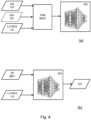
- FIG. 4(a) is a flow diagram of a proposed training phase of such a method.
- Dense AEI overlay data AEI OV and low resolution layout data LO RED LD e.g., pattern density data is used to train a machine learning model TRN MOD.
- dense ADI overlay data ADI OV may also be provided.
- the training may comprise training the model to interpolate or densify sparse sampling of the ADI metrology data or AEI metrology data using the low resolution layout data LO RED LD, such that the densified (modeled) data resembles the actual densely sampled metrology data (e.g., as close to within a threshold difference).
- the machine learning model may be a neural network or convolutional neural network (CNN).
- the pattern density data may comprise numerous (e.g., on the order of thousands) of cropped images of pattern density maps labeled by their relative measured overlay values.
- the measured overlay value may relate to overlay at a common point within all the images, e.g., overlay at the center of each image.
- the overlay may be measured via AEI metrology using a scatterometer or SEM for example.
- the method may be repeated for various mask designs (i.e., pattern density maps), such that the CNN is trained to be able to directly regress sparse overlay data, a pattern density image and wafer coordinate to the expected overlay values.
- mask designs i.e., pattern density maps
- the training step TRN MOD may comprise beginning training using pattern density maps covering a small area (small window), and increasing stepwise the area of the pattern density map used to train the neural network until the modeling accuracy saturates; i.e., there is no longer any (significant) improvement in modeling accuracy. That will indicate that long-range pattern density effect is correctly taken into account.
- FIG. 4(b) is a flow diagram illustrating an inference phase or production phase of the proposed method.
- sparse metrology data e.g., ADI or AEI metrology data
- SP MET at a small number of locations (e.g., such that in-line per-wafer metrology is feasible)
- low resolution layout data LO RED LD e.g., pattern density data for the structures being exposed
- the trained model regresses this sparse metrology data and low resolution layout data to overlay values OV over a field and/or the wafer.
- the model can be used to generate dense field or wafer overlay maps based on inputting sparse overlay data and a pattern density map, where an overlay map may comprise a spatial distribution of overlay vectors across the field/substrate, each vector having a direction of the overlay and a magnitude of the overlay. Overlay can then be estimated for any wafer coordinate based on the overlay map.
- the predicted full wafer overlay map may be used to optimize exposure setting for improving on-product overlay performance of the entire field or certain critical areas/features.
- the proposed method enables the use of a trained neural network and a few sparsely sampled overlay values to predict the high resolution full wafer overlay map, thereby providing a high accuracy densification of overlay data across wafer. In this way, per-wafer correction is possible.
- an embodiment may include a computer program containing one or more sequences of machine-readable instructions for causing the processors of the lithographic manufacturing system to implement methods of model mapping and control as described above.
- This computer program may be executed for example in a separate computer system employed for the image calculation/control process.
- the calculation steps may be wholly or partly performed within a processor a metrology tool, and/or the control unit LACU and/or supervisory control system SCS of Figures 1 and 2 .
- a data storage medium e.g., semiconductor memory, magnetic or optical disk having such a computer program stored therein in non-transient form.
- topography in a patterning device defines the pattern created on a substrate.
- the topography of the patterning device may be pressed into a layer of resist supplied to the substrate whereupon the resist is cured by applying electromagnetic radiation, heat, pressure or a combination thereof.
- the patterning device is moved out of the resist leaving a pattern in it after the resist is cured.
Landscapes
- Engineering & Computer Science (AREA)
- Physics & Mathematics (AREA)
- General Physics & Mathematics (AREA)
- Artificial Intelligence (AREA)
- Theoretical Computer Science (AREA)
- Evolutionary Computation (AREA)
- Health & Medical Sciences (AREA)
- Software Systems (AREA)
- Biomedical Technology (AREA)
- Life Sciences & Earth Sciences (AREA)
- Medical Informatics (AREA)
- Biophysics (AREA)
- Computational Linguistics (AREA)
- Data Mining & Analysis (AREA)
- General Health & Medical Sciences (AREA)
- Molecular Biology (AREA)
- Computing Systems (AREA)
- General Engineering & Computer Science (AREA)
- Mathematical Physics (AREA)
- Computer Vision & Pattern Recognition (AREA)
- Exposure And Positioning Against Photoresist Photosensitive Materials (AREA)
Priority Applications (3)
| Application Number | Priority Date | Filing Date | Title |
|---|---|---|---|
| EP22157745.5A EP4231096A1 (fr) | 2022-02-21 | 2022-02-21 | Procédés de métrologie |
| PCT/EP2023/051522 WO2023156143A1 (fr) | 2022-02-21 | 2023-01-23 | Procédés de métrologie |
| TW112105688A TW202347042A (zh) | 2022-02-21 | 2023-02-17 | 度量衡方法及其相關聯裝置 |
Applications Claiming Priority (1)
| Application Number | Priority Date | Filing Date | Title |
|---|---|---|---|
| EP22157745.5A EP4231096A1 (fr) | 2022-02-21 | 2022-02-21 | Procédés de métrologie |
Publications (1)
| Publication Number | Publication Date |
|---|---|
| EP4231096A1 true EP4231096A1 (fr) | 2023-08-23 |
Family
ID=80446108
Family Applications (1)
| Application Number | Title | Priority Date | Filing Date |
|---|---|---|---|
| EP22157745.5A Pending EP4231096A1 (fr) | 2022-02-21 | 2022-02-21 | Procédés de métrologie |
Country Status (1)
| Country | Link |
|---|---|
| EP (1) | EP4231096A1 (fr) |
Citations (5)
| Publication number | Priority date | Publication date | Assignee | Title |
|---|---|---|---|---|
| WO2019120826A1 (fr) * | 2017-12-19 | 2019-06-27 | Asml Netherlands B.V. | Correction et régulation utilisant la métrologie informatique |
| US20190228522A1 (en) * | 2018-01-22 | 2019-07-25 | Hitachi High-Technologies Corporation | Image Evaluation Method and Image Evaluation Device |
| EP3654103A1 (fr) * | 2018-11-14 | 2020-05-20 | ASML Netherlands B.V. | Procédé d'obtention de données d'apprentissage pour l'apprentissage d'un modèle d'un processus de fabrication de semi-conducteur |
| WO2021032376A1 (fr) * | 2019-08-20 | 2021-02-25 | Asml Netherlands B.V. | Procédé de commande d'un processus de fabrication de semi-conducteurs |
| US10990018B2 (en) | 2017-02-22 | 2021-04-27 | Asml Netherlands B.V. | Computational metrology |
-
2022
- 2022-02-21 EP EP22157745.5A patent/EP4231096A1/fr active Pending
Patent Citations (5)
| Publication number | Priority date | Publication date | Assignee | Title |
|---|---|---|---|---|
| US10990018B2 (en) | 2017-02-22 | 2021-04-27 | Asml Netherlands B.V. | Computational metrology |
| WO2019120826A1 (fr) * | 2017-12-19 | 2019-06-27 | Asml Netherlands B.V. | Correction et régulation utilisant la métrologie informatique |
| US20190228522A1 (en) * | 2018-01-22 | 2019-07-25 | Hitachi High-Technologies Corporation | Image Evaluation Method and Image Evaluation Device |
| EP3654103A1 (fr) * | 2018-11-14 | 2020-05-20 | ASML Netherlands B.V. | Procédé d'obtention de données d'apprentissage pour l'apprentissage d'un modèle d'un processus de fabrication de semi-conducteur |
| WO2021032376A1 (fr) * | 2019-08-20 | 2021-02-25 | Asml Netherlands B.V. | Procédé de commande d'un processus de fabrication de semi-conducteurs |
Similar Documents
| Publication | Publication Date | Title |
|---|---|---|
| US11493851B2 (en) | Lithographic method and lithographic apparatus | |
| US10444632B2 (en) | Apparatus operable to perform a measurement operation on a substrate, lithographic apparatus, and method of performing a measurement operation on a substrate | |
| US10725372B2 (en) | Method and apparatus for reticle optimization | |
| US10025193B2 (en) | Lithographic apparatus, device manufacturing method and associated data processing apparatus and computer program product | |
| KR20180064500A (ko) | 리소그래피 장치의 제어 방법 및 디바이스의 제조 방법, 리소그래피 장치를 위한 제어 시스템 및 리소그래피 장치 | |
| EP3312672A1 (fr) | Procédés de détermination de corrections pour un processus de formation de motif, procédé de fabrication de dispositif, système de commande pour un appareil lithographique et appareil lithographique | |
| US20190041758A1 (en) | Methods of determining a mechanical property of a layer applied to a substrate, control system for a lithographic apparatus and lithographic apparatus | |
| TWI833388B (zh) | 判定效能參數分布及/或相關聯分位數函數之方法以及相關聯電腦程式 | |
| KR102353128B1 (ko) | 기판 내의 응력을 결정하는 방법들, 리소그래피 공정을 제어하는 제어 시스템, 리소그래피 장치 및 컴퓨터 프로그램 제품 | |
| EP4231096A1 (fr) | Procédés de métrologie | |
| CN111480119B (zh) | 用于控制制造设备的方法以及相关联的设备 | |
| WO2019162203A1 (fr) | Procédé de détermination d'une valeur de paramètre dimensionnel corrigée relative à une caractéristique formée par un processus lithographique et appareils associés | |
| TWI811952B (zh) | 度量衡方法及設備 | |
| TWI841450B (zh) | 度量衡方法及設備 | |
| WO2023156143A1 (fr) | Procédés de métrologie | |
| EP4030236A1 (fr) | Procédé de surveillance d'un processus lithographique et appareils associés | |
| EP4202551A1 (fr) | Procédés de détermination d'une propriété mécanique d'une couche appliquée sur un substrat, et dispositifs associés | |
| EP4261617A1 (fr) | Procédés de métrologie et dispositifs associés | |
| WO2023198381A1 (fr) | Procédés de métrologie et dispositifs associés | |
| WO2023104391A1 (fr) | Procédés pour déterminer une propriété mécanique d'une couche appliquée sur un substrat, et dispositifs associés | |
| WO2024046691A1 (fr) | Procédé de configuration d'un champ de vision d'un appareil d'inspection | |
| KR20240056509A (ko) | 리소그래피 공정을 모니터링하는 방법 및 관련된 장치 | |
| TW202232620A (zh) | 監控微影製程之方法及相關裝置 | |
| WO2024052057A1 (fr) | Procédé de surveillance du bon fonctionnement d'un ou de plusieurs composants d'un système de lithographie | |
| WO2021151565A1 (fr) | Procédé de métrologie, métrologie associée et appareils lithographiques associés |
Legal Events
| Date | Code | Title | Description |
|---|---|---|---|
| PUAI | Public reference made under article 153(3) epc to a published international application that has entered the european phase |
Free format text: ORIGINAL CODE: 0009012 |
|
| STAA | Information on the status of an ep patent application or granted ep patent |
Free format text: STATUS: THE APPLICATION HAS BEEN PUBLISHED |
|
| AK | Designated contracting states |
Kind code of ref document: A1 Designated state(s): AL AT BE BG CH CY CZ DE DK EE ES FI FR GB GR HR HU IE IS IT LI LT LU LV MC MK MT NL NO PL PT RO RS SE SI SK SM TR |