EP4224157A1 - Électrode - Google Patents
Électrode Download PDFInfo
- Publication number
- EP4224157A1 EP4224157A1 EP21875403.4A EP21875403A EP4224157A1 EP 4224157 A1 EP4224157 A1 EP 4224157A1 EP 21875403 A EP21875403 A EP 21875403A EP 4224157 A1 EP4224157 A1 EP 4224157A1
- Authority
- EP
- European Patent Office
- Prior art keywords
- conductive carbon
- carbon layer
- electrode
- metal
- thickness direction
- Prior art date
- Legal status (The legal status is an assumption and is not a legal conclusion. Google has not performed a legal analysis and makes no representation as to the accuracy of the status listed.)
- Pending
Links
- OKTJSMMVPCPJKN-UHFFFAOYSA-N Carbon Chemical compound [C] OKTJSMMVPCPJKN-UHFFFAOYSA-N 0.000 claims abstract description 119
- 229910052799 carbon Inorganic materials 0.000 claims abstract description 118
- 229910052751 metal Inorganic materials 0.000 claims abstract description 64
- 239000002184 metal Substances 0.000 claims abstract description 64
- 229920005989 resin Polymers 0.000 claims abstract description 44
- 239000011347 resin Substances 0.000 claims abstract description 44
- 239000010936 titanium Substances 0.000 claims description 27
- RTAQQCXQSZGOHL-UHFFFAOYSA-N Titanium Chemical compound [Ti] RTAQQCXQSZGOHL-UHFFFAOYSA-N 0.000 claims description 26
- 229910052719 titanium Inorganic materials 0.000 claims description 26
- 238000002848 electrochemical method Methods 0.000 claims description 11
- 238000004544 sputter deposition Methods 0.000 description 36
- 238000000034 method Methods 0.000 description 31
- 230000007423 decrease Effects 0.000 description 14
- 238000005259 measurement Methods 0.000 description 13
- 230000000694 effects Effects 0.000 description 11
- 229920000139 polyethylene terephthalate Polymers 0.000 description 11
- 239000005020 polyethylene terephthalate Substances 0.000 description 11
- WCUXLLCKKVVCTQ-UHFFFAOYSA-M Potassium chloride Chemical compound [Cl-].[K+] WCUXLLCKKVVCTQ-UHFFFAOYSA-M 0.000 description 10
- 230000000052 comparative effect Effects 0.000 description 9
- YAGKRVSRTSUGEY-UHFFFAOYSA-N ferricyanide Chemical compound [Fe+3].N#[C-].N#[C-].N#[C-].N#[C-].N#[C-].N#[C-] YAGKRVSRTSUGEY-UHFFFAOYSA-N 0.000 description 8
- 239000007789 gas Substances 0.000 description 8
- 238000000168 high power impulse magnetron sputter deposition Methods 0.000 description 8
- 238000002484 cyclic voltammetry Methods 0.000 description 7
- XKRFYHLGVUSROY-UHFFFAOYSA-N Argon Chemical compound [Ar] XKRFYHLGVUSROY-UHFFFAOYSA-N 0.000 description 6
- 238000004458 analytical method Methods 0.000 description 6
- 238000005240 physical vapour deposition Methods 0.000 description 6
- -1 polyethylene terephthalate Polymers 0.000 description 6
- 239000001103 potassium chloride Substances 0.000 description 5
- 235000011164 potassium chloride Nutrition 0.000 description 5
- 230000001629 suppression Effects 0.000 description 5
- KDLHZDBZIXYQEI-UHFFFAOYSA-N Palladium Chemical compound [Pd] KDLHZDBZIXYQEI-UHFFFAOYSA-N 0.000 description 4
- 230000015572 biosynthetic process Effects 0.000 description 4
- 239000008280 blood Substances 0.000 description 4
- 210000004369 blood Anatomy 0.000 description 4
- 239000000463 material Substances 0.000 description 4
- 229920001225 polyester resin Polymers 0.000 description 4
- 239000004645 polyester resin Substances 0.000 description 4
- WQZGKKKJIJFFOK-GASJEMHNSA-N Glucose Natural products OC[C@H]1OC(O)[C@H](O)[C@@H](O)[C@@H]1O WQZGKKKJIJFFOK-GASJEMHNSA-N 0.000 description 3
- 238000000560 X-ray reflectometry Methods 0.000 description 3
- 229910052786 argon Inorganic materials 0.000 description 3
- 238000000151 deposition Methods 0.000 description 3
- 230000008021 deposition Effects 0.000 description 3
- 238000011156 evaluation Methods 0.000 description 3
- 239000008103 glucose Substances 0.000 description 3
- 230000033116 oxidation-reduction process Effects 0.000 description 3
- 238000009681 x-ray fluorescence measurement Methods 0.000 description 3
- VYZAMTAEIAYCRO-UHFFFAOYSA-N Chromium Chemical compound [Cr] VYZAMTAEIAYCRO-UHFFFAOYSA-N 0.000 description 2
- RYGMFSIKBFXOCR-UHFFFAOYSA-N Copper Chemical compound [Cu] RYGMFSIKBFXOCR-UHFFFAOYSA-N 0.000 description 2
- ZOKXTWBITQBERF-UHFFFAOYSA-N Molybdenum Chemical compound [Mo] ZOKXTWBITQBERF-UHFFFAOYSA-N 0.000 description 2
- XUIMIQQOPSSXEZ-UHFFFAOYSA-N Silicon Chemical compound [Si] XUIMIQQOPSSXEZ-UHFFFAOYSA-N 0.000 description 2
- BQCADISMDOOEFD-UHFFFAOYSA-N Silver Chemical compound [Ag] BQCADISMDOOEFD-UHFFFAOYSA-N 0.000 description 2
- 229910021607 Silver chloride Inorganic materials 0.000 description 2
- 229910045601 alloy Inorganic materials 0.000 description 2
- 239000000956 alloy Substances 0.000 description 2
- 229910052782 aluminium Inorganic materials 0.000 description 2
- XAGFODPZIPBFFR-UHFFFAOYSA-N aluminium Chemical compound [Al] XAGFODPZIPBFFR-UHFFFAOYSA-N 0.000 description 2
- 238000005229 chemical vapour deposition Methods 0.000 description 2
- 229910052804 chromium Inorganic materials 0.000 description 2
- 239000011651 chromium Substances 0.000 description 2
- 229910052802 copper Inorganic materials 0.000 description 2
- 239000010949 copper Substances 0.000 description 2
- PCHJSUWPFVWCPO-UHFFFAOYSA-N gold Chemical compound [Au] PCHJSUWPFVWCPO-UHFFFAOYSA-N 0.000 description 2
- 229910052737 gold Inorganic materials 0.000 description 2
- 239000010931 gold Substances 0.000 description 2
- 229910052734 helium Inorganic materials 0.000 description 2
- 239000001307 helium Substances 0.000 description 2
- SWQJXJOGLNCZEY-UHFFFAOYSA-N helium atom Chemical compound [He] SWQJXJOGLNCZEY-UHFFFAOYSA-N 0.000 description 2
- 229910052743 krypton Inorganic materials 0.000 description 2
- DNNSSWSSYDEUBZ-UHFFFAOYSA-N krypton atom Chemical compound [Kr] DNNSSWSSYDEUBZ-UHFFFAOYSA-N 0.000 description 2
- 238000001755 magnetron sputter deposition Methods 0.000 description 2
- 229910052750 molybdenum Inorganic materials 0.000 description 2
- 239000011733 molybdenum Substances 0.000 description 2
- 230000003287 optical effect Effects 0.000 description 2
- 229910052763 palladium Inorganic materials 0.000 description 2
- 229920005672 polyolefin resin Polymers 0.000 description 2
- 239000000843 powder Substances 0.000 description 2
- 229910052704 radon Inorganic materials 0.000 description 2
- SYUHGPGVQRZVTB-UHFFFAOYSA-N radon atom Chemical compound [Rn] SYUHGPGVQRZVTB-UHFFFAOYSA-N 0.000 description 2
- 229910052710 silicon Inorganic materials 0.000 description 2
- 239000010703 silicon Substances 0.000 description 2
- 229910052709 silver Inorganic materials 0.000 description 2
- 239000004332 silver Substances 0.000 description 2
- HKZLPVFGJNLROG-UHFFFAOYSA-M silver monochloride Chemical compound [Cl-].[Ag+] HKZLPVFGJNLROG-UHFFFAOYSA-M 0.000 description 2
- 239000000758 substrate Substances 0.000 description 2
- 229910052715 tantalum Inorganic materials 0.000 description 2
- GUVRBAGPIYLISA-UHFFFAOYSA-N tantalum atom Chemical compound [Ta] GUVRBAGPIYLISA-UHFFFAOYSA-N 0.000 description 2
- 239000013076 target substance Substances 0.000 description 2
- WFKWXMTUELFFGS-UHFFFAOYSA-N tungsten Chemical compound [W] WFKWXMTUELFFGS-UHFFFAOYSA-N 0.000 description 2
- 229910052721 tungsten Inorganic materials 0.000 description 2
- 239000010937 tungsten Substances 0.000 description 2
- 238000007740 vapor deposition Methods 0.000 description 2
- 229910052724 xenon Inorganic materials 0.000 description 2
- FHNFHKCVQCLJFQ-UHFFFAOYSA-N xenon atom Chemical compound [Xe] FHNFHKCVQCLJFQ-UHFFFAOYSA-N 0.000 description 2
- QTBSBXVTEAMEQO-UHFFFAOYSA-M Acetate Chemical compound CC([O-])=O QTBSBXVTEAMEQO-UHFFFAOYSA-M 0.000 description 1
- 239000004925 Acrylic resin Substances 0.000 description 1
- 229920000178 Acrylic resin Polymers 0.000 description 1
- 239000004695 Polyether sulfone Substances 0.000 description 1
- 239000004734 Polyphenylene sulfide Substances 0.000 description 1
- 239000004372 Polyvinyl alcohol Substances 0.000 description 1
- 229920001328 Polyvinylidene chloride Polymers 0.000 description 1
- 150000001925 cycloalkenes Chemical class 0.000 description 1
- 229910003460 diamond Chemical group 0.000 description 1
- 239000010432 diamond Chemical group 0.000 description 1
- 238000007733 ion plating Methods 0.000 description 1
- 238000001659 ion-beam spectroscopy Methods 0.000 description 1
- 238000004519 manufacturing process Methods 0.000 description 1
- 238000012986 modification Methods 0.000 description 1
- 230000004048 modification Effects 0.000 description 1
- 230000000704 physical effect Effects 0.000 description 1
- 229920003207 poly(ethylene-2,6-naphthalate) Polymers 0.000 description 1
- 229920006122 polyamide resin Polymers 0.000 description 1
- 229920001230 polyarylate Polymers 0.000 description 1
- 229920005668 polycarbonate resin Polymers 0.000 description 1
- 239000004431 polycarbonate resin Substances 0.000 description 1
- 229920006393 polyether sulfone Polymers 0.000 description 1
- 239000011112 polyethylene naphthalate Substances 0.000 description 1
- 229920001721 polyimide Polymers 0.000 description 1
- 239000009719 polyimide resin Substances 0.000 description 1
- 229920000069 polyphenylene sulfide Polymers 0.000 description 1
- 229920005990 polystyrene resin Polymers 0.000 description 1
- 229920002451 polyvinyl alcohol Polymers 0.000 description 1
- 239000004800 polyvinyl chloride Substances 0.000 description 1
- 229920000915 polyvinyl chloride Polymers 0.000 description 1
- 239000005033 polyvinylidene chloride Substances 0.000 description 1
- 238000001552 radio frequency sputter deposition Methods 0.000 description 1
- 238000005014 resonance ionization mass spectroscopy Methods 0.000 description 1
- 238000001004 secondary ion mass spectrometry Methods 0.000 description 1
- 230000035945 sensitivity Effects 0.000 description 1
- 238000005478 sputtering type Methods 0.000 description 1
- 230000003746 surface roughness Effects 0.000 description 1
- 238000001771 vacuum deposition Methods 0.000 description 1
- 238000004876 x-ray fluorescence Methods 0.000 description 1
Images
Classifications
-
- G—PHYSICS
- G01—MEASURING; TESTING
- G01N—INVESTIGATING OR ANALYSING MATERIALS BY DETERMINING THEIR CHEMICAL OR PHYSICAL PROPERTIES
- G01N27/00—Investigating or analysing materials by the use of electric, electrochemical, or magnetic means
- G01N27/26—Investigating or analysing materials by the use of electric, electrochemical, or magnetic means by investigating electrochemical variables; by using electrolysis or electrophoresis
- G01N27/28—Electrolytic cell components
- G01N27/30—Electrodes, e.g. test electrodes; Half-cells
- G01N27/308—Electrodes, e.g. test electrodes; Half-cells at least partially made of carbon
Definitions
- the present invention relates to an electrode.
- Patent Document 1 There has been known an electrode including a flexible substrate, a metal layer, and a conductive carbon layer in sequence in the thickness direction (ref: for example, Patent Document 1).
- Patent Document 1 describes in the electrode, noise is suppressed by setting the surface roughness of the conductive carbon layer to 2.0 nm or less.
- Patent Document 1 Japanese Unexamined Patent Publication No. 2019-105637
- the present invention provides an electrode capable of suppressing noise and suppressing a decrease in the signal intensity.
- the present invention (1) includes an electrode including a resin film, a metal underlayer, and a conductive carbon layer in sequence in a thickness direction, in which a surface of the conductive carbon layer has an arithmetic average roughness Ra of 1.50 nm or less and a skewness Rsk of 0.00 or more.
- the present invention (2) includes the electrode described in (1), in which the conductive carbon layer contains metal, and the metal is in a proportion of 5% by mass or more and 50% by mass or less relative to the conductive carbon layer.
- the present invention (3) includes the electrode described in (1) or (2), in which the metal is titanium.
- the present invention (4) includes the electrode described in any one of the above-described (1) to (3), being an electrode for electrochemical measurement.
- the surface of the conductive carbon layer has an arithmetic average roughness Ra of 1.50 or less and a skewness Rsk of 0.00 or more, so that it is possible to suppress noise and also suppress a decrease in the signal intensity.
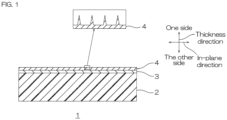
- FIG. 1 is a cross-sectional view of one embodiment of an electrode of the present invention.
- FIG. 1 One embodiment of the electrode of the present invention will be described with reference to FIG. 1 .
- an electrode 1 has a thickness.
- the electrode 1 has a film shape (including a sheet shape).
- the electrode 1 includes a resin film 2, a metal underlayer 3, and a conductive carbon layer 4 in sequence toward one side in the thickness direction.
- the electrode 1 preferably only includes the resin film 2, the metal underlayer 3, and the conductive carbon layer 4.
- the resin film 2 has a thickness.
- the resin film 2 is a substrate film in the electrode 1.
- the material of the resin film 2 is a resin.
- the resin include a polyester resin, an olefin resin, an acetate resin, a polyether sulfone resin, a polycarbonate resin, a polyamide resin, a polyimide resin, a polyolefin resin, an acrylic resin, a polyvinyl chloride resin, a polyvinylidene chloride resin, a polystyrene resin, a polyvinyl alcohol resin, a polyarylate resin, and a polyphenylene sulfide resin. These can be used alone or in combination.
- a polyester resin is used.
- the polyester resin include polyethylene terephthalate (PET) and polyethylene naphthalate.
- PET is used.
- the thickness of the resin film 2 is not particularly limited.
- the thickness of the resin film 2 is, for example, 2 ⁇ m or more, preferably 20 ⁇ m or more, and for example, 1000 ⁇ m or less, preferably 500 ⁇ m or less.
- An arithmetic average roughness Ra of one surface in the thickness direction of the resin film 2 is not particularly limited.
- the arithmetic average roughness Ra of the one surface in the thickness direction of the resin film 2 is, for example, 5 nm or less, preferably 1 nm or less, and for example, 0.1 nm or more, preferably 0.3 nm or more.
- the arithmetic average roughness Ra of the one surface in the thickness direction of the resin film 2 is measured in accordance with JIS B0601:2013.
- the arithmetic average roughness Ra of the following layers are measured in the same manner as above.
- a skewness Rsk of the one surface in the thickness direction of the resin film 2 is not particularly limited.
- the skewness Rsk of the one surface in the thickness direction of the resin film 2 is, for example, -0.3 or more, preferably -0.2 or more, and for example, 1.5 or less, preferably 0.8 or less.
- the skewness Rsk of the one surface in the thickness direction of the resin film 2 is determined as skewness of a roughness curve in accordance with JIS B0601:2013.
- the skewness Rsk of the following layers are measured in the same manner as above.
- the metal underlayer 3 is disposed on the one surface in the thickness direction of the resin film 2. Specifically, the metal underlayer 3 is in contact with the entire one surface in the thickness direction of the resin film 2.
- the metal underlayer 3 has a thickness.
- the material of the metal underlayer 3 is a metal.
- the metal include titanium, chromium, tungsten, aluminum, copper, silver, gold, molybdenum, tantalum, palladium, silicon, and alloys thereof.
- titanium preferably, titanium is used.
- the thickness of the metal underlayer 3 is not particularly limited.
- the thickness of the metal underlayer 3 is, for example, 1 nm or more, preferably 3 nm or more, more preferably 5 nm or more, and for example, 1000 nm or less, preferably 100 nm or less, more preferably 50 nm or less.
- the conductive carbon layer 4 is disposed on one surface in the thickness direction of the metal underlayer 3. Specifically, the conductive carbon layer 4 is in contact with the entire one surface in the thickness direction of the metal underlayer 3.
- the conductive carbon layer 4 has a thickness.
- the material of the conductive carbon layer 4 is mainly carbon.
- the carbon has, for example, an sp 2 bond and an sp 3 bond.
- Such carbon has a graphite structure and a diamond structure.
- the conductive carbon layer 4 can further contain a metal.
- the conductive carbon layer 4 further contains a metal, it is possible to further suppress noise and also further suppress a decrease in the signal intensity.
- the metal in the conductive carbon layer 4 may be the same as or different from the metal in the metal underlayer 3.
- the metal in the conductive carbon layer 4 is the same as in the metal underlayer 3.
- the metal examples include titanium, chromium, tungsten, aluminum, copper, silver, gold, molybdenum, tantalum, palladium, silicon, and alloys thereof.
- titanium is used.
- the metal is titanium, it is possible to further enhance adhesion between the conductive carbon layer 4 and the metal underlying layer 3.
- the metal is in a proportion of, for example, 0.1% by mass or more, preferably 1% by mass or more, more preferably 5% by mass or more, and for example, 50% by mass or less, preferably 35% by mass or less, even more preferably 20% by mass or less relative to the conductive carbon layer 4.
- the proportion of the metal in the conductive carbon layer 4 is the above-described lower limit or more and the above-described upper limit or less, it is possible to further suppress noise and also further suppress a decrease in the signal intensity.
- the presence or absence of and the proportion of the metal in the conductive carbon layer 4 are determined by X-ray fluorescence measurement.
- the conductive carbon layer 4 may further contain a rare gas.
- the rare gas include helium, argon, krypton, xenon, and radon.
- Examples of a method for analyzing the rare gas in the conductive carbon layer 4 include secondary ion mass spectrometry, resonance ionization mass spectrometry, and X-ray fluorescence analysis.
- a surface resistance value of one surface in the thickness direction of the conductive carbon layer 4 is not particularly limited.
- the surface resistance value of the one surface in the thickness direction of the conductive carbon layer 4 is, for example, 1.0 ⁇ 10 4 ⁇ / ⁇ or less, preferably 1.0 ⁇ 10 3 ⁇ / ⁇ or less.
- the surface resistance is measured by a four-terminal method in accordance with JIS K7194.
- the thickness of the conductive carbon layer 4 is not particularly limited.
- the thickness of the conductive carbon layer 4 is, for example, 1 nm or more, preferably 2 nm or more, more preferably 5 nm or more, and for example, 100 nm or less, preferably 70 nm or less, more preferably 50 nm or less.
- an arithmetic average roughness Ra to be described later in the one surface in the thickness direction of the conductive carbon layer 4 can be easily set within a desired range.
- the thickness of the conductive carbon layer 4 is the above-described lower limit or more, a uniform film can be deposited in an in-plane direction.
- the in-plane direction is a direction orthogonal to the thickness direction.
- the thickness of the conductive carbon layer 4 is calculated by measuring X-ray reflectivity.
- the arithmetic average roughness Ra of the one surface in the thickness direction of the conductive carbon layer 4 is 1.50 nm or less.
- the one surface in the thickness direction of the conductive carbon layer 4 in this embodiment is synonymous with the surface of the conductive carbon layer 4.
- the arithmetic average roughness Ra of the one surface in the thickness direction of the conductive carbon layer 4 is preferably 1.25 nm or less, more preferably 1.00 nm or less, even more preferably 0.75 nm or less, particularly preferably 0.70 nm or less.
- a capacitance value becomes extremely high. This increases noise. That is, in the present embodiment, since the arithmetic average roughness Ra of the one surface in the thickness direction of the conductive carbon layer 4 is 1.50 nm or less, noise can be suppressed. For example, in the present embodiment, the capacitance value measured by cyclic voltammetry can be lowered, and therefore, the suppression of noise as described above is demonstrated (see the Examples section below). To set the arithmetic average roughness Ra of the one surface in the thickness direction of the conductive carbon layer 4 in the above-described range, for example, the thickness of the conductive carbon layer 4 is adjusted.
- the lower limit of the arithmetic average roughness Ra of the one surface in the thickness direction of the conductive carbon layer 4 is not particularly limited.
- the lower limit of the arithmetic average roughness Ra of the one surface in the thickness direction of the conductive carbon layer 4 is, for example, 0.01 nm, preferably 0.10 nm.
- the one surface in the thickness direction of the conductive carbon layer 4 has a skewness Rsk of 0.00 or more.
- the skewness Rsk of the one surface in the thickness direction of the conductive carbon layer 4 is preferably 0.15 or more, more preferably 0.20 or more.
- the signal intensity decreases. Specifically, when cyclic voltammetry is performed using the electrode 1, an oxidation-reduction potential difference ⁇ Ep increases. This decreases the signal intensity.
- the skewness Rsk of the one surface in the thickness direction of the conductive carbon layer 4 is 0.00 or more, it is possible to suppress a decrease in the signal intensity.
- a decrease in the signal intensity is suppressed as described above, because the oxidation-reduction potential difference ⁇ Ep (specifically, ferricyanide activity value) by cyclic voltammetry is low (see the Examples section below).
- ⁇ Ep specifically, ferricyanide activity value
- the one surface in the thickness direction of the conductive carbon layer 4 having a skewness Rsk of 0.00 or more indicates that the skewness Rsk is 0 or a positive integer. Then, protrusions in the one surface in the thickness direction of the conductive carbon layer 4 are steep and sparse. More specifically, spaces between the protrusions become wider, which in turn increases a proportion occupied by recessed portions. This allows a large amount of measurement target substance to be held in the recessed portions, and the measurement target substance can be measured with good sensitivity, so that it is presumed that a decrease in the signal intensity can be suppressed.
- the upper limit of the skewness Rsk of the one surface in the thickness direction of the conductive carbon layer 4 is not particularly limited.
- the upper limit of the skewness Rsk of the one surface in the thickness direction of the conductive carbon layer 4 is, for example, 1.50.
- the resin film 2 is prepared. Then, the metal underlayer 3 and the conductive carbon layer 4 are formed in sequence on one side in the thickness direction of the resin film 2.
- Examples of the method for forming the metal underlayer 3 include a dry method and a wet method.
- a dry method is used.
- Examples of the dry method include a physical vapor deposition (PVD) method and a chemical vapor deposition (CVD) method.
- PVD physical vapor deposition
- CVD chemical vapor deposition
- a PVD method is used.
- Examples of the PVD method include a sputtering method, a vacuum deposition method, a laser vapor deposition method, and an ion plating method (arc vapor deposition method).
- a sputtering method is used. The sputtering method is not particularly limited.
- Examples of the sputtering method include unbalanced magnetron sputtering (UBM sputtering), high power impulse magnetron sputtering, electron cyclotron resonance sputtering, RF sputtering, DC sputtering (DC magnetron sputtering), DC pulse sputtering, and ion beam sputtering.
- UBM sputtering unbalanced magnetron sputtering
- high power impulse magnetron sputtering high power impulse magnetron sputtering
- electron cyclotron resonance sputtering RF sputtering
- DC sputtering DC magnetron sputtering
- DC pulse sputtering DC pulse sputtering
- ion beam sputtering ion beam sputtering
- a sputtering gas and a target are used.
- the sputtering gas contains a rare gas.
- the rare gas include helium, argon, krypton, xenon, and radon.
- the target is made of the above-described metal.
- the pressure during sputtering is, for example, 0.01 Pa or more, and for example, 10 Pa or less.
- the same method as the above-described method for forming the metal underlayer 3 is used.
- a dry method is used, more preferably a PVD method is used, even more preferably a sputtering method is used, particularly preferably a high power impulse magnetron sputtering method and a DC pulse sputtering method are used.
- the target for example, carbon is used, preferably sintered carbon is used.
- the conductive carbon layer 4 contains metal, carbon and metal are used as the target.
- a first target made of carbon (preferably, sintered carbon) and a second target made of metal (preferably, titanium) are used.
- each of the first target and the second target are disposed in one film deposition chamber independently of the other.
- the pulse width generally refers to a discharge stop period.
- the pulse width is, for example, 0.5 ⁇ s or more, and for example, 1 ms or less.
- the frequency is, for example, 10 kHz or more, and for example, 500 kHz or less.
- the pulse width generally refers to a discharge duration.
- the pulse width is, for example, 10 ⁇ s or more, and for example, 3 ms or less.
- the frequency is, for example, 50 Hz or more, and for example, 3 kHz or less.
- the electrode 1 including the resin film 2, the metal underlayer 3, and the conductive carbon layer 4 in sequence is produced.
- the one surface in the thickness direction of the conductive carbon layer 4 has an arithmetic average roughness Ra of 1.5 nm or less and a skewness Rsk of 0.0 or more. Therefore, it is possible to suppress noise and also suppress a decrease in the signal intensity.
- the conductive carbon layer 4 further contains metal and the metal is in a proportion of 5% by mass or more and 50% by mass or less relative to the conductive carbon layer 4, it is possible to further suppress noise and also further suppress a decrease in the signal intensity.
- the metal is titanium, it is possible to further enhance adhesion between the conductive carbon layer 4 and the metal underlying layer 3.
- the use of the electrode 1 is not particularly limited.
- Examples of the use of the electrode 1 include electrodes for electrochemical measurement.
- the electrode 1 is provided in an electrochemical measurement system as a working electrode.
- the electrode 1 is used as an electrode for electrochemical measurement.
- Using the electrochemical measurement system for example, cyclic voltammetry is performed.
- Examples of the use of the electrochemical measurement system include a blood glucose level sensor.
- the blood glucose level sensor measures blood glucose levels in blood.
- a modified electrode 1 can further include the metal underlayer 3 and the conductive carbon layer 4 disposed in sequence toward the other side in the thickness direction of the resin film 2.
- the conductive carbon layer 4, the metal underlayer 3, the resin film 2, the metal underlayer 3, and the conductive carbon layer 4 are disposed in sequence toward one side in the thickness direction.
- the other surface in the thickness direction of the conductive carbon layer 4 disposed on the other side in the thickness direction of the resin film 2 has an arithmetic average roughness Ra of 1.5 nm or less and a skewness Rsk of 0.0 or more.
- each of the one surface and the other surface in the thickness direction of the conductive carbon layer 4 is one example of the surface of the conductive carbon layer 4.
- a 50 ⁇ m-thick resin film 2 made of polyethylene terephthalate (PET) was prepared.
- One surface in the thickness direction of the resin film 2 had an arithmetic average roughness Ra of 0.6 nm.
- the one surface in the thickness direction of the resin film 2 had a skewness Rsk of -0.11.
- a metal underlayer 3 made of titanium was formed on the one surface in the thickness direction of the resin film 2 by a DC sputtering method.
- the metal underlayer 3 had a thickness of 7 nm.
- Conditions of the DC sputtering method are as follows.
- a conductive carbon layer 4 was formed on one surface in the thickness direction of the metal underlayer 3 by a DC pulse sputtering method. Conditions of the DC pulse sputtering method will be described below.
- the conductive carbon layer 4 contained 10% by mass of titanium.
- the content of the titanium was determined by X-ray fluorescence measurement.
- the resulting peak intensities of titanium were derived from both the titanium contained in the conductive carbon layer 4 and the titanium used for the metal underlying layer 3.
- a peak intensity of a sample on which a film of only the titanium of the metal underlying layer 3 was previously deposited under the same conditions as in the sputtering method of the conductive carbon layer 4 was subtracted from the peak of the conductive carbon layer 4, to thereby calculate the content of the titanium contained only in the conductive carbon layer 4.
- the thickness of the conductive carbon layer 4 was 10 nm. A method for measuring the thickness of the conductive carbon layer 4 will be described later.
- Example 2 The same treatment as in Example 1 was performed to produce the electrode 1.
- the DC pulse sputtering method was changed to a high power impulse magnetron sputtering method.
- the average electric power applied to the first target was set to 150 W, and electric power was not applied to the second target.
- the pulse width was changed to 30 ⁇ s, and the frequency was changed to 210 Hz.
- the pressure in the sputtering chamber was changed to 1.0 Pa.
- the conductive carbon layer 4 did not contain titanium and was substantially made of carbon.
- the thickness of the conductive carbon layer 4 was 35 nm.
- Example 2 The same treatment as in Example 1 was performed to produce the electrode 1. However, in the formation of the conductive carbon layer 4, electric power was not applied to the second target.
- the conductive carbon layer 4 did not contain titanium and was substantially made of carbon.
- Example 2 The same treatment as in Example 1 was performed to produce the electrode 1. However, in the formation of the conductive carbon layer 4, electric power was not applied to the second target.
- the conductive carbon layer 4 did not contain titanium and was substantially made of carbon.
- the thickness of the conductive carbon layer 4 was 100 nm.
- Example 2 The same treatment as in Example 1 was performed to produce the electrode 1.
- the DC pulse sputtering method was changed to a high power impulse magnetron sputtering method.
- the electric power applied to the first target was set to 150 W, and electric power was not applied to the second target.
- the pulse width was changed to 30 ⁇ s, and the frequency was changed to 210 Hz.
- the pressure in the sputtering chamber was changed to 0.6 Pa.
- the conductive carbon layer 4 did not contain titanium and was substantially made of carbon.
- the thickness of the conductive carbon layer 4 was 35 nm.
- Example 3 The same treatment as in Example 3 was performed to produce the electrode 1. However, the material of the resin film 2 was changed to cycloolefin resin (COP).
- COP cycloolefin resin
- the thickness of the conductive carbon layer 4 was calculated by measuring an X-ray reflectivity with a powder X-ray diffractometer ("RINT-2200", manufactured by Rigaku Corporation) under the following ⁇ measurement conditions> and then analyzing the obtained measurement data with an analytics software ("GXRR3", manufactured by Rigaku Corporation).
- RINT-2200 powder X-ray diffractometer
- GXRR3 analytics software
- a three-layer model including the resin film 2 made of PET, the metal underlayer 3 made of titanium, and the conductive carbon layer 4 made of titanium was adopted under the following ⁇ analysis conditions>.
- the targeted thickness of the metal underlayer 3, the arithmetic average roughness Ra of 0.5 nm, and the density of 4.51 g/cm 3 were input as initial values.
- the targeted thickness of the conductive carbon layer 4, the arithmetic average roughness Ra of 0.5 nm, and the density of 1.95 g/cm 3 were input as initial values. Thereafter, least square fitting with the measured values was performed, thereby analyzing the thickness of the conductive carbon layer 4.
- the electrode was fabricated as a working electrode.
- the working electrode was inserted into a potassium chloride solution in which K 4 [Fe(CN) 6 ] was dissolved, and was connected to a potentiostat (pocketSTAT, manufactured by IVIUM).
- the solution had a potassium chloride concentration of 1.0 mol/L.
- the solution had a K 4 [Fe(CN) 6 ] concentration of 1.0 mol/L.
- a reference electrode (Ag/AgCl) and a counter electrode (Pt) were inserted into the potassium chloride solution and then connected to the potentiostat. Thereafter, cyclic voltammetry was performed in a potential range of from -0.1 V to 0.5 V at a scan rate of 0.1 V/sec. The oxidation-reduction potential difference ⁇ Ep was acquired as a ferricyanide activity value.
- the ferricyanide activity value was applied to the following criteria and the signal intensity of the electrode 1 was evaluated.
- the electrode was fabricated as a working electrode.
- the working electrode was inserted into a 1.0 mol/L potassium chloride solution, and was connected to a potentiostat (pocketSTAT, manufactured by IVIUM).
- a reference electrode Ag/AgCl
- a counter electrode Pt
- Capacitance value sum of absolute values of two current values at 0.25 V A / 2 ⁇ 0.01 V / sec / 0.0314 cm 2
- the unit of the capacitance value is [A]/[V/sec]/[cm 2 ], which is the same as [F/cm 2 ].
- the capacitance value was applied to the following criteria and the suppression of noise in the electrode 1 was evaluated.
- the electrode is used for electrochemical measurement.
Landscapes
- Chemical & Material Sciences (AREA)
- Life Sciences & Earth Sciences (AREA)
- Health & Medical Sciences (AREA)
- Biochemistry (AREA)
- Chemical Kinetics & Catalysis (AREA)
- Electrochemistry (AREA)
- Physics & Mathematics (AREA)
- Analytical Chemistry (AREA)
- Molecular Biology (AREA)
- General Health & Medical Sciences (AREA)
- General Physics & Mathematics (AREA)
- Immunology (AREA)
- Pathology (AREA)
- Cell Electrode Carriers And Collectors (AREA)
- Physical Vapour Deposition (AREA)
- Non-Insulated Conductors (AREA)
Applications Claiming Priority (2)
| Application Number | Priority Date | Filing Date | Title |
|---|---|---|---|
| JP2020165209 | 2020-09-30 | ||
| PCT/JP2021/035024 WO2022071101A1 (fr) | 2020-09-30 | 2021-09-24 | Électrode |
Publications (2)
| Publication Number | Publication Date |
|---|---|
| EP4224157A1 true EP4224157A1 (fr) | 2023-08-09 |
| EP4224157A4 EP4224157A4 (fr) | 2024-10-23 |
Family
ID=80950254
Family Applications (1)
| Application Number | Title | Priority Date | Filing Date |
|---|---|---|---|
| EP21875403.4A Pending EP4224157A4 (fr) | 2020-09-30 | 2021-09-24 | Électrode |
Country Status (6)
| Country | Link |
|---|---|
| US (1) | US20240019394A1 (fr) |
| EP (1) | EP4224157A4 (fr) |
| JP (1) | JPWO2022071101A1 (fr) |
| CN (1) | CN116457655A (fr) |
| TW (1) | TW202223383A (fr) |
| WO (1) | WO2022071101A1 (fr) |
Families Citing this family (1)
| Publication number | Priority date | Publication date | Assignee | Title |
|---|---|---|---|---|
| US20250012753A1 (en) * | 2021-09-30 | 2025-01-09 | Nitto Denko Corporation | Electrode |
Family Cites Families (5)
| Publication number | Priority date | Publication date | Assignee | Title |
|---|---|---|---|---|
| JP4992425B2 (ja) * | 2004-08-30 | 2012-08-08 | 三菱化学株式会社 | 非水系二次電池用負極材料、非水系二次電池用負極、および非水系二次電池 |
| WO2010004690A1 (fr) * | 2008-07-09 | 2010-01-14 | 日本電気株式会社 | Électrode de carbone, capteur électrochimique, et procédé de fabrication d'une électrode de carbone |
| US10156539B2 (en) * | 2016-08-22 | 2018-12-18 | King Fahd University Of Petroleum And Minerals | Graphite electrode comprising electrochemically reduced graphene oxide and methods thereof |
| JP7337498B2 (ja) | 2017-12-11 | 2023-09-04 | 日東電工株式会社 | 電極フィルムおよび電気化学測定システム |
| JP6752432B1 (ja) * | 2019-03-28 | 2020-09-09 | 日東電工株式会社 | 電極および電気化学測定システム |
-
2021
- 2021-09-24 WO PCT/JP2021/035024 patent/WO2022071101A1/fr active Application Filing
- 2021-09-24 CN CN202180066766.8A patent/CN116457655A/zh active Pending
- 2021-09-24 JP JP2022553891A patent/JPWO2022071101A1/ja active Pending
- 2021-09-24 EP EP21875403.4A patent/EP4224157A4/fr active Pending
- 2021-09-24 US US18/247,116 patent/US20240019394A1/en active Pending
- 2021-09-29 TW TW110136192A patent/TW202223383A/zh unknown
Also Published As
| Publication number | Publication date |
|---|---|
| US20240019394A1 (en) | 2024-01-18 |
| TW202223383A (zh) | 2022-06-16 |
| WO2022071101A1 (fr) | 2022-04-07 |
| JPWO2022071101A1 (fr) | 2022-04-07 |
| EP4224157A4 (fr) | 2024-10-23 |
| CN116457655A (zh) | 2023-07-18 |
Similar Documents
| Publication | Publication Date | Title |
|---|---|---|
| JP6810330B2 (ja) | 電極および電気化学測定システム | |
| EP2124278A1 (fr) | Séparateur de pile à combustible, procédé de séparation de pile à combustible et pile à combustible | |
| EP4130728A1 (fr) | Électrode | |
| EP2817430B1 (fr) | Revêtement présentant des caractéristiques de conduction et de résistance à la corrosion | |
| EP3951375A1 (fr) | Électrode et système de mesure électrochimique | |
| EP3726207A1 (fr) | Film d'électrode et système de mesure électrochimique | |
| EP4224157A1 (fr) | Électrode | |
| EP3512958B1 (fr) | Électrodes de biocapteur préparées par dépôt physique en phase vapeur | |
| KR100374782B1 (ko) | 전계 방출형 전자원 및 그 제조방법 | |
| US10509004B2 (en) | Sensor elements with a tantalum- or niobium-containing base layer and methods of producing the same | |
| JP6404069B2 (ja) | 合金ナノ粒子含有カーボン電極、当該電極を含む装置、及び、当該電極の製造方法 | |
| EP4317958A1 (fr) | Électrode | |
| US12159998B2 (en) | Electrode and electrochemical measurement system | |
| EP4502587A1 (fr) | Électrode et système de mesure électrochimique | |
| WO2022210387A1 (fr) | Électrode | |
| EP3303984B1 (fr) | Électrode de biocapteur et procédé de fabrication d'une électrode de biocapteur | |
| EP4317521A1 (fr) | Électrode, et son procédé de production | |
| TWI870396B (zh) | 電極及電化學測定系統 | |
| KR20130046637A (ko) | 바이오센서 | |
| EP4187239A1 (fr) | Électrode | |
| TW202438882A (zh) | 電極 |
Legal Events
| Date | Code | Title | Description |
|---|---|---|---|
| STAA | Information on the status of an ep patent application or granted ep patent |
Free format text: STATUS: THE INTERNATIONAL PUBLICATION HAS BEEN MADE |
|
| PUAI | Public reference made under article 153(3) epc to a published international application that has entered the european phase |
Free format text: ORIGINAL CODE: 0009012 |
|
| STAA | Information on the status of an ep patent application or granted ep patent |
Free format text: STATUS: REQUEST FOR EXAMINATION WAS MADE |
|
| 17P | Request for examination filed |
Effective date: 20230328 |
|
| AK | Designated contracting states |
Kind code of ref document: A1 Designated state(s): AL AT BE BG CH CY CZ DE DK EE ES FI FR GB GR HR HU IE IS IT LI LT LU LV MC MK MT NL NO PL PT RO RS SE SI SK SM TR |
|
| DAV | Request for validation of the european patent (deleted) | ||
| DAX | Request for extension of the european patent (deleted) | ||
| A4 | Supplementary search report drawn up and despatched |
Effective date: 20240924 |
|
| RIC1 | Information provided on ipc code assigned before grant |
Ipc: G01N 27/30 20060101AFI20240918BHEP |