EP4223209A1 - Endoscope - Google Patents
Endoscope Download PDFInfo
- Publication number
- EP4223209A1 EP4223209A1 EP22749407.7A EP22749407A EP4223209A1 EP 4223209 A1 EP4223209 A1 EP 4223209A1 EP 22749407 A EP22749407 A EP 22749407A EP 4223209 A1 EP4223209 A1 EP 4223209A1
- Authority
- EP
- European Patent Office
- Prior art keywords
- light emitting
- conductive portion
- substrate
- mounting substrate
- emitting elements
- Prior art date
- Legal status (The legal status is an assumption and is not a legal conclusion. Google has not performed a legal analysis and makes no representation as to the accuracy of the status listed.)
- Pending
Links
- 239000000758 substrate Substances 0.000 claims abstract description 135
- 230000002093 peripheral effect Effects 0.000 claims abstract description 43
- 238000003780 insertion Methods 0.000 claims abstract description 22
- 230000037431 insertion Effects 0.000 claims abstract description 22
- 238000005452 bending Methods 0.000 description 14
- 238000005286 illumination Methods 0.000 description 5
- 238000003384 imaging method Methods 0.000 description 5
- 238000009413 insulation Methods 0.000 description 4
- 239000004020 conductor Substances 0.000 description 2
- 238000010586 diagram Methods 0.000 description 2
- 230000003287 optical effect Effects 0.000 description 2
- 239000011347 resin Substances 0.000 description 2
- 229920005989 resin Polymers 0.000 description 2
- 239000004065 semiconductor Substances 0.000 description 2
- RYGMFSIKBFXOCR-UHFFFAOYSA-N Copper Chemical compound [Cu] RYGMFSIKBFXOCR-UHFFFAOYSA-N 0.000 description 1
- 229910000881 Cu alloy Inorganic materials 0.000 description 1
- 239000000853 adhesive Substances 0.000 description 1
- 230000001070 adhesive effect Effects 0.000 description 1
- 238000006243 chemical reaction Methods 0.000 description 1
- 230000000295 complement effect Effects 0.000 description 1
- 229910052802 copper Inorganic materials 0.000 description 1
- 239000010949 copper Substances 0.000 description 1
- 230000000694 effects Effects 0.000 description 1
- 239000002184 metal Substances 0.000 description 1
- 229910052751 metal Inorganic materials 0.000 description 1
- 229910044991 metal oxide Inorganic materials 0.000 description 1
- 150000004706 metal oxides Chemical class 0.000 description 1
- 238000012986 modification Methods 0.000 description 1
- 230000004048 modification Effects 0.000 description 1
- 238000000465 moulding Methods 0.000 description 1
- 238000007781 pre-processing Methods 0.000 description 1
- 239000002356 single layer Substances 0.000 description 1
Images



Classifications
-
- A—HUMAN NECESSITIES
- A61—MEDICAL OR VETERINARY SCIENCE; HYGIENE
- A61B—DIAGNOSIS; SURGERY; IDENTIFICATION
- A61B1/00—Instruments for performing medical examinations of the interior of cavities or tubes of the body by visual or photographical inspection, e.g. endoscopes; Illuminating arrangements therefor
- A61B1/06—Instruments for performing medical examinations of the interior of cavities or tubes of the body by visual or photographical inspection, e.g. endoscopes; Illuminating arrangements therefor with illuminating arrangements
- A61B1/0661—Endoscope light sources
- A61B1/0676—Endoscope light sources at distal tip of an endoscope
-
- A—HUMAN NECESSITIES
- A61—MEDICAL OR VETERINARY SCIENCE; HYGIENE
- A61B—DIAGNOSIS; SURGERY; IDENTIFICATION
- A61B1/00—Instruments for performing medical examinations of the interior of cavities or tubes of the body by visual or photographical inspection, e.g. endoscopes; Illuminating arrangements therefor
- A61B1/00002—Operational features of endoscopes
- A61B1/00011—Operational features of endoscopes characterised by signal transmission
- A61B1/00018—Operational features of endoscopes characterised by signal transmission using electrical cables
-
- A—HUMAN NECESSITIES
- A61—MEDICAL OR VETERINARY SCIENCE; HYGIENE
- A61B—DIAGNOSIS; SURGERY; IDENTIFICATION
- A61B1/00—Instruments for performing medical examinations of the interior of cavities or tubes of the body by visual or photographical inspection, e.g. endoscopes; Illuminating arrangements therefor
- A61B1/00002—Operational features of endoscopes
- A61B1/00025—Operational features of endoscopes characterised by power management
- A61B1/00027—Operational features of endoscopes characterised by power management characterised by power supply
-
- A—HUMAN NECESSITIES
- A61—MEDICAL OR VETERINARY SCIENCE; HYGIENE
- A61B—DIAGNOSIS; SURGERY; IDENTIFICATION
- A61B1/00—Instruments for performing medical examinations of the interior of cavities or tubes of the body by visual or photographical inspection, e.g. endoscopes; Illuminating arrangements therefor
- A61B1/00064—Constructional details of the endoscope body
- A61B1/00071—Insertion part of the endoscope body
- A61B1/0008—Insertion part of the endoscope body characterised by distal tip features
- A61B1/00096—Optical elements
-
- A—HUMAN NECESSITIES
- A61—MEDICAL OR VETERINARY SCIENCE; HYGIENE
- A61B—DIAGNOSIS; SURGERY; IDENTIFICATION
- A61B1/00—Instruments for performing medical examinations of the interior of cavities or tubes of the body by visual or photographical inspection, e.g. endoscopes; Illuminating arrangements therefor
- A61B1/00112—Connection or coupling means
- A61B1/00114—Electrical cables in or with an endoscope
-
- A—HUMAN NECESSITIES
- A61—MEDICAL OR VETERINARY SCIENCE; HYGIENE
- A61B—DIAGNOSIS; SURGERY; IDENTIFICATION
- A61B1/00—Instruments for performing medical examinations of the interior of cavities or tubes of the body by visual or photographical inspection, e.g. endoscopes; Illuminating arrangements therefor
- A61B1/04—Instruments for performing medical examinations of the interior of cavities or tubes of the body by visual or photographical inspection, e.g. endoscopes; Illuminating arrangements therefor combined with photographic or television appliances
- A61B1/05—Instruments for performing medical examinations of the interior of cavities or tubes of the body by visual or photographical inspection, e.g. endoscopes; Illuminating arrangements therefor combined with photographic or television appliances characterised by the image sensor, e.g. camera, being in the distal end portion
-
- A—HUMAN NECESSITIES
- A61—MEDICAL OR VETERINARY SCIENCE; HYGIENE
- A61B—DIAGNOSIS; SURGERY; IDENTIFICATION
- A61B1/00—Instruments for performing medical examinations of the interior of cavities or tubes of the body by visual or photographical inspection, e.g. endoscopes; Illuminating arrangements therefor
- A61B1/06—Instruments for performing medical examinations of the interior of cavities or tubes of the body by visual or photographical inspection, e.g. endoscopes; Illuminating arrangements therefor with illuminating arrangements
- A61B1/0607—Instruments for performing medical examinations of the interior of cavities or tubes of the body by visual or photographical inspection, e.g. endoscopes; Illuminating arrangements therefor with illuminating arrangements for annular illumination
-
- A—HUMAN NECESSITIES
- A61—MEDICAL OR VETERINARY SCIENCE; HYGIENE
- A61B—DIAGNOSIS; SURGERY; IDENTIFICATION
- A61B1/00—Instruments for performing medical examinations of the interior of cavities or tubes of the body by visual or photographical inspection, e.g. endoscopes; Illuminating arrangements therefor
- A61B1/06—Instruments for performing medical examinations of the interior of cavities or tubes of the body by visual or photographical inspection, e.g. endoscopes; Illuminating arrangements therefor with illuminating arrangements
- A61B1/0661—Endoscope light sources
- A61B1/0684—Endoscope light sources using light emitting diodes [LED]
-
- A—HUMAN NECESSITIES
- A61—MEDICAL OR VETERINARY SCIENCE; HYGIENE
- A61B—DIAGNOSIS; SURGERY; IDENTIFICATION
- A61B1/00—Instruments for performing medical examinations of the interior of cavities or tubes of the body by visual or photographical inspection, e.g. endoscopes; Illuminating arrangements therefor
- A61B1/12—Instruments for performing medical examinations of the interior of cavities or tubes of the body by visual or photographical inspection, e.g. endoscopes; Illuminating arrangements therefor with cooling or rinsing arrangements
- A61B1/128—Instruments for performing medical examinations of the interior of cavities or tubes of the body by visual or photographical inspection, e.g. endoscopes; Illuminating arrangements therefor with cooling or rinsing arrangements provided with means for regulating temperature
-
- G—PHYSICS
- G02—OPTICS
- G02B—OPTICAL ELEMENTS, SYSTEMS OR APPARATUS
- G02B23/00—Telescopes, e.g. binoculars; Periscopes; Instruments for viewing the inside of hollow bodies; Viewfinders; Optical aiming or sighting devices
- G02B23/24—Instruments or systems for viewing the inside of hollow bodies, e.g. fibrescopes
- G02B23/2407—Optical details
- G02B23/2461—Illumination
Definitions
- the present disclosure relates to an endoscope.
- An endoscope is a medical instrument to be inserted into a body cavity of a subject to observe and treat a desired site and includes an imaging unit provided in a distal end portion of an insertion tube to be inserted into the body cavity, and an illumination device illuminating an imaging field of view of the imaging unit.
- Patent Literature 1 discloses an endoscope including an illumination device for achieving illumination in a wide angular range of equal to or greater than 180 degrees to enable observation at a wide viewing angle.
- Patent Literature 1 JP 2015-16021 A
- an object is to provide an endoscope in which a conductive portion to which a power supply line for supplying power to a light emitting element is connected can be suitably arranged.
- An endoscope is an endoscope including a light emitting module incorporated in a distal end portion of an insertion tube, in which the light emitting module includes a mounting substrate on which a plurality of light emitting elements is mounted, the mounting substrate has an annular shape in which a hole through which an image sensor using the light emitting elements as a light source is to be inserted is provided in a central portion and includes a first surface on which the light emitting elements are surface-mounted and a side surface located at a peripheral edge of the first surface, a conductive portion electrically connected to the light emitting elements is provided on the side surface, and a power supply line for supplying power to the light emitting elements is connected to the conductive portion.
- an endoscope in which a conductive portion to which a power supply line for supplying power to a light emitting element is connected is suitably arranged.
- Fig. 1 is an external view of an endoscope 1 according to a first embodiment.
- the endoscope 1 includes an insertion tube 2, an operation unit 3, a universal tube 4, and a connector unit 5.
- the insertion tube 2 is a portion to be inserted into a body cavity and includes a long soft portion 20 and a distal end portion 22 connected to one end of the soft portion 20 via a bending section 21.
- the other end of the soft portion 20 is connected to the operation unit 3 via a cylindrical connection portion 23.
- the universal tube 4 has one end connected to the operation unit 3 and extends in a direction different from the insertion tube 2, and the connector unit 5 is connected to the other end of the universal tube 4.
- the operation unit 3 is provided to be gripped by a user (operator) of the endoscope 1 such as a doctor to perform various kinds of operation and includes a bending operation knob 30 and a plurality of operation buttons 31, and the like.
- the bending operation knob 30 is connected to the bending section 21 by a wire (not illustrated) passing through inside of each of the connection portion 23 and the soft portion 20.
- the bending section 21 is bent in two directions orthogonal to each other in an axial cross section through operation of the bending operation knob 30, thereby changing a direction of the distal end portion 22 inserted into a body cavity.
- the endoscope 1 is connected to a processor device 10 via the connector unit 5 and is used as an endoscope 1 device.
- the processor device 10 includes a control unit, a storage unit, a signal processing circuit, and the like, and integrally controls the endoscope device by a control program stored in the storage unit.
- Fig. 2 is an enlarged view of the distal end portion of the insertion tube.
- the distal end portion 22 includes a cylindrical housing 24 having one side fixed to the bending section 21.
- the other side of the housing 24 is covered with a central objective lens 25 and an annular light distribution lens 26 surrounding a periphery of the objective lens 25.
- An image sensor 6 is provided inside the housing 24 to face an inner side of the objective lens 25.
- the image sensor 6 captures an image of a subject to be observed (an object), which is a body part such as a body cavity, through the objective lens 25.
- the objective lens 25 is fitted into an inner frame of a hole provided in the distal end portion 22 of the insertion tube 2 and functions as an observation window.
- a light emitting module 7 is incorporated so as face inside of the light distribution lens 26.
- the image sensor 6 includes a semiconductor element such as a complementary metal oxide semiconductor (CMOS) and an optical system for forming an image on an imaging surface of the image sensor and captures an image of inside of the body cavity through the objective lens 25.
- the objective lens 25 is, for example, a wide-angle lens, and the image sensor 6 is constituted to capture an image at a viewing angle of equal to or greater than 180 degrees by setting the optical system including the objective lens 25.
- the image sensor 6 outputs captured image data (image signal) of the subject to be observed (object) via a signal line joined to the image sensor 6.
- the captured image data (image signal) output from the image sensor 6 is subjected to preprocessing such as AD conversion or white balance correction, for example, and is output to the processor device 10.
- the light emitting module 7 includes an annular mounting substrate 72 surrounding a periphery of the image sensor 6 and a plurality of light emitting elements 71 mounted on a first surface (mounting surface) of the mounting substrate 72 facing the light distribution lens 26.
- the plurality of light emitting elements includes, for example, a white LED, a narrowband LED, or a combination of both LEDs.
- the plurality of light emitting elements is arranged at equal intervals along a circumference of the annular mounting substrate 72, for example, one by one or two by two.
- a circular hole is formed in a central portion of the annular mounting substrate 72, and the image sensor 6 is located at the center of the circular hole. As a result, an outer peripheral surface of the image sensor 6 faces an inner peripheral surface (inner peripheral side surface) of the hole formed in the mounting substrate 72.
- the light distribution lens 26 is a cylindrical lens having a shape extending outward from a peripheral edge portion of the objective lens 25 and continuing to a peripheral wall of the housing 24 through a bending portion. Light emitted from the light emitting element 71 is emitted through the light distribution lens 26 to illuminate an imaging field of view of the image sensor 6. The image sensor 6 captures an image under illumination by light emission of the light emitting element 71.
- Fig. 3 is an explanatory diagram for explaining an example of a connection state between the mounting substrate 72 and the power supply line 8.
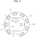
- Fig. 4 is a schematic plan view illustrating an example of the mounting substrate 72.
- Fig. 5 is a schematic sectional side view illustrating an example of the mounting substrate 72.
- the mounting substrate 72 is a multilayer substrate formed by building up a plurality of substrates 720 (four substrates 720 in the present embodiment).
- the mounting substrate 72 includes a first surface 721 which is a mounting surface on which the light emitting element 71 is mounted and a second surface 722 located on an opposite side of the first surface 721, and a heat radiator 9 is provided in close contact with the second surface 722. Accordingly, the heat radiator 9 and the mounting substrate 72 are thermally connected to each other.
- the first surface 721 which is a mounting surface on which the light emitting element 71 is mounted corresponds to a surface of the substrate 720 positioned on the most distal end side (the side of the objective lens 25), and the second surface 722 with which the heat radiator 9 is in close contact corresponds to a rear surface of the substrate 720 positioned on the most rear end side (the side of the bending section 21).
- a side surface located at a peripheral edge of the first surface 721 includes an inner peripheral side surface 723 that is an inner peripheral surface of the hole 73 formed in the annular mounting substrate 72 and an outer peripheral side surface 726 of the mounting substrate 72.
- the cutout portions 724 are formed on the side surface of the substrates 720 constituting the mounting substrate 72 as the multilayer substrate, and the cutout portions 724 of the substrates 720 are provided so as to be continuous in the thickness direction of the substrates 720, whereby groove-shaped cutout portions 724 along the thickness direction of the multilayer substrate are formed on the inner peripheral side surface 723 of the multilayer substrate.
- the cutout portions 724 may be formed in all the substrates 720 constituting the mounting substrate 72 (multilayer substrate) or may be formed only in part of the substrates 720 including at least the substrate 720 having the first surface 721 which is the mounting surface on which the light emitting element is 71 mounted.
- the cutout portion 724 is formed in the substrate 720 other than the substrate 720 with which the heat radiator 9 is in close contact among the plurality of substrates 720 constituting the multilayer substrate. In other words, the substrate 720 with which the heat radiator 9 is in close contact, that is, the substrate 720 of the second surface 722 is not provided with the cutout portion 724.
- the heat radiator 9 can be insulated from the conductive portion 725 provided in the cutout portion 724 of the other substrate 720 by the substrate 720 in close contact with the heat radiator 9.
- the conductive portion 725 is provided in the cutout portion 724 formed in the inner peripheral side surface 723, that is, a groove formed in the inner peripheral side surface 723 in the thickness direction.
- the conductive portion 725 is made of a conductive material having good conductivity such as copper, a copper alloy or a conductor paste, and is, for example, a cable connection land.
- the conductive portion 725 is provided so as to fill the cutout portion 724 (groove) formed in the inner peripheral side surface 723.
- An end portion of the conductive portion 725 on the first surface 721 side may be provided so as to be positioned on the first surface 721 and may have an L shape.
- a portion of the conductive portion 725 provided in the cutout portion 724 may correspond to a vertical side portion of the L shape
- a portion of the conductive portion 725 located on the first surface 721 may correspond to a horizontal side portion of the L shape.
- a core wire 81 of the power supply line 8 is joined to the portion of the conductive portion 725 corresponding to the vertical side portion of the L shape.
- the conductive portion 725 is electrically connected to a terminal of the light emitting element 71 or the light emitting element land 711 via a wiring pattern, a land, a through hole, or the like, provided on the first surface 721 and the surface of each layered substrate 720.
- the light emitting element 71 is constituted with an LED, or the like
- the conductive portion 725 includes the conductive portion 725 (positive electrode side conductive portion) connected to an anode (positive electrode side) of the LED and the conductive portion 725 (negative electrode side conductive portion) connected to a cathode (negative electrode side).
- the number of the conductive portions 725 is determined on the basis of an individual control mode for each of the plurality of light emitting elements 71. For example, in a case where brightness of each of the light emitting elements 71 (LED) is controlled when eight light emitting elements 71 (LED) are mounted, eight conductive portions 725 (positive electrode side conductive portions) may be provided on the anode side, and on the cathode side, one conductive portion 725 (negative electrode side conductive portion) obtained by combining the conductive portions into one circuit may be provided, or two conductive portions 725 (negative electrode side conductive portions) provided with redundancy against disconnection may be provided as two circuits. As described above, the number of cathode-side conductive portions 725 (negative electrode side conductive portions) may be smaller than the number of anode-side conductive portions 725 (positive electrode side conductive portions).
- the cutout portion 724 and the conductive portion 725 provided in the inner peripheral side surface 723 of the mounting substrate 72 may be formed by cutting a via hole (VIA) into half when forming (boring) the hole 73 so as to annularly form the mounting substrate 72 or may be pattern-formed after molding the mounting substrate 72.
- VIP via hole
- the core wire 81 of the power supply line 8 extending from the processor device 10 is joined to the conductive portion 725. Power from the processor device 10 is supplied to the light emitting module 7 via the power supply line 8 and the conductive portion 725 and turns on the light emitting element 71.
- the power supply line 8 extending from the processor device 10 side is connected so as to be parallel (parallel) to the conductive portion 725, that is, parallel to the groove-shaped cutout portion 724 along the thickness direction of the multilayer substrate with reference to an extending direction of the insertion tube 2.
- an axial direction of the core wire 81 of the power supply line 8 joined to the conductive portion 725 is parallel to the extending direction of the insertion tube 2 and becomes the thickness direction of the mounting substrate 72, and the core wire 81 is also located inside the hole 73 of the mounting substrate 72.
- the power supply line 8 extending from the processor device 10 side in this manner is connected in parallel to the conductive portion 725 in the extending direction of the insertion tube 2, so that it is possible to prevent bending of the power supply line 8 at a portion of the power supply line 8 in the vicinity of a portion to which the conductive portion 725 is connected. This makes it possible to prevent generation of stress acting in a direction in which the power supply line 8 is peeled off from the conductive portion 725 and to secure or improve connection strength between the power supply line 8 and the conductive portion 725.
- the heat radiator 9 is made of a metal having high thermal conductivity and is formed of an annular plate member similar to the mounting substrate 72. Similarly to the mounting substrate 72, the annular heat radiator 9 is provided with a hole at the center, and the hole of the heat radiator 9 and the hole 73 of the mounting substrate 72 form concentric circles.
- the plurality of power supply lines 8 and signal lines to be connected to the image sensor 6 are located inside the hole of the heat radiator 9.
- the heat radiator 9 is in close contact with the second surface 722 of the mounting substrate 72, and the mounting substrate 72 and the heat radiator 9 are thermally connected to each other. As a result, heat generated by the light emitting element 71 is dissipated to a surrounding space via the heat radiator 9, which prevents temperature rise of the light emitting element 71 and cools the light emitting element 71. It goes without saying that the second surface 722 of the mounting substrate 72 is electrically insulated from the heat radiator 9.
- the present invention is not limited to a case where the mounting substrate 72 (second surface 722) and the heat radiator 9 (adhesive surface 91) are in direct close contact with each other, and a heat conductive paste having insulating properties may be provided between the mounting substrate 72 (second surface 722) and the heat radiator 9 (close contact surface 91).
- the outer peripheral surface of the image sensor 6 faces the inner peripheral side surface 723 of the mounting substrate 72 on which the conductive portion 725 is provided, and a resin member, or the like, having insulating properties may be provided in a gap formed between the outer peripheral surface of the image sensor 6 and the inner peripheral side surface 723 of the mounting substrate 72.
- a resin member, or the like, having insulating properties may be provided in a gap formed between the outer peripheral surface of the image sensor 6 and the inner peripheral side surface 723 of the mounting substrate 72.
- the cutout portion 724 and the conductive portion 725 are provided on the inner peripheral side surface 723 of the mounting substrate 72, but are not limited thereto, and may be provided on the outer peripheral side surface 726 of the mounting substrate 72.
- the mounting substrate 72 is a multilayer substrate, but the present invention is not limited thereto, and the mounting substrate 72 may be a single-layer substrate including one substrate 720.
- the conductive portion 725 to which the power supply line 8 for supplying power to the light emitting element 71 is connected is provided on the inner peripheral side surface 723 located on the peripheral edge of the first surface 721 on which the light emitting element 71 is surface-mounted.
- the conductive portion 725 can be suitably arranged in the mounting substrate 72 that is to be included in the distal end portion of the insertion tube 2.
- An area of the first surface 721 can be reduced, and a size of the distal end portion of the insertion tube 2 into which the light emitting module 7 is to be incorporated can be reduced.
- a diameter of the hole 73 provided in the mounting substrate 72 can be increased, whereby a size of the image sensor 6 to be inserted and arranged in the hole 73 can be increased without increasing an outer diameter of the mounting substrate 72 and a size of the distal end portion of the insertion tube 2. It is possible to expand a mounting space of the first surface 721, improve a degree of freedom (degree of freedom in mounting) in arrangement of the light emitting elements 71 on the first surface 721 and increase the number of the light emitting elements 71 mounted, so that a large number of the plurality of light emitting elements 71 can be arranged.
- the conductive portion 725 is provided on the inner peripheral side surface 723 constituting the inner peripheral surface of the hole 73 through which the image sensor 6 is to be inserted, and thus, the conductive portion 725 can be provided inside the hole 73. This makes it possible to reduce the size of the distal end portion of the insertion tube 2.
- the conductive portion 725 is provided in the cutout portion 724 formed in the side surface, so that it is possible to reduce a height of a protrusion formed between the conductive portion 725 and the side surface on which the cutout portion 724 is not formed.
- the side surface on which the cutout portion 724 is formed is the inner peripheral side surface 723 constituting the inner peripheral surface of the hole 73
- by providing the conductive portion 725 in the cutout portion 724 it is possible to prevent the conductive portion 725 from protruding on the inner peripheral surface of the hole 73 and to increase the diameter of the hole 73.
- the mounting substrate 72 is constituted with the multilayer substrate in which the plurality of substrates 720 are built up, so that it is possible to improve a degree of freedom in wiring of a wiring pattern that connects the conductive portion 725 and the light emitting element 71.
- the heat radiator 9 such as a heat sink is in close contact with the second surface 722 located on the opposite side of the first surface 721 which is the mounting surface of the light emitting element 71.
- the substrate 720 other than the substrate 720 with which the heat radiator 9 is in close contact is provided with the cutout portion 724, but the substrate 720 with which the heat radiator 9 is in close contact, that is, the substrate 720 having the second surface 722 is not provided with the cutout portion 724.
- the conductive portion 725 is not provided on the substrate 720 (the substrate 720 including the second surface 722) with which the heat radiator 9 is in close contact.
- the heat radiator 9 can be insulated from the conductive portion 725 provided in the cutout portion 724 of the other substrate 720 by the substrate 720 in close contact with the heat radiator 9.
- the power supply line 8 extending from the processor device 10 side is connected in parallel to the conductive portion 725 in the extending direction of the insertion tube 2, so that it is possible to prevent the power supply line 8 from being bent at a portion of the power supply line 8 in the vicinity of the portion to which the conductive portion 725 is to be connected.
- This makes it possible to prevent generation of stress that peels off the power supply line 8 from conductive portion 725 and to improve connection strength (reliability of a soldered surface) between the power supply line 8 and the conductive portion 725.
- the power supply line 8 is prevented from being bent by providing the core wire 81 of the power supply line 8 on the inner peripheral side surface 723, so that interference with the image sensor 6 to be inserted into the central part of the hole 73 by a curved portion (R portion) due to the bending (bending) is eliminated.
- an inter-surface distance (clearance) between the inner peripheral side surface 723 of the mounting substrate 72 and the outer peripheral surface of the image sensor 6 only needs to be equal to an outer diameter dimension of the power supply line 8, so that it is possible to reduce an inner diameter dimension of the hole 73 of the mounting substrate 72 (inner diameter dimension of the mounting substrate 72).
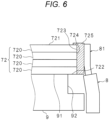
- Fig. 6 is a schematic sectional side view illustrating an example of the mounting substrate 72 according to a second embodiment (a recess 92 in the heat radiator 9).
- the cutout portions 724 are formed on the side surfaces of all the substrates 720 constituting the mounting substrate 72 which is a multilayer substrate, and the cutout portions 724 of the substrates 720 are provided so as to be continuous in the thickness direction of the substrate 720.
- a groove-shaped cutout portion 724 extending in the thickness direction is formed on the inner peripheral side surface 723 of the multilayer substrate.
- the substrate 720 with which the heat radiator 9 is in close contact that is, the substrate 720 having the second surface 722 is also provided with the cutout portion 724.
- the cutout portions 724 By forming the cutout portions 724 in all the substrates 720 constituting the mounting substrate 72 which is a multilayer substrate, the cutout portions 724 (groove) having the same length as a thickness of the mounting substrate 72 can be formed on the side surface of the mounting substrate 72, so that it is possible to increase a length of the cutout portion 724 parallel to the extending direction of the insertion tube 2.
- the conductive portion 725 is provided in the entire region of the cutout portion 724, so that it is possible to increase a length of the conductive portion 725 parallel to the extending direction of the insertion tube 2, increase a joint area for joining the conductive portion 725 and the core wire 81 of the power supply line 8 and improve joint strength between the conductive portion 725 and the core wire 81 (power supply line 8).
- the close contact surface 91 of the heat radiator 9 that is in close contact with the second surface of the mounting substrate 72 while facing the second surface 722 is provided with the recess 92 formed by missing (cutting out) part of an edge portion.
- the recess 92 is formed in the close contact surface 91 along an edge portion (inner peripheral edge) of the inner periphery of the hole of the annular heat radiator 9.
- the recesses 92 are provided corresponding to the conductive portions 725, and the number of the recesses 92 formed on the close contact surface 91 may be the same as the number of the conductive portions 725 provided on the inner peripheral side surface 723 of the mounting substrate 72.
- a positional correspondence relationship between the recess 92 and the conductive portion 725 includes a relationship in which a region of the recess 92 overlaps a region of the conductive portion 725 in a plan view of the mounting substrate 72, that is, in a direction perpendicular to the first surface 721 of the mounting substrate 72.
- the recess 92 provided in the close contact surface 91 can reliably separate the conductive portion 725 of the mounting substrate 72, in particular, a portion of the conductive portion 725 provided on the substrate 720 (the substrate 720 located on the most rear end side) having the second surface 722 from the heat radiator 9, so that an insulation distance can be secured between the conductive portion 725 and the heat radiator 9.
- the plurality of recesses 92 for securing the insulation distance between the conductive portion 725 and the heat radiator 9 are formed on the inner peripheral edge of the close contact surface 91 corresponding to the individual conductive portions 725, the present invention is not limited thereto.
- the recess 92 may be formed by missing (cutting out) the entire circumference at the inner peripheral edge of the hole provided in the close contact surface 91 of the heat radiator 9.
- the heat radiator 9 such as a heat sink is in close contact with the second surface 722 located on the opposite side of the first surface 721 which is the mounting surface of the light emitting element 71, and the recess 92 is provided on the close contact surface 91 of the heat radiator 9 in close contact with the second surface 722, that is, the surface (close contact surface 91) of the heat radiator 9 facing the second surface 722.
- the recess 92 provided in the close contact surface 91 can separate the conductive portion 725 of the mounting substrate 72 from the heat radiator 9, so that insulation of the heat radiator 9 from the conductive portion 725 can be ensured.
Landscapes
- Health & Medical Sciences (AREA)
- Life Sciences & Earth Sciences (AREA)
- Surgery (AREA)
- Physics & Mathematics (AREA)
- Optics & Photonics (AREA)
- Engineering & Computer Science (AREA)
- Medical Informatics (AREA)
- Animal Behavior & Ethology (AREA)
- Pathology (AREA)
- Radiology & Medical Imaging (AREA)
- Biophysics (AREA)
- Biomedical Technology (AREA)
- Heart & Thoracic Surgery (AREA)
- Veterinary Medicine (AREA)
- Molecular Biology (AREA)
- Nuclear Medicine, Radiotherapy & Molecular Imaging (AREA)
- General Health & Medical Sciences (AREA)
- Public Health (AREA)
- Microelectronics & Electronic Packaging (AREA)
- Astronomy & Astrophysics (AREA)
- General Physics & Mathematics (AREA)
- Endoscopes (AREA)
- Instruments For Viewing The Inside Of Hollow Bodies (AREA)
Abstract
Description
- The present disclosure relates to an endoscope.
- The present application claims priority based on
Japanese Patent Application No. 2021-017376 filed on February 5, 2021 - An endoscope is a medical instrument to be inserted into a body cavity of a subject to observe and treat a desired site and includes an imaging unit provided in a distal end portion of an insertion tube to be inserted into the body cavity, and an illumination device illuminating an imaging field of view of the imaging unit.
Patent Literature 1 discloses an endoscope including an illumination device for achieving illumination in a wide angular range of equal to or greater than 180 degrees to enable observation at a wide viewing angle. - Patent Literature 1:
JP 2015-16021 A - However, in the endoscope device described in
Patent Literature 1, there is a problem that, in providing a conductive portion to which a power supply line for supplying power to the illumination device is connected, suitable arrangement of the conductive portion is not considered. - In one aspect, an object is to provide an endoscope in which a conductive portion to which a power supply line for supplying power to a light emitting element is connected can be suitably arranged.
- An endoscope according to one aspect of the present disclosure is an endoscope including a light emitting module incorporated in a distal end portion of an insertion tube, in which the light emitting module includes a mounting substrate on which a plurality of light emitting elements is mounted, the mounting substrate has an annular shape in which a hole through which an image sensor using the light emitting elements as a light source is to be inserted is provided in a central portion and includes a first surface on which the light emitting elements are surface-mounted and a side surface located at a peripheral edge of the first surface, a conductive portion electrically connected to the light emitting elements is provided on the side surface, and a power supply line for supplying power to the light emitting elements is connected to the conductive portion.
- According to the present disclosure, it is possible to provide an endoscope in which a conductive portion to which a power supply line for supplying power to a light emitting element is connected is suitably arranged.
-
-
Fig. 1 is an external view of an endoscope according to a first embodiment. -
Fig. 2 is an enlarged view of a distal end portion of an insertion tube. -
Fig. 3 is an explanatory diagram for explaining an example of a connection state between a mounting substrate and a power supply line. -
Fig. 4 is a schematic plan view for explaining an example of the mounting substrate. -
Fig. 5 is a schematic sectional side view illustrating an example of the mounting substrate. -
Fig. 6 is a schematic sectional side view illustrating an example of a mounting substrate according to a second embodiment (a recess in a heat radiator). - Hereinafter, the present invention will be described in detail with reference to the drawings illustrating embodiments of the present invention.
Fig. 1 is an external view of anendoscope 1 according to a first embodiment. Theendoscope 1 includes aninsertion tube 2, an operation unit 3, auniversal tube 4, and aconnector unit 5. Theinsertion tube 2 is a portion to be inserted into a body cavity and includes a longsoft portion 20 and adistal end portion 22 connected to one end of thesoft portion 20 via abending section 21. The other end of thesoft portion 20 is connected to the operation unit 3 via acylindrical connection portion 23. Theuniversal tube 4 has one end connected to the operation unit 3 and extends in a direction different from theinsertion tube 2, and theconnector unit 5 is connected to the other end of theuniversal tube 4. - The operation unit 3 is provided to be gripped by a user (operator) of the
endoscope 1 such as a doctor to perform various kinds of operation and includes abending operation knob 30 and a plurality ofoperation buttons 31, and the like. Thebending operation knob 30 is connected to thebending section 21 by a wire (not illustrated) passing through inside of each of theconnection portion 23 and thesoft portion 20. Thebending section 21 is bent in two directions orthogonal to each other in an axial cross section through operation of thebending operation knob 30, thereby changing a direction of thedistal end portion 22 inserted into a body cavity. - The
endoscope 1 is connected to aprocessor device 10 via theconnector unit 5 and is used as anendoscope 1 device. Theprocessor device 10 includes a control unit, a storage unit, a signal processing circuit, and the like, and integrally controls the endoscope device by a control program stored in the storage unit. -
Fig. 2 is an enlarged view of the distal end portion of the insertion tube. Thedistal end portion 22 includes acylindrical housing 24 having one side fixed to thebending section 21. The other side of thehousing 24 is covered with a centralobjective lens 25 and an annularlight distribution lens 26 surrounding a periphery of theobjective lens 25. An image sensor 6 is provided inside thehousing 24 to face an inner side of theobjective lens 25. The image sensor 6 captures an image of a subject to be observed (an object), which is a body part such as a body cavity, through theobjective lens 25. Theobjective lens 25 is fitted into an inner frame of a hole provided in thedistal end portion 22 of theinsertion tube 2 and functions as an observation window. Alight emitting module 7 is incorporated so as face inside of thelight distribution lens 26. - The image sensor 6 includes a semiconductor element such as a complementary metal oxide semiconductor (CMOS) and an optical system for forming an image on an imaging surface of the image sensor and captures an image of inside of the body cavity through the
objective lens 25. Theobjective lens 25 is, for example, a wide-angle lens, and the image sensor 6 is constituted to capture an image at a viewing angle of equal to or greater than 180 degrees by setting the optical system including theobjective lens 25. The image sensor 6 outputs captured image data (image signal) of the subject to be observed (object) via a signal line joined to the image sensor 6. The captured image data (image signal) output from the image sensor 6 is subjected to preprocessing such as AD conversion or white balance correction, for example, and is output to theprocessor device 10. - The
light emitting module 7 includes anannular mounting substrate 72 surrounding a periphery of the image sensor 6 and a plurality oflight emitting elements 71 mounted on a first surface (mounting surface) of themounting substrate 72 facing thelight distribution lens 26. The plurality of light emitting elements includes, for example, a white LED, a narrowband LED, or a combination of both LEDs. The plurality of light emitting elements is arranged at equal intervals along a circumference of theannular mounting substrate 72, for example, one by one or two by two. A circular hole is formed in a central portion of theannular mounting substrate 72, and the image sensor 6 is located at the center of the circular hole. As a result, an outer peripheral surface of the image sensor 6 faces an inner peripheral surface (inner peripheral side surface) of the hole formed in themounting substrate 72. - The
light distribution lens 26 is a cylindrical lens having a shape extending outward from a peripheral edge portion of theobjective lens 25 and continuing to a peripheral wall of thehousing 24 through a bending portion. Light emitted from thelight emitting element 71 is emitted through thelight distribution lens 26 to illuminate an imaging field of view of the image sensor 6. The image sensor 6 captures an image under illumination by light emission of thelight emitting element 71. -
Fig. 3 is an explanatory diagram for explaining an example of a connection state between themounting substrate 72 and thepower supply line 8.Fig. 4 is a schematic plan view illustrating an example of themounting substrate 72.Fig. 5 is a schematic sectional side view illustrating an example of themounting substrate 72. Themounting substrate 72 is a multilayer substrate formed by building up a plurality of substrates 720 (foursubstrates 720 in the present embodiment). Themounting substrate 72 includes afirst surface 721 which is a mounting surface on which thelight emitting element 71 is mounted and asecond surface 722 located on an opposite side of thefirst surface 721, and aheat radiator 9 is provided in close contact with thesecond surface 722. Accordingly, theheat radiator 9 and themounting substrate 72 are thermally connected to each other. - In each
substrate 720 constituting themounting substrate 72 which is a multilayer substrate, thefirst surface 721 which is a mounting surface on which thelight emitting element 71 is mounted corresponds to a surface of thesubstrate 720 positioned on the most distal end side (the side of the objective lens 25), and thesecond surface 722 with which theheat radiator 9 is in close contact corresponds to a rear surface of thesubstrate 720 positioned on the most rear end side (the side of the bending section 21). - A side surface located at a peripheral edge of the
first surface 721 includes an innerperipheral side surface 723 that is an inner peripheral surface of thehole 73 formed in theannular mounting substrate 72 and an outerperipheral side surface 726 of themounting substrate 72. On the innerperipheral side surface 723, a plurality ofcutout portions 724 cut out in a thickness direction of themounting substrate 72 are formed. In other words, thecutout portions 724 are formed on the side surface of thesubstrates 720 constituting themounting substrate 72 as the multilayer substrate, and thecutout portions 724 of thesubstrates 720 are provided so as to be continuous in the thickness direction of thesubstrates 720, whereby groove-shaped cutout portions 724 along the thickness direction of the multilayer substrate are formed on the innerperipheral side surface 723 of the multilayer substrate. - The
cutout portions 724 may be formed in all thesubstrates 720 constituting the mounting substrate 72 (multilayer substrate) or may be formed only in part of thesubstrates 720 including at least thesubstrate 720 having thefirst surface 721 which is the mounting surface on which the light emitting element is 71 mounted. In the present embodiment, thecutout portion 724 is formed in thesubstrate 720 other than thesubstrate 720 with which theheat radiator 9 is in close contact among the plurality ofsubstrates 720 constituting the multilayer substrate. In other words, thesubstrate 720 with which theheat radiator 9 is in close contact, that is, thesubstrate 720 of thesecond surface 722 is not provided with thecutout portion 724. By not providing thecutout portion 724 and theconductive portion 725 in thesubstrate 720 in close contact with theheat radiator 9 among the plurality ofsubstrates 720 constituting the multilayer substrate as described above, theheat radiator 9 can be insulated from theconductive portion 725 provided in thecutout portion 724 of theother substrate 720 by thesubstrate 720 in close contact with theheat radiator 9. - The
conductive portion 725 is provided in thecutout portion 724 formed in the innerperipheral side surface 723, that is, a groove formed in the innerperipheral side surface 723 in the thickness direction. Theconductive portion 725 is made of a conductive material having good conductivity such as copper, a copper alloy or a conductor paste, and is, for example, a cable connection land. Theconductive portion 725 is provided so as to fill the cutout portion 724 (groove) formed in the innerperipheral side surface 723. - An end portion of the
conductive portion 725 on thefirst surface 721 side may be provided so as to be positioned on thefirst surface 721 and may have an L shape. As illustrated in the present embodiment, in the L-shapedconductive portion 725, a portion of theconductive portion 725 provided in thecutout portion 724 may correspond to a vertical side portion of the L shape, and a portion of theconductive portion 725 located on thefirst surface 721 may correspond to a horizontal side portion of the L shape. Acore wire 81 of thepower supply line 8 is joined to the portion of theconductive portion 725 corresponding to the vertical side portion of the L shape. - The
conductive portion 725 is electrically connected to a terminal of thelight emitting element 71 or the light emittingelement land 711 via a wiring pattern, a land, a through hole, or the like, provided on thefirst surface 721 and the surface of eachlayered substrate 720. As described above, thelight emitting element 71 is constituted with an LED, or the like, and theconductive portion 725 includes the conductive portion 725 (positive electrode side conductive portion) connected to an anode (positive electrode side) of the LED and the conductive portion 725 (negative electrode side conductive portion) connected to a cathode (negative electrode side). - The number of the
conductive portions 725 is determined on the basis of an individual control mode for each of the plurality oflight emitting elements 71. For example, in a case where brightness of each of the light emitting elements 71 (LED) is controlled when eight light emitting elements 71 (LED) are mounted, eight conductive portions 725 (positive electrode side conductive portions) may be provided on the anode side, and on the cathode side, one conductive portion 725 (negative electrode side conductive portion) obtained by combining the conductive portions into one circuit may be provided, or two conductive portions 725 (negative electrode side conductive portions) provided with redundancy against disconnection may be provided as two circuits. As described above, the number of cathode-side conductive portions 725 (negative electrode side conductive portions) may be smaller than the number of anode-side conductive portions 725 (positive electrode side conductive portions). - The
cutout portion 724 and theconductive portion 725 provided in the innerperipheral side surface 723 of the mountingsubstrate 72 may be formed by cutting a via hole (VIA) into half when forming (boring) thehole 73 so as to annularly form the mountingsubstrate 72 or may be pattern-formed after molding the mountingsubstrate 72. - The
core wire 81 of thepower supply line 8 extending from theprocessor device 10 is joined to theconductive portion 725. Power from theprocessor device 10 is supplied to thelight emitting module 7 via thepower supply line 8 and theconductive portion 725 and turns on thelight emitting element 71. - The
power supply line 8 extending from theprocessor device 10 side is connected so as to be parallel (parallel) to theconductive portion 725, that is, parallel to the groove-shapedcutout portion 724 along the thickness direction of the multilayer substrate with reference to an extending direction of theinsertion tube 2. As a result, an axial direction of thecore wire 81 of thepower supply line 8 joined to theconductive portion 725 is parallel to the extending direction of theinsertion tube 2 and becomes the thickness direction of the mountingsubstrate 72, and thecore wire 81 is also located inside thehole 73 of the mountingsubstrate 72. Thepower supply line 8 extending from theprocessor device 10 side in this manner is connected in parallel to theconductive portion 725 in the extending direction of theinsertion tube 2, so that it is possible to prevent bending of thepower supply line 8 at a portion of thepower supply line 8 in the vicinity of a portion to which theconductive portion 725 is connected. This makes it possible to prevent generation of stress acting in a direction in which thepower supply line 8 is peeled off from theconductive portion 725 and to secure or improve connection strength between thepower supply line 8 and theconductive portion 725. - The
heat radiator 9 is made of a metal having high thermal conductivity and is formed of an annular plate member similar to the mountingsubstrate 72. Similarly to the mountingsubstrate 72, theannular heat radiator 9 is provided with a hole at the center, and the hole of theheat radiator 9 and thehole 73 of the mountingsubstrate 72 form concentric circles. The plurality ofpower supply lines 8 and signal lines to be connected to the image sensor 6 are located inside the hole of theheat radiator 9. - The
heat radiator 9 is in close contact with thesecond surface 722 of the mountingsubstrate 72, and the mountingsubstrate 72 and theheat radiator 9 are thermally connected to each other. As a result, heat generated by thelight emitting element 71 is dissipated to a surrounding space via theheat radiator 9, which prevents temperature rise of thelight emitting element 71 and cools thelight emitting element 71. It goes without saying that thesecond surface 722 of the mountingsubstrate 72 is electrically insulated from theheat radiator 9. The present invention is not limited to a case where the mounting substrate 72 (second surface 722) and the heat radiator 9 (adhesive surface 91) are in direct close contact with each other, and a heat conductive paste having insulating properties may be provided between the mounting substrate 72 (second surface 722) and the heat radiator 9 (close contact surface 91). - The outer peripheral surface of the image sensor 6 faces the inner
peripheral side surface 723 of the mountingsubstrate 72 on which theconductive portion 725 is provided, and a resin member, or the like, having insulating properties may be provided in a gap formed between the outer peripheral surface of the image sensor 6 and the innerperipheral side surface 723 of the mountingsubstrate 72. By providing the insulating resin member, or the like, sealed in the gap, it is possible to secure insulation between the image sensor 6 and theconductive portion 725 and thecore wire 81 connected to theconductive portion 725. - In the present embodiment, the
cutout portion 724 and theconductive portion 725 are provided on the innerperipheral side surface 723 of the mountingsubstrate 72, but are not limited thereto, and may be provided on the outerperipheral side surface 726 of the mountingsubstrate 72. In the present embodiment, the mountingsubstrate 72 is a multilayer substrate, but the present invention is not limited thereto, and the mountingsubstrate 72 may be a single-layer substrate including onesubstrate 720. - According to the present embodiment, the
conductive portion 725 to which thepower supply line 8 for supplying power to thelight emitting element 71 is connected is provided on the innerperipheral side surface 723 located on the peripheral edge of thefirst surface 721 on which thelight emitting element 71 is surface-mounted. As a result, it is not necessary to provide the conductive portion 725 (a portion of theconductive portion 725 to be joined to the core wire 81) on thefirst surface 721, and theconductive portion 725 can be suitably arranged in the mountingsubstrate 72 that is to be included in the distal end portion of theinsertion tube 2. An area of thefirst surface 721 can be reduced, and a size of the distal end portion of theinsertion tube 2 into which thelight emitting module 7 is to be incorporated can be reduced. By reducing the area of thefirst surface 721, a diameter of thehole 73 provided in the mountingsubstrate 72 can be increased, whereby a size of the image sensor 6 to be inserted and arranged in thehole 73 can be increased without increasing an outer diameter of the mountingsubstrate 72 and a size of the distal end portion of theinsertion tube 2. It is possible to expand a mounting space of thefirst surface 721, improve a degree of freedom (degree of freedom in mounting) in arrangement of thelight emitting elements 71 on thefirst surface 721 and increase the number of thelight emitting elements 71 mounted, so that a large number of the plurality oflight emitting elements 71 can be arranged. Theconductive portion 725 is provided on the innerperipheral side surface 723 constituting the inner peripheral surface of thehole 73 through which the image sensor 6 is to be inserted, and thus, theconductive portion 725 can be provided inside thehole 73. This makes it possible to reduce the size of the distal end portion of theinsertion tube 2. - According to the present embodiment, the
conductive portion 725 is provided in thecutout portion 724 formed in the side surface, so that it is possible to reduce a height of a protrusion formed between theconductive portion 725 and the side surface on which thecutout portion 724 is not formed. In a case where the side surface on which thecutout portion 724 is formed is the innerperipheral side surface 723 constituting the inner peripheral surface of thehole 73, by providing theconductive portion 725 in thecutout portion 724, it is possible to prevent theconductive portion 725 from protruding on the inner peripheral surface of thehole 73 and to increase the diameter of thehole 73. - According to the present embodiment, the mounting
substrate 72 is constituted with the multilayer substrate in which the plurality ofsubstrates 720 are built up, so that it is possible to improve a degree of freedom in wiring of a wiring pattern that connects theconductive portion 725 and thelight emitting element 71. In the mountingsubstrate 72 constituted with a multilayer substrate, theheat radiator 9 such as a heat sink is in close contact with thesecond surface 722 located on the opposite side of thefirst surface 721 which is the mounting surface of thelight emitting element 71. Among the plurality ofsubstrates 720 constituting the multilayer substrate, thesubstrate 720 other than thesubstrate 720 with which theheat radiator 9 is in close contact is provided with thecutout portion 724, but thesubstrate 720 with which theheat radiator 9 is in close contact, that is, thesubstrate 720 having thesecond surface 722 is not provided with thecutout portion 724. Thus, theconductive portion 725 is not provided on the substrate 720 (thesubstrate 720 including the second surface 722) with which theheat radiator 9 is in close contact. By not providing thecutout portion 724 and theconductive portion 725 in thesubstrate 720 in close contact with theheat radiator 9 among the plurality ofsubstrates 720 constituting the multilayer substrate as described above, theheat radiator 9 can be insulated from theconductive portion 725 provided in thecutout portion 724 of theother substrate 720 by thesubstrate 720 in close contact with theheat radiator 9. - According to the present embodiment, the
power supply line 8 extending from theprocessor device 10 side is connected in parallel to theconductive portion 725 in the extending direction of theinsertion tube 2, so that it is possible to prevent thepower supply line 8 from being bent at a portion of thepower supply line 8 in the vicinity of the portion to which theconductive portion 725 is to be connected. This makes it possible to prevent generation of stress that peels off thepower supply line 8 fromconductive portion 725 and to improve connection strength (reliability of a soldered surface) between thepower supply line 8 and theconductive portion 725. Thepower supply line 8 is prevented from being bent by providing thecore wire 81 of thepower supply line 8 on the innerperipheral side surface 723, so that interference with the image sensor 6 to be inserted into the central part of thehole 73 by a curved portion (R portion) due to the bending (bending) is eliminated. As a result, an inter-surface distance (clearance) between the innerperipheral side surface 723 of the mountingsubstrate 72 and the outer peripheral surface of the image sensor 6 only needs to be equal to an outer diameter dimension of thepower supply line 8, so that it is possible to reduce an inner diameter dimension of thehole 73 of the mounting substrate 72 (inner diameter dimension of the mounting substrate 72). -
Fig. 6 is a schematic sectional side view illustrating an example of the mountingsubstrate 72 according to a second embodiment (arecess 92 in the heat radiator 9). In the present embodiment, thecutout portions 724 are formed on the side surfaces of all thesubstrates 720 constituting the mountingsubstrate 72 which is a multilayer substrate, and thecutout portions 724 of thesubstrates 720 are provided so as to be continuous in the thickness direction of thesubstrate 720. As a result, a groove-shapedcutout portion 724 extending in the thickness direction is formed on the innerperipheral side surface 723 of the multilayer substrate. In other words, thesubstrate 720 with which theheat radiator 9 is in close contact, that is, thesubstrate 720 having thesecond surface 722 is also provided with thecutout portion 724. - By forming the
cutout portions 724 in all thesubstrates 720 constituting the mountingsubstrate 72 which is a multilayer substrate, the cutout portions 724 (groove) having the same length as a thickness of the mountingsubstrate 72 can be formed on the side surface of the mountingsubstrate 72, so that it is possible to increase a length of thecutout portion 724 parallel to the extending direction of theinsertion tube 2. Theconductive portion 725 is provided in the entire region of thecutout portion 724, so that it is possible to increase a length of theconductive portion 725 parallel to the extending direction of theinsertion tube 2, increase a joint area for joining theconductive portion 725 and thecore wire 81 of thepower supply line 8 and improve joint strength between theconductive portion 725 and the core wire 81 (power supply line 8). - The
close contact surface 91 of theheat radiator 9 that is in close contact with the second surface of the mountingsubstrate 72 while facing thesecond surface 722 is provided with therecess 92 formed by missing (cutting out) part of an edge portion. Therecess 92 is formed in theclose contact surface 91 along an edge portion (inner peripheral edge) of the inner periphery of the hole of theannular heat radiator 9. - The
recesses 92 are provided corresponding to theconductive portions 725, and the number of therecesses 92 formed on theclose contact surface 91 may be the same as the number of theconductive portions 725 provided on the innerperipheral side surface 723 of the mountingsubstrate 72. A positional correspondence relationship between therecess 92 and theconductive portion 725 includes a relationship in which a region of therecess 92 overlaps a region of theconductive portion 725 in a plan view of the mountingsubstrate 72, that is, in a direction perpendicular to thefirst surface 721 of the mountingsubstrate 72. - The
recess 92 provided in theclose contact surface 91 can reliably separate theconductive portion 725 of the mountingsubstrate 72, in particular, a portion of theconductive portion 725 provided on the substrate 720 (thesubstrate 720 located on the most rear end side) having thesecond surface 722 from theheat radiator 9, so that an insulation distance can be secured between theconductive portion 725 and theheat radiator 9. - Although the plurality of
recesses 92 for securing the insulation distance between theconductive portion 725 and theheat radiator 9 are formed on the inner peripheral edge of theclose contact surface 91 corresponding to the individualconductive portions 725, the present invention is not limited thereto. Therecess 92 may be formed by missing (cutting out) the entire circumference at the inner peripheral edge of the hole provided in theclose contact surface 91 of theheat radiator 9. - According to the present embodiment, in the mounting
substrate 72, theheat radiator 9 such as a heat sink is in close contact with thesecond surface 722 located on the opposite side of thefirst surface 721 which is the mounting surface of thelight emitting element 71, and therecess 92 is provided on theclose contact surface 91 of theheat radiator 9 in close contact with thesecond surface 722, that is, the surface (close contact surface 91) of theheat radiator 9 facing thesecond surface 722. Therecess 92 provided in theclose contact surface 91 can separate theconductive portion 725 of the mountingsubstrate 72 from theheat radiator 9, so that insulation of theheat radiator 9 from theconductive portion 725 can be ensured. - It should be noted that the embodiments disclosed herein are illustrative in all respects and are not restrictive. The technical features described in the embodiments can be combined with each other, and the scope of the present invention is intended to include all modifications and equivalents within the scope of the claims.
-
- 1
- endoscope
- 10
- processor device
- 2
- insertion tube
- 20
- soft portion
- 21
- bending section
- 22
- distal end portion
- 23
- connection portion
- 24
- housing
- 25
- objective lens
- 26
- light distribution lens
- 3
- operation unit
- 30
- bending operation knob
- 31
- operation button
- 4
- universal tube
- 5
- connector unit
- 6
- image sensor
- 7
- light emitting module
- 71
- light emitting element
- 711
- light emitting element land
- 72
- mounting substrate
- 720
- substrate
- 721
- first surface
- 722
- second surface
- 723
- inner peripheral side surface
- 724
- cutout portion
- 725
- conductive portion (positive electrode side conductive portion, negative electrode side conductive portion)
- 726
- outer peripheral side surface
- 73
- hole
- 8
- power supply line
- 81
- core wire
- 9
- heat radiator
- 91
- close contact surface
- 92
- recess
Claims (7)
- An endoscope comprising a light emitting module incorporated in a distal end portion of an insertion tube,the light emitting module including a mounting substrate on which a plurality of light emitting elements is mounted,the mounting substrate having an annular shape in which a hole through which an image sensor using the light emitting elements as a light source is to be inserted is provided in a central portion and including a first surface on which the light emitting elements are surface-mounted and a side surface located at a peripheral edge of the first surface,a conductive portion electrically connected to the light emitting elements being provided on the side surface, anda power supply line for supplying power to the light emitting elements being connected to the conductive portion.
- The endoscope according to claim 1,
wherein the side surface is an inner peripheral side surface constituting an inner peripheral surface of the hole. - The endoscope according to claim 1 or 2,wherein a cutout portion is formed in the side surface, andthe conductive portion is provided in the cutout portion.
- The endoscope according to claim 3,wherein the mounting substrate is a multilayer substrate in which a plurality of substrates is built up,a heat radiator is in close contact with a second surface located on an opposite side of the first surface, andthe cutout portion is formed in a substrate other than a substrate with which the heat radiator is in close contact among the plurality of substrates constituting the multilayer substrate.
- The endoscope according to any one of claims 1 to 3,wherein a heat radiator is in close contact with a second surface located on an opposite side of the first surface,a recess is provided on a close contact surface of the heat radiator, the close contact surface being in close contact with the second surface, andthe heat radiator is separated from the conductive portion by the recess.
- The endoscope according to any one of claims 1 to 5,wherein the power supply line extends from a processor device side to be connected to the endoscope, andis connected in parallel to the conductive portion in an extending direction of the insertion tube.
- The endoscope according to any one of claims 1 to 6,wherein the conductive portion includes positive electrode side conductive portions to be connected to a positive electrode side of the light emitting elements and negative electrode side conductive portions to be connected to a negative electrode side of the light emitting elements, anda number of the negative electrode side conductive portions to be connected to the negative electrode side is smaller than a number of the positive electrode side conductive portions to be connected to the positive electrode side.
Applications Claiming Priority (2)
| Application Number | Priority Date | Filing Date | Title |
|---|---|---|---|
| JP2021017376A JP7512219B2 (en) | 2021-02-05 | 2021-02-05 | Endoscope |
| PCT/JP2022/000340 WO2022168528A1 (en) | 2021-02-05 | 2022-01-07 | Endoscope |
Publications (2)
| Publication Number | Publication Date |
|---|---|
| EP4223209A1 true EP4223209A1 (en) | 2023-08-09 |
| EP4223209A4 EP4223209A4 (en) | 2024-10-02 |
Family
ID=82742324
Family Applications (1)
| Application Number | Title | Priority Date | Filing Date |
|---|---|---|---|
| EP22749407.7A Pending EP4223209A4 (en) | 2021-02-05 | 2022-01-07 | ENDOSCOPE |
Country Status (5)
| Country | Link |
|---|---|
| US (1) | US12514440B2 (en) |
| EP (1) | EP4223209A4 (en) |
| JP (2) | JP7512219B2 (en) |
| CN (1) | CN116490813B (en) |
| WO (1) | WO2022168528A1 (en) |
Family Cites Families (25)
| Publication number | Priority date | Publication date | Assignee | Title |
|---|---|---|---|---|
| JPH11267099A (en) * | 1998-03-24 | 1999-10-05 | Olympus Optical Co Ltd | Endoscope |
| JP4598164B2 (en) | 2000-08-14 | 2010-12-15 | Hoya株式会社 | Endoscope |
| JP4388288B2 (en) * | 2003-02-19 | 2009-12-24 | オリンパス株式会社 | Endoscope |
| US8435173B2 (en) * | 2003-10-06 | 2013-05-07 | Olympus Corporation | Endoscope |
| JP4488286B2 (en) | 2003-11-12 | 2010-06-23 | オリンパス株式会社 | Capsule medical device |
| JP4460923B2 (en) * | 2004-03-09 | 2010-05-12 | オリンパス株式会社 | Endoscope device |
| JP4632677B2 (en) * | 2004-03-11 | 2011-02-16 | オリンパス株式会社 | Endoscope device |
| JP4519494B2 (en) * | 2004-03-25 | 2010-08-04 | オリンパス株式会社 | Endoscope device |
| US7762950B2 (en) * | 2004-03-25 | 2010-07-27 | Olympus Corporation | Endoscope |
| JP4917436B2 (en) * | 2004-10-25 | 2012-04-18 | オリンパス株式会社 | Endoscope device |
| JP4987257B2 (en) * | 2005-06-29 | 2012-07-25 | オリンパス株式会社 | Endoscope |
| US20070049794A1 (en) | 2005-09-01 | 2007-03-01 | Ezc Medical Llc | Visualization stylet for medical device applications having self-contained power source |
| JP5139599B2 (en) * | 2010-10-25 | 2013-02-06 | オリンパスメディカルシステムズ株式会社 | Endoscope |
| JP2012230235A (en) * | 2011-04-26 | 2012-11-22 | Olympus Corp | Endoscope |
| JP3175343U (en) * | 2012-02-17 | 2012-05-10 | 宋文恭 | Lamp heat sink structure |
| JP2014000314A (en) * | 2012-06-20 | 2014-01-09 | Hoya Corp | Heat radiation structure of endoscope distal end |
| JP6192398B2 (en) | 2013-07-09 | 2017-09-06 | オリンパス株式会社 | Lighting device |
| TWI583024B (en) | 2014-05-30 | 2017-05-11 | 榮晶生物科技股份有限公司 | Light-emitting diode package structure and camera module including the same |
| US9532706B2 (en) * | 2014-08-07 | 2017-01-03 | Welch Allyn, Inc. | Vaginal speculum with illuminator |
| CN208657154U (en) * | 2015-03-20 | 2019-03-26 | 3M创新有限公司 | Flexible multilayer substrate for attaching light emitting semiconductor devices |
| JP2018138111A (en) | 2017-02-24 | 2018-09-06 | オリンパス株式会社 | Led type tip optical adaptor |
| WO2019044802A1 (en) * | 2017-08-28 | 2019-03-07 | Hoya株式会社 | Endoscope light source device and endoscope system |
| US10743755B1 (en) | 2018-10-11 | 2020-08-18 | InnovaQuartz LLC | Multi-spectrum ring illuminated surgical camera |
| JP7257278B2 (en) | 2019-07-18 | 2023-04-13 | デンカ株式会社 | EXPANSION COMPOSITION FOR CEMENT AND CEMENT COMPOSITION |
| EP4084667A1 (en) * | 2019-12-30 | 2022-11-09 | Boston Scientific Scimed, Inc. | Devices for locating a body lumen |
-
2021
- 2021-02-05 JP JP2021017376A patent/JP7512219B2/en active Active
-
2022
- 2022-01-07 CN CN202280007269.5A patent/CN116490813B/en active Active
- 2022-01-07 WO PCT/JP2022/000340 patent/WO2022168528A1/en not_active Ceased
- 2022-01-07 US US18/033,868 patent/US12514440B2/en active Active
- 2022-01-07 EP EP22749407.7A patent/EP4223209A4/en active Pending
-
2024
- 2024-06-26 JP JP2024103207A patent/JP7668934B2/en active Active
Also Published As
| Publication number | Publication date |
|---|---|
| WO2022168528A1 (en) | 2022-08-11 |
| CN116490813B (en) | 2025-11-04 |
| US20240008729A1 (en) | 2024-01-11 |
| JP2024114855A (en) | 2024-08-23 |
| JP2022120467A (en) | 2022-08-18 |
| JP7668934B2 (en) | 2025-04-25 |
| CN116490813A (en) | 2023-07-25 |
| EP4223209A4 (en) | 2024-10-02 |
| US12514440B2 (en) | 2026-01-06 |
| JP7512219B2 (en) | 2024-07-08 |
Similar Documents
| Publication | Publication Date | Title |
|---|---|---|
| US11957305B2 (en) | Endoscope distal end structure and endoscope | |
| US9325881B2 (en) | Imaging mechanism and endoscope apparatus | |
| EP1604606A1 (en) | Capsule type endoscope | |
| US10574866B2 (en) | Imaging unit and endoscope apparatus | |
| EP2913850A1 (en) | Imaging device, endoscope, semiconductor device, and method of manufacturing semiconductor device | |
| US9927113B2 (en) | Heat sink structure and LED heat sink assemblies | |
| EP3050491B1 (en) | Endoscope device | |
| EP2197333A1 (en) | Image pickup device and endoscope provided with image pickup device | |
| US20230007769A1 (en) | Electronic module, method of manufacturing electronic module, and endoscope | |
| CN113164021B (en) | Endoscope front end structure and endoscope | |
| US12514440B2 (en) | Endoscope | |
| US10456013B2 (en) | Cable connection structure, imaging apparatus, and endoscope | |
| JP6099541B2 (en) | Endoscope and endoscope manufacturing method | |
| JP7702341B2 (en) | Endoscope imaging device and endoscope | |
| JP5466913B2 (en) | Endoscope device | |
| WO2017115441A1 (en) | Mounting structure, image pickup device, and endoscope | |
| JP2007014488A (en) | Endoscope | |
| JP5361596B2 (en) | Adapter and endoscope | |
| JP2015008901A (en) | Imaging unit and endoscope apparatus | |
| JP2021164525A (en) | Endoscope | |
| JP4519494B2 (en) | Endoscope device | |
| JP2024139204A (en) | Mounting board and endoscope | |
| JP5586212B2 (en) | Endoscope device | |
| JP2012230235A (en) | Endoscope | |
| JP2000089132A (en) | Endoscope tip for side view |
Legal Events
| Date | Code | Title | Description |
|---|---|---|---|
| STAA | Information on the status of an ep patent application or granted ep patent |
Free format text: STATUS: THE INTERNATIONAL PUBLICATION HAS BEEN MADE |
|
| PUAI | Public reference made under article 153(3) epc to a published international application that has entered the european phase |
Free format text: ORIGINAL CODE: 0009012 |
|
| STAA | Information on the status of an ep patent application or granted ep patent |
Free format text: STATUS: REQUEST FOR EXAMINATION WAS MADE |
|
| 17P | Request for examination filed |
Effective date: 20230503 |
|
| AK | Designated contracting states |
Kind code of ref document: A1 Designated state(s): AL AT BE BG CH CY CZ DE DK EE ES FI FR GB GR HR HU IE IS IT LI LT LU LV MC MK MT NL NO PL PT RO RS SE SI SK SM TR |
|
| DAV | Request for validation of the european patent (deleted) | ||
| DAX | Request for extension of the european patent (deleted) | ||
| REG | Reference to a national code |
Ref country code: DE Ref legal event code: R079 Free format text: PREVIOUS MAIN CLASS: A61B0001060000 Ipc: A61B0001000000 |
|
| A4 | Supplementary search report drawn up and despatched |
Effective date: 20240902 |
|
| RIC1 | Information provided on ipc code assigned before grant |
Ipc: A61B 1/12 20060101ALI20240827BHEP Ipc: G02B 23/26 20060101ALI20240827BHEP Ipc: A61B 1/06 20060101ALI20240827BHEP Ipc: A61B 1/00 20060101AFI20240827BHEP |