EP4220942A1 - Rc oscillation circuit - Google Patents
Rc oscillation circuit Download PDFInfo
- Publication number
- EP4220942A1 EP4220942A1 EP22879605.8A EP22879605A EP4220942A1 EP 4220942 A1 EP4220942 A1 EP 4220942A1 EP 22879605 A EP22879605 A EP 22879605A EP 4220942 A1 EP4220942 A1 EP 4220942A1
- Authority
- EP
- European Patent Office
- Prior art keywords
- inverters
- signal
- group
- input
- latch
- Prior art date
- Legal status (The legal status is an assumption and is not a legal conclusion. Google has not performed a legal analysis and makes no representation as to the accuracy of the status listed.)
- Granted
Links
Images


Classifications
-
- H—ELECTRICITY
- H03—ELECTRONIC CIRCUITRY
- H03B—GENERATION OF OSCILLATIONS, DIRECTLY OR BY FREQUENCY-CHANGING, BY CIRCUITS EMPLOYING ACTIVE ELEMENTS WHICH OPERATE IN A NON-SWITCHING MANNER; GENERATION OF NOISE BY SUCH CIRCUITS
- H03B5/00—Generation of oscillations using amplifier with regenerative feedback from output to input
- H03B5/20—Generation of oscillations using amplifier with regenerative feedback from output to input with frequency-determining element comprising resistance and either capacitance or inductance, e.g. phase-shift oscillator
-
- H—ELECTRICITY
- H03—ELECTRONIC CIRCUITRY
- H03B—GENERATION OF OSCILLATIONS, DIRECTLY OR BY FREQUENCY-CHANGING, BY CIRCUITS EMPLOYING ACTIVE ELEMENTS WHICH OPERATE IN A NON-SWITCHING MANNER; GENERATION OF NOISE BY SUCH CIRCUITS
- H03B5/00—Generation of oscillations using amplifier with regenerative feedback from output to input
- H03B5/02—Details
- H03B5/04—Modifications of generator to compensate for variations in physical values, e.g. power supply, load, temperature
-
- H—ELECTRICITY
- H03—ELECTRONIC CIRCUITRY
- H03B—GENERATION OF OSCILLATIONS, DIRECTLY OR BY FREQUENCY-CHANGING, BY CIRCUITS EMPLOYING ACTIVE ELEMENTS WHICH OPERATE IN A NON-SWITCHING MANNER; GENERATION OF NOISE BY SUCH CIRCUITS
- H03B5/00—Generation of oscillations using amplifier with regenerative feedback from output to input
- H03B5/02—Details
- H03B5/06—Modifications of generator to ensure starting of oscillations
-
- H—ELECTRICITY
- H03—ELECTRONIC CIRCUITRY
- H03B—GENERATION OF OSCILLATIONS, DIRECTLY OR BY FREQUENCY-CHANGING, BY CIRCUITS EMPLOYING ACTIVE ELEMENTS WHICH OPERATE IN A NON-SWITCHING MANNER; GENERATION OF NOISE BY SUCH CIRCUITS
- H03B5/00—Generation of oscillations using amplifier with regenerative feedback from output to input
- H03B5/08—Generation of oscillations using amplifier with regenerative feedback from output to input with frequency-determining element comprising lumped inductance and capacitance
-
- H—ELECTRICITY
- H03—ELECTRONIC CIRCUITRY
- H03K—PULSE TECHNIQUE
- H03K19/00—Logic circuits, i.e. having at least two inputs acting on one output; Inverting circuits
- H03K19/20—Logic circuits, i.e. having at least two inputs acting on one output; Inverting circuits characterised by logic function, e.g. AND, OR, NOR, NOT circuits
-
- H—ELECTRICITY
- H03—ELECTRONIC CIRCUITRY
- H03K—PULSE TECHNIQUE
- H03K3/00—Circuits for generating electric pulses; Monostable, bistable or multistable circuits
- H03K3/02—Generators characterised by the type of circuit or by the means used for producing pulses
- H03K3/027—Generators characterised by the type of circuit or by the means used for producing pulses by the use of logic circuits, with internal or external positive feedback
- H03K3/037—Bistable circuits
-
- H—ELECTRICITY
- H03—ELECTRONIC CIRCUITRY
- H03K—PULSE TECHNIQUE
- H03K3/00—Circuits for generating electric pulses; Monostable, bistable or multistable circuits
- H03K3/02—Generators characterised by the type of circuit or by the means used for producing pulses
- H03K3/027—Generators characterised by the type of circuit or by the means used for producing pulses by the use of logic circuits, with internal or external positive feedback
- H03K3/037—Bistable circuits
- H03K3/0375—Bistable circuits provided with means for increasing reliability; for protection; for ensuring a predetermined initial state when the supply voltage has been applied; for storing the actual state when the supply voltage fails
-
- H—ELECTRICITY
- H03—ELECTRONIC CIRCUITRY
- H03K—PULSE TECHNIQUE
- H03K5/00—Manipulating of pulses not covered by one of the other main groups of this subclass
- H03K5/13—Arrangements having a single output and transforming input signals into pulses delivered at desired time intervals
- H03K5/135—Arrangements having a single output and transforming input signals into pulses delivered at desired time intervals by the use of time reference signals, e.g. clock signals
-
- H—ELECTRICITY
- H03—ELECTRONIC CIRCUITRY
- H03K—PULSE TECHNIQUE
- H03K5/00—Manipulating of pulses not covered by one of the other main groups of this subclass
- H03K5/156—Arrangements in which a continuous pulse train is transformed into a train having a desired pattern
- H03K5/1565—Arrangements in which a continuous pulse train is transformed into a train having a desired pattern the output pulses having a constant duty cycle
Definitions
- the present disclosure relates to a technical field of electronics, and in particular to a resistor-capacitor oscillation circuit.
- RC resistor-capacitor
- a charging switch of the capacitors is turned off through feedback control, and a discharging switch of the capacitors is further turned on through the feedback control.
- the feed control is generally performed through a hysteresis comparator.
- the feedback control is performed through two hysteresis comparators.
- current RC oscillators basically need the hysteresis comparators to determine the level of the voltage of the capacitors and to perform the feedback control on the charging switch and the discharging switch.
- the way of determining the level of the voltage of the capacitors by the comparators has a problem about a dead state of outputting. For example, if an output node of the comparator comes to an intermediate level due to external force, a whole loop circuit may stop oscillating and enter a steady state; and even though the external force is removed, the loop circuit can still not automatically recover for oscillation. Therefore, it is necessary to provide a recovery circuit with respect to the dead state of outputting for different circuits, which increases circuit areas and power consumption cost, and further increases level of design difficulty.
- the present disclosure aims to overcome at least one of the above technical problems and provides a resistor-capacitor (RC) oscillation circuit.
- RC resistor-capacitor
- the present disclosure provides the RC oscillation circuit, including a first group of inverters, a second group of inverters, a latch, a delay circuit, and a third group of inverters.
- the first group of the inverters is connected to the delay circuit, and is configured to generate a first signal A and a second signal B, and input the first signal A and the second signal B into the delay circuit.
- a potential of the first signal A is opposite to a potential of the second signal B.
- An input end of the second group of the inverters is connected to an enable signal EN.
- An output end of the second group of the inverters is connected to the latch.
- the second group of the inverters is configured to generate an inverted signal ENB opposite to the enable signal EN and input the inverted signal ENB into the latch.
- An output end of the delay circuit is connected to the latch, and is configured to delay the first signal A and the second signal B and output a first delay signal DA and a second delay signal DB to the latch.
- the latch is connected to the third group of the inverters.
- the latch includes a first output end and a second output end.
- the latch receives the first delay signal DA and the second delay signal DB.
- the latch generates a first clock signal FB and a second clock signal FA and receives the first clock signal FB and the second clock signal FA.
- the first output end is connected to the third group of the inverters and inputs the first clock signal FB to the third group of the inverters.
- the first output end is further connected to an input end of the first group of the inverters.
- the first clock signal FB serves as an input of the first group of the inverters.
- an output signal CLK is output by an output end of the third group of the inverters.
- the first group of the inverters includes two inverters connected in series.
- the first group of the inverters respectively output the first signal A and the second signal B through output ends of the two inverters.
- the delay circuit includes a first delay circuit and a second delay circuit.
- the first delay circuit and the second delay circuit are respectively connected to the output ends of the two inverters.
- the latch includes a three-input NOR gate and a two-input NOR gate.
- An output end of the first delay circuit is connected to a DA input end of the three-input NOR gate.
- the output end of the second group of the inverters is connected to an ENB input end of the three-input NOR gate.
- An output end of the two-input NOR gate is connected to an FA input end of the three-input NOR gate.
- An FB input end of the two-input NOR gate is connected to an output end of the three-input NOR gate.
- a DB input end of the two-input NOR gate is connected to an output end of the second delay circuit.
- the second group of the inverters includes an odd number of inverters.
- a quantity of inverters of the third group of the inverters is determined according to loads to be connected.
- a quantity of inverters of the third group of the inverters is determined according to phase of the output signal CLK.
- the present disclosure further provides a resistor-capacitor (RC) oscillation circuit, including: a first group of inverters, a latch, a delay circuit, and a third group of inverters.
- RC resistor-capacitor
- the first group of the inverters is connected to the delay circuit, and is configured to generate a first signal A and a second signal B, and input the first signal A and the second signal B into the delay circuit.
- a potential of the first signal A is opposite to a potential of the second signal B.
- An output end of the delay circuit is connected to the latch, and is configured to delay the first signal A and the second signal B and output a first delay signal DA and a second delay signal DB to the latch.
- An input end of the latch is further connected to an enable signal EN port.
- An output end of the latch is connected to the third group of the inverters.
- the latch includes a first output end and a second output end.
- the latch receives the first delay signal DA and the second delay signal DB.
- the latch generates a first clock signal FB and a second clock signal FA and receives the first clock signal FB and the second clock signal FA.
- the first output end is connected to the third group of the inverters and inputs the first clock signal FB to the third group of the inverters.
- the first output end is further connected to an input end of the first group of the inverters.
- the first clock signal FB serves as an input of the first group of the inverters.
- an output signal CLK is output by an output end of the third group of the inverters.
- the first group of the inverters includes two inverters connected in series.
- the first group of the inverters respectively output the first signal A and the second signal B through output ends of the two inverters.
- the delay circuit includes a first delay circuit and a second delay circuit. The first delay circuit and the second delay circuit are respectively connected to the output ends of the two inverters.
- the latch includes a three-input NOR gate and a two-input NOR gate.
- An output end of the first delay circuit is connected to a DA input end of the three-input NOR gate.
- the output end of the second group of the inverters is connected to an EN input end of the three-input NOR gate.
- An output end of the two-input NOR gate is connected to an FA input end of the three-input NOR gate.
- An FB input end of the two-input NOR gate is connected to an output end of the three-input NOR gate.
- a DB input end of the two-input NOR gate is connected to an output end of the second delay circuit.
- any node in an RC oscillator is pulled to an abnormal level by an abnormal external force.
- the RC oscillator is forced to be at a high level or forced to be at a low level, and after the external force is removed, the RC oscillation circuit may automatically recover for oscillation without additionally providing any recovery circuit for a dead state of outputting.
- the embodiment of the present disclosure provides a resistor-capacitor (RC) oscillation circuit, including a first group of inverters 10, a second group of inverters 20, a latch 40, a delay circuit 30, and a third group of inverters 50.
- RC resistor-capacitor
- the first group of the inverters 10 is connected to the delay circuit 30, and is configured to generate a first signal A and a second signal B, and input the first signal A and the second signal B into the delay circuit 30.
- a potential of the first signal A is opposite to a potential of the second signal B.
- An input end of the second group of the inverters 20 is connected to an enable signal EN.
- An output end of the second group of the inverters 20 is connected to the latch 40.
- the second group of the inverters 20 is configured to generate an inverted signal ENB opposite to the enable signal EN and input the inverted signal ENB into the latch 40 to control the circuit enable, which is effective for high level.
- An output end of the delay circuit 30 is connected to the latch 40, and is configured to delay the first signal A and the second signal B and output a first delay signal DA and a second delay signal DB to the latch 40.
- the latch 40 is connected to the third group of the inverters 50.
- the latch 40 includes a first output end and a second output end.
- the latch 40 receives the first delay signal DA and the second delay signal DB.
- the latch 40 generates a first clock signal FB and a second clock signal FA and receives the first clock signal FB and the second clock signal FA.
- the first output end is connected to the third group of the inverters 50 and inputs the first clock signal FB to the third group of the inverters 50.
- the first output end is further connected to an input end of the first group of the inverters 10.
- the first clock signal FB serves as an input of the first group of the inverters 10, that is, the first clock signal FB is used as a feedback input of the RC oscillation circuit. After the first clock signal FB is driven by the third group of the inverters 50, an output signal CLK is output by an output end of the third group of the inverters 50.
- the first group of the inverters 10 includes two inverters connected in series.
- the first group of the inverters 10 respectively output the first signal A and the second signal B through output ends of the two inverters.
- a delay length of the delay circuit 30 is freely adjusted according to duty ratio required by an output clock.
- the delay circuit 30 includes a first delay circuit 31 and a second delay circuit 32.
- the first delay circuit 31 and the second delay circuit 32 are respectively connected to the output ends of the two inverters, receive the input first signal A and the input second signal B, and respectively perform delay processing on the first signal A and the second signal B.
- the first delay circuit 31 performs delay processing on the first signal A and then outputs the first delay signal DA.
- the second delay circuit 32 performs delay processing on the second signal B and then outputs the second delay signal DB.
- the latch 40 includes a three-input NOR gate and a two-input NOR gate.
- An output end of the first delay circuit 31 is connected to a DA input end of the three-input NOR gate, which is configured to input the first delay signal DA.
- the output end of the second group of the inverters is connected to an ENB input end of the three-input NOR gate, which is configured to input the inverted signal ENB.
- An output end of the two-input NOR gate is connected to an FA input end of the three-input NOR gate, and the second clock signal FA output by an input NOT gate is used as an input of the FA input end of the three-input NOR gate.
- An FB input end of the two-input NOR gate is connected to an output end of the three-input NOR gate, which is configured to receive the first clock signal FB output by the three-input NOR gate.
- a DB input end of the two-input NOR gate is connected to an output end of the second delay circuit, which is configured to receive the second delay signal output by the second delay circuit 32.
- the latch 40 outputs switching of the first clock signal FB according to a high level of the DA input end and a high level of the DB input end, and latches and holds the first clock signal FB before next high level arrives, and an enable signal EN of the first clock signal FB is effective at a low level.
- the first clock signal FB generates a falling edge that is controlled and generated by a rising edge of the first delay signal DA.
- the rising edge of the first clock signal FB is triggered by the falling edge generated after the second clock signal FA and the first delay signal DA.
- An order of the falling edge of the second clock signal FA and the falling edge of the first delay signal DA is determined by sizes of delay time tdA and delay time tdB of the delay circuit.
- the second clock signal FA generates a falling edge that is controlled and generated by a rising edge of the second delay signal DB.
- the rising edge of the second clock signal FA is triggered by the falling edge generated after the first clock signal FB and the second delay signal DB.
- An order of the falling edge of the first clock signal FB and the falling edge of the second delay signal DB is determined by the sizes of the delay time tdA and the delay time tdB of the delay circuit.
- the duty ratio of the output signal CLK is the delay time tdA of the first delay circuit.
- a period of the output signal CLK is sum of a delay time of the first delay circuit and a delay time of the second delay circuit, namely tdA + tdB.
- the second group of the inverters 20 includes an odd number of inverters, and specifically includes one inverter, which is configured to generate the inverted signal ENB opposite to the enable signal EN.
- a quantity of inverters of the third group of the inverters 50 is determined according to loads to be connected.
- a quantity of inverters of the third group of the inverters 50 is determined according to phase of the output signal CLK.
- any nodes of EN, ENB, A, B, DA, DB, FA, and FB in an RC oscillator is pulled to an abnormal level by an abnormal external force, for example, the RC oscillator is forced to be at a high level or forced to be at a low level, and after the external force is removed, the RC oscillation circuit may automatically recover for oscillation without additionally providing any recovery circuit for a dead state of outputting.
- the first clock signal FB is at a low level, at this time, the second signal B is at a high level, the first signal A is at a low level, and after the second signal B and the first signal A are delayed, the first clock signal FB should be turned to a high level.
- the first signal A is pulled to a high level through strong external force
- the first delay signal DA is pulled to a high level after passing through the delay circuit
- the first clock signal FB is kept at a low level
- the strong external force is removed, due to a fact that the first clock signal FB is at a low level
- the first signal A is pulled to the low level again, the circuit recovers to a normal working state, and the oscillation is restarted.
- Other nodes may further be analyzed by a same method.
- the embodiment of the present disclosure provides a resistor-capacitor (RC) oscillation circuit.
- RC resistor-capacitor
- an enable signal EN is effective at a low level, at this time, the enable signal is directly connected to an ENB port of a latch, and there is no need to provide the second group of the inverters.
Landscapes
- Physics & Mathematics (AREA)
- Nonlinear Science (AREA)
- Engineering & Computer Science (AREA)
- Computer Hardware Design (AREA)
- Computing Systems (AREA)
- General Engineering & Computer Science (AREA)
- Mathematical Physics (AREA)
- Manipulation Of Pulses (AREA)
- Pulse Circuits (AREA)
- Stabilization Of Oscillater, Synchronisation, Frequency Synthesizers (AREA)
Abstract
Description
- The present disclosure relates to a technical field of electronics, and in particular to a resistor-capacitor oscillation circuit.
- Currently, periodically charging and discharging capacitors through resistors is a basic principle of resistor-capacitor (RC) oscillators. When a voltage of the capacitors reaches a certain level, a charging switch of the capacitors is turned off through feedback control, and a discharging switch of the capacitors is further turned on through the feedback control. If there is only one capacitor to be charged and discharged, the feed control is generally performed through a hysteresis comparator. If there are two groups of the capacitors to be charged and discharged, the feedback control is performed through two hysteresis comparators. However, current RC oscillators basically need the hysteresis comparators to determine the level of the voltage of the capacitors and to perform the feedback control on the charging switch and the discharging switch.
- Moreover, the way of determining the level of the voltage of the capacitors by the comparators has a problem about a dead state of outputting. For example, if an output node of the comparator comes to an intermediate level due to external force, a whole loop circuit may stop oscillating and enter a steady state; and even though the external force is removed, the loop circuit can still not automatically recover for oscillation. Therefore, it is necessary to provide a recovery circuit with respect to the dead state of outputting for different circuits, which increases circuit areas and power consumption cost, and further increases level of design difficulty.
- The present disclosure aims to overcome at least one of the above technical problems and provides a resistor-capacitor (RC) oscillation circuit.
- In order to achieve the above purpose, on one hand, the present disclosure provides the RC oscillation circuit, including a first group of inverters, a second group of inverters, a latch, a delay circuit, and a third group of inverters.
- The first group of the inverters is connected to the delay circuit, and is configured to generate a first signal A and a second signal B, and input the first signal A and the second signal B into the delay circuit. A potential of the first signal A is opposite to a potential of the second signal B.
- An input end of the second group of the inverters is connected to an enable signal EN. An output end of the second group of the inverters is connected to the latch. The second group of the inverters is configured to generate an inverted signal ENB opposite to the enable signal EN and input the inverted signal ENB into the latch.
- An output end of the delay circuit is connected to the latch, and is configured to delay the first signal A and the second signal B and output a first delay signal DA and a second delay signal DB to the latch.
- The latch is connected to the third group of the inverters. The latch includes a first output end and a second output end. The latch receives the first delay signal DA and the second delay signal DB. The latch generates a first clock signal FB and a second clock signal FA and receives the first clock signal FB and the second clock signal FA. The first output end is connected to the third group of the inverters and inputs the first clock signal FB to the third group of the inverters. The first output end is further connected to an input end of the first group of the inverters. The first clock signal FB serves as an input of the first group of the inverters.
- After the first clock signal FB is driven by the third group of the inverters, an output signal CLK is output by an output end of the third group of the inverters.
- Furthermore, the first group of the inverters includes two inverters connected in series. The first group of the inverters respectively output the first signal A and the second signal B through output ends of the two inverters.
- Furthermore, the delay circuit includes a first delay circuit and a second delay circuit. The first delay circuit and the second delay circuit are respectively connected to the output ends of the two inverters.
- Furthermore, the latch includes a three-input NOR gate and a two-input NOR gate. An output end of the first delay circuit is connected to a DA input end of the three-input NOR gate. The output end of the second group of the inverters is connected to an ENB input end of the three-input NOR gate. An output end of the two-input NOR gate is connected to an FA input end of the three-input NOR gate.
- An FB input end of the two-input NOR gate is connected to an output end of the three-input NOR gate. A DB input end of the two-input NOR gate is connected to an output end of the second delay circuit.
- Furthermore, the second group of the inverters includes an odd number of inverters.
- Furthermore, a quantity of inverters of the third group of the inverters is determined according to loads to be connected.
- Furthermore, a quantity of inverters of the third group of the inverters is determined according to phase of the output signal CLK.
- On the other hand, the present disclosure further provides a resistor-capacitor (RC) oscillation circuit, including: a first group of inverters, a latch, a delay circuit, and a third group of inverters.
- The first group of the inverters is connected to the delay circuit, and is configured to generate a first signal A and a second signal B, and input the first signal A and the second signal B into the delay circuit. A potential of the first signal A is opposite to a potential of the second signal B.
- An output end of the delay circuit is connected to the latch, and is configured to delay the first signal A and the second signal B and output a first delay signal DA and a second delay signal DB to the latch.
- An input end of the latch is further connected to an enable signal EN port. An output end of the latch is connected to the third group of the inverters. The latch includes a first output end and a second output end. The latch receives the first delay signal DA and the second delay signal DB. The latch generates a first clock signal FB and a second clock signal FA and receives the first clock signal FB and the second clock signal FA. The first output end is connected to the third group of the inverters and inputs the first clock signal FB to the third group of the inverters. The first output end is further connected to an input end of the first group of the inverters. The first clock signal FB serves as an input of the first group of the inverters.
- After the first clock signal FB is driven by the third group of the inverters, an output signal CLK is output by an output end of the third group of the inverters.
- Furthermore, the first group of the inverters includes two inverters connected in series. The first group of the inverters respectively output the first signal A and the second signal B through output ends of the two inverters. The delay circuit includes a first delay circuit and a second delay circuit. The first delay circuit and the second delay circuit are respectively connected to the output ends of the two inverters.
- Furthermore, the latch includes a three-input NOR gate and a two-input NOR gate. An output end of the first delay circuit is connected to a DA input end of the three-input NOR gate. The output end of the second group of the inverters is connected to an EN input end of the three-input NOR gate. An output end of the two-input NOR gate is connected to an FA input end of the three-input NOR gate.
- An FB input end of the two-input NOR gate is connected to an output end of the three-input NOR gate. A DB input end of the two-input NOR gate is connected to an output end of the second delay circuit.
- Compared with prior art, in the embodiments of the present disclosure, any node in an RC oscillator is pulled to an abnormal level by an abnormal external force. For example, the RC oscillator is forced to be at a high level or forced to be at a low level, and after the external force is removed, the RC oscillation circuit may automatically recover for oscillation without additionally providing any recovery circuit for a dead state of outputting.
- In order to more clearly illustrate technical solutions in embodiments of the present disclosure, drawings that need to be used in description of the embodiments are briefly described below. In an obvious way, the drawings in the following description are merely some embodiments of the present disclosure, and for a person of ordinary skill in art, other drawings are obtained according to the drawings without involving any inventive effort, wherein:
-
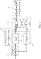
FIG. 1 is a schematic diagram of a resistor-capacitor (RC) oscillation circuit according to one embodiment of the present disclosure. -
FIG. 2 is a timing schematic diagram of the RC oscillation circuit according to one embodiment of the present disclosure. -
FIG. 3 is a schematic diagram of the RC oscillation circuit according to another embodiment of the present disclosure. - Technical solutions in embodiments of the present disclosure are clearly and completely described below in conjunction with drawings in the embodiments of the present disclosure, and obviously, the described embodiments are only a part of the embodiments of the present disclosure rather than all embodiments. Based on the embodiments of the present disclosure, all other embodiments obtained by a person of ordinary skill in art without creative efforts shall fall within a protection scope of the present disclosure.
- Referring to
FIG. 1 , the embodiment of the present disclosure provides a resistor-capacitor (RC) oscillation circuit, including a first group ofinverters 10, a second group ofinverters 20, alatch 40, adelay circuit 30, and a third group ofinverters 50. - The first group of the
inverters 10 is connected to thedelay circuit 30, and is configured to generate a first signal A and a second signal B, and input the first signal A and the second signal B into thedelay circuit 30. A potential of the first signal A is opposite to a potential of the second signal B. An input end of the second group of theinverters 20 is connected to an enable signal EN. An output end of the second group of theinverters 20 is connected to thelatch 40. The second group of theinverters 20 is configured to generate an inverted signal ENB opposite to the enable signal EN and input the inverted signal ENB into thelatch 40 to control the circuit enable, which is effective for high level. An output end of thedelay circuit 30 is connected to thelatch 40, and is configured to delay the first signal A and the second signal B and output a first delay signal DA and a second delay signal DB to thelatch 40. Thelatch 40 is connected to the third group of theinverters 50. Thelatch 40 includes a first output end and a second output end. Thelatch 40 receives the first delay signal DA and the second delay signal DB. Thelatch 40 generates a first clock signal FB and a second clock signal FA and receives the first clock signal FB and the second clock signal FA. The first output end is connected to the third group of theinverters 50 and inputs the first clock signal FB to the third group of theinverters 50. The first output end is further connected to an input end of the first group of theinverters 10. The first clock signal FB serves as an input of the first group of theinverters 10, that is, the first clock signal FB is used as a feedback input of the RC oscillation circuit. After the first clock signal FB is driven by the third group of theinverters 50, an output signal CLK is output by an output end of the third group of theinverters 50. - In the embodiment, the first group of the
inverters 10 includes two inverters connected in series. The first group of theinverters 10 respectively output the first signal A and the second signal B through output ends of the two inverters. - In the embodiment, a delay length of the
delay circuit 30 is freely adjusted according to duty ratio required by an output clock. Thedelay circuit 30 includes afirst delay circuit 31 and asecond delay circuit 32. Thefirst delay circuit 31 and thesecond delay circuit 32 are respectively connected to the output ends of the two inverters, receive the input first signal A and the input second signal B, and respectively perform delay processing on the first signal A and the second signal B. Thefirst delay circuit 31 performs delay processing on the first signal A and then outputs the first delay signal DA. Thesecond delay circuit 32 performs delay processing on the second signal B and then outputs the second delay signal DB. - In the embodiment, the
latch 40 includes a three-input NOR gate and a two-input NOR gate. An output end of thefirst delay circuit 31 is connected to a DA input end of the three-input NOR gate, which is configured to input the first delay signal DA. The output end of the second group of the inverters is connected to an ENB input end of the three-input NOR gate, which is configured to input the inverted signal ENB. An output end of the two-input NOR gate is connected to an FA input end of the three-input NOR gate, and the second clock signal FA output by an input NOT gate is used as an input of the FA input end of the three-input NOR gate. - An FB input end of the two-input NOR gate is connected to an output end of the three-input NOR gate, which is configured to receive the first clock signal FB output by the three-input NOR gate. A DB input end of the two-input NOR gate is connected to an output end of the second delay circuit, which is configured to receive the second delay signal output by the
second delay circuit 32. - The
latch 40 outputs switching of the first clock signal FB according to a high level of the DA input end and a high level of the DB input end, and latches and holds the first clock signal FB before next high level arrives, and an enable signal EN of the first clock signal FB is effective at a low level. - As shown in
FIG. 2 , the first clock signal FB generates a falling edge that is controlled and generated by a rising edge of the first delay signal DA. The rising edge of the first clock signal FB is triggered by the falling edge generated after the second clock signal FA and the first delay signal DA. An order of the falling edge of the second clock signal FA and the falling edge of the first delay signal DA is determined by sizes of delay time tdA and delay time tdB of the delay circuit. The second clock signal FA generates a falling edge that is controlled and generated by a rising edge of the second delay signal DB. The rising edge of the second clock signal FA is triggered by the falling edge generated after the first clock signal FB and the second delay signal DB. An order of the falling edge of the first clock signal FB and the falling edge of the second delay signal DB is determined by the sizes of the delay time tdA and the delay time tdB of the delay circuit. - In the embodiment, the duty ratio of the output signal CLK is the delay time tdA of the first delay circuit. A period of the output signal CLK is sum of a delay time of the first delay circuit and a delay time of the second delay circuit, namely tdA + tdB.
- In the embodiment, the second group of the
inverters 20 includes an odd number of inverters, and specifically includes one inverter, which is configured to generate the inverted signal ENB opposite to the enable signal EN. - In one embodiment, a quantity of inverters of the third group of the
inverters 50 is determined according to loads to be connected. - In another embodiment, a quantity of inverters of the third group of the
inverters 50 is determined according to phase of the output signal CLK. - Any nodes of EN, ENB, A, B, DA, DB, FA, and FB in an RC oscillator is pulled to an abnormal level by an abnormal external force, for example, the RC oscillator is forced to be at a high level or forced to be at a low level, and after the external force is removed, the RC oscillation circuit may automatically recover for oscillation without additionally providing any recovery circuit for a dead state of outputting. For example, it is assumed that the first clock signal FB is at a low level, at this time, the second signal B is at a high level, the first signal A is at a low level, and after the second signal B and the first signal A are delayed, the first clock signal FB should be turned to a high level. At this time, the first signal A is pulled to a high level through strong external force, the first delay signal DA is pulled to a high level after passing through the delay circuit, the first clock signal FB is kept at a low level, and the circuit stops oscillating. After the strong external force is removed, due to a fact that the first clock signal FB is at a low level, the first signal A is pulled to the low level again, the circuit recovers to a normal working state, and the oscillation is restarted. Other nodes may further be analyzed by a same method.
- Referring to
FIG. 3 , the embodiment of the present disclosure provides a resistor-capacitor (RC) oscillation circuit. Different from Embodiment 1, in the embodiment, an enable signal EN is effective at a low level, at this time, the enable signal is directly connected to an ENB port of a latch, and there is no need to provide the second group of the inverters. - The above is only embodiments of the present disclosure, and it should be noted that, for a person of ordinary skill in the art, improvement is made without departing from a concept of the present disclosure, but these are all within the protection scope of the present disclosure.
Claims (10)
- A resistor-capacitor (RC) oscillation circuit, comprising:a first group of inverters;a second group of inverters;a latch;a delay circuit; anda third group of inverters;wherein the first group of the inverters is connected to the delay circuit, and is configured to generate a first signal A and a second signal B, and input the first signal A and the second signal B into the delay circuit, a potential of the first signal A is opposite to a potential of the second signal B;an input end of the second group of the inverters is connected to an enable signal EN, an output end of the second group of the inverters is connected to the latch, and the second group of the inverters is configured to generate an inverted signal ENB opposite to the enable signal EN and input the inverted signal ENB into the latch;an output end of the delay circuit is connected to the latch, and is configured to delay the first signal A and the second signal B and output a first delay signal DA and a second delay signal DB to the latch;the latch is connected to the third group of the inverters, the latch comprises a first output end and a second output end, the latch receives the first delay signal DA and the second delay signal DB, the latch generates a first clock signal FB and a second clock signal FA and receives the first clock signal FB and the second clock signal FA; the first output end is connected to the third group of the inverters and inputs the first clock signal FB to the third group of the inverters; the first output end is further connected to an input end of the first group of the inverters, the first clock signal FB serves as an input of the first group of the inverters; andafter the first clock signal FB is driven by the third group of the inverters, an output signal CLK is output by an output end of the third group of the inverters.
- The RC oscillation circuit according to claim 1, wherein the first group of the inverters comprises two inverters connected in series, and the first group of the inverters respectively output the first signal A and the second signal B through output ends of the two inverters.
- The RC oscillation circuit according to claim 2, wherein the delay circuit comprises a first delay circuit and a second delay circuit, and the first delay circuit and the second delay circuit are respectively connected to the output ends of the two inverters.
- The RC oscillation circuit according to claim 3, wherein the latch comprises a three-input NOR gate and a two-input NOR gate, an output end of the first delay circuit is connected to a DA input end of the three-input NOR gate, the output end of the second group of the inverters is connected to an ENB input end of the three-input NOR gate, an output end of the two-input NOR gate is connected to an FA input end of the three-input NOR gate; and
an FB input end of the two-input NOR gate is connected to an output end of the three-input NOR gate, and a DB input end of the two-input NOR gate is connected to an output end of the second delay circuit. - The RC oscillation circuit according to claim 1, wherein the second group of the inverters comprises an odd number of inverters.
- The RC oscillation circuit according to claim 1, wherein a quantity of inverters of the third group of the inverters is determined according to loads to be connected.
- The RC oscillation circuit according to claim 1, wherein a quantity of inverters of the third group of the inverters is determined according to phase of the output signal CLK.
- A resistor-capacitor (RC) oscillation circuit, comprising:a first group of inverters;a latch;a delay circuit; anda third group of inverters;wherein the first group of the inverters is connected to the delay circuit, the first group of the inverters is configured to generate a first signal A and a second signal B and input the first signal A and the second signal B into the delay circuit, and a potential of the first signal A is opposite to a potential of the second signal B;an output end of the delay circuit is connected to the latch, and is configured to delay the first signal A and the second signal B and output a first delay signal DA and a second delay signal DB to the latch;an input end of the latch is further connected to an enable signal EN port, an output end the latch is connected to the third group of the inverters, the latch comprises a first output end and a second output end, the latch receives the first delay signal DA and the second delay signal DB, the latch generates a first clock signal FB and a second clock signal FA and receives the first clock signal FB and the second clock signal FA; the first output end is connected to the third group of the inverters and inputs the first clock signal FB to the third group of the inverters; the first output end is further connected to an input end of the first group of the inverters, the first clock signal FB serves as an input of the first group of the inverters; andafter the first clock signal FB is driven by the third group of the inverters, an output signal CLK is output by an output end of the third group of the inverters.
- The RC oscillation circuit according to claim 8, wherein the first group of the inverters comprises two inverters connected in series, the first group of the inverters respectively output the first signal A and the second signal B through output ends of the two inverters, the delay circuit comprises a first delay circuit and a second delay circuit, and the first delay circuit and the second delay circuit are respectively connected to the output ends of the two inverters.
- The RC oscillation circuit according to claim 9, wherein the latch comprises a three-input NOR gate and a two-input NOR gate, an output end of the first delay circuit is connected to a DA input end of the three-input NOR gate, the output end of the second group of the inverters is connected to an EN input end of the three-input NOR gate, an output end of the two-input NOR gate is connected to an FA input end of the three-input NOR gate; and
an FB input end of the two-input NOR gate is connected to an output end of the three-input NOR gate, and a DB input end of the two-input NOR gate is connected to an output end of the second delay circuit.
Applications Claiming Priority (2)
| Application Number | Priority Date | Filing Date | Title |
|---|---|---|---|
| CN202111302765.7A CN113746427B (en) | 2021-11-05 | 2021-11-05 | RC oscillating circuit |
| PCT/CN2022/078379 WO2023077694A1 (en) | 2021-11-05 | 2022-02-28 | Rc oscillation circuit |
Publications (3)
| Publication Number | Publication Date |
|---|---|
| EP4220942A1 true EP4220942A1 (en) | 2023-08-02 |
| EP4220942A4 EP4220942A4 (en) | 2024-08-07 |
| EP4220942B1 EP4220942B1 (en) | 2025-04-30 |
Family
ID=78727536
Family Applications (1)
| Application Number | Title | Priority Date | Filing Date |
|---|---|---|---|
| EP22879605.8A Active EP4220942B1 (en) | 2021-11-05 | 2022-02-28 | Rc oscillation circuit |
Country Status (7)
| Country | Link |
|---|---|
| US (1) | US11848644B2 (en) |
| EP (1) | EP4220942B1 (en) |
| JP (1) | JP7542748B2 (en) |
| KR (1) | KR102807933B1 (en) |
| CN (1) | CN113746427B (en) |
| ES (1) | ES3032216T3 (en) |
| WO (1) | WO2023077694A1 (en) |
Families Citing this family (3)
| Publication number | Priority date | Publication date | Assignee | Title |
|---|---|---|---|---|
| CN113746427B (en) * | 2021-11-05 | 2022-02-11 | 深圳飞骧科技股份有限公司 | RC oscillating circuit |
| CN115589217B (en) * | 2022-12-07 | 2023-03-24 | 深圳飞骧科技股份有限公司 | RC oscillating circuit |
| CN117792302A (en) * | 2023-12-29 | 2024-03-29 | 无锡芯亿集成电路有限公司 | Power amplifying device capable of compensating power |
Family Cites Families (25)
| Publication number | Priority date | Publication date | Assignee | Title |
|---|---|---|---|---|
| JPS56129422A (en) * | 1980-03-17 | 1981-10-09 | Nippon Telegr & Teleph Corp <Ntt> | Oscillation circuit |
| JPS60216625A (en) * | 1984-04-12 | 1985-10-30 | Fuji Electric Corp Res & Dev Ltd | oscillation circuit |
| JPS63299407A (en) * | 1987-05-28 | 1988-12-06 | Nec Corp | Oscillation circuit |
| US5532653A (en) * | 1995-02-07 | 1996-07-02 | National Semiconductor Corporation | Supply voltage compensated charge pump oscillator |
| JP2941692B2 (en) * | 1995-08-08 | 1999-08-25 | エル・ジー・セミコン・カンパニー・リミテッド | Timer oscillation circuit |
| JPH1013194A (en) * | 1996-06-19 | 1998-01-16 | Oki Electric Ind Co Ltd | Oscillation circuit and pll circuit |
| JP3019814B2 (en) * | 1997-09-18 | 2000-03-13 | 日本電気株式会社 | Clock recovery circuit |
| US5889441A (en) * | 1997-12-12 | 1999-03-30 | Scenix Semiconductor, Inc. | Temperature and voltage independent on-chip oscillator system and method |
| JP3742345B2 (en) * | 2002-01-10 | 2006-02-01 | 富士通株式会社 | OSCILLATOR CIRCUIT, SEMICONDUCTOR DEVICE HAVING THE OSCILLATOR CIRCUIT, AND SEMICONDUCTOR MEMORY DEVICE HAVING THE OSCILLATOR CIRCUIT |
| KR100626387B1 (en) * | 2004-09-22 | 2006-09-20 | 삼성전자주식회사 | Oscillation Circuit of Semiconductor Memory Device |
| US7102452B1 (en) * | 2004-12-31 | 2006-09-05 | Zilog, Inc. | Temperature-compensated RC oscillator |
| JP4159570B2 (en) * | 2005-09-07 | 2008-10-01 | 富士通株式会社 | OSCILLATOR CIRCUIT, SEMICONDUCTOR DEVICE HAVING THE OSCILLATOR CIRCUIT, AND SEMICONDUCTOR MEMORY DEVICE HAVING THE OSCILLATOR CIRCUIT |
| JP4989106B2 (en) * | 2006-05-17 | 2012-08-01 | オンセミコンダクター・トレーディング・リミテッド | Oscillator circuit |
| KR20080021393A (en) * | 2006-09-04 | 2008-03-07 | 주식회사 하이닉스반도체 | Oscillator of Semiconductor Device |
| US20100328199A1 (en) * | 2009-06-30 | 2010-12-30 | Silicon Laboratories Inc. | Lcd controller with bypass mode |
| CN103401553B (en) * | 2013-07-19 | 2016-02-03 | 电子科技大学 | A kind of synclator circuit |
| CN104537995A (en) * | 2014-12-30 | 2015-04-22 | 深圳市华星光电技术有限公司 | Gate drive circuit and shift register |
| CN206698185U (en) * | 2016-02-25 | 2017-12-01 | 宗仁科技(平潭)有限公司 | A kind of oscillating circuit and oscillator |
| CN109039307B (en) * | 2018-08-30 | 2022-07-05 | 华润微集成电路(无锡)有限公司 | Double-edge anti-shake circuit structure |
| US10734949B2 (en) * | 2018-11-13 | 2020-08-04 | Silicon Laboratories Inc. | Self enabling signal conditioner for conditioning a crystal oscillator output signal into a compliant clock signal |
| JP7404632B2 (en) * | 2019-03-28 | 2023-12-26 | セイコーエプソン株式会社 | Output circuits, circuit devices, oscillators, electronic equipment and mobile objects |
| US20210099128A1 (en) * | 2019-10-01 | 2021-04-01 | Macronix International Co., Ltd. | Relaxation oscillator circuit with process variation compensation |
| CN111800110A (en) * | 2020-03-16 | 2020-10-20 | 上海明矽微电子有限公司 | An RC oscillator circuit for RFID tag chip |
| CN113746427B (en) * | 2021-11-05 | 2022-02-11 | 深圳飞骧科技股份有限公司 | RC oscillating circuit |
| CN113852353B (en) * | 2021-11-25 | 2022-02-15 | 深圳飞骧科技股份有限公司 | RC oscillator and electronic equipment |
-
2021
- 2021-11-05 CN CN202111302765.7A patent/CN113746427B/en active Active
-
2022
- 2022-02-28 WO PCT/CN2022/078379 patent/WO2023077694A1/en not_active Ceased
- 2022-02-28 KR KR1020237022079A patent/KR102807933B1/en active Active
- 2022-02-28 JP JP2023535999A patent/JP7542748B2/en active Active
- 2022-02-28 ES ES22879605T patent/ES3032216T3/en active Active
- 2022-02-28 EP EP22879605.8A patent/EP4220942B1/en active Active
-
2023
- 2023-04-07 US US18/131,872 patent/US11848644B2/en active Active
Also Published As
| Publication number | Publication date |
|---|---|
| ES3032216T3 (en) | 2025-07-16 |
| EP4220942B1 (en) | 2025-04-30 |
| WO2023077694A1 (en) | 2023-05-11 |
| KR20230111247A (en) | 2023-07-25 |
| CN113746427A (en) | 2021-12-03 |
| CN113746427B (en) | 2022-02-11 |
| US11848644B2 (en) | 2023-12-19 |
| US20230253920A1 (en) | 2023-08-10 |
| EP4220942A4 (en) | 2024-08-07 |
| JP7542748B2 (en) | 2024-08-30 |
| KR102807933B1 (en) | 2025-05-15 |
| JP2023552890A (en) | 2023-12-19 |
Similar Documents
| Publication | Publication Date | Title |
|---|---|---|
| US11848644B2 (en) | Resistor-capacitor oscillation circuit | |
| US8060771B2 (en) | Glitch-free clock suspend and resume circuit | |
| US7570104B2 (en) | Charge pump circuit control system | |
| CN112929009B (en) | RC relaxation oscillator | |
| CN107294506B (en) | Crystal oscillator circuit | |
| CN115589217B (en) | RC oscillating circuit | |
| CN103401553B (en) | A kind of synclator circuit | |
| US6646513B1 (en) | Oscillator circuit having an improved capacitor discharge circuit | |
| CN114944833B (en) | Relaxation oscillator, clock circuit and electronic chip | |
| US20250317130A1 (en) | Controller with protection against cross-conduction for an electronic circuit including a pair of switches and related control method | |
| CN115276615B (en) | Clock signal frequency multiplier circuit outputting burr-free low duty ratio error | |
| CN110752744B (en) | An Inductorless Self-Starting Energy Harvesting System for Piezoelectric Energy Harvesting | |
| US6369628B1 (en) | Phase alignment circuit for periodic signals | |
| CN113852353B (en) | RC oscillator and electronic equipment | |
| US3748498A (en) | Low voltage quasi static flip-flop | |
| KR101208026B1 (en) | Edge combiner, frequency multiplier and method of frequency multiplying using the edge combiner | |
| CN111917288B (en) | Charge pump system | |
| EP3428768B1 (en) | Robust boot block design and architecture | |
| US20100308877A1 (en) | Power-on reset circuit | |
| CN118282358A (en) | Clock circuit, chip and clock synchronization system | |
| JP2698260B2 (en) | Watchdog timer device | |
| KR101052968B1 (en) | Dead time buffer | |
| CN117810905A (en) | A fast self-recovery circuit and method for short-circuit protection of BUCK converter | |
| KR920010209B1 (en) | Voltage controlled oscillator | |
| CN120377653A (en) | Charge pump system |
Legal Events
| Date | Code | Title | Description |
|---|---|---|---|
| STAA | Information on the status of an ep patent application or granted ep patent |
Free format text: STATUS: UNKNOWN |
|
| STAA | Information on the status of an ep patent application or granted ep patent |
Free format text: STATUS: THE INTERNATIONAL PUBLICATION HAS BEEN MADE |
|
| PUAI | Public reference made under article 153(3) epc to a published international application that has entered the european phase |
Free format text: ORIGINAL CODE: 0009012 |
|
| STAA | Information on the status of an ep patent application or granted ep patent |
Free format text: STATUS: REQUEST FOR EXAMINATION WAS MADE |
|
| 17P | Request for examination filed |
Effective date: 20230424 |
|
| AK | Designated contracting states |
Kind code of ref document: A1 Designated state(s): AL AT BE BG CH CY CZ DE DK EE ES FI FR GB GR HR HU IE IS IT LI LT LU LV MC MK MT NL NO PL PT RO RS SE SI SK SM TR |
|
| RAP3 | Party data changed (applicant data changed or rights of an application transferred) |
Owner name: LANSUS TECHNOLOGIES INC. |
|
| RIC1 | Information provided on ipc code assigned before grant |
Ipc: H03K 5/156 20060101ALN20240326BHEP Ipc: H03K 3/037 20060101ALI20240326BHEP Ipc: H03B 5/06 20060101AFI20240326BHEP |
|
| A4 | Supplementary search report drawn up and despatched |
Effective date: 20240710 |
|
| RIC1 | Information provided on ipc code assigned before grant |
Ipc: H03K 5/156 20060101ALN20240704BHEP Ipc: H03K 3/037 20060101ALI20240704BHEP Ipc: H03B 5/06 20060101AFI20240704BHEP |
|
| GRAP | Despatch of communication of intention to grant a patent |
Free format text: ORIGINAL CODE: EPIDOSNIGR1 |
|
| STAA | Information on the status of an ep patent application or granted ep patent |
Free format text: STATUS: GRANT OF PATENT IS INTENDED |
|
| RIC1 | Information provided on ipc code assigned before grant |
Ipc: H03K 5/156 20060101ALN20241126BHEP Ipc: H03K 3/037 20060101ALI20241126BHEP Ipc: H03B 5/06 20060101AFI20241126BHEP |
|
| DAV | Request for validation of the european patent (deleted) | ||
| DAX | Request for extension of the european patent (deleted) | ||
| INTG | Intention to grant announced |
Effective date: 20241217 |
|
| GRAS | Grant fee paid |
Free format text: ORIGINAL CODE: EPIDOSNIGR3 |
|
| GRAA | (expected) grant |
Free format text: ORIGINAL CODE: 0009210 |
|
| STAA | Information on the status of an ep patent application or granted ep patent |
Free format text: STATUS: THE PATENT HAS BEEN GRANTED |
|
| P01 | Opt-out of the competence of the unified patent court (upc) registered |
Free format text: CASE NUMBER: APP_9480/2025 Effective date: 20250226 |
|
| AK | Designated contracting states |
Kind code of ref document: B1 Designated state(s): AL AT BE BG CH CY CZ DE DK EE ES FI FR GB GR HR HU IE IS IT LI LT LU LV MC MK MT NL NO PL PT RO RS SE SI SK SM TR |
|
| REG | Reference to a national code |
Ref country code: CH Ref legal event code: EP Ref country code: GB Ref legal event code: FG4D |
|
| REG | Reference to a national code |
Ref country code: DE Ref legal event code: R096 Ref document number: 602022014042 Country of ref document: DE |
|
| REG | Reference to a national code |
Ref country code: IE Ref legal event code: FG4D |
|
| REG | Reference to a national code |
Ref country code: ES Ref legal event code: FG2A Ref document number: 3032216 Country of ref document: ES Kind code of ref document: T3 Effective date: 20250716 |
|
| REG | Reference to a national code |
Ref country code: NL Ref legal event code: MP Effective date: 20250430 |
|
| PG25 | Lapsed in a contracting state [announced via postgrant information from national office to epo] |
Ref country code: FI Free format text: LAPSE BECAUSE OF FAILURE TO SUBMIT A TRANSLATION OF THE DESCRIPTION OR TO PAY THE FEE WITHIN THE PRESCRIBED TIME-LIMIT Effective date: 20250430 Ref country code: PT Free format text: LAPSE BECAUSE OF FAILURE TO SUBMIT A TRANSLATION OF THE DESCRIPTION OR TO PAY THE FEE WITHIN THE PRESCRIBED TIME-LIMIT Effective date: 20250901 |
|
| REG | Reference to a national code |
Ref country code: LT Ref legal event code: MG9D |
|
| PG25 | Lapsed in a contracting state [announced via postgrant information from national office to epo] |
Ref country code: GR Free format text: LAPSE BECAUSE OF FAILURE TO SUBMIT A TRANSLATION OF THE DESCRIPTION OR TO PAY THE FEE WITHIN THE PRESCRIBED TIME-LIMIT Effective date: 20250731 Ref country code: NO Free format text: LAPSE BECAUSE OF FAILURE TO SUBMIT A TRANSLATION OF THE DESCRIPTION OR TO PAY THE FEE WITHIN THE PRESCRIBED TIME-LIMIT Effective date: 20250730 |
|
| PG25 | Lapsed in a contracting state [announced via postgrant information from national office to epo] |
Ref country code: NL Free format text: LAPSE BECAUSE OF FAILURE TO SUBMIT A TRANSLATION OF THE DESCRIPTION OR TO PAY THE FEE WITHIN THE PRESCRIBED TIME-LIMIT Effective date: 20250430 Ref country code: PL Free format text: LAPSE BECAUSE OF FAILURE TO SUBMIT A TRANSLATION OF THE DESCRIPTION OR TO PAY THE FEE WITHIN THE PRESCRIBED TIME-LIMIT Effective date: 20250430 |
|
| PG25 | Lapsed in a contracting state [announced via postgrant information from national office to epo] |
Ref country code: BG Free format text: LAPSE BECAUSE OF FAILURE TO SUBMIT A TRANSLATION OF THE DESCRIPTION OR TO PAY THE FEE WITHIN THE PRESCRIBED TIME-LIMIT Effective date: 20250430 |
|
| PG25 | Lapsed in a contracting state [announced via postgrant information from national office to epo] |
Ref country code: HR Free format text: LAPSE BECAUSE OF FAILURE TO SUBMIT A TRANSLATION OF THE DESCRIPTION OR TO PAY THE FEE WITHIN THE PRESCRIBED TIME-LIMIT Effective date: 20250430 |
|
| PG25 | Lapsed in a contracting state [announced via postgrant information from national office to epo] |
Ref country code: RS Free format text: LAPSE BECAUSE OF FAILURE TO SUBMIT A TRANSLATION OF THE DESCRIPTION OR TO PAY THE FEE WITHIN THE PRESCRIBED TIME-LIMIT Effective date: 20250731 |
|
| PG25 | Lapsed in a contracting state [announced via postgrant information from national office to epo] |
Ref country code: IS Free format text: LAPSE BECAUSE OF FAILURE TO SUBMIT A TRANSLATION OF THE DESCRIPTION OR TO PAY THE FEE WITHIN THE PRESCRIBED TIME-LIMIT Effective date: 20250830 |
|
| PG25 | Lapsed in a contracting state [announced via postgrant information from national office to epo] |
Ref country code: LV Free format text: LAPSE BECAUSE OF FAILURE TO SUBMIT A TRANSLATION OF THE DESCRIPTION OR TO PAY THE FEE WITHIN THE PRESCRIBED TIME-LIMIT Effective date: 20250430 |
|
| PG25 | Lapsed in a contracting state [announced via postgrant information from national office to epo] |
Ref country code: SM Free format text: LAPSE BECAUSE OF FAILURE TO SUBMIT A TRANSLATION OF THE DESCRIPTION OR TO PAY THE FEE WITHIN THE PRESCRIBED TIME-LIMIT Effective date: 20250430 Ref country code: DK Free format text: LAPSE BECAUSE OF FAILURE TO SUBMIT A TRANSLATION OF THE DESCRIPTION OR TO PAY THE FEE WITHIN THE PRESCRIBED TIME-LIMIT Effective date: 20250430 |
|
| PG25 | Lapsed in a contracting state [announced via postgrant information from national office to epo] |
Ref country code: CZ Free format text: LAPSE BECAUSE OF FAILURE TO SUBMIT A TRANSLATION OF THE DESCRIPTION OR TO PAY THE FEE WITHIN THE PRESCRIBED TIME-LIMIT Effective date: 20250430 |
|
| PG25 | Lapsed in a contracting state [announced via postgrant information from national office to epo] |
Ref country code: EE Free format text: LAPSE BECAUSE OF FAILURE TO SUBMIT A TRANSLATION OF THE DESCRIPTION OR TO PAY THE FEE WITHIN THE PRESCRIBED TIME-LIMIT Effective date: 20250430 |
|
| PG25 | Lapsed in a contracting state [announced via postgrant information from national office to epo] |
Ref country code: SK Free format text: LAPSE BECAUSE OF FAILURE TO SUBMIT A TRANSLATION OF THE DESCRIPTION OR TO PAY THE FEE WITHIN THE PRESCRIBED TIME-LIMIT Effective date: 20250430 |
|
| REG | Reference to a national code |
Ref country code: DE Ref legal event code: R097 Ref document number: 602022014042 Country of ref document: DE |
|
| REG | Reference to a national code |
Ref country code: CH Ref legal event code: U11 Free format text: ST27 STATUS EVENT CODE: U-0-0-U10-U11 (AS PROVIDED BY THE NATIONAL OFFICE) Effective date: 20260301 |
|
| PLBE | No opposition filed within time limit |
Free format text: ORIGINAL CODE: 0009261 |
|
| STAA | Information on the status of an ep patent application or granted ep patent |
Free format text: STATUS: NO OPPOSITION FILED WITHIN TIME LIMIT |
|
| REG | Reference to a national code |
Ref country code: CH Ref legal event code: L10 Free format text: ST27 STATUS EVENT CODE: U-0-0-L10-L00 (AS PROVIDED BY THE NATIONAL OFFICE) Effective date: 20260311 |
|
| 26N | No opposition filed |
Effective date: 20260202 |
|
| PGFP | Annual fee paid to national office [announced via postgrant information from national office to epo] |
Ref country code: GB Payment date: 20260115 Year of fee payment: 5 |
|
| PGFP | Annual fee paid to national office [announced via postgrant information from national office to epo] |
Ref country code: ES Payment date: 20260327 Year of fee payment: 5 |
|
| PGFP | Annual fee paid to national office [announced via postgrant information from national office to epo] |
Ref country code: DE Payment date: 20260115 Year of fee payment: 5 |
|
| PGFP | Annual fee paid to national office [announced via postgrant information from national office to epo] |
Ref country code: IT Payment date: 20260115 Year of fee payment: 5 |
|
| PGFP | Annual fee paid to national office [announced via postgrant information from national office to epo] |
Ref country code: FR Payment date: 20260115 Year of fee payment: 5 |
|
| PGFP | Annual fee paid to national office [announced via postgrant information from national office to epo] |
Ref country code: CH Payment date: 20260301 Year of fee payment: 5 |