EP4220714A1 - Semiconductor device and production method for semiconductor device - Google Patents
Semiconductor device and production method for semiconductor device Download PDFInfo
- Publication number
- EP4220714A1 EP4220714A1 EP22804312.1A EP22804312A EP4220714A1 EP 4220714 A1 EP4220714 A1 EP 4220714A1 EP 22804312 A EP22804312 A EP 22804312A EP 4220714 A1 EP4220714 A1 EP 4220714A1
- Authority
- EP
- European Patent Office
- Prior art keywords
- circuit board
- printed circuit
- semiconductor device
- insulated
- portions
- Prior art date
- Legal status (The legal status is an assumption and is not a legal conclusion. Google has not performed a legal analysis and makes no representation as to the accuracy of the status listed.)
- Pending
Links
Images







Classifications
-
- H—ELECTRICITY
- H10—SEMICONDUCTOR DEVICES; ELECTRIC SOLID-STATE DEVICES NOT OTHERWISE PROVIDED FOR
- H10W—GENERIC PACKAGES, INTERCONNECTIONS, CONNECTORS OR OTHER CONSTRUCTIONAL DETAILS OF DEVICES COVERED BY CLASS H10
- H10W72/00—Interconnections or connectors in packages
- H10W72/20—Bump connectors, e.g. solder bumps or copper pillars; Dummy bumps; Thermal bumps
-
- H—ELECTRICITY
- H05—ELECTRIC TECHNIQUES NOT OTHERWISE PROVIDED FOR
- H05K—PRINTED CIRCUITS; CASINGS OR CONSTRUCTIONAL DETAILS OF ELECTRIC APPARATUS; MANUFACTURE OF ASSEMBLAGES OF ELECTRICAL COMPONENTS
- H05K1/00—Printed circuits
- H05K1/02—Details
- H05K1/0271—Arrangements for reducing stress or warp in rigid printed circuit boards, e.g. caused by loads, vibrations or differences in thermal expansion
-
- H—ELECTRICITY
- H05—ELECTRIC TECHNIQUES NOT OTHERWISE PROVIDED FOR
- H05K—PRINTED CIRCUITS; CASINGS OR CONSTRUCTIONAL DETAILS OF ELECTRIC APPARATUS; MANUFACTURE OF ASSEMBLAGES OF ELECTRICAL COMPONENTS
- H05K1/00—Printed circuits
- H05K1/02—Details
- H05K1/14—Structural association of two or more printed circuits
- H05K1/145—Arrangements wherein electric components are disposed between and simultaneously connected to two planar printed circuit boards, e.g. Cordwood modules
-
- H—ELECTRICITY
- H05—ELECTRIC TECHNIQUES NOT OTHERWISE PROVIDED FOR
- H05K—PRINTED CIRCUITS; CASINGS OR CONSTRUCTIONAL DETAILS OF ELECTRIC APPARATUS; MANUFACTURE OF ASSEMBLAGES OF ELECTRICAL COMPONENTS
- H05K3/00—Apparatus or processes for manufacturing printed circuits
- H05K3/36—Assembling printed circuits with other printed circuits
- H05K3/368—Assembling printed circuits with other printed circuits parallel to each other
-
- H—ELECTRICITY
- H10—SEMICONDUCTOR DEVICES; ELECTRIC SOLID-STATE DEVICES NOT OTHERWISE PROVIDED FOR
- H10W—GENERIC PACKAGES, INTERCONNECTIONS, CONNECTORS OR OTHER CONSTRUCTIONAL DETAILS OF DEVICES COVERED BY CLASS H10
- H10W42/00—Arrangements for protection of devices
- H10W42/121—Arrangements for protection of devices protecting against mechanical damage
-
- H—ELECTRICITY
- H10—SEMICONDUCTOR DEVICES; ELECTRIC SOLID-STATE DEVICES NOT OTHERWISE PROVIDED FOR
- H10W—GENERIC PACKAGES, INTERCONNECTIONS, CONNECTORS OR OTHER CONSTRUCTIONAL DETAILS OF DEVICES COVERED BY CLASS H10
- H10W70/00—Package substrates; Interposers; Redistribution layers [RDL]
- H10W70/60—Insulating or insulated package substrates; Interposers; Redistribution layers
- H10W70/62—Insulating or insulated package substrates; Interposers; Redistribution layers characterised by their interconnections
- H10W70/65—Shapes or dispositions of interconnections
- H10W70/658—Shapes or dispositions of interconnections for devices provided for in groups H10D8/00 - H10D48/00
-
- H—ELECTRICITY
- H10—SEMICONDUCTOR DEVICES; ELECTRIC SOLID-STATE DEVICES NOT OTHERWISE PROVIDED FOR
- H10W—GENERIC PACKAGES, INTERCONNECTIONS, CONNECTORS OR OTHER CONSTRUCTIONAL DETAILS OF DEVICES COVERED BY CLASS H10
- H10W72/00—Interconnections or connectors in packages
-
- H—ELECTRICITY
- H10—SEMICONDUCTOR DEVICES; ELECTRIC SOLID-STATE DEVICES NOT OTHERWISE PROVIDED FOR
- H10W—GENERIC PACKAGES, INTERCONNECTIONS, CONNECTORS OR OTHER CONSTRUCTIONAL DETAILS OF DEVICES COVERED BY CLASS H10
- H10W74/00—Encapsulations, e.g. protective coatings
- H10W74/10—Encapsulations, e.g. protective coatings characterised by their shape or disposition
- H10W74/111—Encapsulations, e.g. protective coatings characterised by their shape or disposition the semiconductor body being completely enclosed
- H10W74/114—Encapsulations, e.g. protective coatings characterised by their shape or disposition the semiconductor body being completely enclosed by a substrate and the encapsulations
-
- H—ELECTRICITY
- H10—SEMICONDUCTOR DEVICES; ELECTRIC SOLID-STATE DEVICES NOT OTHERWISE PROVIDED FOR
- H10W—GENERIC PACKAGES, INTERCONNECTIONS, CONNECTORS OR OTHER CONSTRUCTIONAL DETAILS OF DEVICES COVERED BY CLASS H10
- H10W90/00—Package configurations
-
- H—ELECTRICITY
- H10—SEMICONDUCTOR DEVICES; ELECTRIC SOLID-STATE DEVICES NOT OTHERWISE PROVIDED FOR
- H10W—GENERIC PACKAGES, INTERCONNECTIONS, CONNECTORS OR OTHER CONSTRUCTIONAL DETAILS OF DEVICES COVERED BY CLASS H10
- H10W90/00—Package configurations
- H10W90/401—Package configurations characterised by multiple insulating or insulated package substrates, interposers or RDLs
-
- H—ELECTRICITY
- H10—SEMICONDUCTOR DEVICES; ELECTRIC SOLID-STATE DEVICES NOT OTHERWISE PROVIDED FOR
- H10W—GENERIC PACKAGES, INTERCONNECTIONS, CONNECTORS OR OTHER CONSTRUCTIONAL DETAILS OF DEVICES COVERED BY CLASS H10
- H10W90/00—Package configurations
- H10W90/701—Package configurations characterised by the relative positions of pads or connectors relative to package parts
-
- H—ELECTRICITY
- H05—ELECTRIC TECHNIQUES NOT OTHERWISE PROVIDED FOR
- H05K—PRINTED CIRCUITS; CASINGS OR CONSTRUCTIONAL DETAILS OF ELECTRIC APPARATUS; MANUFACTURE OF ASSEMBLAGES OF ELECTRICAL COMPONENTS
- H05K1/00—Printed circuits
- H05K1/02—Details
- H05K1/14—Structural association of two or more printed circuits
- H05K1/144—Stacked arrangements of planar printed circuit boards
-
- H—ELECTRICITY
- H05—ELECTRIC TECHNIQUES NOT OTHERWISE PROVIDED FOR
- H05K—PRINTED CIRCUITS; CASINGS OR CONSTRUCTIONAL DETAILS OF ELECTRIC APPARATUS; MANUFACTURE OF ASSEMBLAGES OF ELECTRICAL COMPONENTS
- H05K2201/00—Indexing scheme relating to printed circuits covered by H05K1/00
- H05K2201/04—Assemblies of printed circuits
- H05K2201/042—Stacked spaced PCBs; Planar parts of folded flexible circuits having mounted components in between or spaced from each other
-
- H—ELECTRICITY
- H05—ELECTRIC TECHNIQUES NOT OTHERWISE PROVIDED FOR
- H05K—PRINTED CIRCUITS; CASINGS OR CONSTRUCTIONAL DETAILS OF ELECTRIC APPARATUS; MANUFACTURE OF ASSEMBLAGES OF ELECTRICAL COMPONENTS
- H05K2201/00—Indexing scheme relating to printed circuits covered by H05K1/00
- H05K2201/10—Details of components or other objects attached to or integrated in a printed circuit board
- H05K2201/10007—Types of components
- H05K2201/10166—Transistor
-
- H—ELECTRICITY
- H05—ELECTRIC TECHNIQUES NOT OTHERWISE PROVIDED FOR
- H05K—PRINTED CIRCUITS; CASINGS OR CONSTRUCTIONAL DETAILS OF ELECTRIC APPARATUS; MANUFACTURE OF ASSEMBLAGES OF ELECTRICAL COMPONENTS
- H05K2201/00—Indexing scheme relating to printed circuits covered by H05K1/00
- H05K2201/10—Details of components or other objects attached to or integrated in a printed circuit board
- H05K2201/10613—Details of electrical connections of non-printed components, e.g. special leads
- H05K2201/10621—Components characterised by their electrical contacts
- H05K2201/10704—Pin grid array [PGA]
-
- H—ELECTRICITY
- H10—SEMICONDUCTOR DEVICES; ELECTRIC SOLID-STATE DEVICES NOT OTHERWISE PROVIDED FOR
- H10W—GENERIC PACKAGES, INTERCONNECTIONS, CONNECTORS OR OTHER CONSTRUCTIONAL DETAILS OF DEVICES COVERED BY CLASS H10
- H10W40/00—Arrangements for thermal protection or thermal control
- H10W40/20—Arrangements for cooling
- H10W40/25—Arrangements for cooling characterised by their materials
- H10W40/255—Arrangements for cooling characterised by their materials having a laminate or multilayered structure, e.g. direct bond copper [DBC] ceramic substrates
-
- H—ELECTRICITY
- H10—SEMICONDUCTOR DEVICES; ELECTRIC SOLID-STATE DEVICES NOT OTHERWISE PROVIDED FOR
- H10W—GENERIC PACKAGES, INTERCONNECTIONS, CONNECTORS OR OTHER CONSTRUCTIONAL DETAILS OF DEVICES COVERED BY CLASS H10
- H10W70/00—Package substrates; Interposers; Redistribution layers [RDL]
- H10W70/60—Insulating or insulated package substrates; Interposers; Redistribution layers
- H10W70/611—Insulating or insulated package substrates; Interposers; Redistribution layers for connecting multiple chips together
-
- H—ELECTRICITY
- H10—SEMICONDUCTOR DEVICES; ELECTRIC SOLID-STATE DEVICES NOT OTHERWISE PROVIDED FOR
- H10W—GENERIC PACKAGES, INTERCONNECTIONS, CONNECTORS OR OTHER CONSTRUCTIONAL DETAILS OF DEVICES COVERED BY CLASS H10
- H10W72/00—Interconnections or connectors in packages
- H10W72/071—Connecting or disconnecting
- H10W72/073—Connecting or disconnecting of die-attach connectors
- H10W72/07331—Connecting techniques
- H10W72/07336—Soldering or alloying
-
- H—ELECTRICITY
- H10—SEMICONDUCTOR DEVICES; ELECTRIC SOLID-STATE DEVICES NOT OTHERWISE PROVIDED FOR
- H10W—GENERIC PACKAGES, INTERCONNECTIONS, CONNECTORS OR OTHER CONSTRUCTIONAL DETAILS OF DEVICES COVERED BY CLASS H10
- H10W74/00—Encapsulations, e.g. protective coatings
-
- H—ELECTRICITY
- H10—SEMICONDUCTOR DEVICES; ELECTRIC SOLID-STATE DEVICES NOT OTHERWISE PROVIDED FOR
- H10W—GENERIC PACKAGES, INTERCONNECTIONS, CONNECTORS OR OTHER CONSTRUCTIONAL DETAILS OF DEVICES COVERED BY CLASS H10
- H10W74/00—Encapsulations, e.g. protective coatings
- H10W74/01—Manufacture or treatment
-
- H—ELECTRICITY
- H10—SEMICONDUCTOR DEVICES; ELECTRIC SOLID-STATE DEVICES NOT OTHERWISE PROVIDED FOR
- H10W—GENERIC PACKAGES, INTERCONNECTIONS, CONNECTORS OR OTHER CONSTRUCTIONAL DETAILS OF DEVICES COVERED BY CLASS H10
- H10W90/00—Package configurations
- H10W90/701—Package configurations characterised by the relative positions of pads or connectors relative to package parts
- H10W90/731—Package configurations characterised by the relative positions of pads or connectors relative to package parts of die-attach connectors
- H10W90/734—Package configurations characterised by the relative positions of pads or connectors relative to package parts of die-attach connectors between a chip and a stacked insulating package substrate, interposer or RDL
-
- H—ELECTRICITY
- H10—SEMICONDUCTOR DEVICES; ELECTRIC SOLID-STATE DEVICES NOT OTHERWISE PROVIDED FOR
- H10W—GENERIC PACKAGES, INTERCONNECTIONS, CONNECTORS OR OTHER CONSTRUCTIONAL DETAILS OF DEVICES COVERED BY CLASS H10
- H10W90/00—Package configurations
- H10W90/701—Package configurations characterised by the relative positions of pads or connectors relative to package parts
- H10W90/731—Package configurations characterised by the relative positions of pads or connectors relative to package parts of die-attach connectors
- H10W90/736—Package configurations characterised by the relative positions of pads or connectors relative to package parts of die-attach connectors between a chip and a stacked lead frame, conducting package substrate or heat sink
Definitions
- the embodiments discussed herein relate to a semiconductor device and a method of manufacturing a semiconductor device.
- a semiconductor device is equipped with semiconductor chips including power devices, and is used as a power converter apparatus.
- the power devices are switching elements.
- Example switching elements include insulated gate bipolar transistors (IGBTs) and power metal oxide semiconductor field effect transistors (MOSFETs).
- This type of semiconductor device includes an insulated circuit board, a semiconductor chip, and a printed circuit board.
- the insulated circuit board includes an insulating board and a plurality of circuit patterns provided on the insulating board.
- Semiconductor chips are provided on predetermined circuit patterns.
- the printed circuit board includes predetermined circuit layers. Conductive posts are press-fitted into and passed through through-holes in the printed circuit board. The conductive posts attached to a printed circuit board are bonded to the circuit patterns on the insulated circuit board and also to the semiconductor chips.
- the insulated circuit board, the printed circuit board, and the semiconductor chips that have been integrated in this way are set in a mold and resin is injected into the mold interior to encapsulate the components, thereby manufacturing a semiconductor device (as examples, see PTL 1 to 5).
- a printed circuit board may be bonded to external terminals that extend from a semiconductor device in which an insulated circuit board and semiconductor chips have been encapsulated in resin, and a power module, a printed circuit board, and a heat sink may be screwed on (see PTL 6 for example).
- a printed circuit board may also be fixed to a compound resin structure using screws (see, for example, PTL 8).
- a semiconductor device manufactured in this way has low reliability and, in some cases, may be defective.
- the present disclosure was conceived in view of the problem described above and it is an object of the present disclosure to provide a semiconductor device and a method of manufacturing a semiconductor device where the mechanical and electrical connections of conductive posts are reliable.
- a semiconductor device including: a semiconductor chip provided with an electrode on a main surface thereof; an insulated circuit board including an insulating board and a circuit pattern that is formed on a front surface of the insulating board and has the semiconductor chip disposed thereupon; a plurality of conductive posts whose lower end portions are bonded to at least one of the front surface of the circuit pattern and the electrode of the semiconductor chip, and whose upper end portions extend vertically upward with respect to a front surface of the insulated circuit board; and a printed circuit board that is bonded to upper end portion-sides of the conductive posts and is disposed facing the insulated circuit board, wherein the printed circuit board is disposed facing the insulated circuit board with a spacer in between on a front surface of the insulated circuit board, and a pressing portion is disposed above the spacer portion with the printed circuit board in between.
- a method of manufacturing a semiconductor device including: a preparation step of preparing a semiconductor chip provided with an electrode on a main surface, an insulating a circuit board including an insulating board and a circuit pattern formed on a front surface of the insulating board, a plurality of conductive posts, and a printed circuit board; a mounting step of placing the printed circuit board facing the insulated circuit board via a spacer portion on a front surface of the insulated circuit board, and disposing lower end portions of the plurality of conductive posts, which have been bonded to the printed circuit board, via solder on at least one of a front surface of the circuit pattern and the electrode of the semiconductor chip; an attachment step of attaching a pressing portion onto the spacer portion with the printed circuit board in between; and a bonding step of adding heat to bond the conductive posts to the circuit pattern.
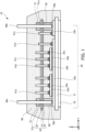
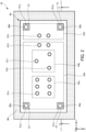
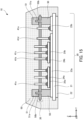
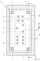
- FIG. 1 is a side cross-sectional view of a semiconductor device according to the first embodiment and FIG. 2 is a plan view of the semiconductor device according to the first embodiment. Note that FIG. 1 is a cross-sectional view along a dot-dash line X-X in FIG. 2.
- FIG. 2 is a plan view of a printed circuit board 30 from which an upper part of an encapsulating member 60 has been removed.
- the semiconductor device 10 includes an insulated circuit board 20, semiconductor chips 24a and 24b, the printed circuit board 30, external terminals 40a and 40b, and conductive posts 41a to 41e.
- the semiconductor device 10 further includes spacer portions 50 and pressing portions 51.
- these components are encapsulated by the encapsulating member 60.
- the semiconductor device 10 is encapsulated with the encapsulating member 60 so as to expose a rear surface of the insulated circuit board 20 (that is, a rear surface of a metal plate 22).
- the insulated circuit board 20 is rectangular in shape in plan view. Also in plan view, the insulated circuit board 20 has long sides that extend in the Y direction and short sides that extend in the X direction.
- the insulated circuit board 20 includes an insulating board 21, the metal plate 22 that is provided on a rear surface of the insulating board 21, and circuit patterns 23a and 23b provided on a front surface of the insulating board 21.
- the insulating board 21 and the metal plate 22 are rectangular in plan view. Corner portions of the insulating board 21 and the metal plate 22 may be chamfered into rounded or beveled shapes.
- the size of the metal plate 22 is smaller than the size of the insulating board 21 in plan view, and is formed inside the insulating board 21.
- the insulating board 21 is made of a ceramic or insulating resin with favorable thermal conductivity.
- Example ceramics include aluminum oxide, aluminum nitride, and silicon nitride.
- Example insulating resins include paper phenol board, paper epoxy board, glass composite board, and glass epoxy board.
- the metal plate 22 is made of metal with superior thermal conductivity.
- Example metals include aluminum, iron, silver, copper, or alloy containing at least one of such metals.
- the thickness of the metal plate 22 is 0.1 mm or more and 4.0 mm or less.
- a plating treatment may be performed on the surface of the metal plate 22 to improve corrosion resistance.
- the plating material in use may be nickel, nickel-phosphorus alloy, or nickel-boron alloy, for example.
- the circuit patterns 23a and 23b are made of a metal with superior electrical conductivity.
- Example metals include silver, copper, nickel, or alloy containing at least one of these metals.
- the thickness of the circuit patterns 23a and 23b is 0.1 mm or more and 4.0 mm or less.
- a plating treatment may be performed on the surfaces of the circuit patterns 23a and 23b to improve corrosion resistance. When doing so, the plating material in use may be nickel, nickel-phosphorus alloy, or nickel-boron alloy, for example.
- the circuit patterns 23a and 23b are formed as described below. As one example, the circuit patterns 23a and 23b may be obtained by forming a metal layer on the front surface of the insulating board 21 and subjecting this metal layer to a process such as etching.
- circuit patterns 23a and 23b that have been cut out from a metal layer in advance may be crimped onto the front surface of the insulating board 21.
- the circuit patterns 23a and 23b depicted in FIG. 1 are mere examples. The number, shapes, sizes, and the like of the circuit patterns may be selected as appropriate.
- a DCB (Direct Copper Bonding) board, an AMB (Active Metal Brazed) board, or a resin insulating board may be used.
- the semiconductor chips 24a and 24b are power devices made of silicon, silicon carbide, gallium nitride, or gallium oxide as a main component. These power devices are diode elements or switching elements.
- the semiconductor chip 24a includes a diode element.
- Example diodes include Schottky barrier diodes (SBDs) and free wheeling diodes (FWDs) such as PiN (P-intrinsic-N) diodes.
- This type of semiconductor chip 24a has an output electrode (or “cathode electrode”) as a main electrode on the rear surface and an input electrode (or “anode electrode”) as a main electrode on the front surface.
- the rear surface of the semiconductor chip 24a is bonded to the circuit pattern 23a by solder 25a.
- the conductive posts 41a are also mechanically and electrically connected to main electrodes on the front surface of the semiconductor chip 24a.
- the semiconductor chip 24b includes a switching element. Examples of a switching element include an IGBT and a power MOSFET.
- a switching element include an IGBT and a power MOSFET.
- the semiconductor chip 24b When the semiconductor chip 24b is an IGBT, the semiconductor chip 24b has a collector electrode as a main electrode on the rear surface, and a gate electrode as a control electrode and an emitter electrode as a main electrode on the front surface.
- the semiconductor chip 24b is a power MOSFET, the semiconductor chip 24b has a drain electrode as a main electrode on the rear surface and a gate electrode as a control electrode and a source electrode as a main electrode on the front surface.
- the rear surface of the semiconductor chip 24b described above is bonded to the circuit pattern 23a by solder 25b.
- the conductive post 41b and the conductive post 41c are mechanically and electrically connected to the main electrode and the control electrode, respectively, on the front surface of the semiconductor chip 24b.
- FIG. 1 merely depicts an example case where the semiconductor chips 24a and 24b are provided. The present disclosure is not limited to this case, and the number of semiconductor chips may be set according to the specification and the like of the semiconductor device 10.
- Lead-free solder is used for the solder 25a and 25b that bonds the semiconductor chips 24a and 24b and the circuit pattern 23a.
- the lead-free solder has at least one of an alloy made of tin-silver-copper, an alloy made of tin-zinc-bismuth, an alloy made of tin-copper, and an alloy made of tin-silver-indium-bismuth as a main component.
- the solder may further include additives.
- Example additives include nickel, germanium, cobalt, and silicon.
- Solder that contains additives has improved wettability, gloss, and bonding strength, which may improve reliability.
- Sintered metal may be used in place of the solder.
- the material of the sintered metal has silver or silver alloy as a main component.
- the printed circuit board 30 is provided facing the insulated circuit board 20 which is disposed horizontally. As depicted in FIG 1 , this printed circuit board 30 includes an insulating layer 31 and an upper circuit layer 32 formed on a front surface of the insulating layer 31. In addition, the printed circuit board 30 may have a lower circuit layer 33 on a rear surface of the insulating layer 31.
- the printed circuit board 30 is formed with the conductive posts 41a to 41e that pass through from the front surface to the rear surface. The conductive posts 41a to 41e are electrically connected to the upper circuit layer 32 and the lower circuit layer 33.
- the external terminals 40a and 40b are formed at locations on the printed circuit board 30 that face corner portions of the insulated circuit board 20. The external terminals 40a and 40b are electrically connected to the upper circuit layer 32 and the lower circuit layer 33.
- the insulating layer 31 is flat and made of an insulating material. This material is obtained by immersing a substrate in a resin.
- a resin paper, glass cloth, or glass non-woven fabric is used as the substrate.
- phenol resin, epoxy resin, or polyimide resin is used as the resin.
- Specific examples of the insulating layer 31 include a paper phenol substrate, a paper epoxy substrate, a glass epoxy substrate, a glass polyimide substrate, and a glass composite substrate.
- the insulating layer 31 is also rectangular in plan view. Corner portions of the insulating layer 31 may be chamfered into rounded or beveled shapes.
- the upper circuit layer 32 and the lower circuit layer 33 are patterned to form predetermined circuits. Note that the upper circuit layer 32 and the lower circuit layer 33 have been simply illustrated out of convenience as single layers in FIGS. 1 and 2 .
- the upper circuit layer 32 and the lower circuit layer 33 are made of a material with superior electrical conductivity. Example materials are silver, copper, nickel, or an alloy containing at least one of these metals.
- a plating treatment may be performed on the surfaces of the upper circuit layer 32 and the lower circuit layer 33 to improve corrosion resistance. Materials used in the plating treatment include nickel, nickel-phosphorus alloy, nickel-boron alloy, and the like.
- the printed circuit board 30 may be formed as described below.
- a metal foil is attached to each of the front and rear surfaces of the insulating layer 31 and resists of a predetermined shape are then printed.
- the metal foil on the front and rear surfaces of the insulating layer 31 is etched with the printed resists as masks, and any remaining resist is then removed.
- the upper circuit layer 32 and the lower circuit layer 33 are formed on the front and rear surfaces, respectively, of the insulating layer 31.
- a plurality of through-holes (not illustrated) are then formed by forming holes at predetermined positions in the laminate structure formed of the insulating layer 31, the upper circuit layer 32, and the lower circuit layer 33.
- a plating treatment may be performed on the plurality of through-holes to improve corrosion resistance. When doing so, as examples, solder plating or electroless gold plating is performed.
- a water-soluble flux treatment may also be performed.
- the external terminals 40a and 40b are press-fitted into the through-holes in the printed circuit board 30 so as to pass through. When doing so, the press-fitted locations are covered with solder.
- the external terminals 40a and 40b are then electrically connected to the upper circuit layer 32 and the lower circuit layer 33 of the printed circuit board 30. Lower end portions of the external terminals 40a and 40b are bonded via the solder 25c to the circuit patterns 23a and 23b of the insulated circuit board 20.
- the circuit patterns 23a and 23b of the insulated circuit board 20 may be provided with openings at attachment positions of the external terminals 40a and 40b, and the lower end portions of the external terminals 40a and 40b may be bonded via solder 25c to these openings.
- tube-shaped contact components may be bonded via solder to the attachment positions of the external terminals 40a and 40b of the circuit patterns 23a and 23b of the insulated circuit board 20 and the lower end portions of the external terminals 40a and 40b may be press-fitted into these contact components.
- the contact components in this case are made of a material with superior electrical conductivity.
- Example materials include silver, copper, nickel, or an alloy containing at least one of these metals.
- the external terminals 40a and 40b are cylindrical and are formed so as to be circular or rectangular in cross section.
- the external terminals 40a and 40b are made of a material with superior electrical conductivity.
- Example materials include silver, copper, nickel, or an alloy containing at least one of these metals.
- a plating treatment may be performed on the surfaces of the external terminals 40a and 40b to improve corrosion resistance.
- Example materials used in the plating treatment include nickel, nickel-phosphorus alloy, and nickel-boron alloy.
- the diameter (in the case of a circular cross section) or the length of a diagonal (in the case of a rectangular cross section) of the external terminals 40a and 40b is several percent longer than the diameter of the through-holes in the printed circuit board 30. This means that the external terminals 40a and 40b are press-fitted into the through-holes in the printed circuit board 30.
- the conductive posts 41a to 41e are press-fitted into the through-holes in the printed circuit board 30 so as to pass through. When doing so, the press-fitted locations are covered with solder (not illustrated).
- the lower end portions of the conductive posts 41a are bonded via the solder 25c to the main electrodes on the front surface of the semiconductor chip 24a.
- the lower end portions of the conductive posts 41b are bonded via the solder 25c to the main electrodes on the front surface of the semiconductor chip 24b.
- the lower end portion of the conductive post 41c is bonded via the solder 25c to the control electrode on the front surface of the semiconductor chip 24b.
- the lower end portions of the conductive posts 41d and 41e are bonded via the solder 25c to the circuit patterns 23a and 23b, respectively, of the insulated circuit board 20.
- These conductive posts 41a to 41e are column-shaped and are circular or rectangular in cross section.
- the lengths of the conductive posts 41a to 41e are sufficiently shorter than the lengths of the external terminals 40a and 40b.
- the conductive posts 41a to 41e are made of a material with superior electrical conductivity.
- Example materials include silver, copper, nickel, or an alloy containing at least one of these metals.
- a plating treatment may be performed on the surfaces of the conductive posts 41a to 41e to improve corrosion resistance.
- Example plating materials include nickel, nickel-phosphorus alloy, and nickel-boron alloy.
- the diameter (in the case of a circular cross section) or the length of a diagonal (in the case of a rectangular cross section) of the conductive posts 41a to 41e is several percent longer than the diameters of the through-holes in the printed circuit board 30. This means that the conductive posts 41a to 41e are press-fitted into the through-holes in the printed circuit board 30.
- Both the spacer portions 50 and the pressing portions 51 are made of a material that is resistant to heat and has a small coefficient of thermal expansion as a main component.
- Example materials include ceramics, carbon, and composite materials including ceramic and/or carbon.
- the spacer portions 50 are disposed at the four corners of the insulated circuit board 20 in plan view, and have the printed circuit board 30 disposed thereon. That is, the rear surfaces of the four corners of the printed circuit board 30 are respectively supported by the spacer portions 50.
- the spacer portions 50 are formed as polygonal prisms, and have through-holes 50a formed so as to pass through between the upper and lower surfaces of the spacer portions 50. This means that the external terminals 40a and 40b are inserted through the through-holes 50a in the spacer portions 50.
- the height from the lower surface to the upper surface of the spacer portions 50 corresponds to a desired distance of separation for the printed circuit board 30 from the insulated circuit board 20. So long as this height is maintained, the shape of the spacer portions 50 is not limited to a polygonal prism and may be a circular prism.
- the external terminals 40a and 40b do not need to be inserted through the spacer portions 50.
- the spacer portions 50 By inserting the external terminals 40a and 40b through the spacer portions 50, it is possible to dispose the spacer portions 50 in the limited space available above the insulated circuit board 20.
- the external terminals 40a and 40b into the through-holes 50a of the spacer portions 50, it is possible to suppress positional displacements of the printed circuit board 30, which is bonded to the external terminals 40a and 40b, in directions on a plane (the X-Y plane) . So long as the height is maintained, the spacer portions 50 do not need to be disposed at the four corners of the insulated circuit board 20.
- the spacer portions 50 may be disposed at the four corners of the insulated circuit board 20 even when the external terminals 40a and 40b are not provided at the four corners.
- support rods that are similar to the external terminals 40a and 40b may be provided at the four corners of the insulated circuit board 20 and the support rods may be inserted through the through-holes 50a in the spacer portions 50. By doing so, displacement of the spacer portion 50 in directions on a plane (the X-Y plane) may be suppressed.
- the pressing portions 51 are disposed on the spacer portions 50 with the printed circuit board 30 disposed in between. By doing so, the printed circuit board 30 may be pressed toward the spacer portions 50.
- the pressing portions 51 are formed as polygonal prisms and have through-holes 51a formed so as to pass through between the upper and lower surfaces of the pressing portions 51. This means that the external terminals 40a and 40b are inserted through the through-holes 51a in the pressing portions 51. It is sufficient for the height from the lower surface to the upper surface of the pressing portions 51 to be such that the height of the semiconductor device 10 is not exceeded when the pressing portions 51 are disposed on the printed circuit board 30. It is sufficient for the pressing portions 51 to be disposed on the spacer portions 50.
- the shape of the pressing portions 51 is not limited to a polygonal prism, and may be a circular prism. It is also sufficient for the pressing portions 51 to be disposed on the spacer portions 50, and the through-holes 51a are not indispensable.
- the external terminals 40a and 40b are not inserted through the spacer portions 50, the external terminals 40a and 40b are not inserted through the pressing portions 51 either.
- displacement of the pressing portion 51 in directions on a plane (the X-Y plane) may be suppressed. This makes it possible for the pressing portions 51 to reliably press the printed circuit board 30 onto the spacer portions 50.
- the pressing portions 51 are disposed at least above the spacer portions 50.
- the pressing portions 51 may be disposed as appropriate in such regions on the printed circuit board 30.
- the printed circuit board 30 is pressed by the spacer portions 50 and the pressing portions 51 through which the external terminals 40a and 40b have been inserted.
- the printed circuit board 30 is prevented from being positionally displaced in directions on a plane (the X-Y plane) and movement in the vertically upward direction (or Z direction) is also restricted. Since the printed circuit board 30 is kept in a substantially horizontal state, the state where the lower end portions of the conductive posts 41a to 41e are bonded to the front surfaces of the insulated circuit board 20 and to the semiconductor chips 24a and 24b is maintained. This will be further described later in this specification.
- the encapsulating member 60 contains thermosetting resin and a filler.
- thermosetting resins include epoxy resin, phenolic resin, and maleimide resin.
- An inorganic filler is used as the filler.
- inorganic fillers include silicon oxide, aluminum oxide, boron nitride, and aluminum nitride.
- the encapsulating member 60 contains an appropriate amount of a release agent. As examples, a wax-based, silicone-based, or fluorine-based release agent is used. Note that with the semiconductor device 10 that has been encapsulated in the encapsulating member 60, the metal plate 22 of the insulated circuit board 20 is exposed on the rear surface. When doing so, the metal plate 22 may be flush with the rear surface of the encapsulating member 60, or may protrude outward (in the -Z direction) from the rear surface.
- a cooling unit may be attached via a bonding member to the rear surface of the semiconductor device 10 described above.
- the bonding member used here is solder, brazing material, or sintered metal.
- Lead-free solder is used as the solder.
- Lead-free solder has an alloy containing at least two of tin, silver, copper, zinc, antimony, indium, and bismuth for example as a main component.
- the solder may additionally contain additives.
- Example additives include nickel, germanium, cobalt, and silicon.
- Solder that contains additives has improved wettability, gloss, and bonding strength, which may improve reliability.
- Example brazing materials have at least one of aluminum alloy, titanium alloy, magnesium alloy, zirconium alloy, and silicon alloy as a main component.
- the insulated circuit board 20 may be bonded by brazing using a bonding member like those described above.
- sintered metal has silver and silver alloy as a main component.
- the bonding member may be a thermal interface material.
- Thermal interface materials are adhesives including elastomer sheets, room temperature vulcanization (RTV) rubber, gels, phase change materials, and the like. Attaching a cooling unit via a brazing material or a thermal interface material like those described above improves the dissipation of heat by the semiconductor device 10.
- a cooling unit include a heat sink formed of a plurality of fins and a cooler device that uses water cooling.
- a heat sink is made of aluminum, iron, silver, or copper, which have superior thermal conductivity, or an alloy containing at least one of these metals. Also to improve corrosion resistance, as one example a material containing nickel as a main component may be formed by a plating treatment on the surface of the heat sink. As specific examples, aside from nickel, nickel-phosphorus alloy or nickel-boron alloy may be used.
- FIG. 3 is a flowchart of a method of manufacturing a semiconductor device according to the first embodiment.
- FIGS. 4 and 5 depict a mounting process included in the method of manufacturing the semiconductor device according to the first embodiment
- FIG. 6 depicts an attachment process included in the method of manufacturing the semiconductor device according to the first embodiment.
- a preparation process (step S1) is performed to prepare parts that construct the semiconductor device 10.
- the parts of the semiconductor device for example, the semiconductor chips 24a and 24b, the insulated circuit board 20, the external terminals 40a and 40b, the conductive posts 41a to 41e, the printed circuit board 30, the spacer portions 50, and the pressing portions 51 are prepared.
- the above parts are merely typical examples, and other parts aside from these are prepared as appropriate.
- an insulated circuit board assembly process (step S2a) is performed to set solder, the semiconductor chips 24a and 24b, and the like on the insulated circuit board 20, and a printed circuit board assembly process (step S2b) is performed to attach the external terminals 40a and 40b and the conductive posts 41a to 41e to the printed circuit board 30.
- a printed circuit board assembly process (step S2b) may be performed first.
- step S2a the semiconductor chips 24a and 24b are set via plate solder (not illustrated) in predetermined regions of the circuit pattern 23a of the insulated circuit board 20.
- plate solder is set in the regions of the circuit patterns 23a and 23b of the insulated circuit board 20 where the external terminals 40a and 40b and the conductive posts 41a to 41e are to be bonded.
- step S2b the external terminals 40a and 40b and the conductive posts 41a to 41e may be inserted through predetermined through-holes in the printed circuit board 30 bonded using solder (see the upper part of FIG. 4 ).
- step S3 a mounting process (step S3) is performed to mount the printed circuit board 30 on the insulated circuit board 20 obtained in steps S2a and S2b.
- the spacer portions 50 are disposed so that the through-holes 50a correspond to the areas of the circuit pattern 23a of the insulated circuit board 20 assembled in step S2a where the external terminals 40a and 40b are to be bonded.
- the printed circuit board 30 assembled in step S2b is mounted on the insulated circuit board 20 on which the spacer portions 50 have been disposed.
- the external terminals 40a and 40b provided on the printed circuit board 30 are aligned with the through-holes 50a of the spacer portions 50, as depicted in FIG. 4 .
- the lower end portions of the conductive posts 41a to 41e of the printed circuit board 30 are aligned with the semiconductor chips 24a and 24b and the circuit patterns 23a and 23b on which the plate solder has been disposed.
- the lower end portions of the external terminals 40a and 40b and the conductive posts 41a to 41e are placed in contact with the insulated circuit board 20 and the semiconductor chips 24a and 24b.
- the external terminals 40a and 40b are inserted through the through-holes 50a of the spacer portions 50.
- the rear surfaces of the four corners of the printed circuit board 30 are maintained by the spacer portions 50.
- step S4 an attachment process is performed to attach the pressing portions 51 to the external terminals 40a and 40b which extend vertically upward (in the +Z direction) from the front surface of the printed circuit board 30.
- the external terminals 40a and 40b that extend vertically upward (in the +Z direction) from the front surface of the printed circuit board 30 are inserted through the through-holes 51a of the pressing portions 51.
- the pressing portions 51 become attached to the spacer portions 50 with the printed circuit board 30 disposed in between.
- step S5 a solder bonding process (step S5) is performed to add heat to melt the solder and then perform cooling to create solder bonds.
- step S4 the insulated circuit board 20 to which the printed circuit board 30 has been attached is heated at a predetermined temperature to melt the plate solder.
- warping of the printed circuit board 30 may occur due to a difference in linear expansion coefficients between the insulating layer 31 and the upper circuit layer 32 and lower circuit layer 33.
- the printed circuit board 30 is pressed toward the spacer portions 50 by the pressing portions 51. By doing so, the warping that has occurred in the printed circuit board 30 is corrected, and the printed circuit board 30 is kept substantially horizontal.
- the lower end portions of the conductive posts 41a to 41e do not become separated from the insulated circuit board 20 and the semiconductor chips 24a and 24b and are maintained in a state where the lower end portions of the conductive posts 41a to 41e contact the insulated circuit board 20 and the semiconductor chips 24a and 24b as depicted in FIG. 6 .
- the external terminals 40a and 40b and the conductive posts 41a to 41e are reliably bonded mechanically and electrically to the insulated circuit board 20 and the semiconductor chips 24a and 24b.
- step S6 an encapsulating process is performed to encapsulate the printed circuit board 30, to which the external terminals 40a and 40b have been attached, and the insulated circuit board 20 and the semiconductor chips 24a and 24b, to which the conductive posts 41a to 41e have been bonded, with the encapsulating member.
- the printed circuit board 30, the insulated circuit board 20, and the semiconductor chips 24a and 24b that were integrated in step S5 are set in a predetermined mold and the mold is filled with the encapsulating member. When the encapsulating member has solidified, the structure is released from the mold to obtain the semiconductor device 10 depicted in FIGS. 1 and 2 .
- the semiconductor device 10 described above includes: the semiconductor chips 24a and 24b that have electrodes on their main surfaces; the insulated circuit board 20 that includes the insulating board 21 and the circuit patterns 23a and 23b formed on the front surface of the insulating board 21; the conductive posts 41a to 41e whose lower end portions are bonded to the circuit patterns 23a and 23b and the front surfaces of the semiconductor chips 24a and 24b and whose upper end portions extend vertically upward with respect to the circuit patterns 23a and 23b and the front surfaces of the semiconductor chips 24a and 24b; and the printed circuit board 30 that is bonded to the upper end portion-sides of the conductive posts 41a to 41e and disposed facing the insulated circuit board 20.
- the printed circuit board 30 is disposed facing the insulated circuit board 20 with the spacer portions 50 disposed in between on the front surface of the insulated circuit board 20, and the pressing portions 51 are disposed on the spacer portions 50 with the printed circuit board 30 disposed in between.
- the pressing portions 51 are able to correct warping of the printed circuit board 30 that occurs due to heating performed to bond the conductive posts 41a to 41e to the insulated circuit board 20 and the semiconductor chips 24a and 24b.
- the lower end portions of the conductive posts 41a to 41e do not become separated from the insulated circuit board 20 and the semiconductor chips 24a and 24b and remain mechanically and electrically bonded to the insulated circuit board 20 and the semiconductor chips 24a and 24b.
- the mechanical and electrical connections of the conductive posts 41a to 41e are maintained and deterioration in the reliability of the semiconductor device 10 is suppressed.
- the shape, disposed positions, and number of the pressing portions 51 are not limited to the example depicted in FIGS. 1 and 2 .
- modifications to the pressing portions 51 that differ from the configuration depicted in FIGS. 1 and 2 will be described.
- the main difference from the semiconductor device 10 in FIGS. 1 and 2 is the pressing portions 51.
- the description will mainly focus on parts that are different from the semiconductor device 10 in FIGS. 1 and 2 .
- Other parts that do not differ are as described with reference to FIGS. 1 and 2 .
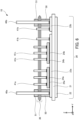
- FIG. 7 is a side cross-sectional view of the semiconductor device according to Modification 1-1 of the first embodiment
- FIG. 8 is a plan view of the semiconductor device according to Modification 1-1 of the first embodiment. Note that FIG. 7 is a cross-sectional view taken along the dot-dash line X-X in FIG. 8.
- FIG. 8 is a plan view of the printed circuit board 30 with an upper portion of the encapsulating member 60 in FIG. 7 removed.
- the pressing portions 51 are I-shaped and have a length corresponding to the long sides of the insulated circuit board 20.
- the pressing portions 51 are provided along the facing long sides of the insulated circuit board 20, and have the external terminals 40a and 40b inserted through the through-holes 51a provided at both ends.
- the pressing portions 51 of Modification 1-1 have a wider area for pressing the printed circuit board 30 than the pressing portions 51 in FIGS. 1 and 2 . This means that the pressing portions 51 of Modification 1-1 may more reliably correct warping of the printed circuit board 30 than the pressing portions 51 in FIGS. 1 and 2 . Accordingly, it is possible to more reliably prevent the separation of the conductive posts 41a to 41e from the insulated circuit board 20 and the semiconductor chips 24a and 24b.
- the spacer portions 50 it is also preferable for the spacer portions 50 to be disposed below the pressing portion 51 to the greatest degree possible.
- the encapsulating member is filled from a side portion of the insulated circuit board 20.
- the spacer portions 50 are shaped and placed so as not to block filling paths taken by the encapsulating member.
- the spacer portions 50 it is preferable that the spacer portions 50 to be disposed at locations facing the four corners of the printed circuit board 30 as depicted in FIGS. 1 and 2 and described in the first embodiment.
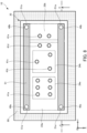
- FIG. 9 is a plan view of a semiconductor device according to Modification 1-2 of the first embodiment. Note that FIG. 1 may be referred to as a cross-sectional view taken along the dot-dash line X-X in FIG. 9. FIG. 9 is a plan view of the printed circuit board 30 with an upper portion of the encapsulating member 60 removed.
- the pressing portions 51 are I-shaped and have a length corresponding to the short sides of the insulated circuit board 20.
- the pressing portions 51 are provided along the facing short sides of the insulated circuit board 20, and have the external terminals 40a and 40b inserted through the through-holes 51a at both ends.
- the pressing portions 51 of Modification 1-2 also have a wider area for pressing the printed circuit board 30 than the pressing portions 51 of FIGS. 1 and 2 . This means that the pressing portions 51 of Modification 1-2 may more reliably correct warping of the printed circuit board 30 than the pressing portions 51 in FIGS. 1 and 2 . Accordingly, it is possible to more reliably prevent separation of the conductive posts 41a to 41e from the insulated circuit board 20 and the semiconductor chips 24a and 24b.
- FIG. 10 is a plan view of a semiconductor device according to Modification 1-3 of the first embodiment. Note that FIG. 7 may be referred to as a cross-sectional view taken along the dot-dash line X-X in FIG. 10.
- FIG. 10 is a plan view of the printed circuit board 30 with an upper portion of the encapsulating member 60 removed.
- a pressing portion 51 is formed in a continuous ring shape in plan view and has dimensions corresponding to the long sides and short sides of the insulated circuit board 20.
- the pressing portion 51 is provided along the long and short sides of the insulated circuit board 20 and has the external terminals 40a and 40b inserted through through-holes 51a at the four corners.
- the pressing portion 51 of Modification 1-3 has a wider area for pressing the printed circuit board 30 than the pressing portions 51 in FIGS. 1 and 2 and in Modifications 1-1 and 1-2. This means that the pressing portion 51 of Modification 1-3 may more reliably correct the warping of the printed circuit board 30. Accordingly, it is possible to more reliably prevent the separation of the conductive posts 41a to 41e from the insulated circuit board 20 and the semiconductor chips 24a and 24b.
- a ring-shaped pressing portion 51 may have parts that cross the facing long sides and the facing short sides so as to avoid interference with the conductive posts 41a to 41e on the front surface of the printed circuit board 30.
- FIG. 11 is a side cross-sectional view of the semiconductor device according to Modification 1-4 of the first embodiment
- FIG. 12 is a plan view of the semiconductor device according to Modification 1-4 of the first embodiment. Note that FIG. 11 is a cross-sectional view taken along the dot-dash line X-X in FIG. 12.
- FIG. 12 is a plan view of the printed circuit board 30 with an upper portion of the encapsulating member 60 in FIG. 11 removed.
- the pressing portions 51 in the semiconductor device 10 in FIGS. 1 and 2 are not provided, and pressing members 40a1 and 40b1 are formed on outer peripheral surfaces of the external terminals 40a and 40b.
- the pressing members 40a1 and 40b1 protrude outward from the outer peripheral surfaces of the external terminals 40a and 40b perpendicularly (that is, on an X-Y plane) to the direction (or " ⁇ Z direction") in which the external terminals 40a and 40b extend.
- the pressing members 40a1 and 40b1 protrude outward in four directions from the outer peripheral surfaces of the external terminals 40a and 40b in plan view.
- the external terminals 40a and 40b are prepared in advance in step S1 in FIG. 3 , and once the mounting process (step S3 in FIG. 3 ) of mounting the printed circuit board 30, to which the external terminals 40a and 40b have been attached, on the insulated circuit board 20 has been performed, the printed circuit board 30 is pressed toward the spacer portions 50 by the pressing members 40a1 and 40b1. This means that warping of the printed circuit board 30 may be corrected without performing step S4 in FIG. 3 (that is, without using the pressing portions 51).
- the semiconductor device 10 according to Modification 1-4 may be manufactured without using the pressing portions 51 and with fewer manufacturing processes compared to FIGS. 1 and 2 and Modifications 1-1 to 1-3, which may reduce the manufacturing cost.
- the pressing members 40a1 and 40b1 of the external terminals 40a and 40b may be performed on the external terminals 40a and 40b to cause the pressing members 40a1 and 40b1 to protrude outward.
- the pressing members 40a1 and 40b1 may be bonded to the external terminals 40a and 40b by welding. It is sufficient for the pressing members 40a1 and 40b1 to press the printed circuit board 30 toward the spacer portions 50. For this reason, the shape of the pressing members 40a1 and 40b1 is not limited to the shape depicted in FIG. 12 .
- two or more pressing members 40a1 and 40b1 may be formed around the outer periphery on the outer peripheral surfaces of the external terminals 40a and 40b at equal intervals in plan view.
- the pressing members 40a1 and 40b1 may be formed in ring shapes or fan shapes around the outer periphery of the outer peripheral surfaces of the external terminals 40a and 40b in plan view.
- the lengths of the pressing members 40a1 and 40b1 formed on the external terminals 40a and 40b do not need to be isotropic. Since the external terminals 40a and 40b are provided at the four corners of the printed circuit board 30, the lengths of the pressing members 40a1 and 40b1 that face the outside of the printed circuit board 30 from the external terminals 40a and 40b are limited so as not to protrude outside the printed circuit board 30. On the other hand, the pressing members 40a1 and 40b1 that face the inside of the printed circuit board 30 from the external terminals 40a and 40b may be longer than the pressing members 40a1 and 40b1 that face the outside.
- FIG. 13 is a side cross-sectional view of the semiconductor device according to Modification 1-5 of the first embodiment
- FIG. 14 is a plan view of the semiconductor device according to Modification 1-5 of the first embodiment. Note that FIG. 13 is a cross-sectional view taken along the dot-dash line X-X in FIG. 14.
- FIG. 14 is a plan view of the printed circuit board 30 with an upper portion of the encapsulating member 60 in FIG. 13 removed.
- the semiconductor device 10 according to Modification 1-5 does not use the pressing portions 51 in the semiconductor device 10 in FIGS. 1 and 2 and instead has wedge members 40a2 and 40b2 inserted around the external terminals 40a and 40b in the through-holes 30a of the printed circuit board 30 through which the external terminals 40a and 40b have been inserted.
- the diameters of the through-holes 30a are formed several percent larger than the diameter of the through-holes in the printed circuit board 30 in FIGS. 1 and 2 through which the external terminals 40a and 40b are inserted.
- the wedge members 40a2 and 40b2 are tube shaped.
- the inner diameters of the wedge members 40a2 and 40b2 may be the same as or several percent smaller than the diameters of the external terminals 40a and 40b.
- the outer diameter of the wedge members 40a2 and 40b2 (that is, the diameter of the outer surface in plan view) may be the same as the diameter of the through-holes 30a in the printed circuit board 30 or several percent larger.
- the diameters of the outer surfaces of the wedge members 40a2 and 40b2 may also decrease in the -Z direction. By doing so, it becomes easier to insert the wedge members 40a2 and 40b2 into the gaps between the external terminals 40a and 40b and the through-holes 30a and 30b.
- flanges are integrally formed on front surface-sides of the wedge members 40a2 and 40b2. Each flange may be sized so as not to protrude from the front surface of the printed circuit board 30 when the wedge members 40a2 and 40b2 have been attached.
- the wedge members 40a2 and 40b2 are also made of a material that is resistant to heat and has a small coefficient of thermal expansion as a main component.
- Example materials include ceramics, carbon, and composite materials including ceramic and/or carbon.
- step S1 of FIG. 3 the wedge members 40a2 and 40b2 are also prepared as parts that form the semiconductor device 1.
- step S2b of FIG. 3 the external terminals 40a and 40b are inserted through the through-holes 30a of the printed circuit board 30.
- the wedge members 40a2 and 40b2 are inserted onto the external terminals 40a and 40b and driven between the external terminals 40a and 40b and the through-holes 30a.
- the external terminals 40a and 40b are fixed to the printed circuit board 30 by the wedge members 40a2 and 40b2.
- step S3 of FIG. 3 the printed circuit board 30 is mounted on the insulated circuit board 20.
- the lower end portions of the external terminals 40a and 40b fixed to the printed circuit board 30 are inserted through the through-holes 50a of the spacer portions 50 and come into contact with the front surface of the insulated circuit board 20.
- the printed circuit board 30 is fixed to the external terminals 40a and 40b, and the front surface of the printed circuit board 30 is pressed toward the spacer portions 50 by the flanges of the wedge members 40a2 and 40b2.
- step S5 is performed without performing step S4 in FIG. 3 (that is, without using the pressing portions 51). Since the front surface of the printed circuit board 30 is pressed toward the spacer portions 50 by the flanges of the wedge members 40a2 and 40b2, warping of the printed circuit board 30 caused by heating may be corrected. Since the printed circuit board 30 is kept horizontal, the lower end portions of the conductive posts 41a to 41e do not become separated from the insulated circuit board 20 and the semiconductor chips 24a and 24b, so that the lower end portions are reliably bonded in a state where contact between the lower end portions and the insulated circuit board 20 and the semiconductor chips 24a and 24b is maintained. After this, the encapsulating process of step S6 in FIG. 3 is performed to obtain the semiconductor device 10 depicted in FIGS. 13 and 14 .
- the semiconductor device 10 according to Modification 1-5 may be manufactured without using the pressing portions 51 and with fewer manufacturing processes, which may reduce the manufacturing cost.
- FIG. 15 is a side cross-sectional view of the semiconductor device according to Modification 1-6 of the first embodiment
- FIG. 16 is a plan view of the semiconductor device according to Modification 1-6 of the first embodiment. Note that FIG. 15 is a cross-sectional view taken along the dot-dash line X-X in FIG. 16.
- FIG. 16 is a plan view of the printed circuit board 30 with an upper portion of the encapsulating member 60 in FIG. 15 removed.
- convex portions 50b that extend vertically upward (in the +Z direction) with respect to the front surface of the insulated circuit board 20 are formed on the upper surfaces of the spacer portions 50 that face the pressing portions 51.
- Through-holes (not illustrated) at the four corners of the printed circuit board 30 are disposed on the spacer portions 50, with the convex portions 50b inserted therethrough.
- the convex portions 50b may be circular prisms or polygonal prisms. The convex portions 50b need to be longer than the thickness of the printed circuit board 30.
- the through-holes 51a are formed in the lower surfaces of the pressing portions 51 that face the spacer portions 50.
- the through-holes 51a have shapes and sizes corresponding to the convex portions 50b.
- the through-holes 51a may pass through from the rear surface to the front surface of the pressing portions 51, as depicted in FIG. 1 , or do not need to pass through the front surface, as depicted in FIG. 15 .
- the convex portions 50b that protrude from the front surface of the printed circuit board 30 are fitted into the through-holes 51a of the pressing portions 51, so that the printed circuit board 30 is interposed between the pressing portions 51 and the spacer portions 50.
- step S1 of FIG. 3 the spacer portions 50 provided with the convex portions 50b and the pressing portions 51 in which the through-holes 51a are formed are prepared. Note that the external terminals 40a and 40b are not included in this configuration.
- step S3 in FIG. 3 the printed circuit board 30 that was assembled in step S2b is mounted via the spacer portions 50 on the insulated circuit board 20.
- the convex portions 50b of the spacer portions 50 are passed through the four corners of the printed circuit board 30, and the lower end portions of the conductive posts 41a to 41e of the printed circuit board 30 are mounted on the semiconductor chips 24a and 24b and the circuit patterns 23a and 23b on which plate solder has been disposed.
- step S4 of FIG. 3 the convex portions 50b that protrude from the printed circuit board 30 are inserted into the through-holes 51a to attach the pressing portions 51 onto the spacer portions 50 with the printed circuit board 30 in between. Since convex portions 51b of the spacer portions 50 are inserted through the printed circuit board 30, movement of the printed circuit board 30 in directions on a plane (the X-Y plane) is restricted. Since the printed circuit board 30 is interposed between the pressing portions 51 and the spacer portions 50, movement in the vertical direction ( ⁇ Z direction) is also restricted. Next, the processing in step S5 in FIG. 3 is performed.
- step S6 in FIG. 3 is performed to obtain the semiconductor device 10 in FIGS. 15 and 16 .
- the semiconductor device 10 according to Modification 1-6 does not include the external terminals 40a and 40b, since the convex portions 50b are formed in the spacer portions 50 and the through-holes 51a are formed in the pressing portions 51, warping of the printed circuit board 30 is corrected and it is possible to maintain the contact between the lower end portions of the conductive posts 41a to 41e and the insulated circuit board 20 and the semiconductor chips 24a and 24b. As a result, the mechanical and electrical connections of the conductive posts 41a to 41e are maintained, and deterioration in the reliability of the semiconductor device 10 is suppressed.
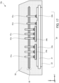
- FIG. 17 is a side cross-sectional view of the semiconductor device according to the second embodiment
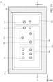
- FIG. 18 is a plan view of the semiconductor device according to the second embodiment.
- a semiconductor device 10a includes the insulated circuit board 20, the semiconductor chips 24a and 24b, the printed circuit board 30, and the conductive posts 41a to 41e. Also, unlike the semiconductor device 10 according to the first embodiment, the semiconductor device 10a does not include the external terminals 40a and 40b, the spacer portions 50, and the pressing portions 51.
- the components of the semiconductor device 10a are encapsulated by the encapsulating member 60.
- the semiconductor device 10a is also encapsulated with the encapsulating member 60 so as to expose the rear surface of the insulated circuit board 20 (that is, the rear surface of the metal plate 22).
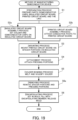
- FIG. 19 is a flowchart of a method of manufacturing a semiconductor device according to the second embodiment.
- FIGS. 20 and 21 depict a mounting process included in the method of manufacturing the semiconductor device according to the second embodiment
- FIG. 22 depicts an attachment process included in the method of manufacturing the semiconductor device according to the second embodiment. Note that the description will focus on processes that differ from the method of manufacturing in FIG. 3 of the first embodiment.
- a preparation process (step S1) is performed to prepare parts that construct the semiconductor device 10.
- the semiconductor chips 24a and 24b, the insulated circuit board 20, the conductive posts 41a to 41e, the printed circuit board 30, the spacer portions 50, the pressing portions 51, and the like are prepared.
- an insulated circuit board assembly process (step S2a) is performed to dispose solder, semiconductor chips 24a and 24b, and the like on the insulated circuit board 20 and a printed circuit board assembly process (step S2b) is performed to attach the conductive posts 41a to 41e to the printed circuit board 30.
- a printed circuit board assembly process (step S2b) may be performed first.
- the insulated circuit board 20 is set inside a mold 70 and the semiconductor chips 24a and 24b are disposed via plate solder (not illustrated) in predetermined regions of the circuit pattern 23a of the insulated circuit board 20.
- Plate solder is disposed in the same way in regions of the circuit patterns 23a and 23b of the insulated circuit board 20 and the semiconductor chips 24a and 24b where the conductive posts 41a to 41e are to be bonded.
- the spacer portions 50 are disposed at the four corners of the insulated circuit board 20.
- the conductive posts 41a to 41e may be inserted through predetermined through-holes in the printed circuit board 30 and bonded by solder.
- step S3 a mounting process (step S3) is performed to mount the printed circuit board 30 on the insulated circuit board 20 obtained in steps S2a and S2b.
- the printed circuit board 30 assembled in step S2b is mounted on the insulated circuit board 20 assembled in step S2a.
- the printed circuit board 30 is disposed on the spacer portions 50, and the lower end portions of the conductive posts 41a to 41e on the printed circuit board 30 are placed in contact with the semiconductor chips 24a and 24b and the circuit patterns 23a and 23b on which plate solder has been disposed.
- step S4 an attachment process is performed to attach the pressing portions 51 to the front surface of the printed circuit board 30 (step S4).
- the pressing portions 51 are attached to the spacer portions 50 with the printed circuit board 30 disposed in between. Since the printed circuit board 30 is interposed between the pressing portions 51 and the spacer portions 50, movement in the vertical direction (in the ⁇ Z direction) is restricted.
- step S5 a solder bonding process is performed to add heat to melt the solder and then perform cooling to create solder bonds.
- the printed circuit board 30 is pressed toward the spacer portions 50 by the pressing portions 51.
- the warping of the printed circuit board 30 is corrected, and the lower end portions of the conductive posts 41a to 41e are kept in contact with the insulated circuit board 20 and the semiconductor chips 24a and 24b.
- the external terminals 40a and 40b and the conductive posts 41a to 41e are reliably bonded to the insulated circuit board 20 and the semiconductor chips 24a and 24b.
- step S6a a removing process is performed to remove the spacer portions 50 and the pressing portions 51 from the printed circuit board 30, the insulated circuit board 20, and the semiconductor chips 24a and 24b which are integrated.
- the printed circuit board 30, the insulated circuit board 20, and the semiconductor chips 24a and 24b that are integrated are removed from the mold 70 when removing the spacer portions 50 and the pressing portions 51.
- the pressing portions 51 are pulled upward to remove the spacer portions 50 to the outside.
- step S6 an encapsulating process is performed to encapsulate the printed circuit board 30, the insulated circuit board 20, and the semiconductor chips 24a and 24b that have been integrated with an encapsulating member.
- the printed circuit board 30, the insulated circuit board 20 and the semiconductor chips 24a and 24b that have been integrated and from which the spacer portions 50 and the pressing portions 51 have been removed in step S6a are set in a predetermined mold and the inside of the mold is filled with the encapsulating member.
- the mold is released to obtain the semiconductor device 10a depicted in FIGS. 17 and 18 .
- warping that occurs in the printed circuit board 30 during the heating included in the manufacturing process may be corrected by the pressing portions 51. That is, since the printed circuit board 30 is kept substantially horizontal, the lower end portions of the conductive posts 41a to 41e do not become separated from the insulated circuit board 20 and the semiconductor chips 24a and 24b and therefore remain bonded to the insulated circuit board 20 and the semiconductor chips 24a and 24b. As a result, the mechanical and electrical connections of the conductive posts 41a to 41e are maintained, thereby suppressing deterioration in the reliability of the semiconductor device 10a.
- FIGS. 23 and 24 depict a mounting process included in the method of manufacturing the semiconductor device according to the third embodiment.
- steps S1, S2a, and S2b in FIG. 19 are performed in the same way as in the second embodiment. Note that spacer portions 55 and pressing portions 56, which are additionally prepared in step S1, will be described later.
- the insulated circuit board 20 is set in the mold 70 and the semiconductor chips 24a and 24b are disposed via plate solder (not illustrated) in predetermined regions of the circuit pattern 23a of the insulated circuit board 20.
- the insulated circuit board 20 is set in the mold 70 with a gap provided on the left side in FIG. 23 .
- Plate solder is disposed in the same way in regions of the circuit patterns 23a and 23b of the insulated circuit board 20 and the semiconductor chips 24a and 24b where the conductive posts 41a to 41e are to be bonded.
- the spacer portions 50 and 55 are disposed at the four corners of the insulated circuit board 20.
- the spacer portions 50 are disposed on the right side of the insulated circuit board 20 in FIG. 23 (at the front and behind relative to the plane of the drawing). Note that concave portions 50c are formed on the upper surfaces of the spacer portions 50.
- the spacer portions 55 have convex portions 55a that extend vertically downward (in the -Z direction) relative to rear surfaces of the spacer portions 50 formed at end portions of the rear surface.
- each spacer portion 55 has a concave portion 55b formed on the upper surface above the convex portion 55a. Accordingly, the spacer portions 55 are disposed on the left of the insulated circuit board 20 in FIG. 23 (at the front and behind relative to the plane of the drawing), with the convex portions 55a fitting between the insulated circuit board 20 and the mold 70.
- step S3 a mounting process (step S3) is performed to mount the printed circuit board 30 on the insulated circuit board 20 obtained in steps S2a and S2b.
- the printed circuit board 30 assembled in step S2b is mounted on the spacer portions 50 and 55 of the insulated circuit board 20 assembled in step S2a.
- an attachment process is performed to attach the pressing portions 51 and 56 to the front surface of the printed circuit board 30 (step S4).
- the pressing portions 51 are attached onto the spacer portions 50 on the right side in FIG. 24 with the printed circuit board 30 disposed in between.
- the convex portions 51b are formed on the lower surfaces of the pressing portions 51.
- the convex portions 51b pass through the printed circuit board 30 and fit into the concave portions 50c of the spacer portions 50.
- the pressing portions 56 are attached onto the spacer portions 55 on the left side in FIG. 24 with the printed circuit board 30 disposed in between.
- the pressing portions 56 have convex portions 56a that extend vertically downward (in the -Z direction) relative to rear surfaces of the pressing portions 51 formed at end portions of the rear surface.
- the pressing portions 56 are formed with throughholes 56b that pass through from the upper surfaces to the lower surfaces of the convex portions 56a.
- These pressing portions 56 are attached to the left side in FIG. 24 of the printed circuit board 30 with the convex portions 56a fitting between the printed circuit board 30 and the mold 70.
- support rods 56c are passed through the throughholes 56b in the pressing portions 56 and are inserted into concave portions 55b in the spacer portions 55.
- the printed circuit board 30 is interposed between the pressing portions 51 and 56 and the spacer portions 50 and 55. This means that movement of the printed circuit board 30 in the vertical direction ( ⁇ Z direction) is restricted. In addition, movement of the printed circuit board 30 in directions on a plane (the X-Y plane) is restricted by the convex portions 56a of the pressing portions 56 as well as the support rods 56c, and the convex portions 51b of the pressing portions 51.
- step S5 a solder bonding process is performed to add heat to melt the solder and then perform cooling to create soldered bonds.
- the printed circuit board 30 is pressed toward the spacer portions 50 and 55 by the pressing portions 51 and 56. This means that the warping that has occurred for the printed circuit board 30 is corrected and the lower end portions of the conductive posts 41a to 41e are kept in contact with the insulated circuit board 20 and the semiconductor chips 24a and 24b.
- the conductive posts 41a to 41e are reliably bonded to the insulated circuit board 20 and the semiconductor chips 24a and 24b.
- step S6a a removing process is performed to remove the pressing portions 51 and 56 and the spacer portions 50 and 55 from the integrated printed circuit board 30, the insulated circuit board 20 and the semiconductor chips 24a and 24b.
- a removing process is performed to remove the pressing portions 51 and 56 and the spacer portions 50 and 55 from the integrated printed circuit board 30, the insulated circuit board 20 and the semiconductor chips 24a and 24b.
- step S6 an encapsulating process is performed to encapsulate the printed circuit board 30, the insulated circuit board 20, and the semiconductor chips 24a and 24b that have been integrated with an encapsulating member.
- step S6a the pressing portions 51 and 56 and the spacer portions 50 and 55 are removed, and the printed circuit board 30, the insulated circuit board 20 and the semiconductor chips 24a and 24b that have been integrated are set in a predetermined mold, which is then filled with the encapsulating member.
- the mold is released to obtain the semiconductor device 10a depicted in FIGS. 17 and 18 .
- the pressing portions 51 and 56 are able to prevent the printed circuit board 30 from becoming displaced in directions on a plane.
- the lower end portions of the conductive posts 41a to 41e do not become separated from the insulated circuit board 20 and the semiconductor chips 24a and 24b, do not become positionally displaced, and remain bonded to the insulated circuit board 20 and the semiconductor chips 24a and 24b.
- the mechanical and electrical connections of the conductive posts 41a to 41e are maintained, which suppress deterioration in the reliability of the semiconductor device 10a.
Landscapes
- Engineering & Computer Science (AREA)
- Microelectronics & Electronic Packaging (AREA)
- Manufacturing & Machinery (AREA)
- Combinations Of Printed Boards (AREA)
- Structures For Mounting Electric Components On Printed Circuit Boards (AREA)
Abstract
Description
- The embodiments discussed herein relate to a semiconductor device and a method of manufacturing a semiconductor device.
- A semiconductor device is equipped with semiconductor chips including power devices, and is used as a power converter apparatus. The power devices are switching elements. Example switching elements include insulated gate bipolar transistors (IGBTs) and power metal oxide semiconductor field effect transistors (MOSFETs).
- This type of semiconductor device includes an insulated circuit board, a semiconductor chip, and a printed circuit board. The insulated circuit board includes an insulating board and a plurality of circuit patterns provided on the insulating board. Semiconductor chips are provided on predetermined circuit patterns. The printed circuit board includes predetermined circuit layers. Conductive posts are press-fitted into and passed through through-holes in the printed circuit board. The conductive posts attached to a printed circuit board are bonded to the circuit patterns on the insulated circuit board and also to the semiconductor chips. The insulated circuit board, the printed circuit board, and the semiconductor chips that have been integrated in this way are set in a mold and resin is injected into the mold interior to encapsulate the components, thereby manufacturing a semiconductor device (as examples, see
PTL 1 to 5). Alternatively, a printed circuit board may be bonded to external terminals that extend from a semiconductor device in which an insulated circuit board and semiconductor chips have been encapsulated in resin, and a power module, a printed circuit board, and a heat sink may be screwed on (seePTL 6 for example). - It is also possible to regard the type of semiconductor device described above as a "unit", to dispose a plurality of these units on a cooler, to provide a wiring board on the front side of the plurality of units, and to bolt the wiring board and the cooler together (see, for example, PTL 7). A printed circuit board may also be fixed to a compound resin structure using screws (see, for example, PTL 8).
-
- PTL 1:
Japanese Laid-open Patent Publication No. 2014-154806 - PTL 2:
Japanese Laid-open Patent Publication No. 2020-136293 - PTL 3: International Publication Pamphlet No.
WO 2015/151235 - PTL 4:
Japanese Laid-open Patent Publication No. 2010- 165764 - PTL 5: International Publication Pamphlet No.
WO 2015/064231 - PTL 6:
Japanese Laid-open Patent Publication No. 2019- 140315 - PTL 7:
Japanese Laid-open Patent Publication No. 2013-191806 - PTL 8: International Publication Pamphlet No.
WO 2009/069308 - However, in a semiconductor device, when heating is performed to bond the conductive posts attached to a printed circuit board to the circuit patterns of the insulated circuit board and the semiconductor chips with solder, warping of the printed circuit board may occur. As a result, the conductive posts may become separated from the circuit patterns and the semiconductor chips, which prevents mechanical and electrical connections from being made. A semiconductor device manufactured in this way has low reliability and, in some cases, may be defective.
- The present disclosure was conceived in view of the problem described above and it is an object of the present disclosure to provide a semiconductor device and a method of manufacturing a semiconductor device where the mechanical and electrical connections of conductive posts are reliable.
- According to an aspect, there is provided a semiconductor device including: a semiconductor chip provided with an electrode on a main surface thereof; an insulated circuit board including an insulating board and a circuit pattern that is formed on a front surface of the insulating board and has the semiconductor chip disposed thereupon; a plurality of conductive posts whose lower end portions are bonded to at least one of the front surface of the circuit pattern and the electrode of the semiconductor chip, and whose upper end portions extend vertically upward with respect to a front surface of the insulated circuit board; and a printed circuit board that is bonded to upper end portion-sides of the conductive posts and is disposed facing the insulated circuit board, wherein the printed circuit board is disposed facing the insulated circuit board with a spacer in between on a front surface of the insulated circuit board, and a pressing portion is disposed above the spacer portion with the printed circuit board in between.
- According to another aspect, there is provided a method of manufacturing a semiconductor device including: a preparation step of preparing a semiconductor chip provided with an electrode on a main surface, an insulating a circuit board including an insulating board and a circuit pattern formed on a front surface of the insulating board, a plurality of conductive posts, and a printed circuit board; a mounting step of placing the printed circuit board facing the insulated circuit board via a spacer portion on a front surface of the insulated circuit board, and disposing lower end portions of the plurality of conductive posts, which have been bonded to the printed circuit board, via solder on at least one of a front surface of the circuit pattern and the electrode of the semiconductor chip; an attachment step of attaching a pressing portion onto the spacer portion with the printed circuit board in between; and a bonding step of adding heat to bond the conductive posts to the circuit pattern.
- According to the present disclosure, it is possible to reliably connect conductive posts mechanically and electrically, which makes it possible to suppress deterioration in reliability of a semiconductor device.
- These and other objects, features, and advantages of the present embodiments should become clear from the following description and accompanying drawings, which are exemplary and explanatory.
-
-
FIG. 1 is a side cross-sectional view of a semiconductor device according to a first embodiment. -
FIG. 2 is a plan view of the semiconductor device according to the first embodiment. -
FIG. 3 is a flowchart of a method of manufacturing a semiconductor device according to the first embodiment. -
FIG. 4 is a first diagram depicting a mounting process included in the method of manufacturing a semiconductor device according to the first embodiment. -
FIG. 5 is a second diagram depicting a mounting process included in the method of manufacturing a semiconductor device according to the first embodiment. -
FIG. 6 depicts an attachment process included in the method of manufacturing a semiconductor device according to the first embodiment. -
FIG. 7 is a side cross-sectional view of a semiconductor device according to Modification 1-1 of the first embodiment. -
FIG. 8 is a plan view of the semiconductor device according to Modification 1-1 of the first embodiment. -
FIG. 9 is a plan view of a semiconductor device according to Modification 1-2 of the first embodiment. -
FIG. 10 is a plan view of a semiconductor device according to Modification 1-3 of the first embodiment. -
FIG. 11 is a side cross-sectional view of a semiconductor device according to Modification 1-4 of the first embodiment. -
FIG. 12 is a plan view of the semiconductor device according to Modification 1-4 of the first embodiment. -
FIG. 13 is a side cross-sectional view of a semiconductor device according to Modification 1-5 of the first embodiment. -
FIG. 14 is a plan view of the semiconductor device according to Modification 1-5 of the first embodiment. -
FIG. 15 is a side cross-sectional view of a semiconductor device according to Modification 1-6 of the first embodiment. -
FIG. 16 is a plan view of the semiconductor device according to Modification 1-6 of the first embodiment. -
FIG. 17 is a side cross-sectional view of a semiconductor device according to a second embodiment. -
FIG. 18 is a plan view of the semiconductor device according to the second embodiment. -
FIG. 19 is a flowchart of a method of manufacturing a semiconductor device according to the second embodiment. -
FIG. 20 is a first diagram depicting a mounting process included in the method of manufacturing a semiconductor device according to the second embodiment. -
FIG. 21 is a second diagram depicting the mounting process included in the method of manufacturing a semiconductor device according to the second embodiment. -
FIG. 22 depicts an attachment process included in the method of manufacturing a semiconductor device according to the second embodiment. -
FIG. 23 is a first diagram depicting a mounting process included in a method of manufacturing a semiconductor device according to a third embodiment. -
FIG. 24 is a second diagram depicting the mounting process included in the method of manufacturing a semiconductor device according to the third embodiment. - Several embodiments will be described below with reference to the accompanying drawings. Note that in the following description, the expressions "front surface" and "upper surface" refer to an X-Y plane that faces upward (in the "+Z direction") for a
semiconductor device 10 depicted in the drawings. In the same way, the expression "up" refers to the upward direction (or "+Z direction") for thesemiconductor device 10 depicted in the drawings. The expressions "rear surface" and "lower surface" refer to an X-Y plane that faces downward (that is, in the "-Z direction") for thesemiconductor device 10 depicted in the drawings. In the same way, the expression "down" refers to the downward direction (or "-Z direction") for thesemiconductor device 10 depicted in the drawings. These expressions are used as needed to refer to the same directions in the other drawings. The expressions "front surface", "upper surface", "up", "rear surface", "lower surface", "down", and "side surface" are merely convenient expressions used to specify relative positional relationships, and are not intended to limit the technical scope of the present disclosure. As one example, "up" and "down" do not necessarily mean directions that are perpendicular to the ground. That is, the "up" and "down" directions are not limited to the direction of gravity. Additionally, in the following description, the expression "main component" refers to a component that composes 80% or higher by volume out of all the components. - A semiconductor device according to a first embodiment will now be described with reference to
FIG. 1 andFIG. 2 .FIG. 1 is a side cross-sectional view of a semiconductor device according to the first embodiment andFIG. 2 is a plan view of the semiconductor device according to the first embodiment. Note thatFIG. 1 is a cross-sectional view along a dot-dash line X-X inFIG. 2. FIG. 2 is a plan view of a printedcircuit board 30 from which an upper part of an encapsulatingmember 60 has been removed. - As depicted in
FIG. 1 , thesemiconductor device 10 includes an insulatedcircuit board 20,semiconductor chips circuit board 30,external terminals conductive posts 41a to 41e. Thesemiconductor device 10 further includesspacer portions 50 andpressing portions 51. In thesemiconductor device 10, these components are encapsulated by the encapsulatingmember 60. Thesemiconductor device 10 is encapsulated with the encapsulatingmember 60 so as to expose a rear surface of the insulated circuit board 20 (that is, a rear surface of a metal plate 22). - The insulated
circuit board 20 is rectangular in shape in plan view. Also in plan view, the insulatedcircuit board 20 has long sides that extend in the Y direction and short sides that extend in the X direction. The insulatedcircuit board 20 includes an insulatingboard 21, themetal plate 22 that is provided on a rear surface of the insulatingboard 21, andcircuit patterns board 21. The insulatingboard 21 and themetal plate 22 are rectangular in plan view. Corner portions of the insulatingboard 21 and themetal plate 22 may be chamfered into rounded or beveled shapes. The size of themetal plate 22 is smaller than the size of the insulatingboard 21 in plan view, and is formed inside the insulatingboard 21. - The insulating
board 21 is made of a ceramic or insulating resin with favorable thermal conductivity. Example ceramics include aluminum oxide, aluminum nitride, and silicon nitride. Example insulating resins include paper phenol board, paper epoxy board, glass composite board, and glass epoxy board. - The
metal plate 22 is made of metal with superior thermal conductivity. Example metals include aluminum, iron, silver, copper, or alloy containing at least one of such metals. The thickness of themetal plate 22 is 0.1 mm or more and 4.0 mm or less. A plating treatment may be performed on the surface of themetal plate 22 to improve corrosion resistance. When doing so, the plating material in use may be nickel, nickel-phosphorus alloy, or nickel-boron alloy, for example. - The
circuit patterns circuit patterns circuit patterns circuit patterns circuit patterns board 21 and subjecting this metal layer to a process such as etching. Alternatively, thecircuit patterns board 21. Note that thecircuit patterns FIG. 1 are mere examples. The number, shapes, sizes, and the like of the circuit patterns may be selected as appropriate. - As examples of the insulated
circuit board 20 formed of the components described above, a DCB (Direct Copper Bonding) board, an AMB (Active Metal Brazed) board, or a resin insulating board may be used. - The
semiconductor chips - The
semiconductor chip 24a includes a diode element. Example diodes include Schottky barrier diodes (SBDs) and free wheeling diodes (FWDs) such as PiN (P-intrinsic-N) diodes. This type ofsemiconductor chip 24a has an output electrode (or "cathode electrode") as a main electrode on the rear surface and an input electrode (or "anode electrode") as a main electrode on the front surface. The rear surface of thesemiconductor chip 24a is bonded to thecircuit pattern 23a bysolder 25a. Theconductive posts 41a are also mechanically and electrically connected to main electrodes on the front surface of thesemiconductor chip 24a. - The
semiconductor chip 24b includes a switching element. Examples of a switching element include an IGBT and a power MOSFET. When thesemiconductor chip 24b is an IGBT, thesemiconductor chip 24b has a collector electrode as a main electrode on the rear surface, and a gate electrode as a control electrode and an emitter electrode as a main electrode on the front surface. When thesemiconductor chip 24b is a power MOSFET, thesemiconductor chip 24b has a drain electrode as a main electrode on the rear surface and a gate electrode as a control electrode and a source electrode as a main electrode on the front surface. The rear surface of thesemiconductor chip 24b described above is bonded to thecircuit pattern 23a bysolder 25b. Theconductive post 41b and theconductive post 41c are mechanically and electrically connected to the main electrode and the control electrode, respectively, on the front surface of thesemiconductor chip 24b. - Note that in place of the
semiconductor chips FIG. 1 merely depicts an example case where thesemiconductor chips semiconductor device 10. - Lead-free solder is used for the
solder semiconductor chips circuit pattern 23a. As examples, the lead-free solder has at least one of an alloy made of tin-silver-copper, an alloy made of tin-zinc-bismuth, an alloy made of tin-copper, and an alloy made of tin-silver-indium-bismuth as a main component. The solder may further include additives. Example additives include nickel, germanium, cobalt, and silicon. Solder that contains additives has improved wettability, gloss, and bonding strength, which may improve reliability. Sintered metal may be used in place of the solder. As examples, the material of the sintered metal has silver or silver alloy as a main component. - The printed
circuit board 30 is provided facing the insulatedcircuit board 20 which is disposed horizontally. As depicted inFIG 1 , this printedcircuit board 30 includes an insulatinglayer 31 and anupper circuit layer 32 formed on a front surface of the insulatinglayer 31. In addition, the printedcircuit board 30 may have alower circuit layer 33 on a rear surface of the insulatinglayer 31. The printedcircuit board 30 is formed with theconductive posts 41a to 41e that pass through from the front surface to the rear surface. Theconductive posts 41a to 41e are electrically connected to theupper circuit layer 32 and thelower circuit layer 33. In addition, theexternal terminals circuit board 30 that face corner portions of the insulatedcircuit board 20. Theexternal terminals upper circuit layer 32 and thelower circuit layer 33. - The insulating
layer 31 is flat and made of an insulating material. This material is obtained by immersing a substrate in a resin. As examples, paper, glass cloth, or glass non-woven fabric is used as the substrate. Also as examples, phenol resin, epoxy resin, or polyimide resin is used as the resin. Specific examples of the insulatinglayer 31 include a paper phenol substrate, a paper epoxy substrate, a glass epoxy substrate, a glass polyimide substrate, and a glass composite substrate. The insulatinglayer 31 is also rectangular in plan view. Corner portions of the insulatinglayer 31 may be chamfered into rounded or beveled shapes. - The
upper circuit layer 32 and thelower circuit layer 33 are patterned to form predetermined circuits. Note that theupper circuit layer 32 and thelower circuit layer 33 have been simply illustrated out of convenience as single layers inFIGS. 1 and2 . Theupper circuit layer 32 and thelower circuit layer 33 are made of a material with superior electrical conductivity. Example materials are silver, copper, nickel, or an alloy containing at least one of these metals. A plating treatment may be performed on the surfaces of theupper circuit layer 32 and thelower circuit layer 33 to improve corrosion resistance. Materials used in the plating treatment include nickel, nickel-phosphorus alloy, nickel-boron alloy, and the like. - As one example, the printed
circuit board 30 may be formed as described below. A metal foil is attached to each of the front and rear surfaces of the insulatinglayer 31 and resists of a predetermined shape are then printed. The metal foil on the front and rear surfaces of the insulatinglayer 31 is etched with the printed resists as masks, and any remaining resist is then removed. By doing so, theupper circuit layer 32 and thelower circuit layer 33 are formed on the front and rear surfaces, respectively, of the insulatinglayer 31. A plurality of through-holes (not illustrated) are then formed by forming holes at predetermined positions in the laminate structure formed of the insulatinglayer 31, theupper circuit layer 32, and thelower circuit layer 33. A plating treatment may be performed on the plurality of through-holes to improve corrosion resistance. When doing so, as examples, solder plating or electroless gold plating is performed. A water-soluble flux treatment may also be performed. - The
external terminals circuit board 30 so as to pass through. When doing so, the press-fitted locations are covered with solder. Theexternal terminals upper circuit layer 32 and thelower circuit layer 33 of the printedcircuit board 30. Lower end portions of theexternal terminals solder 25c to thecircuit patterns circuit board 20. Alternatively, thecircuit patterns circuit board 20 may be provided with openings at attachment positions of theexternal terminals external terminals solder 25c to these openings. In addition, tube-shaped contact components may be bonded via solder to the attachment positions of theexternal terminals circuit patterns circuit board 20 and the lower end portions of theexternal terminals - The
external terminals external terminals external terminals external terminals circuit board 30. This means that theexternal terminals circuit board 30. - The
conductive posts 41a to 41e are press-fitted into the through-holes in the printedcircuit board 30 so as to pass through. When doing so, the press-fitted locations are covered with solder (not illustrated). The lower end portions of theconductive posts 41a are bonded via thesolder 25c to the main electrodes on the front surface of thesemiconductor chip 24a. The lower end portions of theconductive posts 41b are bonded via thesolder 25c to the main electrodes on the front surface of thesemiconductor chip 24b. The lower end portion of theconductive post 41c is bonded via thesolder 25c to the control electrode on the front surface of thesemiconductor chip 24b. The lower end portions of theconductive posts solder 25c to thecircuit patterns circuit board 20. Theseconductive posts 41a to 41e are column-shaped and are circular or rectangular in cross section. The lengths of theconductive posts 41a to 41e are sufficiently shorter than the lengths of theexternal terminals conductive posts 41a to 41e are made of a material with superior electrical conductivity. Example materials include silver, copper, nickel, or an alloy containing at least one of these metals. A plating treatment may be performed on the surfaces of theconductive posts 41a to 41e to improve corrosion resistance. Example plating materials include nickel, nickel-phosphorus alloy, and nickel-boron alloy. The diameter (in the case of a circular cross section) or the length of a diagonal (in the case of a rectangular cross section) of theconductive posts 41a to 41e is several percent longer than the diameters of the through-holes in the printedcircuit board 30. This means that theconductive posts 41a to 41e are press-fitted into the through-holes in the printedcircuit board 30. - Both the
spacer portions 50 and thepressing portions 51 are made of a material that is resistant to heat and has a small coefficient of thermal expansion as a main component. Example materials include ceramics, carbon, and composite materials including ceramic and/or carbon. - The
spacer portions 50 are disposed at the four corners of the insulatedcircuit board 20 in plan view, and have the printedcircuit board 30 disposed thereon. That is, the rear surfaces of the four corners of the printedcircuit board 30 are respectively supported by thespacer portions 50. Thespacer portions 50 are formed as polygonal prisms, and have through-holes 50a formed so as to pass through between the upper and lower surfaces of thespacer portions 50. This means that theexternal terminals holes 50a in thespacer portions 50. The height from the lower surface to the upper surface of thespacer portions 50 corresponds to a desired distance of separation for the printedcircuit board 30 from the insulatedcircuit board 20. So long as this height is maintained, the shape of thespacer portions 50 is not limited to a polygonal prism and may be a circular prism. - So long as the
spacer portions 50 maintain this height, theexternal terminals spacer portions 50. By inserting theexternal terminals spacer portions 50, it is possible to dispose thespacer portions 50 in the limited space available above the insulatedcircuit board 20. Also, by inserting theexternal terminals holes 50a of thespacer portions 50, it is possible to suppress positional displacements of the printedcircuit board 30, which is bonded to theexternal terminals spacer portions 50 do not need to be disposed at the four corners of the insulatedcircuit board 20. However, disposing thespacer portions 50 at the four corners of the insulatedcircuit board 20 makes it possible to stably place the printedcircuit board 30 on thespacer portions 50. Depending on the design specification and the like of thesemiconductor device 10, thespacer portions 50 may be disposed at the four corners of the insulatedcircuit board 20 even when theexternal terminals external terminals circuit board 20 and the support rods may be inserted through the through-holes 50a in thespacer portions 50. By doing so, displacement of thespacer portion 50 in directions on a plane (the X-Y plane) may be suppressed. - The
pressing portions 51 are disposed on thespacer portions 50 with the printedcircuit board 30 disposed in between. By doing so, the printedcircuit board 30 may be pressed toward thespacer portions 50. Thepressing portions 51 are formed as polygonal prisms and have through-holes 51a formed so as to pass through between the upper and lower surfaces of thepressing portions 51. This means that theexternal terminals holes 51a in thepressing portions 51. It is sufficient for the height from the lower surface to the upper surface of thepressing portions 51 to be such that the height of thesemiconductor device 10 is not exceeded when thepressing portions 51 are disposed on the printedcircuit board 30. It is sufficient for thepressing portions 51 to be disposed on thespacer portions 50. For this reason, the shape of thepressing portions 51 is not limited to a polygonal prism, and may be a circular prism. It is also sufficient for thepressing portions 51 to be disposed on thespacer portions 50, and the through-holes 51a are not indispensable. When theexternal terminals spacer portions 50, theexternal terminals pressing portions 51 either. By inserting theexternal terminals pressing portions 51, displacement of thepressing portion 51 in directions on a plane (the X-Y plane) may be suppressed. This makes it possible for thepressing portions 51 to reliably press the printedcircuit board 30 onto thespacer portions 50. It is preferable for thepressing portions 51 to be disposed at least above thespacer portions 50. When space is available above the printedcircuit board 30 and it is possible to press the printedcircuit board 30 usingpressing portions 51 disposed in empty regions, thepressing portions 51 may be disposed as appropriate in such regions on the printedcircuit board 30. - The printed
circuit board 30 is pressed by thespacer portions 50 and thepressing portions 51 through which theexternal terminals circuit board 30 is prevented from being positionally displaced in directions on a plane (the X-Y plane) and movement in the vertically upward direction (or Z direction) is also restricted. Since the printedcircuit board 30 is kept in a substantially horizontal state, the state where the lower end portions of theconductive posts 41a to 41e are bonded to the front surfaces of the insulatedcircuit board 20 and to thesemiconductor chips - The encapsulating
member 60 contains thermosetting resin and a filler. Examples of thermosetting resins include epoxy resin, phenolic resin, and maleimide resin. An inorganic filler is used as the filler. Examples of inorganic fillers include silicon oxide, aluminum oxide, boron nitride, and aluminum nitride. The encapsulatingmember 60 contains an appropriate amount of a release agent. As examples, a wax-based, silicone-based, or fluorine-based release agent is used. Note that with thesemiconductor device 10 that has been encapsulated in the encapsulatingmember 60, themetal plate 22 of the insulatedcircuit board 20 is exposed on the rear surface. When doing so, themetal plate 22 may be flush with the rear surface of the encapsulatingmember 60, or may protrude outward (in the -Z direction) from the rear surface. - A cooling unit (not illustrated) may be attached via a bonding member to the rear surface of the
semiconductor device 10 described above. The bonding member used here is solder, brazing material, or sintered metal. Lead-free solder is used as the solder. Lead-free solder has an alloy containing at least two of tin, silver, copper, zinc, antimony, indium, and bismuth for example as a main component. The solder may additionally contain additives. Example additives include nickel, germanium, cobalt, and silicon. Solder that contains additives has improved wettability, gloss, and bonding strength, which may improve reliability. Example brazing materials have at least one of aluminum alloy, titanium alloy, magnesium alloy, zirconium alloy, and silicon alloy as a main component. The insulatedcircuit board 20 may be bonded by brazing using a bonding member like those described above. As one example, sintered metal has silver and silver alloy as a main component. Alternatively, the bonding member may be a thermal interface material. Thermal interface materials are adhesives including elastomer sheets, room temperature vulcanization (RTV) rubber, gels, phase change materials, and the like. Attaching a cooling unit via a brazing material or a thermal interface material like those described above improves the dissipation of heat by thesemiconductor device 10. Note that examples of a cooling unit include a heat sink formed of a plurality of fins and a cooler device that uses water cooling. A heat sink is made of aluminum, iron, silver, or copper, which have superior thermal conductivity, or an alloy containing at least one of these metals. Also to improve corrosion resistance, as one example a material containing nickel as a main component may be formed by a plating treatment on the surface of the heat sink. As specific examples, aside from nickel, nickel-phosphorus alloy or nickel-boron alloy may be used. - Next, a method of manufacturing the
semiconductor device 10 will be described with reference toFIGS. 3 to 6 andFIGS. 1 and2 .FIG. 3 is a flowchart of a method of manufacturing a semiconductor device according to the first embodiment.FIGS. 4 and5 depict a mounting process included in the method of manufacturing the semiconductor device according to the first embodiment, andFIG. 6 depicts an attachment process included in the method of manufacturing the semiconductor device according to the first embodiment. - First, a preparation process (step S1) is performed to prepare parts that construct the
semiconductor device 10. As the parts of thesemiconductor device 10, for example, thesemiconductor chips circuit board 20, theexternal terminals conductive posts 41a to 41e, the printedcircuit board 30, thespacer portions 50, and thepressing portions 51 are prepared. The above parts are merely typical examples, and other parts aside from these are prepared as appropriate. - Next, an insulated circuit board assembly process (step S2a) is performed to set solder, the
semiconductor chips circuit board 20, and a printed circuit board assembly process (step S2b) is performed to attach theexternal terminals conductive posts 41a to 41e to the printedcircuit board 30. Note that either of the insulated circuit board assembly process (step S2a) and the printed circuit board assembly process (step S2b) may be performed first. - In the insulated circuit board assembly process (step S2a), the
semiconductor chips circuit pattern 23a of the insulatedcircuit board 20. In the same way, plate solder is set in the regions of thecircuit patterns circuit board 20 where theexternal terminals conductive posts 41a to 41e are to be bonded. - In the printed circuit board assembly process (step S2b), the
external terminals conductive posts 41a to 41e may be inserted through predetermined through-holes in the printedcircuit board 30 bonded using solder (see the upper part ofFIG. 4 ). - Next, a mounting process (step S3) is performed to mount the printed
circuit board 30 on the insulatedcircuit board 20 obtained in steps S2a and S2b. Thespacer portions 50 are disposed so that the through-holes 50a correspond to the areas of thecircuit pattern 23a of the insulatedcircuit board 20 assembled in step S2a where theexternal terminals circuit board 30 assembled in step S2b is mounted on the insulatedcircuit board 20 on which thespacer portions 50 have been disposed. When doing so, theexternal terminals circuit board 30 are aligned with the through-holes 50a of thespacer portions 50, as depicted inFIG. 4 . In addition, the lower end portions of theconductive posts 41a to 41e of the printedcircuit board 30 are aligned with thesemiconductor chips circuit patterns - After this, as depicted in
FIG. 5 , the lower end portions of theexternal terminals conductive posts 41a to 41e are placed in contact with the insulatedcircuit board 20 and thesemiconductor chips external terminals holes 50a of thespacer portions 50. In addition, the rear surfaces of the four corners of the printedcircuit board 30 are maintained by thespacer portions 50. - Next, an attachment process (step S4) is performed to attach the
pressing portions 51 to theexternal terminals circuit board 30. In the state depicted inFIG. 5 , theexternal terminals circuit board 30 are inserted through the through-holes 51a of thepressing portions 51. By doing so, as depicted inFIG. 6 , thepressing portions 51 become attached to thespacer portions 50 with the printedcircuit board 30 disposed in between. Since this results in theexternal terminals spacer portions 50, movement of the printedcircuit board 30 in directions on a plane (the X-Y plane) is restricted. Since the printedcircuit board 30 is interposed between thepressing portions 51 and thespacer portions 50, movement in the vertical direction (the ±Z direction) of the printedcircuit board 30 is restricted. - Next, a solder bonding process (step S5) is performed to add heat to melt the solder and then perform cooling to create solder bonds. In step S4, the insulated
circuit board 20 to which the printedcircuit board 30 has been attached is heated at a predetermined temperature to melt the plate solder. When doing so, due to the heating, warping of the printedcircuit board 30 may occur due to a difference in linear expansion coefficients between the insulatinglayer 31 and theupper circuit layer 32 andlower circuit layer 33. However, the printedcircuit board 30 is pressed toward thespacer portions 50 by thepressing portions 51. By doing so, the warping that has occurred in the printedcircuit board 30 is corrected, and the printedcircuit board 30 is kept substantially horizontal. In addition, since the printedcircuit board 30 is kept horizontal, the lower end portions of theconductive posts 41a to 41e do not become separated from the insulatedcircuit board 20 and thesemiconductor chips conductive posts 41a to 41e contact theinsulated circuit board 20 and thesemiconductor chips FIG. 6 . By cooling the melted solder, theexternal terminals conductive posts 41a to 41e are reliably bonded mechanically and electrically to the insulatedcircuit board 20 and thesemiconductor chips - Next, an encapsulating process (step S6) is performed to encapsulate the printed
circuit board 30, to which theexternal terminals circuit board 20 and thesemiconductor chips conductive posts 41a to 41e have been bonded, with the encapsulating member. The printedcircuit board 30, the insulatedcircuit board 20, and thesemiconductor chips semiconductor device 10 depicted inFIGS. 1 and2 . - The
semiconductor device 10 described above includes: thesemiconductor chips circuit board 20 that includes the insulatingboard 21 and thecircuit patterns board 21; theconductive posts 41a to 41e whose lower end portions are bonded to thecircuit patterns semiconductor chips circuit patterns semiconductor chips circuit board 30 that is bonded to the upper end portion-sides of theconductive posts 41a to 41e and disposed facing the insulatedcircuit board 20. When doing so, the printedcircuit board 30 is disposed facing the insulatedcircuit board 20 with thespacer portions 50 disposed in between on the front surface of the insulatedcircuit board 20, and thepressing portions 51 are disposed on thespacer portions 50 with the printedcircuit board 30 disposed in between. In thissemiconductor device 10, thepressing portions 51 are able to correct warping of the printedcircuit board 30 that occurs due to heating performed to bond theconductive posts 41a to 41e to the insulatedcircuit board 20 and thesemiconductor chips circuit board 30 is kept substantially horizontal in this way, the lower end portions of theconductive posts 41a to 41e do not become separated from the insulatedcircuit board 20 and thesemiconductor chips circuit board 20 and thesemiconductor chips conductive posts 41a to 41e are maintained and deterioration in the reliability of thesemiconductor device 10 is suppressed. - So long as the
pressing portions 51 may correct the warping of the printedcircuit board 30 in this way, the shape, disposed positions, and number of thepressing portions 51 are not limited to the example depicted inFIGS. 1 and2 . In the following description, modifications to thepressing portions 51 that differ from the configuration depicted inFIGS. 1 and2 will be described. Note that in the following description, the main difference from thesemiconductor device 10 inFIGS. 1 and2 is thepressing portions 51. For this reason, the description will mainly focus on parts that are different from thesemiconductor device 10 inFIGS. 1 and2 . Other parts that do not differ are as described with reference toFIGS. 1 and2 . - A
semiconductor device 10 according to Modification 1-1 will now be described usingFIGS. 7 and8 .FIG. 7 is a side cross-sectional view of the semiconductor device according to Modification 1-1 of the first embodiment, andFIG. 8 is a plan view of the semiconductor device according to Modification 1-1 of the first embodiment. Note thatFIG. 7 is a cross-sectional view taken along the dot-dash line X-X inFIG. 8. FIG. 8 is a plan view of the printedcircuit board 30 with an upper portion of the encapsulatingmember 60 inFIG. 7 removed. - In the
semiconductor device 10 according to Modification 1-1, thepressing portions 51 are I-shaped and have a length corresponding to the long sides of the insulatedcircuit board 20. Thepressing portions 51 are provided along the facing long sides of the insulatedcircuit board 20, and have theexternal terminals holes 51a provided at both ends. Thepressing portions 51 of Modification 1-1 have a wider area for pressing the printedcircuit board 30 than thepressing portions 51 inFIGS. 1 and2 . This means that thepressing portions 51 of Modification 1-1 may more reliably correct warping of the printedcircuit board 30 than thepressing portions 51 inFIGS. 1 and2 . Accordingly, it is possible to more reliably prevent the separation of theconductive posts 41a to 41e from the insulatedcircuit board 20 and thesemiconductor chips - On the other hand, it is also preferable for the
spacer portions 50 to be disposed below thepressing portion 51 to the greatest degree possible. However, when the insulatedcircuit board 20 and the printedcircuit board 30 are encapsulated with the encapsulating member, the encapsulating member is filled from a side portion of the insulatedcircuit board 20. For this reason, thespacer portions 50 are shaped and placed so as not to block filling paths taken by the encapsulating member. In view of this, it is preferable that thespacer portions 50 to be disposed at locations facing the four corners of the printedcircuit board 30 as depicted inFIGS. 1 and2 and described in the first embodiment. - A
semiconductor device 10 according to Modification 1-2 will now be described with reference toFIG. 9. FIG. 9 is a plan view of a semiconductor device according to Modification 1-2 of the first embodiment. Note thatFIG. 1 may be referred to as a cross-sectional view taken along the dot-dash line X-X inFIG. 9. FIG. 9 is a plan view of the printedcircuit board 30 with an upper portion of the encapsulatingmember 60 removed. - In the
semiconductor device 10 according to Modification 1-2, thepressing portions 51 are I-shaped and have a length corresponding to the short sides of the insulatedcircuit board 20. Thepressing portions 51 are provided along the facing short sides of the insulatedcircuit board 20, and have theexternal terminals holes 51a at both ends. Thepressing portions 51 of Modification 1-2 also have a wider area for pressing the printedcircuit board 30 than thepressing portions 51 ofFIGS. 1 and2 . This means that thepressing portions 51 of Modification 1-2 may more reliably correct warping of the printedcircuit board 30 than thepressing portions 51 inFIGS. 1 and2 . Accordingly, it is possible to more reliably prevent separation of theconductive posts 41a to 41e from the insulatedcircuit board 20 and thesemiconductor chips - A
semiconductor device 10 according to Modification 1-3 will now be described with reference toFIG. 10. FIG. 10 is a plan view of a semiconductor device according to Modification 1-3 of the first embodiment. Note thatFIG. 7 may be referred to as a cross-sectional view taken along the dot-dash line X-X inFIG. 10. FIG. 10 is a plan view of the printedcircuit board 30 with an upper portion of the encapsulatingmember 60 removed. - In the
semiconductor device 10 according to Modification 1-3, apressing portion 51 is formed in a continuous ring shape in plan view and has dimensions corresponding to the long sides and short sides of the insulatedcircuit board 20. Thepressing portion 51 is provided along the long and short sides of the insulatedcircuit board 20 and has theexternal terminals holes 51a at the four corners. Thepressing portion 51 of Modification 1-3 has a wider area for pressing the printedcircuit board 30 than thepressing portions 51 inFIGS. 1 and2 and in Modifications 1-1 and 1-2. This means that thepressing portion 51 of Modification 1-3 may more reliably correct the warping of the printedcircuit board 30. Accordingly, it is possible to more reliably prevent the separation of theconductive posts 41a to 41e from the insulatedcircuit board 20 and thesemiconductor chips - Note that as described earlier, it is desirable for the
pressing portions 51 to cover the front surface of the printedcircuit board 30 to the greatest degree possible. For this reason, a ring-shapedpressing portion 51 may have parts that cross the facing long sides and the facing short sides so as to avoid interference with theconductive posts 41a to 41e on the front surface of the printedcircuit board 30. - A
semiconductor device 10 according to Modification 1-4 will now be described with reference toFIGS. 11 and12 .FIG. 11 is a side cross-sectional view of the semiconductor device according to Modification 1-4 of the first embodiment, andFIG. 12 is a plan view of the semiconductor device according to Modification 1-4 of the first embodiment. Note thatFIG. 11 is a cross-sectional view taken along the dot-dash line X-X inFIG. 12. FIG. 12 is a plan view of the printedcircuit board 30 with an upper portion of the encapsulatingmember 60 inFIG. 11 removed. - In the
semiconductor device 10 according to Modification 1-4, thepressing portions 51 in thesemiconductor device 10 inFIGS. 1 and2 are not provided, and pressing members 40a1 and 40b1 are formed on outer peripheral surfaces of theexternal terminals FIG. 11 , in side view, the pressing members 40a1 and 40b1 protrude outward from the outer peripheral surfaces of theexternal terminals external terminals FIG. 12 , the pressing members 40a1 and 40b1 protrude outward in four directions from the outer peripheral surfaces of theexternal terminals - The
external terminals FIG. 3 , and once the mounting process (step S3 inFIG. 3 ) of mounting the printedcircuit board 30, to which theexternal terminals circuit board 20 has been performed, the printedcircuit board 30 is pressed toward thespacer portions 50 by the pressing members 40a1 and 40b1. This means that warping of the printedcircuit board 30 may be corrected without performing step S4 inFIG. 3 (that is, without using the pressing portions 51). - Accordingly, the
semiconductor device 10 according to Modification 1-4 may be manufactured without using thepressing portions 51 and with fewer manufacturing processes compared toFIGS. 1 and2 and Modifications 1-1 to 1-3, which may reduce the manufacturing cost. - Note that as one example of the pressing members 40a1 and 40b1 of the
external terminals external terminals external terminals circuit board 30 toward thespacer portions 50. For this reason, the shape of the pressing members 40a1 and 40b1 is not limited to the shape depicted inFIG. 12 . As one example, two or more pressing members 40a1 and 40b1 may be formed around the outer periphery on the outer peripheral surfaces of theexternal terminals external terminals - The lengths of the pressing members 40a1 and 40b1 formed on the
external terminals external terminals circuit board 30, the lengths of the pressing members 40a1 and 40b1 that face the outside of the printedcircuit board 30 from theexternal terminals circuit board 30. On the other hand, the pressing members 40a1 and 40b1 that face the inside of the printedcircuit board 30 from theexternal terminals - A
semiconductor device 10 according to Modification 1-5 will now be described with reference toFIGS. 13 and14 .FIG. 13 is a side cross-sectional view of the semiconductor device according to Modification 1-5 of the first embodiment, andFIG. 14 is a plan view of the semiconductor device according to Modification 1-5 of the first embodiment. Note thatFIG. 13 is a cross-sectional view taken along the dot-dash line X-X inFIG. 14. FIG. 14 is a plan view of the printedcircuit board 30 with an upper portion of the encapsulatingmember 60 inFIG. 13 removed. - The
semiconductor device 10 according to Modification 1-5 does not use thepressing portions 51 in thesemiconductor device 10 inFIGS. 1 and2 and instead has wedge members 40a2 and 40b2 inserted around theexternal terminals holes 30a of the printedcircuit board 30 through which theexternal terminals holes 30a are formed several percent larger than the diameter of the through-holes in the printedcircuit board 30 inFIGS. 1 and2 through which theexternal terminals - The wedge members 40a2 and 40b2 are tube shaped. The inner diameters of the wedge members 40a2 and 40b2 (the diameters of the inner surfaces in plan view) may be the same as or several percent smaller than the diameters of the
external terminals holes 30a in the printedcircuit board 30 or several percent larger. The diameters of the outer surfaces of the wedge members 40a2 and 40b2 may also decrease in the -Z direction. By doing so, it becomes easier to insert the wedge members 40a2 and 40b2 into the gaps between theexternal terminals holes 30a and 30b. In addition, flanges are integrally formed on front surface-sides of the wedge members 40a2 and 40b2. Each flange may be sized so as not to protrude from the front surface of the printedcircuit board 30 when the wedge members 40a2 and 40b2 have been attached. The wedge members 40a2 and 40b2 are also made of a material that is resistant to heat and has a small coefficient of thermal expansion as a main component. Example materials include ceramics, carbon, and composite materials including ceramic and/or carbon. - Next, a method of manufacturing the
semiconductor device 10 including the wedge members 40a2 and 40b2 will be described with reference toFIG. 3 . Note that the description here will focus on the differences withFIG. 3 . First, in step S1 ofFIG. 3 , the wedge members 40a2 and 40b2 are also prepared as parts that form thesemiconductor device 1. Next, in step S2b ofFIG. 3 , theexternal terminals holes 30a of the printedcircuit board 30. After this, the wedge members 40a2 and 40b2 are inserted onto theexternal terminals external terminals holes 30a. Theexternal terminals circuit board 30 by the wedge members 40a2 and 40b2. - Next, in step S3 of
FIG. 3 , the printedcircuit board 30 is mounted on the insulatedcircuit board 20. At this time, the lower end portions of theexternal terminals circuit board 30 are inserted through the through-holes 50a of thespacer portions 50 and come into contact with the front surface of the insulatedcircuit board 20. The printedcircuit board 30 is fixed to theexternal terminals circuit board 30 is pressed toward thespacer portions 50 by the flanges of the wedge members 40a2 and 40b2. - After this, the processing of step S5 is performed without performing step S4 in
FIG. 3 (that is, without using the pressing portions 51). Since the front surface of the printedcircuit board 30 is pressed toward thespacer portions 50 by the flanges of the wedge members 40a2 and 40b2, warping of the printedcircuit board 30 caused by heating may be corrected. Since the printedcircuit board 30 is kept horizontal, the lower end portions of theconductive posts 41a to 41e do not become separated from the insulatedcircuit board 20 and thesemiconductor chips circuit board 20 and thesemiconductor chips FIG. 3 is performed to obtain thesemiconductor device 10 depicted inFIGS. 13 and14 . - Accordingly, compared with
FIGS. 1 and2 and Modifications 1-1 to 1-3, thesemiconductor device 10 according to Modification 1-5 may be manufactured without using thepressing portions 51 and with fewer manufacturing processes, which may reduce the manufacturing cost. - A
semiconductor device 10 according to Modification 1-6 will now be described with reference toFIGS. 15 and16 .FIG. 15 is a side cross-sectional view of the semiconductor device according to Modification 1-6 of the first embodiment, andFIG. 16 is a plan view of the semiconductor device according to Modification 1-6 of the first embodiment. Note thatFIG. 15 is a cross-sectional view taken along the dot-dash line X-X inFIG. 16. FIG. 16 is a plan view of the printedcircuit board 30 with an upper portion of the encapsulatingmember 60 inFIG. 15 removed. - As the
semiconductor device 10 according to Modification 1-6, a configuration where theexternal terminals semiconductor device 10,convex portions 50b that extend vertically upward (in the +Z direction) with respect to the front surface of the insulatedcircuit board 20 are formed on the upper surfaces of thespacer portions 50 that face thepressing portions 51. Through-holes (not illustrated) at the four corners of the printedcircuit board 30 are disposed on thespacer portions 50, with theconvex portions 50b inserted therethrough. Theconvex portions 50b may be circular prisms or polygonal prisms. Theconvex portions 50b need to be longer than the thickness of the printedcircuit board 30. - The through-
holes 51a are formed in the lower surfaces of thepressing portions 51 that face thespacer portions 50. The through-holes 51a have shapes and sizes corresponding to theconvex portions 50b. The through-holes 51a may pass through from the rear surface to the front surface of thepressing portions 51, as depicted inFIG. 1 , or do not need to pass through the front surface, as depicted inFIG. 15 . Theconvex portions 50b that protrude from the front surface of the printedcircuit board 30 are fitted into the through-holes 51a of thepressing portions 51, so that the printedcircuit board 30 is interposed between thepressing portions 51 and thespacer portions 50. - Next, a method for manufacturing the
semiconductor device 10 including thespacer portions 50 and thepressing portions 51 described above will be described with reference toFIG. 3 . Note that likeFIG. 3 , the description here will focus on the differences. First, in step S1 ofFIG. 3 , thespacer portions 50 provided with theconvex portions 50b and thepressing portions 51 in which the through-holes 51a are formed are prepared. Note that theexternal terminals - Next, in step S3 in
FIG. 3 , the printedcircuit board 30 that was assembled in step S2b is mounted via thespacer portions 50 on the insulatedcircuit board 20. At this time, theconvex portions 50b of thespacer portions 50 are passed through the four corners of the printedcircuit board 30, and the lower end portions of theconductive posts 41a to 41e of the printedcircuit board 30 are mounted on thesemiconductor chips circuit patterns - Next, in step S4 of
FIG. 3 , theconvex portions 50b that protrude from the printedcircuit board 30 are inserted into the through-holes 51a to attach thepressing portions 51 onto thespacer portions 50 with the printedcircuit board 30 in between. Sinceconvex portions 51b of thespacer portions 50 are inserted through the printedcircuit board 30, movement of the printedcircuit board 30 in directions on a plane (the X-Y plane) is restricted. Since the printedcircuit board 30 is interposed between thepressing portions 51 and thespacer portions 50, movement in the vertical direction (±Z direction) is also restricted. Next, the processing in step S5 inFIG. 3 is performed. At this time, even when the printedcircuit board 30 tries to warp due to the heat, thepressing portions 51 will press the printedcircuit board 30 toward thespacer portions 50. As a result, the warping of the printedcircuit board 30 is corrected and the printedcircuit board 30 is kept substantially horizontal. This means that the lower end portions of theconductive posts 41a to 41e are kept in contact with the insulatedcircuit board 20 and thesemiconductor chips conductive posts 41a to 41e are reliably bonded to the insulatedcircuit board 20 and thesemiconductor chips FIG. 3 is performed to obtain thesemiconductor device 10 inFIGS. 15 and16 . - Accordingly, even when the
semiconductor device 10 according to Modification 1-6 does not include theexternal terminals convex portions 50b are formed in thespacer portions 50 and the through-holes 51a are formed in thepressing portions 51, warping of the printedcircuit board 30 is corrected and it is possible to maintain the contact between the lower end portions of theconductive posts 41a to 41e and the insulatedcircuit board 20 and thesemiconductor chips conductive posts 41a to 41e are maintained, and deterioration in the reliability of thesemiconductor device 10 is suppressed. - In Modification 1-6, a configuration where the
convex portions 50b and the through-holes 51a are respectively formed in thespacer portions 50 and thepressing portions 51 has been described. However, this is not a limitation for the present disclosure and theconvex portions 50b may be formed on the lower surfaces of thepressing portions 51 and the through-holes 51a may be formed in the upper surfaces of thespacer portions 50. - In the second embodiment, a semiconductor device that does not include external terminals will be described. Note that in this second embodiment, configurations that are the same as in the
semiconductor device 10 according to the first embodiment have been assigned the same reference numerals and the description thereof is simplified or omitted. First, a semiconductor device of this type will be described with reference toFIGS. 17 and18 .FIG. 17 is a side cross-sectional view of the semiconductor device according to the second embodiment, andFIG. 18 is a plan view of the semiconductor device according to the second embodiment. - As depicted in
FIGS. 17 and18 , asemiconductor device 10a includes the insulatedcircuit board 20, thesemiconductor chips circuit board 30, and theconductive posts 41a to 41e. Also, unlike thesemiconductor device 10 according to the first embodiment, thesemiconductor device 10a does not include theexternal terminals spacer portions 50, and thepressing portions 51. The components of thesemiconductor device 10a are encapsulated by the encapsulatingmember 60. Thesemiconductor device 10a is also encapsulated with the encapsulatingmember 60 so as to expose the rear surface of the insulated circuit board 20 (that is, the rear surface of the metal plate 22). - Next, a method of manufacturing the
semiconductor device 10a will be described with reference toFIGS. 19 to 22 andFIGS. 17 and18 .FIG. 19 is a flowchart of a method of manufacturing a semiconductor device according to the second embodiment.FIGS. 20 and21 depict a mounting process included in the method of manufacturing the semiconductor device according to the second embodiment, andFIG. 22 depicts an attachment process included in the method of manufacturing the semiconductor device according to the second embodiment. Note that the description will focus on processes that differ from the method of manufacturing inFIG. 3 of the first embodiment. - First, a preparation process (step S1) is performed to prepare parts that construct the
semiconductor device 10. In the preparation process, thesemiconductor chips circuit board 20, theconductive posts 41a to 41e, the printedcircuit board 30, thespacer portions 50, thepressing portions 51, and the like are prepared. - Next, an insulated circuit board assembly process (step S2a) is performed to dispose solder,
semiconductor chips circuit board 20 and a printed circuit board assembly process (step S2b) is performed to attach theconductive posts 41a to 41e to the printedcircuit board 30. Note that either the insulated circuit board assembly process (step S2a) or the printed circuit board assembly process (step S2b) may be performed first. - In the insulated circuit board assembly process (step S2a), as depicted in
FIG. 20 , the insulatedcircuit board 20 is set inside amold 70 and thesemiconductor chips circuit pattern 23a of the insulatedcircuit board 20. Plate solder is disposed in the same way in regions of thecircuit patterns circuit board 20 and thesemiconductor chips conductive posts 41a to 41e are to be bonded. In addition, thespacer portions 50 are disposed at the four corners of the insulatedcircuit board 20. In the printed circuit board assembly process (step S2b), theconductive posts 41a to 41e may be inserted through predetermined through-holes in the printedcircuit board 30 and bonded by solder. - Next, a mounting process (step S3) is performed to mount the printed
circuit board 30 on the insulatedcircuit board 20 obtained in steps S2a and S2b. The printedcircuit board 30 assembled in step S2b is mounted on the insulatedcircuit board 20 assembled in step S2a. By doing so, as depicted inFIG. 21 , the printedcircuit board 30 is disposed on thespacer portions 50, and the lower end portions of theconductive posts 41a to 41e on the printedcircuit board 30 are placed in contact with thesemiconductor chips circuit patterns - Next, an attachment process is performed to attach the
pressing portions 51 to the front surface of the printed circuit board 30 (step S4). As depicted inFIG. 22 , thepressing portions 51 are attached to thespacer portions 50 with the printedcircuit board 30 disposed in between. Since the printedcircuit board 30 is interposed between thepressing portions 51 and thespacer portions 50, movement in the vertical direction (in the ±Z direction) is restricted. - Next, a solder bonding process (step S5) is performed to add heat to melt the solder and then perform cooling to create solder bonds. When doing so, even when warping of the printed
circuit board 30 occurs due to the heating, the printedcircuit board 30 is pressed toward thespacer portions 50 by thepressing portions 51. By doing so, the warping of the printedcircuit board 30 is corrected, and the lower end portions of theconductive posts 41a to 41e are kept in contact with the insulatedcircuit board 20 and thesemiconductor chips external terminals conductive posts 41a to 41e are reliably bonded to the insulatedcircuit board 20 and thesemiconductor chips - Next, a removing process (step S6a) is performed to remove the
spacer portions 50 and thepressing portions 51 from the printedcircuit board 30, the insulatedcircuit board 20, and thesemiconductor chips circuit board 30, the insulatedcircuit board 20, and thesemiconductor chips mold 70 when removing thespacer portions 50 and thepressing portions 51. Thepressing portions 51 are pulled upward to remove thespacer portions 50 to the outside. - Next, an encapsulating process (step S6) is performed to encapsulate the printed
circuit board 30, the insulatedcircuit board 20, and thesemiconductor chips circuit board 30, the insulatedcircuit board 20 and thesemiconductor chips spacer portions 50 and thepressing portions 51 have been removed in step S6a are set in a predetermined mold and the inside of the mold is filled with the encapsulating member. When the encapsulating member solidifies, the mold is released to obtain thesemiconductor device 10a depicted inFIGS. 17 and18 . - In the
semiconductor device 10a manufactured in this way, warping that occurs in the printedcircuit board 30 during the heating included in the manufacturing process may be corrected by thepressing portions 51. That is, since the printedcircuit board 30 is kept substantially horizontal, the lower end portions of theconductive posts 41a to 41e do not become separated from the insulatedcircuit board 20 and thesemiconductor chips circuit board 20 and thesemiconductor chips conductive posts 41a to 41e are maintained, thereby suppressing deterioration in the reliability of thesemiconductor device 10a. - In the third embodiment, another method of manufacturing the
semiconductor device 10a according to the second embodiment will be described with reference toFIGS. 23 ,24 , and19 .FIGS. 23 and24 depict a mounting process included in the method of manufacturing the semiconductor device according to the third embodiment. - First, the processes in steps S1, S2a, and S2b in
FIG. 19 are performed in the same way as in the second embodiment. Note thatspacer portions 55 andpressing portions 56, which are additionally prepared in step S1, will be described later. - In the insulated circuit board assembly process (step S2a), as depicted in
FIG. 23 , the insulatedcircuit board 20 is set in themold 70 and thesemiconductor chips circuit pattern 23a of the insulatedcircuit board 20. Note that the insulatedcircuit board 20 is set in themold 70 with a gap provided on the left side inFIG. 23 . Plate solder is disposed in the same way in regions of thecircuit patterns circuit board 20 and thesemiconductor chips conductive posts 41a to 41e are to be bonded. In addition, thespacer portions circuit board 20. Thespacer portions 50 are disposed on the right side of the insulatedcircuit board 20 inFIG. 23 (at the front and behind relative to the plane of the drawing). Note thatconcave portions 50c are formed on the upper surfaces of thespacer portions 50. Thespacer portions 55 haveconvex portions 55a that extend vertically downward (in the -Z direction) relative to rear surfaces of thespacer portions 50 formed at end portions of the rear surface. In addition, eachspacer portion 55 has aconcave portion 55b formed on the upper surface above theconvex portion 55a. Accordingly, thespacer portions 55 are disposed on the left of the insulatedcircuit board 20 inFIG. 23 (at the front and behind relative to the plane of the drawing), with theconvex portions 55a fitting between theinsulated circuit board 20 and themold 70. - Next, a mounting process (step S3) is performed to mount the printed
circuit board 30 on the insulatedcircuit board 20 obtained in steps S2a and S2b. The printedcircuit board 30 assembled in step S2b is mounted on thespacer portions circuit board 20 assembled in step S2a. - Next, an attachment process is performed to attach the
pressing portions pressing portions 51 are attached onto thespacer portions 50 on the right side inFIG. 24 with the printedcircuit board 30 disposed in between. Theconvex portions 51b are formed on the lower surfaces of thepressing portions 51. When thepressing portions 51 are disposed on the printedcircuit board 30, theconvex portions 51b pass through the printedcircuit board 30 and fit into theconcave portions 50c of thespacer portions 50. - Also, the
pressing portions 56 are attached onto thespacer portions 55 on the left side inFIG. 24 with the printedcircuit board 30 disposed in between. Thepressing portions 56 haveconvex portions 56a that extend vertically downward (in the -Z direction) relative to rear surfaces of thepressing portions 51 formed at end portions of the rear surface. Thepressing portions 56 are formed withthroughholes 56b that pass through from the upper surfaces to the lower surfaces of theconvex portions 56a. Thesepressing portions 56 are attached to the left side inFIG. 24 of the printedcircuit board 30 with theconvex portions 56a fitting between the printedcircuit board 30 and themold 70. In addition,support rods 56c are passed through the throughholes 56b in thepressing portions 56 and are inserted intoconcave portions 55b in thespacer portions 55. By doing so, the printedcircuit board 30 is interposed between thepressing portions spacer portions circuit board 30 in the vertical direction (±Z direction) is restricted. In addition, movement of the printedcircuit board 30 in directions on a plane (the X-Y plane) is restricted by theconvex portions 56a of thepressing portions 56 as well as thesupport rods 56c, and theconvex portions 51b of thepressing portions 51. - Next, a solder bonding process (step S5) is performed to add heat to melt the solder and then perform cooling to create soldered bonds. When doing so, even when warping of the printed
circuit board 30 occurs due to the heating, the printedcircuit board 30 is pressed toward thespacer portions pressing portions circuit board 30 is corrected and the lower end portions of theconductive posts 41a to 41e are kept in contact with the insulatedcircuit board 20 and thesemiconductor chips conductive posts 41a to 41e are reliably bonded to the insulatedcircuit board 20 and thesemiconductor chips - Next, a removing process (step S6a) is performed to remove the
pressing portions spacer portions circuit board 30, the insulatedcircuit board 20 and thesemiconductor chips pressing portions spacer portions circuit board 30 and the insulatedcircuit board 20 that have been integrated are removed from themold 70. Thesupport rods 56c are pulled out, thepressing portions spacer portions - Next, an encapsulating process (step S6) is performed to encapsulate the printed
circuit board 30, the insulatedcircuit board 20, and thesemiconductor chips pressing portions spacer portions circuit board 30, the insulatedcircuit board 20 and thesemiconductor chips semiconductor device 10a depicted inFIGS. 17 and18 . - In the
semiconductor device 10a manufactured in this way, warping that occurs in the printedcircuit board 30 during heating included in the manufacturing process may be corrected by thepressing portions pressing portions circuit board 30 from becoming displaced in directions on a plane. By doing so, since the printedcircuit board 30 is kept substantially horizontal, the lower end portions of theconductive posts 41a to 41e do not become separated from the insulatedcircuit board 20 and thesemiconductor chips circuit board 20 and thesemiconductor chips conductive posts 41a to 41e are maintained, which suppress deterioration in the reliability of thesemiconductor device 10a. - The explanation given above merely describes the principles of the present embodiments. A large number of changes and modifications could be made by one skilled in the art, so that the present invention is not limited to the specifically recited configurations and example applications described herein. All of such modifications and their equivalents are to be regarded as being included within the scope of the invention as defined by the attached patent claims and their equivalents.
-
- 10, 10a Semiconductor device
- 20 Insulated circuit board
- 21 Insulating board
- 22 Metal plate
- 23a, 23b Circuit pattern
- 24a, 24b Semiconductor chip
- 25a, 25b, 25c Solder
- 30 Printed circuit board
- 30a, 50a, 51a, 56b Through-hole
- 31 Insulating layer
- 32 Upper circuit layer
- 33 Lower circuit layer
- 40a, 40b External terminal
- 40a1, 40b1 Pressing member
- 40a2, 40b2 Wedge member
- 41a, 41b, 41c, 41d, 41e Conductive post
- 50, 55 Spacer portion
- 50b, 51b, 55a, 56a Convex portion
- 50c, 55b Concave portion
- 51, 56 Pressing portion
- 56c Support rod
- 60 Encapsulating member
- 70 Mold
Claims (12)
- A semiconductor device, comprising:a semiconductor chip provided with an electrode on a main surface thereof;an insulated circuit board including an insulating board and a circuit pattern that is formed on a front surface of the insulating board and has the semiconductor chip disposed thereupon;a plurality of conductive posts whose lower end portions are bonded to at least one of the front surface of the circuit pattern and the electrode of the semiconductor chip, and whose upper end portions extend vertically upward with respect to a front surface of the insulated circuit board; anda printed circuit board that is bonded to upper end portion-sides of the conductive posts and is disposed facing the insulated circuit board,wherein the printed circuit board is disposed facing the insulated circuit board with a spacer portion in between on a front surface of the insulated circuit board, anda pressing portion is disposed above the spacer portion with the printed circuit board in between.
- The semiconductor device according to claim 1, further comprising a support rod that is rod-shaped, passes through the printed circuit board and the spacer portion, and is bonded to a front surface of the circuit pattern.
- The semiconductor device according to claim 2, wherein the pressing portion is disposed on the printed circuit board with the support rod inserted therethrough.
- The semiconductor device according to claim 2, wherein the pressing portion is integrally formed on the support rod.
- The semiconductor device according to any one of claim 1 to claim 4, wherein the spacer portion is provided at four corners of the insulated circuit board in a plan view of the semiconductor device.
- The semiconductor device according to claim 5, wherein the pressing portion is provided along a side of the insulated circuit board in the plan view.
- The semiconductor device according to claim 6, wherein the pressing portion is provided on each of a pair of facing sides of the insulated circuit board in the plan view.
- The semiconductor device according to claim 7, wherein the pressing portion is provided around an entire circumference along the sides of the insulated circuit board in the plan view.
- The semiconductor device according to claim 1, wherein an upper surface of the spacer portion that faces the pressing portion and a lower surface of the pressing portion that faces the spacer portion are respectively provided with a convex portion that is inserted through the printed circuit board and a concave portion into which the convex portion fits, or are respectively provided with the concave portion and the convex portion.
- A method of manufacturing a semiconductor device, comprising:a preparation step of preparing a semiconductor chip provided with an electrode on a main surface, an insulating a circuit board including an insulating board and a circuit pattern formed on a front surface of the insulating board, a plurality of conductive posts, and a printed circuit board;a mounting step of placing the printed circuit board facing the insulated circuit board via a spacer portion on a front surface of the insulated circuit board, and disposing lower end portions of the plurality of conductive posts, which have been bonded to the printed circuit board, via solder on at least one of a front surface of the circuit pattern and the electrode of the semiconductor chip;an attachment step of attaching a pressing portion onto the spacer portion with the printed circuit board in between; anda bonding step of adding heat to bond the conductive posts to the circuit pattern.
- The method of manufacturing a semiconductor device according to claim 10,wherein a convex portion that is inserted through the printed circuit board and a concave portion into which the convex portion fits are respectively formed on an upper surface of the spacer portion that faces the pressing portion and a lower surface of the pressing portion that faces the spacer portion,the mounting step includes disposing the printed circuit board facing the insulated circuit board via the spacer portion with the convex portion passed through the printed circuit board, andthe attachment step includes attaching the pressing portion by fitting the convex portion that has been inserted through the printed circuit board into the concave portion.
- The method of manufacturing a semiconductor device according to claim 10 or claim 11, further comprising, after the bonding step, a removing step of removing the spacer portion and the pressing portion.
Applications Claiming Priority (2)
| Application Number | Priority Date | Filing Date | Title |
|---|---|---|---|
| JP2021083871 | 2021-05-18 | ||
| PCT/JP2022/009685 WO2022244392A1 (en) | 2021-05-18 | 2022-03-07 | Semiconductor device and production method for semiconductor device |
Publications (2)
| Publication Number | Publication Date |
|---|---|
| EP4220714A1 true EP4220714A1 (en) | 2023-08-02 |
| EP4220714A4 EP4220714A4 (en) | 2024-07-10 |
Family
ID=84140920
Family Applications (1)
| Application Number | Title | Priority Date | Filing Date |
|---|---|---|---|
| EP22804312.1A Pending EP4220714A4 (en) | 2021-05-18 | 2022-03-07 | SEMICONDUCTOR DEVICE AND METHOD FOR PRODUCING SEMICONDUCTOR DEVICE |
Country Status (5)
| Country | Link |
|---|---|
| US (1) | US20230269868A1 (en) |
| EP (1) | EP4220714A4 (en) |
| JP (1) | JP7529152B2 (en) |
| CN (1) | CN116368619A (en) |
| WO (1) | WO2022244392A1 (en) |
Families Citing this family (1)
| Publication number | Priority date | Publication date | Assignee | Title |
|---|---|---|---|---|
| CN120769416B (en) * | 2025-09-03 | 2026-01-02 | 乐山希尔电子股份有限公司 | Laminated power module and preparation method thereof |
Family Cites Families (14)
| Publication number | Priority date | Publication date | Assignee | Title |
|---|---|---|---|---|
| JP2002151648A (en) * | 2000-11-07 | 2002-05-24 | Mitsubishi Electric Corp | Semiconductor module |
| JP4434879B2 (en) * | 2004-08-24 | 2010-03-17 | 三菱電機株式会社 | Power semiconductor device |
| JP4941555B2 (en) | 2007-11-30 | 2012-05-30 | パナソニック株式会社 | Heat dissipation structure board |
| JP5083226B2 (en) | 2009-01-14 | 2012-11-28 | 富士電機株式会社 | Semiconductor device and manufacturing method thereof |
| JP5500936B2 (en) * | 2009-10-06 | 2014-05-21 | イビデン株式会社 | Circuit board and semiconductor module |
| JP6010942B2 (en) | 2012-03-15 | 2016-10-19 | 富士電機株式会社 | Semiconductor device and manufacturing method thereof |
| JP5962364B2 (en) * | 2012-09-13 | 2016-08-03 | 富士電機株式会社 | Power semiconductor module |
| JP6107197B2 (en) | 2013-02-13 | 2017-04-05 | 富士電機株式会社 | Manufacturing method of semiconductor device |
| DE112014001491T5 (en) | 2013-10-30 | 2015-12-10 | Fuji Electric Co., Ltd. | Semiconductor module |
| WO2015151235A1 (en) | 2014-04-01 | 2015-10-08 | 富士電機株式会社 | Semiconductor device |
| JP6160542B2 (en) * | 2014-04-03 | 2017-07-12 | 富士電機株式会社 | Semiconductor device |
| JP7031347B2 (en) | 2018-02-14 | 2022-03-08 | 三菱電機株式会社 | Power modules and semiconductor devices |
| JP7310161B2 (en) | 2019-02-13 | 2023-07-19 | 富士電機株式会社 | Semiconductor device and its manufacturing method |
| JP7130875B2 (en) * | 2019-07-30 | 2022-09-05 | 株式会社Fuji | Method for manufacturing stack parts |
-
2022
- 2022-03-07 JP JP2023522253A patent/JP7529152B2/en active Active
- 2022-03-07 CN CN202280007083.XA patent/CN116368619A/en active Pending
- 2022-03-07 EP EP22804312.1A patent/EP4220714A4/en active Pending
- 2022-03-07 WO PCT/JP2022/009685 patent/WO2022244392A1/en not_active Ceased
-
2023
- 2023-04-26 US US18/307,195 patent/US20230269868A1/en active Pending
Also Published As
| Publication number | Publication date |
|---|---|
| US20230269868A1 (en) | 2023-08-24 |
| WO2022244392A1 (en) | 2022-11-24 |
| EP4220714A4 (en) | 2024-07-10 |
| JPWO2022244392A1 (en) | 2022-11-24 |
| CN116368619A (en) | 2023-06-30 |
| JP7529152B2 (en) | 2024-08-06 |
Similar Documents
| Publication | Publication Date | Title |
|---|---|---|
| JP4438489B2 (en) | Semiconductor device | |
| JP4634497B2 (en) | Power semiconductor module | |
| KR102151047B1 (en) | Power overlay structure and method of making same | |
| CN102024803B (en) | Power module | |
| US20100134979A1 (en) | Power semiconductor apparatus | |
| JP7459465B2 (en) | Semiconductor device and semiconductor device manufacturing method | |
| US11984392B2 (en) | Semiconductor package having a chip carrier with a pad offset feature | |
| CN113394119B (en) | Semiconductor device manufacturing method and semiconductor device | |
| US11637052B2 (en) | Semiconductor device and semiconductor device manufacturing method | |
| JP2022053848A (en) | Semiconductor device | |
| EP4684424A1 (en) | Power module package with molded via and dual side press-fit pin | |
| US20190157235A1 (en) | Semiconductor device | |
| US20230269868A1 (en) | Semiconductor device and method of manufacturing semiconductor device | |
| JP7494521B2 (en) | Semiconductor device and method for manufacturing the same | |
| US20230282553A1 (en) | Power electronic assembly and power module for embedding in a printed circuit board | |
| JP2017123360A (en) | Semiconductor module | |
| CN116266563A (en) | Semiconductor device and method for manufacturing semiconductor device | |
| CN104900623A (en) | Power semiconductor device with exposed tube core | |
| JPWO2014021077A1 (en) | Multilayer substrate and power module using multilayer substrate | |
| CN108735722B (en) | Semiconductor device and method of manufacturing semiconductor device | |
| CN116137231A (en) | Semiconductor device manufacturing method and jig set | |
| US12283538B2 (en) | Molded semiconductor package having an embedded inlay | |
| CN110783211B (en) | Chip component and manufacturing method thereof | |
| CN118476020A (en) | Resin-sealed semiconductor device | |
| JP5485833B2 (en) | Semiconductor device, electrode member, and method for manufacturing electrode member |
Legal Events
| Date | Code | Title | Description |
|---|---|---|---|
| STAA | Information on the status of an ep patent application or granted ep patent |
Free format text: STATUS: THE INTERNATIONAL PUBLICATION HAS BEEN MADE |
|
| PUAI | Public reference made under article 153(3) epc to a published international application that has entered the european phase |
Free format text: ORIGINAL CODE: 0009012 |
|
| STAA | Information on the status of an ep patent application or granted ep patent |
Free format text: STATUS: REQUEST FOR EXAMINATION WAS MADE |
|
| 17P | Request for examination filed |
Effective date: 20230524 |
|
| AK | Designated contracting states |
Kind code of ref document: A1 Designated state(s): AL AT BE BG CH CY CZ DE DK EE ES FI FR GB GR HR HU IE IS IT LI LT LU LV MC MK MT NL NO PL PT RO RS SE SI SK SM TR |
|
| RIC1 | Information provided on ipc code assigned before grant |
Ipc: H05K 1/14 20060101ALN20240312BHEP Ipc: H01L 23/538 20060101ALN20240312BHEP Ipc: H01L 23/498 20060101ALN20240312BHEP Ipc: H01L 23/373 20060101ALN20240312BHEP Ipc: H01R 12/58 20110101ALI20240312BHEP Ipc: H01L 23/00 20060101ALI20240312BHEP Ipc: H01L 23/31 20060101ALI20240312BHEP Ipc: H01L 25/16 20060101ALI20240312BHEP Ipc: H01L 21/56 20060101ALI20240312BHEP Ipc: H01L 21/60 20060101ALI20240312BHEP Ipc: H01L 25/18 20060101ALI20240312BHEP Ipc: H01L 25/07 20060101AFI20240312BHEP |
|
| A4 | Supplementary search report drawn up and despatched |
Effective date: 20240612 |
|
| RIC1 | Information provided on ipc code assigned before grant |
Ipc: H05K 1/14 20060101ALN20240606BHEP Ipc: H01L 23/538 20060101ALN20240606BHEP Ipc: H01L 23/498 20060101ALN20240606BHEP Ipc: H01L 23/373 20060101ALN20240606BHEP Ipc: H01R 12/58 20110101ALI20240606BHEP Ipc: H01L 23/00 20060101ALI20240606BHEP Ipc: H01L 23/31 20060101ALI20240606BHEP Ipc: H01L 25/16 20230101ALI20240606BHEP Ipc: H01L 21/56 20060101ALI20240606BHEP Ipc: H01L 21/60 20060101ALI20240606BHEP Ipc: H01L 25/18 20230101ALI20240606BHEP Ipc: H01L 25/07 20060101AFI20240606BHEP |
|
| DAV | Request for validation of the european patent (deleted) | ||
| DAX | Request for extension of the european patent (deleted) |