EP4213196A1 - Mounting structure, led display, and mounting method - Google Patents
Mounting structure, led display, and mounting method Download PDFInfo
- Publication number
- EP4213196A1 EP4213196A1 EP21864407.8A EP21864407A EP4213196A1 EP 4213196 A1 EP4213196 A1 EP 4213196A1 EP 21864407 A EP21864407 A EP 21864407A EP 4213196 A1 EP4213196 A1 EP 4213196A1
- Authority
- EP
- European Patent Office
- Prior art keywords
- mold
- metal
- copper
- electrode
- transfer
- Prior art date
- Legal status (The legal status is an assumption and is not a legal conclusion. Google has not performed a legal analysis and makes no representation as to the accuracy of the status listed.)
- Withdrawn
Links
Images


Classifications
-
- H—ELECTRICITY
- H10—SEMICONDUCTOR DEVICES; ELECTRIC SOLID-STATE DEVICES NOT OTHERWISE PROVIDED FOR
- H10W—GENERIC PACKAGES, INTERCONNECTIONS, CONNECTORS OR OTHER CONSTRUCTIONAL DETAILS OF DEVICES COVERED BY CLASS H10
- H10W90/00—Package configurations
- H10W90/701—Package configurations characterised by the relative positions of pads or connectors relative to package parts
-
- H—ELECTRICITY
- H10—SEMICONDUCTOR DEVICES; ELECTRIC SOLID-STATE DEVICES NOT OTHERWISE PROVIDED FOR
- H10H—INORGANIC LIGHT-EMITTING SEMICONDUCTOR DEVICES HAVING POTENTIAL BARRIERS
- H10H20/00—Individual inorganic light-emitting semiconductor devices having potential barriers, e.g. light-emitting diodes [LED]
- H10H20/01—Manufacture or treatment
-
- H—ELECTRICITY
- H05—ELECTRIC TECHNIQUES NOT OTHERWISE PROVIDED FOR
- H05K—PRINTED CIRCUITS; CASINGS OR CONSTRUCTIONAL DETAILS OF ELECTRIC APPARATUS; MANUFACTURE OF ASSEMBLAGES OF ELECTRICAL COMPONENTS
- H05K1/00—Printed circuits
- H05K1/18—Printed circuits structurally associated with non-printed electric components
- H05K1/181—Printed circuits structurally associated with non-printed electric components associated with surface mounted components
-
- H—ELECTRICITY
- H05—ELECTRIC TECHNIQUES NOT OTHERWISE PROVIDED FOR
- H05K—PRINTED CIRCUITS; CASINGS OR CONSTRUCTIONAL DETAILS OF ELECTRIC APPARATUS; MANUFACTURE OF ASSEMBLAGES OF ELECTRICAL COMPONENTS
- H05K3/00—Apparatus or processes for manufacturing printed circuits
- H05K3/10—Apparatus or processes for manufacturing printed circuits in which conductive material is applied to the insulating support in such a manner as to form the desired conductive pattern
- H05K3/20—Apparatus or processes for manufacturing printed circuits in which conductive material is applied to the insulating support in such a manner as to form the desired conductive pattern by affixing prefabricated conductor pattern
-
- H—ELECTRICITY
- H05—ELECTRIC TECHNIQUES NOT OTHERWISE PROVIDED FOR
- H05K—PRINTED CIRCUITS; CASINGS OR CONSTRUCTIONAL DETAILS OF ELECTRIC APPARATUS; MANUFACTURE OF ASSEMBLAGES OF ELECTRICAL COMPONENTS
- H05K3/00—Apparatus or processes for manufacturing printed circuits
- H05K3/30—Assembling printed circuits with electric components, e.g. with resistors
- H05K3/32—Assembling printed circuits with electric components, e.g. with resistors electrically connecting electric components or wires to printed circuits
-
- H—ELECTRICITY
- H10—SEMICONDUCTOR DEVICES; ELECTRIC SOLID-STATE DEVICES NOT OTHERWISE PROVIDED FOR
- H10H—INORGANIC LIGHT-EMITTING SEMICONDUCTOR DEVICES HAVING POTENTIAL BARRIERS
- H10H20/00—Individual inorganic light-emitting semiconductor devices having potential barriers, e.g. light-emitting diodes [LED]
- H10H20/80—Constructional details
- H10H20/85—Packages
- H10H20/857—Interconnections, e.g. lead-frames, bond wires or solder balls
-
- H—ELECTRICITY
- H10—SEMICONDUCTOR DEVICES; ELECTRIC SOLID-STATE DEVICES NOT OTHERWISE PROVIDED FOR
- H10W—GENERIC PACKAGES, INTERCONNECTIONS, CONNECTORS OR OTHER CONSTRUCTIONAL DETAILS OF DEVICES COVERED BY CLASS H10
- H10W70/00—Package substrates; Interposers; Redistribution layers [RDL]
- H10W70/60—Insulating or insulated package substrates; Interposers; Redistribution layers
-
- H—ELECTRICITY
- H10—SEMICONDUCTOR DEVICES; ELECTRIC SOLID-STATE DEVICES NOT OTHERWISE PROVIDED FOR
- H10W—GENERIC PACKAGES, INTERCONNECTIONS, CONNECTORS OR OTHER CONSTRUCTIONAL DETAILS OF DEVICES COVERED BY CLASS H10
- H10W72/00—Interconnections or connectors in packages
- H10W72/01—Manufacture or treatment
- H10W72/012—Manufacture or treatment of bump connectors, dummy bumps or thermal bumps
- H10W72/01251—Changing the shapes of bumps
-
- H—ELECTRICITY
- H10—SEMICONDUCTOR DEVICES; ELECTRIC SOLID-STATE DEVICES NOT OTHERWISE PROVIDED FOR
- H10W—GENERIC PACKAGES, INTERCONNECTIONS, CONNECTORS OR OTHER CONSTRUCTIONAL DETAILS OF DEVICES COVERED BY CLASS H10
- H10W90/00—Package configurations
-
- B—PERFORMING OPERATIONS; TRANSPORTING
- B82—NANOTECHNOLOGY
- B82Y—SPECIFIC USES OR APPLICATIONS OF NANOSTRUCTURES; MEASUREMENT OR ANALYSIS OF NANOSTRUCTURES; MANUFACTURE OR TREATMENT OF NANOSTRUCTURES
- B82Y30/00—Nanotechnology for materials or surface science, e.g. nanocomposites
-
- H—ELECTRICITY
- H05—ELECTRIC TECHNIQUES NOT OTHERWISE PROVIDED FOR
- H05K—PRINTED CIRCUITS; CASINGS OR CONSTRUCTIONAL DETAILS OF ELECTRIC APPARATUS; MANUFACTURE OF ASSEMBLAGES OF ELECTRICAL COMPONENTS
- H05K1/00—Printed circuits
- H05K1/02—Details
- H05K1/09—Use of materials for the conductive, e.g. metallic pattern
- H05K1/092—Dispersed materials, e.g. conductive pastes or inks
- H05K1/097—Inks comprising nanoparticles and specially adapted for being sintered at low temperature
-
- H—ELECTRICITY
- H05—ELECTRIC TECHNIQUES NOT OTHERWISE PROVIDED FOR
- H05K—PRINTED CIRCUITS; CASINGS OR CONSTRUCTIONAL DETAILS OF ELECTRIC APPARATUS; MANUFACTURE OF ASSEMBLAGES OF ELECTRICAL COMPONENTS
- H05K2203/00—Indexing scheme relating to apparatus or processes for manufacturing printed circuits covered by H05K3/00
- H05K2203/10—Using electric, magnetic and electromagnetic fields; Using laser light
- H05K2203/107—Using laser light
-
- H—ELECTRICITY
- H05—ELECTRIC TECHNIQUES NOT OTHERWISE PROVIDED FOR
- H05K—PRINTED CIRCUITS; CASINGS OR CONSTRUCTIONAL DETAILS OF ELECTRIC APPARATUS; MANUFACTURE OF ASSEMBLAGES OF ELECTRICAL COMPONENTS
- H05K3/00—Apparatus or processes for manufacturing printed circuits
- H05K3/10—Apparatus or processes for manufacturing printed circuits in which conductive material is applied to the insulating support in such a manner as to form the desired conductive pattern
- H05K3/12—Apparatus or processes for manufacturing printed circuits in which conductive material is applied to the insulating support in such a manner as to form the desired conductive pattern using thick film techniques, e.g. printing techniques to apply the conductive material or similar techniques for applying conductive paste or ink patterns
- H05K3/1275—Apparatus or processes for manufacturing printed circuits in which conductive material is applied to the insulating support in such a manner as to form the desired conductive pattern using thick film techniques, e.g. printing techniques to apply the conductive material or similar techniques for applying conductive paste or ink patterns by other printing techniques, e.g. letterpress printing, intaglio printing, lithographic printing, offset printing
-
- H—ELECTRICITY
- H10—SEMICONDUCTOR DEVICES; ELECTRIC SOLID-STATE DEVICES NOT OTHERWISE PROVIDED FOR
- H10H—INORGANIC LIGHT-EMITTING SEMICONDUCTOR DEVICES HAVING POTENTIAL BARRIERS
- H10H20/00—Individual inorganic light-emitting semiconductor devices having potential barriers, e.g. light-emitting diodes [LED]
- H10H20/01—Manufacture or treatment
- H10H20/036—Manufacture or treatment of packages
- H10H20/0364—Manufacture or treatment of packages of interconnections
-
- H—ELECTRICITY
- H10—SEMICONDUCTOR DEVICES; ELECTRIC SOLID-STATE DEVICES NOT OTHERWISE PROVIDED FOR
- H10W—GENERIC PACKAGES, INTERCONNECTIONS, CONNECTORS OR OTHER CONSTRUCTIONAL DETAILS OF DEVICES COVERED BY CLASS H10
- H10W70/00—Package substrates; Interposers; Redistribution layers [RDL]
- H10W70/01—Manufacture or treatment
- H10W70/05—Manufacture or treatment of insulating or insulated package substrates, or of interposers, or of redistribution layers
- H10W70/098—Applying pastes or inks, e.g. screen printing
-
- H—ELECTRICITY
- H10—SEMICONDUCTOR DEVICES; ELECTRIC SOLID-STATE DEVICES NOT OTHERWISE PROVIDED FOR
- H10W—GENERIC PACKAGES, INTERCONNECTIONS, CONNECTORS OR OTHER CONSTRUCTIONAL DETAILS OF DEVICES COVERED BY CLASS H10
- H10W72/00—Interconnections or connectors in packages
- H10W72/01—Manufacture or treatment
- H10W72/012—Manufacture or treatment of bump connectors, dummy bumps or thermal bumps
- H10W72/01221—Manufacture or treatment of bump connectors, dummy bumps or thermal bumps using local deposition
- H10W72/01223—Manufacture or treatment of bump connectors, dummy bumps or thermal bumps using local deposition in liquid form, e.g. by dispensing droplets or by screen printing
-
- H—ELECTRICITY
- H10—SEMICONDUCTOR DEVICES; ELECTRIC SOLID-STATE DEVICES NOT OTHERWISE PROVIDED FOR
- H10W—GENERIC PACKAGES, INTERCONNECTIONS, CONNECTORS OR OTHER CONSTRUCTIONAL DETAILS OF DEVICES COVERED BY CLASS H10
- H10W72/00—Interconnections or connectors in packages
- H10W72/01—Manufacture or treatment
- H10W72/012—Manufacture or treatment of bump connectors, dummy bumps or thermal bumps
- H10W72/01261—Chemical or physical modification, e.g. by sintering or anodisation
-
- H—ELECTRICITY
- H10—SEMICONDUCTOR DEVICES; ELECTRIC SOLID-STATE DEVICES NOT OTHERWISE PROVIDED FOR
- H10W—GENERIC PACKAGES, INTERCONNECTIONS, CONNECTORS OR OTHER CONSTRUCTIONAL DETAILS OF DEVICES COVERED BY CLASS H10
- H10W72/00—Interconnections or connectors in packages
- H10W72/071—Connecting or disconnecting
- H10W72/072—Connecting or disconnecting of bump connectors
-
- H—ELECTRICITY
- H10—SEMICONDUCTOR DEVICES; ELECTRIC SOLID-STATE DEVICES NOT OTHERWISE PROVIDED FOR
- H10W—GENERIC PACKAGES, INTERCONNECTIONS, CONNECTORS OR OTHER CONSTRUCTIONAL DETAILS OF DEVICES COVERED BY CLASS H10
- H10W72/00—Interconnections or connectors in packages
- H10W72/071—Connecting or disconnecting
- H10W72/072—Connecting or disconnecting of bump connectors
- H10W72/07202—Connecting or disconnecting of bump connectors using auxiliary members
- H10W72/07204—Connecting or disconnecting of bump connectors using auxiliary members using temporary auxiliary members, e.g. sacrificial coatings
- H10W72/07207—Temporary substrates, e.g. removable substrates
-
- H—ELECTRICITY
- H10—SEMICONDUCTOR DEVICES; ELECTRIC SOLID-STATE DEVICES NOT OTHERWISE PROVIDED FOR
- H10W—GENERIC PACKAGES, INTERCONNECTIONS, CONNECTORS OR OTHER CONSTRUCTIONAL DETAILS OF DEVICES COVERED BY CLASS H10
- H10W72/00—Interconnections or connectors in packages
- H10W72/20—Bump connectors, e.g. solder bumps or copper pillars; Dummy bumps; Thermal bumps
- H10W72/241—Dispositions, e.g. layouts
-
- H—ELECTRICITY
- H10—SEMICONDUCTOR DEVICES; ELECTRIC SOLID-STATE DEVICES NOT OTHERWISE PROVIDED FOR
- H10W—GENERIC PACKAGES, INTERCONNECTIONS, CONNECTORS OR OTHER CONSTRUCTIONAL DETAILS OF DEVICES COVERED BY CLASS H10
- H10W72/00—Interconnections or connectors in packages
- H10W72/20—Bump connectors, e.g. solder bumps or copper pillars; Dummy bumps; Thermal bumps
- H10W72/251—Materials
- H10W72/252—Materials comprising solid metals or solid metalloids, e.g. PbSn, Ag or Cu
-
- H—ELECTRICITY
- H10—SEMICONDUCTOR DEVICES; ELECTRIC SOLID-STATE DEVICES NOT OTHERWISE PROVIDED FOR
- H10W—GENERIC PACKAGES, INTERCONNECTIONS, CONNECTORS OR OTHER CONSTRUCTIONAL DETAILS OF DEVICES COVERED BY CLASS H10
- H10W90/00—Package configurations
- H10W90/701—Package configurations characterised by the relative positions of pads or connectors relative to package parts
- H10W90/721—Package configurations characterised by the relative positions of pads or connectors relative to package parts of bump connectors
- H10W90/724—Package configurations characterised by the relative positions of pads or connectors relative to package parts of bump connectors between a chip and a stacked insulating package substrate, interposer or RDL
Definitions
- the present disclosure relates to a mounted structure in which a semiconductor element is mounted on a substrate, an LED display including the mounted structure, and a mounting method for mounting the semiconductor element on the substrate.
- the present application claims priority to JP 2020-150004 filed in Japan on September 7, 2020 , the content of which is incorporated herein.
- a method for producing a printed circuit wiring board that is used in forming an electronic circuit by fixing electronic components onto a surface of the printed circuit wiring board and connecting the electronic components with wiring lines a method (subtractive method) is known in which a material with a metal layer formed on the entire surface of an insulating substrate by a wet process (nonelectrolytic plating, electrolytic plating, or the like) or by a dry process (vacuum vapor deposition, sputtering, or the like) is used as a starting material, an unwanted portion of the metal layer of the starting material is etched utilizing a mask formed by using a photolithographic method, and metal wiring lines are formed by removing the mask after the completion of the etching.
- a wet process onelectrolytic plating, electrolytic plating, or the like
- a dry process vacuum vapor deposition, sputtering, or the like
- the printed circuit wiring boards have been required to form finer wiring patterns to facilitate the densification of wiring boards accompanying the developments in miniaturization and functionality of electronic devices, but it is difficult for the subtractive method to precisely form a fine wiring pattern.
- the forming of a bump for connecting devices on the wiring lines and the joining the contact points with each other require significantly high precision, and therefore are carried out through complex processes.
- Patent Document 2 In the ink-jet scheme of Patent Document 1, a wiring pattern is formed on the substrate by discharging a metal nanoparticle paste through a nozzle onto the substrate and then heating.
- a contact printing scheme is also reported in which a paste containing conductive particles is applied on a surface of a resin template having been subjected to patterning including recesses and protrusions, and the surface of the resin template is pressed against a SiO 2 /Si substrate, thereby forming a pattern of the conductive material on the substrate (Patent Document 2).
- a production method is also reported in which a composition layer is formed by imparting a composition containing a copper complex to a substrate, and laser irradiation is performed on the composition layer to deposit copper, thereby producing a conductor on the substrate (Patent Document 3).
- the ink-jet scheme of Patent Document 1 is a method of directly discharging a metal nanoparticle paste through a nozzle onto a substrate.
- the metal nanoparticle paste may scatter, blur, or spread on the substrate when observed at the nano-level. Due to this, there is a risk of a reduction in precision of the wiring pattern.
- a silver nano-paste is applied on a resin template to form a layer of the silver nano-paste having ups and downs according to the recesses and protrusions on the template. Thereafter, the template is pressed against the substrate to transfer only the silver nano-paste applied to the protruding portions onto the SiO 2 /Si substrate.
- an object of the present disclosure is to provide: a mounted structure which is excellent in precision with little joining deviation and can be produced efficiently, and in which a semiconductor element is mounted on a substrate; an LED display including the mounted structure; and a mounting method for mounting the semiconductor element on the substrate.
- the inventors of the present disclosure have found that it is possible to achieve a mounted structure that is excellent in precision with little joining deviation and can be produced efficiently by depositing metal nanoparticles, by laser irradiation, from a metal complex transferred onto an electrode which is a bump of a bulk metal material disposed on the substrate, by using a microcontact printing method.
- the present disclosure has been completed based on these findings.
- the present disclosure provides a mounted structure in which a semiconductor element including a terminal is mounted on a substrate including an electrode.
- the mounted structure includes a joining portion in which the terminal and the electrode are joined opposing each other, the electrode is a bump of a bulk metal material disposed on the substrate, and the joining portion is produced by thermally fusing metal nanoparticles, the metal nanoparticles being deposited from a metal complex by laser irradiation, the metal complex having been transferred onto at least one of the electrode or the terminal by using a microcontact printing method.
- the present disclosure provides a mounting method for mounting a semiconductor element including a terminal onto a substrate including an electrode.
- the electrode is a bump of a bulk metal material disposed on the substrate.
- the mounting method includes transferring a metal complex onto at least one of the electrode or the terminal by using a microcontact printing method, depositing metal nanoparticles from the metal complex by laser irradiation, and performing thermal fusion in a state in which the terminal and the electrode are in contact with and oppose each other via the deposited metal nanoparticles.
- the above-described metal complex include a copper complex formed of a keto acid and a copper ion, and a copper complex formed of a copper ion and a ligand containing a nitrogen atom.
- a mold used in the microcontact printing method described above preferably contains polysiloxane as a constituent material.
- the mold used in the microcontact printing method preferably uses a mold made of a film or a mold made of polysiloxane including a fibrous core material, a linear expansion coefficient of the mold being 200 ppm/K or less and a size of the mold being unchanged before and after being used repeatedly using a solvent.
- the laser irradiation be performed using a CO 2 laser or an Er laser.
- the semiconductor element is preferably an LED element in which the length of the longest line among the lines connecting any two points on the outer periphery of the semiconductor element in a plan view is 100 ⁇ m or less.
- the present disclosure provides an LED display including the mounted structure described above.
- the mounted structure or the mounting method of the present disclosure it is possible to achieve the mounted structure that is excellent in precision with little joining deviation and can be produced efficiently.
- the mounted structure of the present disclosure may be suitably used as an LED display.
- FIG. 1(A) is a perspective view in which part of a mounted structure (hereinafter, also referred to simply as a mounted structure) 10 of the present disclosure is enlarged and illustrated, and FIG. 1(B) is a partial cross-sectional view of FIG. 1(A) .
- FIG. 2(A) is a plan view in which part of the mounted structure 10 is enlarged and illustrated, and FIG. 2(B) is a plan view in which part of a modified example of the mounted structure 10 is enlarged and illustrated.
- FIG. 1(A) only a semiconductor element 11 and a substrate 12 are illustrated, and the other members are omitted.
- the mounted structure 10 includes a plurality of semiconductor elements 11, the substrate 12, and a plurality of joining portions 13.
- the semiconductor element 11 includes a terminal 14, and the substrate 12 includes an electrode 15.
- the semiconductor element 11 is mounted on the substrate 12 in such a manner that the terminal 14 and the electrode 15 oppose each other.
- the joining portion 13 joins the terminal 14 and the electrode 15. That is, the plurality of semiconductor elements 11 are each mounted on the substrate 12 with the joining portion 13 interposed therebetween.
- the semiconductor element 11 is an electronic component using a semiconductor, and particularly indicates a microscale element herein.
- the semiconductor elements 11 include a semiconductor element 111, a semiconductor element 112, and a semiconductor element 113.
- the semiconductor element 111 is a red micro LED
- the semiconductor element 112 is a green micro LED
- the semiconductor element 113 is a blue micro LED.
- One pixel is constituted of one semiconductor element 111, one semiconductor element 112, and one semiconductor element 113.
- a plurality of the pixels each constituted of the semiconductor element 111, semiconductor element 112, and semiconductor element 113 are disposed being aligned at predetermined intervals on the substrate 12.
- micro LEDs are given as examples of the semiconductor elements 11, but in accordance with the specifications, all the micro LEDs may be the same type, or a plurality of micro LEDs other than the above three types may be included.
- the size, the shape, the number of elements, and the like may be different depending on the luminance or the like of the individual semiconductor elements.
- one pixel may be constituted by a combination of four semiconductor elements 11 including one semiconductor element 111, one semiconductor element 112, and two semiconductor elements 113.
- the length of the longest line among the lines connecting any two points on the outer periphery of the semiconductor element 11 in a plan view is preferably 100 ⁇ m or less.
- the plan view indicates a view when seen from a direction perpendicular to a planar direction of the substrate 12 or the like.
- the semiconductor element 11 (111, 112, 113) is formed in a rectangular shape having a diagonal line of 100 ⁇ m or less in length in a plan view, for example.
- the length of the diagonal line is more preferably 70 ⁇ m or less, and further more preferably 35 ⁇ m or less.
- FIG. 2(B) illustrates a mounted structure 101, which is a modified example of the mounted structure 10.
- the semiconductor element 11 (111, 112, 113) is formed in a circular shape having a diameter of 100 ⁇ m or less.
- the diameter thereof is more preferably 50 ⁇ m or less, and further more preferably 20 ⁇ m or less.
- the shape of the semiconductor element 11 is not limited to a rectangular shape or a circular shape, and other shapes such as a polygonal shape, an elliptical shape and the like may be employed in accordance with the specifications.
- the substrate 12 is a planar substrate including the electrode 15.
- the planar substrate include a glass plate; a semiconductor such as silicon, gallium arsenide, gallium nitride or the like; a composite substrate obtained by a base material such as glass cloth, nonwoven fabric or the like being impregnated with resin such as an epoxy resin and being cured: a resin substrate of an epoxy resin cured product, an engineering plastic such as a liquid crystal polymer, polycarbonate, polypropylene, polyethylene or the like; a metal substrate; and a combination of these materials.
- the substrate 12 may include, in addition to the electrode 15, a pattern structure such as a fine wiring line, a crystalline structure, an optical waveguide, an optical structure such as holography or the like, as needed.
- the substrate 12 is preferably formed in a rectangular shape having a diagonal line of 600 mm or less in length in a plan view, for example.
- the length of the diagonal line is more preferably 100 mm or less, and further more preferably 75 mm or less.
- the shape of the substrate 12 is not limited to a rectangular shape, and other shapes such as a polygonal shape, a circular shape, an elliptical shape and the like may be employed in accordance with the specifications.
- the electrode 15 is a bump (protrusion) of a bulk metal material disposed on the substrate 12. It is preferable that the bulk metal material be electrically conductive and have low resistance. Examples of components constituting the bulk metal material include metal, metal salts such as metal oxide, carbon and the like. The components constituting the bulk metal material may be composed of only one type of component, or may include a plurality of types of components. Among the above-mentioned components, metal is preferred as the component constituting the bulk metal material.
- the metal may be, for example, a single element such as gold, silver, palladium, platinum, nickel, copper, iron, lead, lithium, cobalt, manganese, aluminum, zinc, bismuth, silicon, tin, cadmium, indium or the like, a plurality of elements of these metals, or metal oxides or salts of these metals.
- the electrode 15 is disposed on the substrate 12 in accordance with the specifications of the mounted structure 10.
- the electrode 15 is disposed at a position corresponding to each of the semiconductor elements 11, for example.
- the joining portion 13 includes a material having electrical conductivity.
- the material having electrical conductivity include metal, metal salts such as metal oxide, and a mixture of these materials.
- the metal is preferably used for thermally fusing the terminal 14 and the electrode 15.
- the metal include gold, silver, palladium, platinum, nickel, copper, iron, lead, lithium, cobalt, manganese, aluminum, zinc, bismuth, silicon, tin, cadmium, indium and the like.
- a metal unlikely to be oxidized is preferred.
- Copper is particularly preferred among the metals. Copper is inexpensive and is unlikely to be oxidized when it is in the form of a nano-size particle, and therefore copper may be easily handled in the atmosphere. This makes it possible to easily join the terminal 14 and the electrode 15 in the atmosphere.
- the joining portion 13 is formed, for example, by thermally fusing the metal nanoparticles made of the metal described above.
- the temperature is preferably in a range from 100°C to 200°C, more preferably in a range from 100°C to 150°C, and further more preferably in a range from 100°C to 120°C.
- the metal nanoparticles may be sufficiently fused and integrated.
- the heating time is preferably 120 minutes or less, more preferably 15 minutes or less, and further more preferably 5 minutes or less. This makes it possible to sufficiently join the terminal 14 and the electrode 15.
- the joining portion 13 may be mixed and integrated with part of the terminal 14 and the electrode 15, which are fused by the thermal fusion. With this, the terminal 14 may be more firmly joined to the electrode 15.
- Metal nanoparticles are deposited by laser irradiation from a metal complex contained in a metal complex composition.
- the metal complex composition is a composition transferred onto the electrode 15 by using the microcontact printing method.
- the metal complex composition may be transferred onto the terminal 14 on the semiconductor element 11 side instead of being transferred onto the electrode 15 on the substrate 12 side.
- the metal complex composition may be transferred onto both the electrode 15 and the terminal 14. In other words, it is sufficient that the metal complex composition is transferred onto at least one of the electrode 15 or the terminal 14.
- the microcontact printing method may transfer the metal complex composition containing the metal complex to a plurality of locations at a time by using a mold described below.
- the usage amount of metal may be reduced compared to the case of using a bulk metal, and the metal may be disposed in a fine region by using the microcontact printing method. The transfer by the microcontact printing method will be described in detail later.
- metal nanoparticles from the metal complex contained in the metal complex composition by using laser irradiation treatment will be described below.
- copper is taken as an example of the metal herein, any metal can be used as long as metal nanoparticles can be deposited therefrom in a similar manner.
- a copper complex composition be a composition including a first copper complex formed of a keto acid and a copper ion, and a second copper complex formed of a copper ion and a ligand containing a nitrogen atom, for example.
- the first copper complex is preferably formed of a keto acid and a copper ion (keto acid copper).
- the first copper complex include ⁇ -keto acid copper, ⁇ -keto acid copper and ⁇ -keto acid copper, such as glyoxylic acid copper.
- the first copper complex may be one type among these materials, or a combination of two or more types thereof.
- the second copper complex is preferably formed of a copper ion and a ligand containing a nitrogen atom.
- Examples of the second copper complex include monoalkylamine copper complexes (C n H 2n+1 NH 2 Cu: n is an integer) such as a methylamine copper complex, an ethylamine copper complex and the like, and amine-based copper complexes such as a dialkylamine copper complex, a trialkylamine copper complex, an ethylene diamine copper complex, an ethanolamine copper complex and the like.
- the second copper complex may be one type among these materials, or a combination of two or more types thereof.
- the content ratio of the first copper complex and the second copper complex contained in the copper complex composition is not particularly limited, but is preferably in a range from 90 wt.% to 5 wt.% of the whole composition, and more preferably in a range from 80 wt.% to 10 wt.%, for example.
- the molar ratio of the first copper complex and the second copper complex contained in the copper complex composition is not particularly limited, but is preferably in a range from 9:1 to 1:9, and more preferably in a range from 8:2 to 2:8.
- the molar concentration of copper with respect to the whole copper complex composition (the sum of copper contained in the first copper complex and copper contained in the second copper complex) is not particularly limited, but is preferably in a range from 0.5 M (mol/L) to 3.0 M (mol/L), for example.
- the metal complex composition may further include a solvent that may dissolve the metal complex contained in the metal complex composition.
- a solvent include alcohol-based solvents such as methanol, ethanol, aminoethanol and the like, ketone-based solvents such as cyclohexanone, amide-based solvents such as dimethyl formamide, terpene-based solvents such as terpineol, esterbased solvents and the like.
- the solvent may be one type among the solvents described above, or a combination of two or more types thereof.
- the metal complex composition may contain additives other than the metal complex and the medium as necessary. Examples of the additives include a viscosity regulator, a pH regulator and the like.
- a laser used for laser irradiation is not particularly limited as long as it causes the decomposition of the metal complex contained in the metal complex composition and the deposition of metal.
- the laser is preferably an infrared laser or near infrared laser, and more preferably an CO 2 laser or an Er laser.
- Laser irradiation may be performed evenly on all of the metal complex compositions, or may be performed in a patterned form as necessary.
- There may be included a step of removing a composition layer other than a portion thereof where the metal nanoparticles are deposited by laser irradiation.
- an unwanted metal complex composition may be removed by using a solvent capable of dissolving the metal complex contained in the metal complex composition.
- the metal is deposited by laser irradiation. Specifically, an irradiated portion is instantaneously heated by laser irradiation; due to this heat, the ligand of the metal complex is decomposed into CO 2 , CO and H 2 O, and removed from the metal complex composition in the form of gas. The decomposition of the ligand causes the metal ions forming the metal complex to be reduced, and the metal nanoparticles are deposited. As a result, metal nanoparticles with high purity having high metal concentration are obtained.
- a plurality of the metal nanoparticles produced by deposition are melted and grown together in a laser irradiation region.
- a reaction in which the metal nanoparticles are deposited from the metal complex progresses in a very short time. That is, significantly small size metal nanoparticles are deposited before the metal complex reacts with oxygen in the atmosphere. Accordingly, it is assumed that the metal nanoparticles can be formed favorably from the metal complex composition because of being unlikely to be affected by oxidation even in the atmosphere.
- the deposited metal nanoparticles are melted at a temperature lower than the melting point of the metal, and therefore the metal nanoparticles may be deposited with low energy. Since the metal complex composition is in a state in which the metal complex is dissolved, problems such as aggregation, oxidation and the like are unlikely to occur and preservation stability is excellent compared to a material using metal particles.
- the average particle size (median size, D50) of the metal nanoparticles deposited is not particularly limited, but is preferably in a range from 0.3 nm to 100 nm, more preferably in a range from 0.3 nm to 50 nm, and further more preferably in a range from 0.3 nm to 10 nm.
- the average particle size of the metal nanoparticles is in a range from 0.5 nm to 100 nm, problems such as aggregation, oxidation and the like are unlikely to occur, and the joining portion 13 formed evenly with high purity is obtained after thermal fusion.
- the average particle size of the metal nanoparticles is a value determined by the number average; for example, particle sizes of 100 metal nanoparticles optionally selected from an image captured using a transmission electron microscope are measured, and then the average particle size of the metal nanoparticles can be determined from the average value of the measured particle sizes.
- the copper complex composition is preferably a composition including the first copper complex and the second copper complex.
- the second copper complex has a lower decomposition temperature than the first copper complex and is more easily decomposed than the first copper complex.
- the copper nanoparticles formed from the copper complex composition have surface smoothness superior to that of the copper nanoparticles formed using a composition including only the first copper complex. Because of this, the copper nanoparticles deposited from the copper complex composition may be formed more densely on the electrode 15.
- the metal nanoparticles deposited on the electrode 15 are thermally fused. With this, the joining portion 13 is formed.
- the joining portion 13 joins the terminal 14 and the electrode 15.
- the semiconductor element 11 is mounted on the substrate 12. Since the plurality of joining portions 13 are formed at a time using the microcontact printing method, the semiconductor elements 11 may be efficiently and precisely mounted on the substrate 12.
- the mounted structure 10 of the present disclosure may be preferably used, for example, as an optical component such as an LED (including an LED display), a display element for head-up display, a backlight of a liquid crystal display or the like, lighting, a visible light communication device or the like.
- the semiconductor elements 11 can be efficiently and precisely mounted on the substrate 12, and therefore the mounted structure 10 may be preferably used as a micro LED, which is a specially miniaturized device, or the like.
- the micro LED include a device in which the length of the longest line among the lines connecting any two points on the outer periphery of the LED element in a plan view (for example, the length of the diameter in a case of a circular shape) is 100 ⁇ m or less.
- a mold used in the microcontact printing method and a master mold for forming the mold are described below.
- FIG. 3(A) is a plan view of a master mold 20
- FIG. 3(B) is a plan view in which a transfer portion 21, which is part of FIG. 3(A) , is enlarged and illustrated
- FIG. 3(C) is a plan view in which part of the transfer portion 21 of FIG. 3(B) is further enlarged and illustrated.
- the master mold 20 is a mold for forming the mold to be used in the microcontact printing method.
- a pattern shape of an inverted recess-protrusion shape for imparting a desired shape to the mold is imparted to the master mold 20; the pattern shape of the inverted recess-protrusion shape (an inverted shape of the desired mold) corresponds to the desired shape of the mold.
- the master mold 20 is a structure in which fine shapes of recesses and protrusions are formed on a surface of Si, quartz, metal or the like, and this structure is very expensive and is also referred to as a master.
- a mold is formed based on the expensive master mold and the pattern formation is carried out by the microcontact printing method using the aboveformed mold, and thus the costs may be reduced significantly.
- the master mold 20 includes the transfer portion 21 and a peripheral portion 22.
- the outer shape of each of the transfer portion 21 and the peripheral portion 22 is rectangular in a plan view, and the peripheral portion 22 surrounds the transfer portion 21.
- the length of one side of the master mold 20 (the length of one side of the perimeter of the peripheral portion 22) is preferably in a range from 10 mm to 700 mm, more preferably in a range from 10 mm to 150 mm, and further more preferably in a range from 10 mm to 100 mm.
- the length of one side of the transfer portion 21 is preferably in a range from 10 mm to 600 mm, more preferably in a range from 10 mm to 100 mm, and further more preferably in a range from 10 mm to 50 mm.
- the shape of each of the transfer portion 21 and the peripheral portion 22 is not limited to a rectangular shape, and other shapes such as a polygonal shape, a circular shape, an elliptical shape and the like may be employed in accordance with the specifications.
- the transfer portion 21 has a recess-protrusion shape on the surface thereof.
- the transfer portion 21 includes a plurality of recesses 23 formed being separated from each other by a predetermined interval, for example.
- the recess 23 has a shape recessed in a columnar shape from the surface of the transfer portion 21 to the interior thereof, for example.
- the shape of the recess 23 is not limited to a columnar shape, and a polygonal prism shape or the like may be employed in accordance with the specifications.
- the side of the recess 23 recessed to the interior may be formed in a planar shape, or may be formed in a three-dimensional shape, for example, in a hemispherical shape.
- a diameter (L1) of the recess 23 in a plan view is preferably 100 ⁇ m or less, more preferably 50 ⁇ m or less, and further more preferably 10 ⁇ m or less.
- the depth of the recess 23 is preferably 200 ⁇ m or less, more preferably 100 ⁇ m or less, and further more preferably 20 ⁇ m or less.
- An interval (L2) between the recesses 23 of the transfer portion 21 is designed in accordance with the layout of each color of the semiconductor elements 11 (111, 112, 113).
- the interval between the recesses 23 of the transfer portion 21 may be changed as appropriate in accordance with the specifications of the mounted structure 10. For example, when the master mold 20 and the substrate 12 are overlapped each other, the recesses 23 are formed at positions overlapping all of the electrodes 15 on the substrate 12 or at positions overlapping at least some of the electrodes 15.
- the recesses 23 are formed at positions overlapping all of the terminals 14 on the semiconductor elements 11 or at positions overlapping at least some of the terminals 14. Since the plurality of semiconductor elements 11 are present, it is preferable to treat them in such a manner that the plurality of semiconductor elements 11 are loaded on a chip board, for example.
- a shortest distance (L3) of the recess 23 from an edge 24 of the transfer portion 21 is preferably 100 ⁇ m or less, preferably 30 ⁇ m or less, and more preferably 10 ⁇ m or less.
- the mold of the present disclosure (hereinafter, also referred to simply as the mold) is made of a cured product or a solidified product of a resin composition (hereinafter, also referred to as a mold-forming resin composition) that forms a mold.
- the mold is, for example, a film made of a cured product or a solidified product of a resin composition that forms a mold.
- the mold may be a structure in which a cured product or a solidified product of the mold-forming resin composition is laminated on a base member.
- a mold containing a fibrous core material may be cited as an example.
- the base member includes the fibrous core material, and supports a cured product or a solidified product of the mold-forming resin composition.
- the cured product or the solidified product of the mold-forming resin composition has a recess-protrusion shape on the surface thereof.
- the master mold 20 imparts, to the mold, a pattern shape of an inverted recess-protrusion shape corresponding to the shape of the master mold 20.
- a plurality of the protrusions are formed at the locations corresponding to the plurality of recesses 23.
- the mold-forming resin composition includes resin and a curable composition for forming a mold.
- the mold use a mold including a film or a fibrous core material, a linear expansion coefficient of the mold being 200 ppm/K or less and a size of the mold being unchanged before and after being used repeatedly using a solvent.
- the linear expansion coefficient of the mold is more preferably 100 ppm/K or less, and further more preferably 50 ppm/K or less.
- the linear expansion coefficient of the mold is 200 ppm/K or less, a change in volume due to heat of the mold is small. As a result, deformation of the mold due to heat or the like generated by friction is suppressed, and more precise transfer may be carried out when used in the microcontact printing method.
- the value of the change in size before and after the mold being used repeatedly using a solvent is obtained by comparing the dimensions of the initial mold with the dimensions of the mold after being used repeatedly using the solvent.
- the dimensions of the mold after being used repeatedly using the solvent for example, the dimensions of a mold that is impregnated with the solvent for one hour at room temperature and then is subjected to drying under reduced pressure (10 Pa, 80°C, two hours) may be tentatively used.
- the mold including the fibrous core material examples include a mold in which there is laminated a mold part where a pattern shape of a recess-protrusion shape is imparted onto the fibrous core material hardened with resin similar to the mold.
- the fibrous core material examples include fabric including a material having low elasticity. Specific examples thereof include nonwoven fabric made of cellulose, cotton or the like, and woven fabric such as glass cloth.
- Examples of the resin for forming the above-discussed mold include polysiloxane (dimethylpolysiloxane or the like) as a silicone-based resin, a fluorine-based resin, polyolefin-based resin (polyethylene, polypropylene, polycyclic olefin, or the like), polyethersulfone-based resin, polycarbonate-based resin, polyester-based resin (polyarylate, polyethylene terephthalate, polyethylene naphthalate, or the like), polyamide-based resin, polymethyl methacrylate and the like.
- polysiloxane dimethylpolysiloxane or the like
- silicone-based resin a fluorine-based resin
- polyolefin-based resin polyethylene, polypropylene, polycyclic olefin, or the like
- polyethersulfone-based resin polycarbonate-based resin
- polyester-based resin polyarylate, polyethylene terephthalate, polyethylene naphthalate,
- polysiloxane is particularly preferred.
- a three-dimensional crosslinking reaction by hydrosilylation to an unsaturated double bond, a radical polymerization, an epoxy reaction, or the like may be used.
- the curable composition include such as polysiloxane containing an epoxy compound and the like.
- the obtained mold is excellent in flexibility, and thus a protruding portion of the mold may extend flexibly along other contacting objects such as a flat plate and may be in contact with the contacting objects when used in the microcontact printing method.
- the ink applied to the flat plate and the like may be adsorbed onto the protruding portion of the mold without nonuniformity. Since the mold is excellent in releasability and flexibility, the mold may be more easily taken out from the master mold 20.
- an organic solvent may be added to adjust the viscosity.
- the organic solvent include a saturated or unsaturated hydrocarbon solvent such as pentane, hexane, heptane, octane, petroleum ether or the like; an aromatic hydrocarbon-based solvent such as benzene, toluene, xylene or the like; ketone such as acetone, methyl ethyl ketone, methyl isobutyl ketone, methyl n-amyl ketone, cyclohexanone or the like; alcohol such as methanol, ethanol, n-butanol or the like; and ether such as 1,2-dimethoxyethane, tetrahydrofuran, dioxane or the like.
- the viscosity of the mold-forming resin composition (at 25°C) be adjusted to be approximately in a range from 1 to 100 mPa ⁇ s, for example, from the perspective of application properties.
- the viscosity of the mold-forming resin composition may be measured using a digital viscometer (model No. "DVU-EII", available from TOKIMEC INC.) under the conditions of rotor: standard 1°34' x R24, temperature: 25°C, and rotation speed: from 0.5 to 10 rpm.
- FIGS. 4(A) to 4(E) are schematic diagrams illustrating an example of a method for forming a mold.
- FIG. 4(A) is a schematic plan view
- FIG. 4(B) is a schematic cross-sectional view of FIG. 4(A) .
- a mold set in which the master mold 20 is set is prepared.
- the master mold 20 and a frame 32 are disposed on a plate 31.
- the master mold 20, the plate 31, and the frame 32 each have a square shape in a plan view, but the square shape is an example and the shape thereof is not limited to the square shape.
- the frame 32 is formed in a shape surrounding the master mold 20 in a plan view.
- the length of each side on the inner side of the frame 32 is the same as the length of each side of the master mold 20.
- the length of each side on the inner side of the frame 32 is 20 mm.
- the periphery in a horizontal direction of the master mold 20 is fitted into the frame 32. It is preferable for the thickness in the horizontal direction of the frame 32 in a plan view to be 0.5 mm or greater, preferable to be 1 mm or greater, and more preferable to be 10 mm or greater.
- the thickness in a vertical direction of the frame 32 is preferably a length obtained by adding a desired mold thickness to the thickness in a vertical direction of the master mold 20. As a result, by filling the inner side of the frame 32 with a mold-forming resin composition 34 up to the edge on the upper side thereof, the mold having the desired thickness is obtained.
- the plate 31 is preferably formed in a flat plate shape, and is provided with a plane direction being level. This makes it possible to obtain the mold in which unwanted nonuniformity in thickness in the horizontal direction is suppressed.
- the material of the plate 31 is preferably excellent in heat resistance, and examples thereof include an inorganic material such as glass, silicon or the like; resin such as a cycloolefin-based polymer, polycarbonate, polypropylene, polyethylene, epoxy or the like; metal; and a combination of these materials or the like.
- resin such as a cycloolefin-based polymer, polycarbonate, polypropylene, polyethylene, epoxy or the like
- metal and a combination of these materials or the like.
- the material of the frame 32 preferably has heat resistance and chemical resistance, and examples thereof include fluorine resins such as Teflon (trademark), cycloolefin-based polymers and the like.
- the frame 32 has heat resistance, deformation of the frame 32 is suppressed when the mold is cured by heat.
- the frame 32 has chemical resistance, deformation of the frame 32 caused by the resin forming the mold is suppressed.
- the surface of the frame 32 may be subjected to mold release processing with a fluorine-based silane coupling agent or the like as necessary.
- the mold-forming resin composition 34 described above is fed into a space surrounded by the frame 32 on the master mold 20 of the mold set.
- the mold-forming resin composition 34 is filled in the space surrounded by the master mold 20 and the frame 32.
- the mold-forming resin composition 34 having been filled is preferably defoamed by a defoaming process.
- the defoaming may be carried out by a known or commonly used defoaming method.
- defoaming by decompression decompression degassing, vacuum degassing
- the decompression degassing may be carried out, for example, by statically setting the mold set filled with the mold-forming resin composition 34 under a pressure of 0.1 kPa to 20 kPa for 1 to 10 minutes.
- bubbles within the mold-forming resin composition 34 are discharged to the outside.
- the bubbles adsorbed on the recesses and protrusions of the master mold 20 for example, may be eliminated, and the mold on which the recesses and protrusions of the master mold 20 are precisely transferred may be obtained.
- a base member 35 is overlaid to be in close contact to the mold-forming resin composition 34 having been filled, as illustrated in FIG. 4(D) .
- the mold-forming resin composition 34 is sandwiched between the master mold 20 and the base member 35, and the base member 35 may be a mold including the fibrous core material described above.
- the mold-forming resin composition 34 is likely to be integrated with the base member 35 including the fibrous core material when being cured.
- the laminated members that is, the plate 31, the master mold 20, the mold-forming resin composition 34, and the base member 35 may be pressed in a lamination direction. Consequently, the adhesion of each member is increased, and a variation in thickness in the lamination direction may be prevented.
- the pressure during pressing is, for example, from 0.01 to 100 MPa.
- the mold-forming resin composition 34 laminated with the plate 31, the master mold 20, and the base member 35 is cured through a curing process.
- the mold-forming resin composition 34 may be cured by conducting a polymerization reaction of a curable compound (particularly, a cationcurable compound) contained in the mold-forming resin composition 34.
- the curing method may be appropriately selected from known or commonly used methods.
- the curing method is not particularly limited, and examples thereof include a method of heating and/or a method of irradiation with active energy rays.
- Heating is preferred as the curing method. In the case of heating, it is unnecessary to transmit light for irradiation to the mold-forming resin composition 34, and thus other members surrounding the mold-forming resin composition 34 are not required to have light-transmissive properties.
- the temperature of heating is preferably 80°C or higher, more preferably 100°C or higher, and further more preferably 150°C or higher. When the temperature is 80°C or higher, the mold-forming resin composition 34 is sufficiently cured.
- the curing time is preferably 15 minutes or longer, more preferably 30 minutes or longer, and further more preferably 90 minutes or longer. When the curing time is 15 minutes or longer, the mold-forming resin composition 34 is sufficiently cured.
- the mold-forming resin composition 34 is integrated with the base member 35 when being cured. As a result, the mold 30, in which the mold-forming resin composition 34 and the base member 35 are integrated, is formed.
- any of infrared rays, visible rays, ultraviolet rays, X-rays, electron beams, ⁇ -rays, ⁇ -rays, ⁇ -rays and the like, for example, may be used as the active energy rays.
- ultraviolet rays are preferred in terms of excellent handling.
- a highpressure mercury lamp, ultra-high pressure mercury lamp, carbon arc lamp, xenon lamp, metal halide lamp or the like is used as the light source when irradiation with ultraviolet light is performed.
- the irradiation time depends on the type of the light source, the distance between the light source and the coated surface, and other conditions, but is several tens of seconds at the longest.
- the illuminance is, for example, approximately 5 to 200 mW/cm 2 .
- the mold 30 having been formed may be taken out by being removed from the plate 31, the frame 32, and the master mold 20, as illustrated in FIG. 4(E) . Thus, the mold 30 is obtained.
- the mold is a film formed of a cured product of the mold-forming resin composition 34
- a member similar to the plate 31 is used in place of the base member 35 in the above-discussed mold forming method.
- the cured mold-forming resin composition 34 may be taken out by being removed from the plate 31, the frame 32, the master mold 20, and the member similar to the plate 31. With this, the mold that is a film formed of a cured product of the mold-forming resin composition 34 is obtained.
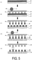
- FIGS. 5(A) to 5(E) are schematic diagrams illustrating an example of a transfer method by a microcontact printing method.
- the transfer method is a letterpress printing scheme using a mold. The description thereof will be given below with reference to FIGS. 5(A) to 5(E) .
- a metal complex composition 42 containing the above-described metal complex (hereinafter, also referred to as the metal complex composition 42) is evenly applied on a flat plate 41. It is preferable that the flat plate 41 have a smooth surface, and be unlikely to deform due to its high rigidity.
- a material of the flat plate 41 include glass; silicon; resin such as polycarbonate, polypropylene, polyethylene or the like; a metal; and a combination of these materials or the like.
- the metal complex composition 42 As an application method of the metal complex composition 42, a known or commonly used method may be used. For example, a spray method, a spin coating method, a screen printing method or the like may be used.
- the thickness of a coating film of the metal complex composition 42 is, for example, preferably in a range from 0.5 ⁇ m to 20 ⁇ m, more preferably in a range from 0.5 ⁇ m to 10 ⁇ m, and further more preferably in a range from 0.5 ⁇ m to 5 ⁇ m. In the case where the coating film thickness of the metal complex composition 42 is in the range form 0.5 ⁇ m to 5 ⁇ m, the metal complex composition 42 contains a suitable amount of metal complex, thereby making it possible to sufficiently join the semiconductor element 11 to the substrate 12 at the time of thermal fusion.
- the mold 30 is pressed against the metal complex composition 42 having been applied.
- the mold 30 is pressed in such a manner that the side at which a protrusion 44 is present faces the flat plate 41.
- a pressure is applied as needed from a side opposite to the side where the mold 30 is pressed against the metal complex composition 42 by a roller 43. It is preferable for the pressure to be 1000 Pa or larger, more preferable to be 10000 Pa or larger, and further more preferable to be 100000 Pa or larger.
- the mold 30 is evenly pressed against the flat plate 41 side without nonuniformity by the roller 43. Accordingly, the metal complex composition 42 can evenly adhere to the protrusion 44 of the mold 30.
- the mold 30 is separated from the flat plate 41.
- the metal complex composition 42 is separated from the flat plate 41 while being adsorbed on the protrusion 44 of the mold 30.
- the mold 30 is pressed against the substrate 12 having the electrode 15. It is preferable that the electrode 15 be disposed at a location facing the protrusion 44 when the substrate 12 faces the mold 30.
- the electrodes 15 may be disposed at the locations facing all of the protrusions 44, or at the locations facing some of the protrusions 44 as needed.
- the metal complex composition 42 adsorbed onto the protrusion 44 is pressed against the electrode 15 of the substrate 12.
- a pressure is applied as needed from a side opposite to the side where the mold 30 is pressed against the metal complex composition 42 by a roller 45. It is preferable for the pressure to be 1000 Pa or larger, more preferable to be 10000 Pa or larger, and further more preferable to be 100000 Pa or larger. With this, the mold 30 is evenly pressed against the substrate 12 side without nonuniformity by the roller 45. Accordingly, the metal complex composition 42 can evenly adhere onto the electrode 15 of the substrate 12.
- the mold 30 is separated from the substrate 12.
- the metal complex composition 42 is separated from the mold 30 while being adsorbed on the electrode 15 of the substrate 12.
- the microcontact printing method using the mold 30 may precisely transfer the metal complex composition 42 to a plurality of locations on the electrodes 15 at a time.
- the metal complex composition 42 may be transferred onto the terminal 14 on the semiconductor element 11 side instead of being transferred onto the electrode 15 on the substrate 12 side.
- the metal complex composition 42 may be transferred onto both the electrode 15 and the terminal 14. In the following description of the method for mounting the semiconductor element on the substrate, a case in which the metal complex composition 42 is transferred onto the terminal 14 on the semiconductor element 11 side will be explained.
- a transfer ratio indicating transfer properties of a transfer pattern obtained by the above transfer method, transfer precision, and positional deviation preferably satisfy the following criteria. Based on the observation results obtained by using an optical microscope, each transfer pattern is evaluated.
- the transfer ratio is preferably 98% or greater, more preferably 99% or greater, and most preferably 100%.
- the complex composition 42 may be precisely transferred onto a plurality of locations at a time on the electrodes 15.
- the transfer ratio is calculated by substituting the observation result into Formula (1) given below.
- Transfer ratio % number of dots having been successfully transferred per set of 10 ⁇ 10 dots at a central portion of the transfer pattern / 100 ⁇ 100
- the transfer precision is preferably 50% or greater, more preferably 80% or greater, and most preferably 100%.
- the metal complex composition 42 may be precisely transferred onto the plurality of locations at a time on the electrodes 15.
- the transfer precision is calculated by substituting the observation result into Formula (2) given below.
- Transfer precision % transfer pattern diameter / pillar diameter ⁇ 100
- the transfer pattern diameter is a size of one dot of the transfer pattern formed on a glass substrate.
- the pillar diameter is a pillar size of each mold used for the transfer.
- the size of the dot corresponds to d2 in FIG. 5(E)
- the pillar size of the mold corresponds to d1 in FIG. 5(E) .
- the positional deviation is preferably 10 ⁇ m or less, more preferably 6 ⁇ m or less, further more preferably 2 ⁇ m or less, and 0 ⁇ m. That is, a case of no positional deviation is most preferable.
- the metal complex composition 42 may be precisely transferred onto the plurality of locations at a time on the electrodes 15. The positional deviation is calculated by substituting the observation result into Formula (3) given below.
- Positional deviation the center point of the transfer pattern ⁇ the center point on the setting
- the center point of the transfer pattern is the center position of the transferred dot pattern.
- the center point on the setting is the center position of the dot pattern when the transfer is carried out precisely with no deviation.
- the positional deviation between the joining portion 13 and the electrode 15 or terminal 14 is preferably 10 ⁇ m or less, more preferably 6 ⁇ m or less, further more preferably 2 ⁇ m or less, and 0 ⁇ m. That is, a case of no positional deviation is most preferable.
- the positional deviation is calculated by substituting the observation result into Formula (4) given below.
- Positional deviation electrode or terminal center point ⁇ joining portion center point
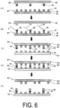
- FIGS. 6(A) to 6(E) are schematic diagrams illustrating a method for mounting a semiconductor element onto a substrate according to the present disclosure (hereinafter, also referred to simply as a mounting method).
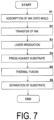
- FIG. 7 is a flowchart illustrating the mounting method of the present disclosure. The description thereof will be given below with reference to FIGS. 6(A) to 6(E) and FIG. 7 .
- an LED display is explained as an example of a mounted structure.
- the microcontact printing method is described with reference to a case of using the transfer method described above, but is not limited thereto. The same contents as those of the transfer method described above are omitted in the description of the mounting method.
- the LED display is a device in which the plurality of semiconductor elements 11 are mounted on the substrate 12, as illustrated in FIG. 1(A) , for example.
- the plurality of semiconductor elements 11 include three types of LED elements of R, G, and B. Therefore, it is necessary to mount each LED element at a position determined for each of the types of R, G and B on the substrate 12.
- the LED elements of three types of R, G, and B need to be mounted on the substrate 12 in an orderly manner with no deviation to prevent the generation of color unevenness or the like.
- the metal complex composition 42 is evenly adsorbed on the tip of the protrusion 44 of the mold 30.
- the metal complex composition 42 containing the metal complex is previously adsorbed onto the mold 30 according to the transfer method described above (S1 in FIG. 7 ).
- the LED chip board 61 is a member where a plurality of LED elements 62, which are semiconductor elements, are loaded on a chip board 63.
- the plurality of LED elements 62 are the LED elements of R among R, G, and B.
- the LED element 62 includes the terminal 14.
- the terminal 14 is disposed on the LED element 62 at a side in an opposite direction with respect to a side connected to the chip board 63.
- the protrusions 44 are preferably formed to overlap only the LED elements 62 at the locations where the LED elements of R are required. With this, when the mold 30 is pressed against the LED chip board 61, the protrusions 44 may be in contact with the locations where the LED elements of R are required. Thereafter, the mold 30 is separated from the LED chip board 61.
- the metal complex composition 42 adsorbed on the tip of the protrusion 44 is transferred onto the terminal 14 of the LED element 62 in contact with the metal complex composition 42 (S2 in FIG. 7 ).
- the mounting method may precisely transfer the metal complex composition 42 onto a plurality of locations at a time.
- the metal complex composition 42 transferred onto the terminal 14 is irradiated with a laser L (S3 in FIG. 7 ). It is sufficient that at least the metal complex composition 42 is irradiated with the laser L, and it is unnecessary for the entire chip board 63 to be irradiated with the laser. Further, it is preferable that all of the metal complex compositions 42 be evenly irradiated with the laser. This causes metal nanoparticles to be evenly deposited from the metal complex composition 42 on the terminal 14. A mass containing the metal nanoparticles deposited from the metal complex composition 42 is referred to as a metal nanoparticle group 47. That is, the metal complex composition 42 changes to the metal nanoparticle group 47 by laser irradiation. Heating (pre-baking) may be performed before laser irradiation as needed. The heating before laser irradiation may facilitate an increase of the deposition speed of the metal nanoparticles within the metal complex composition 42.
- the substrate 12 is prepared.
- the plurality of electrodes 15 are formed on the surface of the substrate 12.
- the electrodes 15 are preferably formed at the locations corresponding to at least the three types of LED elements of R, G, and B.
- the LED chip board 61 is pressed against the substrate 12 including the electrodes 15 (S4 in FIG. 7 ). With this, the plurality of LED elements 62 at the locations where the metal nanoparticle group 47 is formed are in contact with the electrodes 15 at the corresponding locations. At this time, the terminal 14 on the LED element 62 is brought into contact with the electrode 15 on the substrate 12 via the metal nanoparticle group 47. In other words, the terminal 14 and the electrode 15 are in contact with each other while pinching the metal nanoparticle group 47 containing the metal nanoparticles therebetween.
- Heating is performed while the terminal 14 and the electrode 15 are in contact with each other via the metal nanoparticle group 47 (S5 in FIG. 7 ).
- the metal nanoparticles within the metal nanoparticle group 47 are thermally fused by heating, thereby forming the joining portion 13.
- the joining portion 13 may be mixed with part of the terminal 14 and electrode 15 dissolved by the thermal fusion, and may be integrated with the terminal 14 and electrode 15. Thus, the terminal 14 and the electrode 15 are joined more firmly.
- the LED chip board 61 is separated from the substrate 12 (S6 in FIG. 7 ).
- the plurality of LED elements 62 which are the LED elements of R, are precisely mounted on the substrate 12 at a time.
- the LED elements of G or B may be mounted on the substrate 12.
- the LED elements of the three types of R, G, and B may be mounted on the substrate 12 at a time for each type. Accordingly, the time and manpower may be significantly reduced compared to a case in which the LED elements 62 are mounted one by one on the substrate 12.
- Production Example 1 a case in which the mold is a film formed of a cured product of a resin composition is exemplified.
- PDMS liquid polysiloxane
- CAT 260 available from Shin-Etsu Chemical Co., ltd.
- a master mold (made of silicon, a square with a side of 20 mm in a plan view, a transfer portion being a square with a side of 5 mm in the plan view, 100 x 100 holes, the hole size being 10 ⁇ m, the hole depth being 10 ⁇ m, the shortest distance between holes being 10 ⁇ m, the shortest distance from an edge for holes in the transfer portion being 20 ⁇ m) imparted with a pattern of recesses and protrusions and having a thickness of 1 mm in the lamination direction was fixed onto a glass substrate.
- a frame made of Teflon (trademark), the inner size being a square with a side of 20 mm in a plan view, the thickness in the lamination direction being 3 mm
- the prepared liquid polysiloxane composition 1 was fed into a space surrounded by the master mold and the frame.
- the fed liquid polysiloxane composition 1 was degassed under reduced pressure (pressure 10 kPa) for 30 minutes, and then a glass substrate was pasted on the upper portion of the liquid polysiloxane composition 1 while preventing bubbles from entering into a gap between the glass substrate and the liquid polysiloxane composition 1.
- a mold (A) After having cured the liquid polysiloxane composition 1 at 150°C for two hours, the aforementioned glass substrate, frame, and master mold were separated to obtain a mold (A).
- a film-shaped mold (A) with a film thickness of 2 mm was obtained, where a pillar-shaped pattern (size of a protrusion pattern: 10 ⁇ m, height of a protrusion: 10 ⁇ m) was formed on the surface of the mold.
- Production Example 2 a case where the mold is a fibrous core materialcontaining mold will be described.
- a cellulose nonwoven fabric (40 mm square) was prepared as the fibrous core material.
- the same description as that in Production Example 1 is omitted in the description of Production Example 2.
- PDMS liquid polysiloxane
- CAT 260 available from Shin-Etsu Chemical Co., ltd.
- acetone 10/1/3.
- a gadget in which a cellulose nonwoven fabric is set stretching over an aluminum-made frame having an opening of 30 mm square was put into the liquid polysiloxane composition 2 stored in a tray, and was left therein for 30 minutes to cause the cellulose nonwoven fabric to be impregnated with the liquid polysiloxane composition 2.
- the aluminum-made frame was pulled up and an excess of the liquid polysiloxane composition 2 was wiped off with a squeegee, the aluminum-made frame was left still for 24 hours at 23°C in a state of being vertically suspended. Thereafter, the liquid polysiloxane composition 2 was cured by heating at 150°C for two hours to fabricate a sheet-shaped mold base material (thickness in the lamination direction: 0.5 mm).
- a master mold was fixed on a glass substrate, and a frame (made of Teflon (trademark), the inner size being a square with a side of 20 mm in a plan view, the thickness in the lamination direction being 2.0 mm) was fixed onto the glass substrate to surround the master mold.
- the prepared liquid polysiloxane composition 1 was fed into a space surrounded by the master mold and the frame. After degassing under reduced pressure, the fabricated sheet-shaped mold base material was pasted on the upper portion of the liquid polysiloxane composition 1 while preventing bubbles from entering into a gap between the sheet-shaped mold base material and the liquid polysiloxane composition 1.
- a mold (B) the thickness in the lamination direction (a location where the sheet-shaped mold base material and the cured product of the liquid polysiloxane composition 1 were laminated: 1.5 mm).
- Production Example 3 a mold used in Reference Example 1 is described. The same description as that in Production Example 1 is omitted in the description of Production Example 3.
- Preparation Examples Transfer Examples 1 and 2, and Reference Example 1 are described below.
- the preparation of a copper complex composition is described.
- the mold (A) obtained in Production Example 1 was used in Transfer Example 1
- the mold (B) obtained in Production Example 2 was used in Transfer Example 2
- the mold (C) obtained in Production Example 3 was used in Reference Example 1.
- Glyoxylic acid copper (available from FUJIFILM Wako Pure Chemical Corporation) in an amount of 0.95 g was dissolved in a mixed solution of 1-ml 2-aminoethanol and 2-ml ethanol to prepare a glyoxylic acid copper solution of 1.7 mol/L.
- Formic acid copper tetrahydrate (available from FUJIFILM Wako Pure Chemical Corporation) in an amount of 1.15 g was dissolved in 3 ml of 40-wt.% methylamine methanol to prepare a methylamine copper complex solution of 1.7 mol/L.
- a copper complex composition A containing an ⁇ -keto acid copper complex and methylamine copper complex was prepared by mixing the prepared glyoxylic acid copper solution and methylamine copper complex solution.
- Glyoxylic acid copper (available from FUJIFILM Wako Pure Chemical Corporation) in an amount of 0.55 g was dissolved in a mixed solution of 1-ml 2-aminoethanol and 2-ml ethanol to prepare a glyoxylic acid copper solution of 1 mol/L.
- Formic acid copper tetrahydrate (available from FUJIFILM Wako Pure Chemical Corporation) in an amount of 0.65 g was dissolved in 3 ml of 40-wt.% methylamine methanol to prepare a methylamine copper complex solution of 1 mol/L.
- a copper complex composition B containing an ⁇ -keto acid copper complex and methylamine copper complex was prepared by mixing the prepared glyoxylic acid copper solution and methylamine copper complex solution.
- the prepared copper complex composition A in an amount of 0.1 ml was subjected to spin coating (3000 rpm, 30 seconds) onto slide glass to fabricate a liquid coating film with a film thickness of 0.1 ⁇ m. Subsequently, the mold (A) of Production Example 1 was pressed onto the fabricated liquid coating film. The copper complex composition A attached to a protrusion of the mold (A) was transferred onto a glass substrate. The copper complex composition A transferred onto the glass substrate was heated (pre-baked) for 10 minutes at 80°C.
- the transfer patterns (A) to (C) obtained in Transfer Examples 1 and 2 and Reference Example 1 were observed by using an optical microscope (DM4000M, available from Leica Microsystems). The transfer ratio, the transfer precision, and the positional deviation were evaluated based on the observation results of the optical microscope by the following methods.
- Transfer ratio % number of dots having been successfully transferred per set of 10 ⁇ 10 dots at a central portion of the transfer pattern/100 ⁇ 100
- the transfer properties in the transfer ratio (that is, indicating the percentage of successful transfers in 100 pillar patterns) were evaluated by the following evaluation criteria.
- Transfer precision % transfer pattern diameter/pillar diameter ⁇ 100
- the transfer pattern diameter a size of one dot of the transfer pattern formed on the glass substrate was measured.
- the pillar diameter is a pillar size of each mold used for the transfer.
- the transfer properties in the transfer precision were evaluated by the following evaluation criteria.
- the center point of the transfer pattern is the center position of the transferred dot pattern.
- the center point on the setting is the center position of the dot pattern when the transfer is carried out precisely with no deviation.
- the transfer properties in the positional deviation were evaluated by the following evaluation criteria.
- the transfer properties of the transfer patterns (A) and (B) obtained in Transfer Examples 1 and 2 were confirmed to be superior in any of the transfer ratio, transfer precision, and positional deviation to the transfer properties of the transfer pattern (C) obtained in Reference Example 1. From this, it was confirmed that the transfer was performed onto the glass substrate in accordance with the protrusion shape of the mold more faithfully in each of the molds produced using the PDMS of Production Examples 1 and 2 than in the mold produced using the cycloolefin copolymer of Production Example 3. It was also confirmed that the transfer properties of the transfer pattern (B) obtained in Transfer Example 2 were more excellent than the transfer properties of the transfer pattern (A) obtained in Transfer Example 1. From this, it was confirmed that mold (B) was reinforced with the cellulose nonwoven fabric and exhibited stable transfer properties without being affected by a tensile force during the transfer.
- the prepared copper complex composition B in an amount of 0.1 ml was subjected to spin coating (3000 rpm, 30 seconds) onto slide glass to fabricate a liquid coating film with a film thickness of 1.0 ⁇ m. Subsequently, the mold (B) of Production Example 2 was pressed onto the fabricated liquid coating film. The copper complex composition B attached to a protrusion of the mold (B) was transferred onto a smooth copper plate. The copper complex composition B transferred onto the copper plate was heated (pre-baked) for 10 minutes at 80°C.
- copper nanoparticles were deposited by CO 2 laser irradiation (distance between the laser and a composition layer: 145 mm, sweep rate: 20 mm/s, output: 8.0 W) to obtain a transfer pattern containing the copper nanoparticles formed on the copper plate.
- the copper plate was set on a glass substrate including a copper bump having the same pattern shape as that of the master mold.
- the copper bump on the glass substrate was laminated with an orientation facing the transfer pattern transferred on the copper plate.
- the laminated glass substrate and copper plate were heated at 200°C for 30 minutes.
- the copper nanoparticles in the transfer pattern were thermally fused with the copper bump on the glass substrate. This resulted in the copper plate being joined with the copper bump on the glass substrate.
- the joining state was observed from the glass surface by using an optical microscope (DM4000M, available from Leica Microsystems). From the observation result by the optical microscope, it was confirmed that the copper plate was joined with the copper bump on the glass substrate.
- Appendix 1 A mounted structure in which a semiconductor element including a terminal is mounted on a substrate including an electrode, the mounted structure including a joining portion in which the terminal and the electrode are joined opposing each other,
- Appendix 2 The mounted structure according to Appendix 1, wherein the metal complex includes a copper complex.
- Appendix 3 The mounted structure according to Appendix 2, wherein the copper complex includes a first copper complex formed of a keto acid and a copper ion, and a second copper complex formed of a copper ion and a ligand containing a nitrogen atom.
- Appendix 4 The mounted structure according to Appendix 3, wherein the sum of the contents of the first copper complex and the second copper complex is in a range from 90 wt.% to 5 wt.% (preferably from 80 wt.% to 10 wt.%) of the whole of a composition forming the metal complex.
- Appendix 5 The mounted structure according to Appendix 3 or 4, wherein the molar ratio of the first copper complex and the second copper complex (first copper complex: second copper complex) is in a range from 9:1 to 1:9 (preferably from 8:2 to 2:8).
- Appendix 6 The mounted structure according to any one of Appendices 2 to 5, wherein the molar concentration of copper with respect to the whole composition forming the metal complex is in a range from 0.5 M (mol/L) to 3.0 M (mol/L).
- Appendix 7 The mounted structure according to any one of Appendices 1 to 6, wherein the median size of the metal nanoparticles is in a range from 0.3 nm to 100 nm (preferably from 0.3 nm to 50 nm, more preferably from 0.3 nm to 10 nm).
- Appendix 8 The mounted structure according to any one of Appendices 1 to 7, wherein a mold used in the microcontact printing method contains polysiloxane as a constituent material.
- Appendix 9 The mounted structure according to any one of Appendices 1 to 8, wherein the mold used in the microcontact printing method uses a mold made of a film or a mold containing a fibrous core material (preferably a mold made of polysiloxane containing a fibrous core material), a linear expansion coefficient of the mold being 200 ppm/K or less (preferably 100 ppm/K or less, more preferably 50 ppm/K or less) and a size of the mold being unchanged before and after being used repeatedly using a solvent.
- a mold made of a film or a mold containing a fibrous core material preferably a mold made of polysiloxane containing a fibrous core material
- a linear expansion coefficient of the mold being 200 ppm/K or less (preferably 100 ppm/K or less, more preferably 50 ppm/K or less)
- a size of the mold being unchanged before and after being used repeatedly using a solvent.
- Appendix 10 The mounted structure according to Appendix 9, wherein the mold containing the fibrous core material is a mold in which a mold portion imparted with a pattern shape of a recess-protrusion shape is laminated on the fibrous core material solidified with resin (preferably with polysiloxane).
- Appendix 11 The mounted structure according to Appendix 10, wherein the fibrous core material solidified with the resin has a structure in which the fibrous core material is impregnated with the resin.
- Appendix 12 The mounted structure according to any one of Appendices 9 to 11, wherein the fibrous core material is nonwoven fabric.
- a positional deviation calculated by Formula (4) given below with respect to the electrode or the terminal and the joining portion is 10 ⁇ m or less (preferably 6 ⁇ m or less, more preferably 2 ⁇ m or less, and further more preferably 0 ⁇ m).
- Positional deviation electrode or terminal center point ⁇ joining portion center point
- Appendix 14 The mounted structure according to any one of Appendices 1 to 13, wherein the laser irradiation is performed using a CO 2 laser or an Er laser.
- Appendix 15 The mounted structure according to any one of Appendices 1 to 14, wherein the semiconductor element is an LED element in which a length of the longest line among the lines connecting any two points on an outer periphery of the semiconductor element in a plan view is 100 ⁇ m or less.
- Appendix 16 An LED display including the mounted structure according to any one of Appendices 1 to 15.
- a mounting method for mounting a semiconductor element including a terminal onto a substrate including an electrode that is a bump of a bulk metal material disposed on the substrate including:
- Appendix 18 The mounting method according to Appendix 17, wherein the metal complex includes a copper complex.
- Appendix 19 The mounting method according to Appendix 18, wherein the metal complex includes a first copper complex formed of a keto acid and a copper ion, and a second copper complex formed of a copper ion and a ligand containing a nitrogen atom.
- Appendix 20 The mounting method according to Appendix 19, wherein the sum of the contents of the first copper complex and the second copper complex is in a range from 90 wt.% to 5 wt.% (preferably from 80 wt.% to 10 wt.%) of the whole of a composition forming the metal complex.
- Appendix 21 The mounting method according to Appendix 19 or 20, wherein the molar ratio of the first copper complex and the second copper complex (first copper complex: second copper complex) is in a range from 9:1 to 1:9 (preferably from 8:2 to 2:8).
- Appendix 22 The mounting method according to any one of Appendices 18 to 21, wherein the molar concentration of copper with respect to the whole composition forming the metal complex is in a range from 0.5 M (mol/L) to 3.0 M (mol/L).
- Appendix 23 The mounting method according to any one of Appendices 17 to 22, wherein the median size of the metal nanoparticles is in a range from 0.3 nm to 100 nm (preferably from 0.3 nm to 50 nm, more preferably from 0.3 nm to 10 nm).
- Appendix 24 The mounting method according to any one of Appendices 17 to 23, wherein the microcontact printing method includes a step of causing a metal complex composition to be adsorbed onto a protrusion included in a mold.
- Appendix 25 The mounting method according to any one of Appendices 17 to 24, wherein the microcontact printing method includes a step of performing the laser irradiation on the metal complex composition adsorbed on the protrusion included in the mold.
- Appendix 26 The mounting method according to Appendix 25, wherein the metal complex composition is heated prior to the laser irradiation.
- Appendix 27 The mounting method according to any one of Appendices 17 to 26, wherein the mold used in the microcontact printing method contains polysiloxane as a constituent material.
- Appendix 28 The mounting method according to any one of Appendices 17 to 27, wherein the mold used in the microcontact printing method uses a mold made of a film or a mold containing a fibrous core material (preferably a mold made of polysiloxane containing a fibrous core material), a linear expansion coefficient of the mold being 200 ppm/K or less (preferably 100 ppm/K or less, more preferably 50 ppm/K or less) and a size of the mold being unchanged before and after being used repeatedly using a solvent.
- a mold made of a film or a mold containing a fibrous core material preferably a mold made of polysiloxane containing a fibrous core material
- a linear expansion coefficient of the mold being 200 ppm/K or less (preferably 100 ppm/K or less, more preferably 50 ppm/K or less)
- a size of the mold being unchanged before and after being used repeatedly using a solvent.
- Appendix 29 The mounting method according to Appendix 28, wherein the mold containing the fibrous core material is a mold in which a mold portion imparted with a pattern shape of a recess-protrusion shape is laminated on the fibrous core material solidified with resin (preferably with polysiloxane).
- Appendix 30 The mounting method according to Appendix 29, wherein the fibrous core material solidified with the resin has a structure in which the fibrous core material is impregnated with the resin.
- Appendix 31 The mounting method according to any one of Appendices 28 to 30, wherein the fibrous core material is nonwoven fabric.
- Appendix 32 The mounting method according to any one of Appendices 17 to 31, wherein the laser irradiation is performed using a CO 2 laser or an Er laser.
- Appendix 33 The mounting method according to any one of Appendices 17 to 32, wherein the semiconductor element is an LED element in which a length of the longest line among the lines connecting any two points on an outer periphery of the semiconductor element in a plan view is 100 ⁇ m or less.
- the transfer pattern diameter is a size of one dot of the transfer pattern formed on a glass substrate.
- the pillar diameter is a pillar size of each mold used for the transfer.
- the center point of the transfer pattern is the center position of the transferred dot pattern.
- the center point on the setting is the center position of the dot pattern when the transfer is carried out precisely with no deviation.
- the mounting method of the present disclosure may mount a plurality of semiconductor elements on a substrate at a time efficiently and precisely with little joining deviation.
- the mounted structure of the present disclosure is a structure in which the semiconductor elements are precisely mounted on the substrate at a time with little joining deviation.
- the mounting method and the mounted structure of the present disclosure may be preferably used, for example, as an optical component such as an LED (including an LED display), a display element for head-up display, a backlight of a liquid crystal display or the like, lighting, a visible light communication device or the like.
- the semiconductor elements 11 can be efficiently and precisely mounted on the substrate, and therefore the mounted structure of the present disclosure may be preferably used as a specially miniaturized device, for example, as a micro LED or the like.
Landscapes
- Engineering & Computer Science (AREA)
- Microelectronics & Electronic Packaging (AREA)
- Manufacturing & Machinery (AREA)
- Led Device Packages (AREA)
- Electric Connection Of Electric Components To Printed Circuits (AREA)
- Wire Bonding (AREA)
Abstract
Description
- The present disclosure relates to a mounted structure in which a semiconductor element is mounted on a substrate, an LED display including the mounted structure, and a mounting method for mounting the semiconductor element on the substrate. The present application claims priority to
JP 2020-150004 filed in Japan on September 7, 2020 - As a method for producing a printed circuit wiring board that is used in forming an electronic circuit by fixing electronic components onto a surface of the printed circuit wiring board and connecting the electronic components with wiring lines, a method (subtractive method) is known in which a material with a metal layer formed on the entire surface of an insulating substrate by a wet process (nonelectrolytic plating, electrolytic plating, or the like) or by a dry process (vacuum vapor deposition, sputtering, or the like) is used as a starting material, an unwanted portion of the metal layer of the starting material is etched utilizing a mask formed by using a photolithographic method, and metal wiring lines are formed by removing the mask after the completion of the etching. In recent years, the printed circuit wiring boards have been required to form finer wiring patterns to facilitate the densification of wiring boards accompanying the developments in miniaturization and functionality of electronic devices, but it is difficult for the subtractive method to precisely form a fine wiring pattern. The forming of a bump for connecting devices on the wiring lines and the joining the contact points with each other require significantly high precision, and therefore are carried out through complex processes.
- In particular, in display devices such as displays equipped with precision components such as micro LEDs, as miniaturization is carried on, higher resolution is required. For example, in a micro LED display (µ-LED), about 24.9 million micro LEDs (three types of R, G, B) need to be precisely disposed on one substrate at 4K resolution. When the micro LEDs are disposed one by one on the substrate, the process needs a long-term. Because of this, it is required to efficiently form the wiring pattern. To meet this requirement, an ink-jet scheme is known as a method for forming a finer wiring pattern on a substrate at once (Patent Document 1). In the ink-jet scheme of
Patent Document 1, a wiring pattern is formed on the substrate by discharging a metal nanoparticle paste through a nozzle onto the substrate and then heating. In addition, a contact printing scheme is also reported in which a paste containing conductive particles is applied on a surface of a resin template having been subjected to patterning including recesses and protrusions, and the surface of the resin template is pressed against a SiO2/Si substrate, thereby forming a pattern of the conductive material on the substrate (Patent Document 2). A production method is also reported in which a composition layer is formed by imparting a composition containing a copper complex to a substrate, and laser irradiation is performed on the composition layer to deposit copper, thereby producing a conductor on the substrate (Patent Document 3). -
- Patent Document 1:
JP 4539284 B - Patent Document 2:
JP 2007-110054 A - Patent Document 3:
WO 2018/212345 - The ink-jet scheme of
Patent Document 1 is a method of directly discharging a metal nanoparticle paste through a nozzle onto a substrate. At this time, the metal nanoparticle paste may scatter, blur, or spread on the substrate when observed at the nano-level. Due to this, there is a risk of a reduction in precision of the wiring pattern. In the contact printing scheme ofPatent Document 2, a silver nano-paste is applied on a resin template to form a layer of the silver nano-paste having ups and downs according to the recesses and protrusions on the template. Thereafter, the template is pressed against the substrate to transfer only the silver nano-paste applied to the protruding portions onto the SiO2/Si substrate. As a result, the silver nano-paste applied to the recessed portions of the template remains after the transfer, and therefore it is necessary to eliminate the remaining silver nano-paste by washing for successive use of the template. Accordingly, there is a risk that the same template cannot be used successively, thereby causing a reduction in production efficiency. In the production method for producing a conductor ofPatent Document 3, only the formation of the conductor on the substrate is carried out, and it is not disclosed that a semiconductor element can be mounted thereon with little joining deviation on the substrate. - Thus, an object of the present disclosure is to provide: a mounted structure which is excellent in precision with little joining deviation and can be produced efficiently, and in which a semiconductor element is mounted on a substrate; an LED display including the mounted structure; and a mounting method for mounting the semiconductor element on the substrate.
- Through extensive study to accomplish the object described above, the inventors of the present disclosure have found that it is possible to achieve a mounted structure that is excellent in precision with little joining deviation and can be produced efficiently by depositing metal nanoparticles, by laser irradiation, from a metal complex transferred onto an electrode which is a bump of a bulk metal material disposed on the substrate, by using a microcontact printing method. The present disclosure has been completed based on these findings.
- That is, the present disclosure provides a mounted structure in which a semiconductor element including a terminal is mounted on a substrate including an electrode. The mounted structure includes a joining portion in which the terminal and the electrode are joined opposing each other, the electrode is a bump of a bulk metal material disposed on the substrate, and the joining portion is produced by thermally fusing metal nanoparticles, the metal nanoparticles being deposited from a metal complex by laser irradiation, the metal complex having been transferred onto at least one of the electrode or the terminal by using a microcontact printing method.
- In addition, the present disclosure provides a mounting method for mounting a semiconductor element including a terminal onto a substrate including an electrode. The electrode is a bump of a bulk metal material disposed on the substrate. The mounting method includes transferring a metal complex onto at least one of the electrode or the terminal by using a microcontact printing method, depositing metal nanoparticles from the metal complex by laser irradiation, and performing thermal fusion in a state in which the terminal and the electrode are in contact with and oppose each other via the deposited metal nanoparticles.
- It is preferable that the above-described metal complex include a copper complex formed of a keto acid and a copper ion, and a copper complex formed of a copper ion and a ligand containing a nitrogen atom.
- A mold used in the microcontact printing method described above preferably contains polysiloxane as a constituent material.
- The mold used in the microcontact printing method preferably uses a mold made of a film or a mold made of polysiloxane including a fibrous core material, a linear expansion coefficient of the mold being 200 ppm/K or less and a size of the mold being unchanged before and after being used repeatedly using a solvent.
- It is preferable that the laser irradiation be performed using a CO2 laser or an Er laser.
- The semiconductor element is preferably an LED element in which the length of the longest line among the lines connecting any two points on the outer periphery of the semiconductor element in a plan view is 100 µm or less.
- The present disclosure provides an LED display including the mounted structure described above.
- According to the mounted structure or the mounting method of the present disclosure, it is possible to achieve the mounted structure that is excellent in precision with little joining deviation and can be produced efficiently. In addition, the mounted structure of the present disclosure may be suitably used as an LED display.
-
-
FIG. 1(A) is a perspective view in which part of a mounted structure of the present disclosure is enlarged and illustrated, andFIG. 1(B) is a partial cross-sectional view ofFIG. 1(A) . -
FIG. 2(A) is a plan view in which part of a mounted structure of the present disclosure is enlarged and illustrated, andFIG. 2(B) is a plan view in which part of a modified example of a mounted structure of the present disclosure is enlarged and illustrated. -
FIG. 3(A) is a plan view of a master mold,FIG. 3(B) is a partially enlarged plan view ofFIG. 3(A), and FIG. 3(C) is a partially enlarged plan view ofFIG. 3(B) . -
FIGS. 4(A) to 4(E) are schematic diagrams illustrating an example of a method for forming a mold. -
FIGS. 5(A) to 5(E) are schematic diagrams illustrating an example of transfer by a microcontact printing method. -
FIGS. 6(A) to 6(E) are schematic diagrams illustrating a mounting method of the present disclosure. -
FIG. 7 is a flowchart illustrating a mounting method of the present disclosure. - Hereinafter, embodiments for carrying out the present disclosure will be described. Note that each of the configurations, combinations thereof, and the like in each of the embodiments are an example, and various additions, omissions, substitutions, and other changes may be made as appropriate without departing from the spirit of the present disclosure. The present disclosure is not limited to the embodiments and is limited only to the claims.
-
FIG. 1(A) is a perspective view in which part of a mounted structure (hereinafter, also referred to simply as a mounted structure) 10 of the present disclosure is enlarged and illustrated, andFIG. 1(B) is a partial cross-sectional view ofFIG. 1(A) .FIG. 2(A) is a plan view in which part of the mountedstructure 10 is enlarged and illustrated, andFIG. 2(B) is a plan view in which part of a modified example of the mountedstructure 10 is enlarged and illustrated. InFIG. 1(A) , only asemiconductor element 11 and asubstrate 12 are illustrated, and the other members are omitted. As illustrated inFIG. 1(A), FIG. 1(B) , andFIG. 2(A) , the mountedstructure 10 includes a plurality ofsemiconductor elements 11, thesubstrate 12, and a plurality of joiningportions 13. Thesemiconductor element 11 includes aterminal 14, and thesubstrate 12 includes anelectrode 15. Thesemiconductor element 11 is mounted on thesubstrate 12 in such a manner that theterminal 14 and theelectrode 15 oppose each other. The joiningportion 13 joins the terminal 14 and theelectrode 15. That is, the plurality ofsemiconductor elements 11 are each mounted on thesubstrate 12 with the joiningportion 13 interposed therebetween. - The
semiconductor element 11 is an electronic component using a semiconductor, and particularly indicates a microscale element herein. Thesemiconductor elements 11 include asemiconductor element 111, asemiconductor element 112, and asemiconductor element 113. For example, thesemiconductor element 111 is a red micro LED, thesemiconductor element 112 is a green micro LED, and thesemiconductor element 113 is a blue micro LED. One pixel is constituted of onesemiconductor element 111, onesemiconductor element 112, and onesemiconductor element 113. A plurality of the pixels each constituted of thesemiconductor element 111,semiconductor element 112, andsemiconductor element 113 are disposed being aligned at predetermined intervals on thesubstrate 12. In the present embodiment, three types of micro LEDs are given as examples of thesemiconductor elements 11, but in accordance with the specifications, all the micro LEDs may be the same type, or a plurality of micro LEDs other than the above three types may be included. The size, the shape, the number of elements, and the like may be different depending on the luminance or the like of the individual semiconductor elements. For example, one pixel may be constituted by a combination of foursemiconductor elements 11 including onesemiconductor element 111, onesemiconductor element 112, and twosemiconductor elements 113. - The length of the longest line among the lines connecting any two points on the outer periphery of the
semiconductor element 11 in a plan view is preferably 100 µm or less. In the following, the plan view indicates a view when seen from a direction perpendicular to a planar direction of thesubstrate 12 or the like. To be specific, the semiconductor element 11 (111, 112, 113) is formed in a rectangular shape having a diagonal line of 100 µm or less in length in a plan view, for example. When thesemiconductor element 11 has a rectangular shape in a plan view, the length of the diagonal line is more preferably 70 µm or less, and further more preferably 35 µm or less. -
FIG. 2(B) illustrates a mountedstructure 101, which is a modified example of the mountedstructure 10. In the description of the mountedstructure 101, description similar to that of the mountedstructure 10 is omitted, and only different portions are described. As illustrated inFIG. 2(B) , the semiconductor element 11 (111, 112, 113) is formed in a circular shape having a diameter of 100 µm or less. When thesemiconductor element 11 has a circular shape in a plan view, the diameter thereof is more preferably 50 µm or less, and further more preferably 20 µm or less. The shape of thesemiconductor element 11 is not limited to a rectangular shape or a circular shape, and other shapes such as a polygonal shape, an elliptical shape and the like may be employed in accordance with the specifications. - The
substrate 12 is a planar substrate including theelectrode 15. Examples of the planar substrate include a glass plate; a semiconductor such as silicon, gallium arsenide, gallium nitride or the like; a composite substrate obtained by a base material such as glass cloth, nonwoven fabric or the like being impregnated with resin such as an epoxy resin and being cured: a resin substrate of an epoxy resin cured product, an engineering plastic such as a liquid crystal polymer, polycarbonate, polypropylene, polyethylene or the like; a metal substrate; and a combination of these materials. Thesubstrate 12 may include, in addition to theelectrode 15, a pattern structure such as a fine wiring line, a crystalline structure, an optical waveguide, an optical structure such as holography or the like, as needed. - The
substrate 12 is preferably formed in a rectangular shape having a diagonal line of 600 mm or less in length in a plan view, for example. When thesemiconductor element 11 has a rectangular shape in a plan view, the length of the diagonal line is more preferably 100 mm or less, and further more preferably 75 mm or less. The shape of thesubstrate 12 is not limited to a rectangular shape, and other shapes such as a polygonal shape, a circular shape, an elliptical shape and the like may be employed in accordance with the specifications. - The
electrode 15 is a bump (protrusion) of a bulk metal material disposed on thesubstrate 12. It is preferable that the bulk metal material be electrically conductive and have low resistance. Examples of components constituting the bulk metal material include metal, metal salts such as metal oxide, carbon and the like. The components constituting the bulk metal material may be composed of only one type of component, or may include a plurality of types of components. Among the above-mentioned components, metal is preferred as the component constituting the bulk metal material. The metal may be, for example, a single element such as gold, silver, palladium, platinum, nickel, copper, iron, lead, lithium, cobalt, manganese, aluminum, zinc, bismuth, silicon, tin, cadmium, indium or the like, a plurality of elements of these metals, or metal oxides or salts of these metals. - The
electrode 15 is disposed on thesubstrate 12 in accordance with the specifications of the mountedstructure 10. Theelectrode 15 is disposed at a position corresponding to each of thesemiconductor elements 11, for example. - The joining
portion 13 includes a material having electrical conductivity. Examples of the material having electrical conductivity include metal, metal salts such as metal oxide, and a mixture of these materials. Among these, the metal is preferably used for thermally fusing the terminal 14 and theelectrode 15. Examples of the metal include gold, silver, palladium, platinum, nickel, copper, iron, lead, lithium, cobalt, manganese, aluminum, zinc, bismuth, silicon, tin, cadmium, indium and the like. Among the metals, a metal unlikely to be oxidized is preferred. Copper is particularly preferred among the metals. Copper is inexpensive and is unlikely to be oxidized when it is in the form of a nano-size particle, and therefore copper may be easily handled in the atmosphere. This makes it possible to easily join the terminal 14 and theelectrode 15 in the atmosphere. - The joining
portion 13 is formed, for example, by thermally fusing the metal nanoparticles made of the metal described above. Regarding the heating conditions of the thermal fusion, the temperature is preferably in a range from 100°C to 200°C, more preferably in a range from 100°C to 150°C, and further more preferably in a range from 100°C to 120°C. When the temperature is 100°C or higher, the metal nanoparticles may be sufficiently fused and integrated. The heating time is preferably 120 minutes or less, more preferably 15 minutes or less, and further more preferably 5 minutes or less. This makes it possible to sufficiently join the terminal 14 and theelectrode 15. The joiningportion 13 may be mixed and integrated with part of the terminal 14 and theelectrode 15, which are fused by the thermal fusion. With this, the terminal 14 may be more firmly joined to theelectrode 15. - Metal nanoparticles are deposited by laser irradiation from a metal complex contained in a metal complex composition. The metal complex composition is a composition transferred onto the
electrode 15 by using the microcontact printing method. The metal complex composition may be transferred onto the terminal 14 on thesemiconductor element 11 side instead of being transferred onto theelectrode 15 on thesubstrate 12 side. The metal complex composition may be transferred onto both theelectrode 15 and the terminal 14. In other words, it is sufficient that the metal complex composition is transferred onto at least one of theelectrode 15 or the terminal 14. - The microcontact printing method may transfer the metal complex composition containing the metal complex to a plurality of locations at a time by using a mold described below. When metal nanoparticles formed of the metal complex are used for forming the joining
portion 13, the usage amount of metal may be reduced compared to the case of using a bulk metal, and the metal may be disposed in a fine region by using the microcontact printing method. The transfer by the microcontact printing method will be described in detail later. - A method of depositing metal nanoparticles from the metal complex contained in the metal complex composition by using laser irradiation treatment will be described below. Although copper is taken as an example of the metal herein, any metal can be used as long as metal nanoparticles can be deposited therefrom in a similar manner.
- It is preferable that a copper complex composition be a composition including a first copper complex formed of a keto acid and a copper ion, and a second copper complex formed of a copper ion and a ligand containing a nitrogen atom, for example.
- The first copper complex is preferably formed of a keto acid and a copper ion (keto acid copper). Examples of the first copper complex include α-keto acid copper, β-keto acid copper and γ-keto acid copper, such as glyoxylic acid copper. The first copper complex may be one type among these materials, or a combination of two or more types thereof. The second copper complex is preferably formed of a copper ion and a ligand containing a nitrogen atom. Examples of the second copper complex include monoalkylamine copper complexes (CnH2n+1NH2Cu: n is an integer) such as a methylamine copper complex, an ethylamine copper complex and the like, and amine-based copper complexes such as a dialkylamine copper complex, a trialkylamine copper complex, an ethylene diamine copper complex, an ethanolamine copper complex and the like. The second copper complex may be one type among these materials, or a combination of two or more types thereof.
- The content ratio of the first copper complex and the second copper complex contained in the copper complex composition is not particularly limited, but is preferably in a range from 90 wt.% to 5 wt.% of the whole composition, and more preferably in a range from 80 wt.% to 10 wt.%, for example. The molar ratio of the first copper complex and the second copper complex contained in the copper complex composition (first copper complex: second copper complex) is not particularly limited, but is preferably in a range from 9:1 to 1:9, and more preferably in a range from 8:2 to 2:8. The molar concentration of copper with respect to the whole copper complex composition (the sum of copper contained in the first copper complex and copper contained in the second copper complex) is not particularly limited, but is preferably in a range from 0.5 M (mol/L) to 3.0 M (mol/L), for example.
- The metal complex composition may further include a solvent that may dissolve the metal complex contained in the metal complex composition. Examples of such a solvent include alcohol-based solvents such as methanol, ethanol, aminoethanol and the like, ketone-based solvents such as cyclohexanone, amide-based solvents such as dimethyl formamide, terpene-based solvents such as terpineol, esterbased solvents and the like. The solvent may be one type among the solvents described above, or a combination of two or more types thereof. The metal complex composition may contain additives other than the metal complex and the medium as necessary. Examples of the additives include a viscosity regulator, a pH regulator and the like.
- A laser used for laser irradiation is not particularly limited as long as it causes the decomposition of the metal complex contained in the metal complex composition and the deposition of metal. From the perspective of achieving favorable deposition of metal nanoparticles in the atmosphere, the laser is preferably an infrared laser or near infrared laser, and more preferably an CO2 laser or an Er laser. Laser irradiation may be performed evenly on all of the metal complex compositions, or may be performed in a patterned form as necessary. There may be included a step of removing a composition layer other than a portion thereof where the metal nanoparticles are deposited by laser irradiation. For example, an unwanted metal complex composition may be removed by using a solvent capable of dissolving the metal complex contained in the metal complex composition.
- From the metal complex composition transferred onto the
electrode 15, the metal is deposited by laser irradiation. Specifically, an irradiated portion is instantaneously heated by laser irradiation; due to this heat, the ligand of the metal complex is decomposed into CO2, CO and H2O, and removed from the metal complex composition in the form of gas. The decomposition of the ligand causes the metal ions forming the metal complex to be reduced, and the metal nanoparticles are deposited. As a result, metal nanoparticles with high purity having high metal concentration are obtained. - A plurality of the metal nanoparticles produced by deposition are melted and grown together in a laser irradiation region. A reaction in which the metal nanoparticles are deposited from the metal complex progresses in a very short time. That is, significantly small size metal nanoparticles are deposited before the metal complex reacts with oxygen in the atmosphere. Accordingly, it is assumed that the metal nanoparticles can be formed favorably from the metal complex composition because of being unlikely to be affected by oxidation even in the atmosphere. The deposited metal nanoparticles are melted at a temperature lower than the melting point of the metal, and therefore the metal nanoparticles may be deposited with low energy. Since the metal complex composition is in a state in which the metal complex is dissolved, problems such as aggregation, oxidation and the like are unlikely to occur and preservation stability is excellent compared to a material using metal particles.
- The average particle size (median size, D50) of the metal nanoparticles deposited is not particularly limited, but is preferably in a range from 0.3 nm to 100 nm, more preferably in a range from 0.3 nm to 50 nm, and further more preferably in a range from 0.3 nm to 10 nm. When the average particle size of the metal nanoparticles is in a range from 0.5 nm to 100 nm, problems such as aggregation, oxidation and the like are unlikely to occur, and the joining
portion 13 formed evenly with high purity is obtained after thermal fusion. The average particle size of the metal nanoparticles is a value determined by the number average; for example, particle sizes of 100 metal nanoparticles optionally selected from an image captured using a transmission electron microscope are measured, and then the average particle size of the metal nanoparticles can be determined from the average value of the measured particle sizes. - As described above, the copper complex composition is preferably a composition including the first copper complex and the second copper complex. The second copper complex has a lower decomposition temperature than the first copper complex and is more easily decomposed than the first copper complex. Thus, it is assumed that the deposition of copper from the second copper complex occurs earlier to form a nucleus, then the growth of copper nanoparticles based on the nucleus is promoted by the copper deposited from the first copper complex. The copper nanoparticles formed from the copper complex composition have surface smoothness superior to that of the copper nanoparticles formed using a composition including only the first copper complex. Because of this, the copper nanoparticles deposited from the copper complex composition may be formed more densely on the
electrode 15. - The metal nanoparticles deposited on the
electrode 15 are thermally fused. With this, the joiningportion 13 is formed. The joiningportion 13 joins the terminal 14 and theelectrode 15. Thus, thesemiconductor element 11 is mounted on thesubstrate 12. Since the plurality of joiningportions 13 are formed at a time using the microcontact printing method, thesemiconductor elements 11 may be efficiently and precisely mounted on thesubstrate 12. - The mounted
structure 10 of the present disclosure may be preferably used, for example, as an optical component such as an LED (including an LED display), a display element for head-up display, a backlight of a liquid crystal display or the like, lighting, a visible light communication device or the like. Thesemiconductor elements 11 can be efficiently and precisely mounted on thesubstrate 12, and therefore the mountedstructure 10 may be preferably used as a micro LED, which is a specially miniaturized device, or the like. Examples of the micro LED include a device in which the length of the longest line among the lines connecting any two points on the outer periphery of the LED element in a plan view (for example, the length of the diameter in a case of a circular shape) is 100 µm or less. A mold used in the microcontact printing method and a master mold for forming the mold are described below. -
FIG. 3(A) is a plan view of amaster mold 20,FIG. 3(B) is a plan view in which atransfer portion 21, which is part ofFIG. 3(A) , is enlarged and illustrated, andFIG. 3(C) is a plan view in which part of thetransfer portion 21 ofFIG. 3(B) is further enlarged and illustrated. Themaster mold 20 is a mold for forming the mold to be used in the microcontact printing method. A pattern shape of an inverted recess-protrusion shape for imparting a desired shape to the mold is imparted to themaster mold 20; the pattern shape of the inverted recess-protrusion shape (an inverted shape of the desired mold) corresponds to the desired shape of the mold. Themaster mold 20 is a structure in which fine shapes of recesses and protrusions are formed on a surface of Si, quartz, metal or the like, and this structure is very expensive and is also referred to as a master. A mold is formed based on the expensive master mold and the pattern formation is carried out by the microcontact printing method using the aboveformed mold, and thus the costs may be reduced significantly. - As illustrated in
FIG. 3(A) , themaster mold 20 includes thetransfer portion 21 and aperipheral portion 22. The outer shape of each of thetransfer portion 21 and theperipheral portion 22 is rectangular in a plan view, and theperipheral portion 22 surrounds thetransfer portion 21. The length of one side of the master mold 20 (the length of one side of the perimeter of the peripheral portion 22) is preferably in a range from 10 mm to 700 mm, more preferably in a range from 10 mm to 150 mm, and further more preferably in a range from 10 mm to 100 mm. The length of one side of thetransfer portion 21 is preferably in a range from 10 mm to 600 mm, more preferably in a range from 10 mm to 100 mm, and further more preferably in a range from 10 mm to 50 mm. The shape of each of thetransfer portion 21 and theperipheral portion 22 is not limited to a rectangular shape, and other shapes such as a polygonal shape, a circular shape, an elliptical shape and the like may be employed in accordance with the specifications. - As illustrated in
FIGS. 3(B) and 3(C) , thetransfer portion 21 has a recess-protrusion shape on the surface thereof. Thetransfer portion 21 includes a plurality ofrecesses 23 formed being separated from each other by a predetermined interval, for example. Therecess 23 has a shape recessed in a columnar shape from the surface of thetransfer portion 21 to the interior thereof, for example. The shape of therecess 23 is not limited to a columnar shape, and a polygonal prism shape or the like may be employed in accordance with the specifications. The side of therecess 23 recessed to the interior may be formed in a planar shape, or may be formed in a three-dimensional shape, for example, in a hemispherical shape. - When the
recess 23 is formed in a columnar shape, a diameter (L1) of therecess 23 in a plan view is preferably 100 µm or less, more preferably 50 µm or less, and further more preferably 10 µm or less. The depth of therecess 23 is preferably 200 µm or less, more preferably 100 µm or less, and further more preferably 20 µm or less. - An interval (L2) between the
recesses 23 of thetransfer portion 21 is designed in accordance with the layout of each color of the semiconductor elements 11 (111, 112, 113). The interval between therecesses 23 of thetransfer portion 21 may be changed as appropriate in accordance with the specifications of the mountedstructure 10. For example, when themaster mold 20 and thesubstrate 12 are overlapped each other, therecesses 23 are formed at positions overlapping all of theelectrodes 15 on thesubstrate 12 or at positions overlapping at least some of theelectrodes 15. Here, in the case where the metal complex composition is transferred onto the terminal 14 on thesemiconductor element 11 side, when themaster mold 20 and thesemiconductor elements 11 are overlapped each other, therecesses 23 are formed at positions overlapping all of theterminals 14 on thesemiconductor elements 11 or at positions overlapping at least some of theterminals 14. Since the plurality ofsemiconductor elements 11 are present, it is preferable to treat them in such a manner that the plurality ofsemiconductor elements 11 are loaded on a chip board, for example. - A shortest distance (L3) of the
recess 23 from anedge 24 of thetransfer portion 21 is preferably 100 µm or less, preferably 30 µm or less, and more preferably 10 µm or less. - The mold of the present disclosure (hereinafter, also referred to simply as the mold) is made of a cured product or a solidified product of a resin composition (hereinafter, also referred to as a mold-forming resin composition) that forms a mold. The mold is, for example, a film made of a cured product or a solidified product of a resin composition that forms a mold. The mold may be a structure in which a cured product or a solidified product of the mold-forming resin composition is laminated on a base member. A mold containing a fibrous core material may be cited as an example. The base member includes the fibrous core material, and supports a cured product or a solidified product of the mold-forming resin composition.
- The cured product or the solidified product of the mold-forming resin composition has a recess-protrusion shape on the surface thereof. The
master mold 20 imparts, to the mold, a pattern shape of an inverted recess-protrusion shape corresponding to the shape of themaster mold 20. At a location in the mold corresponding to thetransfer portion 21 of themaster mold 20, a plurality of the protrusions are formed at the locations corresponding to the plurality ofrecesses 23. The mold-forming resin composition includes resin and a curable composition for forming a mold. - It is preferable that the mold use a mold including a film or a fibrous core material, a linear expansion coefficient of the mold being 200 ppm/K or less and a size of the mold being unchanged before and after being used repeatedly using a solvent. The linear expansion coefficient of the mold is more preferably 100 ppm/K or less, and further more preferably 50 ppm/K or less. When the linear expansion coefficient of the mold is 200 ppm/K or less, a change in volume due to heat of the mold is small. As a result, deformation of the mold due to heat or the like generated by friction is suppressed, and more precise transfer may be carried out when used in the microcontact printing method. When the size of the mold does not change before and after the mold being used repeatedly using a solvent, a change in volume of the mold caused by the solvent is small. Therefore, the deformation of the mold due to the solvent contained in ink is suppressed, and thus more precise transfer may be carried out when the mold is used in the microcontact printing method. The value of the change in size before and after the mold being used repeatedly using a solvent is obtained by comparing the dimensions of the initial mold with the dimensions of the mold after being used repeatedly using the solvent. As the dimensions of the mold after being used repeatedly using the solvent, for example, the dimensions of a mold that is impregnated with the solvent for one hour at room temperature and then is subjected to drying under reduced pressure (10 Pa, 80°C, two hours) may be tentatively used.
- Examples of the mold including the fibrous core material include a mold in which there is laminated a mold part where a pattern shape of a recess-protrusion shape is imparted onto the fibrous core material hardened with resin similar to the mold. Examples of the fibrous core material include fabric including a material having low elasticity. Specific examples thereof include nonwoven fabric made of cellulose, cotton or the like, and woven fabric such as glass cloth. By using a mold including a fibrous core material, the mold is strengthened by the fibrous core material, and stable transfer properties may be obtained without being affected by a tensile force at the time of transfer. Furthermore, since the fibrous core material suppresses the volume change due to heat and the swelling due to the solvent, the deformation of the mold itself may be suppressed.
- Examples of the resin for forming the above-discussed mold include polysiloxane (dimethylpolysiloxane or the like) as a silicone-based resin, a fluorine-based resin, polyolefin-based resin (polyethylene, polypropylene, polycyclic olefin, or the like), polyethersulfone-based resin, polycarbonate-based resin, polyester-based resin (polyarylate, polyethylene terephthalate, polyethylene naphthalate, or the like), polyamide-based resin, polymethyl methacrylate and the like.
- Among the above resins, polysiloxane is particularly preferred. In the curing of the mold-forming resin composition, for example, a three-dimensional crosslinking reaction by hydrosilylation to an unsaturated double bond, a radical polymerization, an epoxy reaction, or the like may be used. Examples of the curable composition include such as polysiloxane containing an epoxy compound and the like. When polysiloxane is used as the resin, the compatibility with a curable composition such as an epoxy compound is excellent, and the contact angle is likely to be small. In addition, when polysiloxane is used as the above-discussed resin and curable composition, the obtained mold is excellent in flexibility, and thus a protruding portion of the mold may extend flexibly along other contacting objects such as a flat plate and may be in contact with the contacting objects when used in the microcontact printing method. As a result, the ink applied to the flat plate and the like may be adsorbed onto the protruding portion of the mold without nonuniformity. Since the mold is excellent in releasability and flexibility, the mold may be more easily taken out from the
master mold 20. - In addition to the above-described components, other components such as a release agent may be added to the mold-forming resin composition as needed. For example, an organic solvent may be added to adjust the viscosity. Examples of the organic solvent include a saturated or unsaturated hydrocarbon solvent such as pentane, hexane, heptane, octane, petroleum ether or the like; an aromatic hydrocarbon-based solvent such as benzene, toluene, xylene or the like; ketone such as acetone, methyl ethyl ketone, methyl isobutyl ketone, methyl n-amyl ketone, cyclohexanone or the like; alcohol such as methanol, ethanol, n-butanol or the like; and ether such as 1,2-dimethoxyethane, tetrahydrofuran, dioxane or the like. One of these can be used alone or two or more in combination. It is preferable that the viscosity of the mold-forming resin composition (at 25°C) be adjusted to be approximately in a range from 1 to 100 mPa·s, for example, from the perspective of application properties. The viscosity of the mold-forming resin composition may be measured using a digital viscometer (model No. "DVU-EII", available from TOKIMEC INC.) under the conditions of rotor: standard 1°34' x R24, temperature: 25°C, and rotation speed: from 0.5 to 10 rpm. An example of a method for forming a mold is described below.
-
FIGS. 4(A) to 4(E) are schematic diagrams illustrating an example of a method for forming a mold.FIG. 4(A) is a schematic plan view, andFIG. 4(B) is a schematic cross-sectional view ofFIG. 4(A) . First, as illustrated inFIG. 4(A) and FIG. 4(B) , a mold set in which themaster mold 20 is set is prepared. Specifically, themaster mold 20 and aframe 32 are disposed on aplate 31. In this case, themaster mold 20, theplate 31, and theframe 32 each have a square shape in a plan view, but the square shape is an example and the shape thereof is not limited to the square shape. - The
frame 32 is formed in a shape surrounding themaster mold 20 in a plan view. The length of each side on the inner side of theframe 32 is the same as the length of each side of themaster mold 20. In other words, in a case where themaster mold 20 is a square with a side of 20 mm in a plan view, the length of each side on the inner side of theframe 32 is 20 mm. With this, the periphery in a horizontal direction of themaster mold 20 is fitted into theframe 32. It is preferable for the thickness in the horizontal direction of theframe 32 in a plan view to be 0.5 mm or greater, preferable to be 1 mm or greater, and more preferable to be 10 mm or greater. The thickness in a vertical direction of theframe 32 is preferably a length obtained by adding a desired mold thickness to the thickness in a vertical direction of themaster mold 20. As a result, by filling the inner side of theframe 32 with a mold-formingresin composition 34 up to the edge on the upper side thereof, the mold having the desired thickness is obtained. Theplate 31 is preferably formed in a flat plate shape, and is provided with a plane direction being level. This makes it possible to obtain the mold in which unwanted nonuniformity in thickness in the horizontal direction is suppressed. - The material of the
plate 31 is preferably excellent in heat resistance, and examples thereof include an inorganic material such as glass, silicon or the like; resin such as a cycloolefin-based polymer, polycarbonate, polypropylene, polyethylene, epoxy or the like; metal; and a combination of these materials or the like. When theplate 31 has superior heat resistance, deformation thereof is suppressed when the mold is cured by heat, and the mold in which the recesses and protrusions are precisely transferred from themaster mold 20 is obtained. The material of theframe 32 preferably has heat resistance and chemical resistance, and examples thereof include fluorine resins such as Teflon (trademark), cycloolefin-based polymers and the like. When theframe 32 has heat resistance, deformation of theframe 32 is suppressed when the mold is cured by heat. When theframe 32 has chemical resistance, deformation of theframe 32 caused by the resin forming the mold is suppressed. Thus, the mold on which the recesses and protrusions of themaster mold 20 are precisely transferred is obtained. The surface of theframe 32 may be subjected to mold release processing with a fluorine-based silane coupling agent or the like as necessary. - Subsequently, as illustrated in
FIG. 4(C) , the mold-formingresin composition 34 described above is fed into a space surrounded by theframe 32 on themaster mold 20 of the mold set. The mold-formingresin composition 34 is filled in the space surrounded by themaster mold 20 and theframe 32. - Further, the mold-forming
resin composition 34 having been filled is preferably defoamed by a defoaming process. The defoaming may be carried out by a known or commonly used defoaming method. In particular, defoaming by decompression (decompression degassing, vacuum degassing) is preferred. The decompression degassing may be carried out, for example, by statically setting the mold set filled with the mold-formingresin composition 34 under a pressure of 0.1 kPa to 20 kPa for 1 to 10 minutes. As a result, bubbles within the mold-formingresin composition 34 are discharged to the outside. Thus, the bubbles adsorbed on the recesses and protrusions of themaster mold 20, for example, may be eliminated, and the mold on which the recesses and protrusions of themaster mold 20 are precisely transferred may be obtained. - Subsequently, as necessary, a
base member 35 is overlaid to be in close contact to the mold-formingresin composition 34 having been filled, as illustrated inFIG. 4(D) . The mold-formingresin composition 34 is sandwiched between themaster mold 20 and thebase member 35, and thebase member 35 may be a mold including the fibrous core material described above. The mold-formingresin composition 34 is likely to be integrated with thebase member 35 including the fibrous core material when being cured. After thebase member 35 is overlaid on the mold-formingresin composition 34, the laminated members, that is, theplate 31, themaster mold 20, the mold-formingresin composition 34, and thebase member 35 may be pressed in a lamination direction. Consequently, the adhesion of each member is increased, and a variation in thickness in the lamination direction may be prevented. The pressure during pressing is, for example, from 0.01 to 100 MPa. - Subsequently, the mold-forming
resin composition 34 laminated with theplate 31, themaster mold 20, and thebase member 35 is cured through a curing process. In the curing process, the mold-formingresin composition 34 may be cured by conducting a polymerization reaction of a curable compound (particularly, a cationcurable compound) contained in the mold-formingresin composition 34. The curing method may be appropriately selected from known or commonly used methods. The curing method is not particularly limited, and examples thereof include a method of heating and/or a method of irradiation with active energy rays. - Heating is preferred as the curing method. In the case of heating, it is unnecessary to transmit light for irradiation to the mold-forming
resin composition 34, and thus other members surrounding the mold-formingresin composition 34 are not required to have light-transmissive properties. As for the heating conditions, the temperature of heating is preferably 80°C or higher, more preferably 100°C or higher, and further more preferably 150°C or higher. When the temperature is 80°C or higher, the mold-formingresin composition 34 is sufficiently cured. The curing time is preferably 15 minutes or longer, more preferably 30 minutes or longer, and further more preferably 90 minutes or longer. When the curing time is 15 minutes or longer, the mold-formingresin composition 34 is sufficiently cured. The mold-formingresin composition 34 is integrated with thebase member 35 when being cured. As a result, themold 30, in which the mold-formingresin composition 34 and thebase member 35 are integrated, is formed. - In a case where curing is carried out by the method of irradiation with active energy rays, any of infrared rays, visible rays, ultraviolet rays, X-rays, electron beams, α-rays, β-rays, γ-rays and the like, for example, may be used as the active energy rays. Among these, ultraviolet rays are preferred in terms of excellent handling. A highpressure mercury lamp, ultra-high pressure mercury lamp, carbon arc lamp, xenon lamp, metal halide lamp or the like is used as the light source when irradiation with ultraviolet light is performed. The irradiation time depends on the type of the light source, the distance between the light source and the coated surface, and other conditions, but is several tens of seconds at the longest. The illuminance is, for example, approximately 5 to 200 mW/cm2. After the irradiation with the active energy ray, heating (post curing) may be performed as necessary to promote the curing.
- After the curing process, the
mold 30 having been formed may be taken out by being removed from theplate 31, theframe 32, and themaster mold 20, as illustrated inFIG. 4(E) . Thus, themold 30 is obtained. - When the mold is a film formed of a cured product of the mold-forming
resin composition 34, a member similar to theplate 31 is used in place of thebase member 35 in the above-discussed mold forming method. After the mold-formingresin composition 34 is cured, the cured mold-formingresin composition 34 may be taken out by being removed from theplate 31, theframe 32, themaster mold 20, and the member similar to theplate 31. With this, the mold that is a film formed of a cured product of the mold-formingresin composition 34 is obtained. -
FIGS. 5(A) to 5(E) are schematic diagrams illustrating an example of a transfer method by a microcontact printing method. The transfer method is a letterpress printing scheme using a mold. The description thereof will be given below with reference toFIGS. 5(A) to 5(E) . - First, as illustrated in
FIG. 5(A) , ametal complex composition 42 containing the above-described metal complex (hereinafter, also referred to as the metal complex composition 42) is evenly applied on aflat plate 41. It is preferable that theflat plate 41 have a smooth surface, and be unlikely to deform due to its high rigidity. Examples of a material of theflat plate 41 include glass; silicon; resin such as polycarbonate, polypropylene, polyethylene or the like; a metal; and a combination of these materials or the like. - As an application method of the
metal complex composition 42, a known or commonly used method may be used. For example, a spray method, a spin coating method, a screen printing method or the like may be used. The thickness of a coating film of themetal complex composition 42 is, for example, preferably in a range from 0.5 µm to 20 µm, more preferably in a range from 0.5 µm to 10 µm, and further more preferably in a range from 0.5 µm to 5 µm. In the case where the coating film thickness of themetal complex composition 42 is in the range form 0.5 µm to 5 µm, themetal complex composition 42 contains a suitable amount of metal complex, thereby making it possible to sufficiently join thesemiconductor element 11 to thesubstrate 12 at the time of thermal fusion. - Subsequently, as illustrated in
FIG. 5(B) , themold 30 is pressed against themetal complex composition 42 having been applied. Themold 30 is pressed in such a manner that the side at which aprotrusion 44 is present faces theflat plate 41. A pressure is applied as needed from a side opposite to the side where themold 30 is pressed against themetal complex composition 42 by aroller 43. It is preferable for the pressure to be 1000 Pa or larger, more preferable to be 10000 Pa or larger, and further more preferable to be 100000 Pa or larger. With this, themold 30 is evenly pressed against theflat plate 41 side without nonuniformity by theroller 43. Accordingly, themetal complex composition 42 can evenly adhere to theprotrusion 44 of themold 30. - As illustrated in
FIG. 5(C) , themold 30 is separated from theflat plate 41. At this time, themetal complex composition 42 is separated from theflat plate 41 while being adsorbed on theprotrusion 44 of themold 30. - As illustrated in
FIG. 5(D) , themold 30 is pressed against thesubstrate 12 having theelectrode 15. It is preferable that theelectrode 15 be disposed at a location facing theprotrusion 44 when thesubstrate 12 faces themold 30. Theelectrodes 15 may be disposed at the locations facing all of theprotrusions 44, or at the locations facing some of theprotrusions 44 as needed. - A side at which the
protrusion 44 of themold 30 is provided and a side at which theelectrode 15 of thesubstrate 12 is provided face each other and are pressed against each other. Thus, themetal complex composition 42 adsorbed onto theprotrusion 44 is pressed against theelectrode 15 of thesubstrate 12. A pressure is applied as needed from a side opposite to the side where themold 30 is pressed against themetal complex composition 42 by aroller 45. It is preferable for the pressure to be 1000 Pa or larger, more preferable to be 10000 Pa or larger, and further more preferable to be 100000 Pa or larger. With this, themold 30 is evenly pressed against thesubstrate 12 side without nonuniformity by theroller 45. Accordingly, themetal complex composition 42 can evenly adhere onto theelectrode 15 of thesubstrate 12. - As illustrated in
FIG. 5(E) , themold 30 is separated from thesubstrate 12. At this time, themetal complex composition 42 is separated from themold 30 while being adsorbed on theelectrode 15 of thesubstrate 12. Thus, the microcontact printing method using themold 30 may precisely transfer themetal complex composition 42 to a plurality of locations on theelectrodes 15 at a time. Themetal complex composition 42 may be transferred onto the terminal 14 on thesemiconductor element 11 side instead of being transferred onto theelectrode 15 on thesubstrate 12 side. Themetal complex composition 42 may be transferred onto both theelectrode 15 and the terminal 14. In the following description of the method for mounting the semiconductor element on the substrate, a case in which themetal complex composition 42 is transferred onto the terminal 14 on thesemiconductor element 11 side will be explained. - A transfer ratio indicating transfer properties of a transfer pattern obtained by the above transfer method, transfer precision, and positional deviation preferably satisfy the following criteria. Based on the observation results obtained by using an optical microscope, each transfer pattern is evaluated.
- The transfer ratio is preferably 98% or greater, more preferably 99% or greater, and most preferably 100%. When the transfer ratio is 98% or greater, the
complex composition 42 may be precisely transferred onto a plurality of locations at a time on theelectrodes 15. The transfer ratio is calculated by substituting the observation result into Formula (1) given below.
- The transfer precision is preferably 50% or greater, more preferably 80% or greater, and most preferably 100%. When the transfer precision is 50% or greater, the
metal complex composition 42 may be precisely transferred onto the plurality of locations at a time on theelectrodes 15. The transfer precision is calculated by substituting the observation result into Formula (2) given below.
- The transfer pattern diameter is a size of one dot of the transfer pattern formed on a glass substrate. The pillar diameter is a pillar size of each mold used for the transfer. For example, the size of the dot corresponds to d2 in
FIG. 5(E) , and the pillar size of the mold corresponds to d1 inFIG. 5(E) . - The positional deviation is preferably 10 µm or less, more preferably 6 µm or less, further more preferably 2 µm or less, and 0 µm. That is, a case of no positional deviation is most preferable. When the positional deviation is 10 µm or less, the
metal complex composition 42 may be precisely transferred onto the plurality of locations at a time on theelectrodes 15. The positional deviation is calculated by substituting the observation result into Formula (3) given below.
- The center point of the transfer pattern is the center position of the transferred dot pattern. The center point on the setting is the center position of the dot pattern when the transfer is carried out precisely with no deviation.
- That is, in the mounted structure of the present disclosure, the positional deviation between the joining
portion 13 and theelectrode 15 orterminal 14 is preferably 10 µm or less, more preferably 6 µm or less, further more preferably 2 µm or less, and 0 µm. That is, a case of no positional deviation is most preferable. The positional deviation is calculated by substituting the observation result into Formula (4) given below.
-
FIGS. 6(A) to 6(E) are schematic diagrams illustrating a method for mounting a semiconductor element onto a substrate according to the present disclosure (hereinafter, also referred to simply as a mounting method).FIG. 7 is a flowchart illustrating the mounting method of the present disclosure. The description thereof will be given below with reference toFIGS. 6(A) to 6(E) andFIG. 7 . In the description of the method for mounting a semiconductor element onto a substrate, an LED display is explained as an example of a mounted structure. Here, the microcontact printing method is described with reference to a case of using the transfer method described above, but is not limited thereto. The same contents as those of the transfer method described above are omitted in the description of the mounting method. - The LED display is a device in which the plurality of
semiconductor elements 11 are mounted on thesubstrate 12, as illustrated inFIG. 1(A) , for example. In the LED display, the plurality ofsemiconductor elements 11 include three types of LED elements of R, G, and B. Therefore, it is necessary to mount each LED element at a position determined for each of the types of R, G and B on thesubstrate 12. The LED elements of three types of R, G, and B need to be mounted on thesubstrate 12 in an orderly manner with no deviation to prevent the generation of color unevenness or the like. - First, as illustrated in
FIG. 6(A) , themold 30 and anLED chip board 61 are prepared. Themetal complex composition 42 is evenly adsorbed on the tip of theprotrusion 44 of themold 30. Themetal complex composition 42 containing the metal complex is previously adsorbed onto themold 30 according to the transfer method described above (S1 inFIG. 7 ). TheLED chip board 61 is a member where a plurality ofLED elements 62, which are semiconductor elements, are loaded on achip board 63. For example, the plurality ofLED elements 62 are the LED elements of R among R, G, and B. TheLED element 62 includes the terminal 14. The terminal 14 is disposed on theLED element 62 at a side in an opposite direction with respect to a side connected to thechip board 63. - The
protrusion 44 of themold 30, when overlaid on themold 30, overlaps some of the plurality ofLED elements 62 of theLED chip board 61 in a plan view. In a case where three types of LED elements are required as in the LED display, theprotrusions 44 are preferably formed to overlap only theLED elements 62 at the locations where the LED elements of R are required. With this, when themold 30 is pressed against theLED chip board 61, theprotrusions 44 may be in contact with the locations where the LED elements of R are required. Thereafter, themold 30 is separated from theLED chip board 61. - As illustrated in
FIG. 6(B) , themetal complex composition 42 adsorbed on the tip of theprotrusion 44 is transferred onto theterminal 14 of theLED element 62 in contact with the metal complex composition 42 (S2 inFIG. 7 ). In this manner, the mounting method may precisely transfer themetal complex composition 42 onto a plurality of locations at a time. - Subsequently, the
metal complex composition 42 transferred onto the terminal 14 is irradiated with a laser L (S3 inFIG. 7 ). It is sufficient that at least themetal complex composition 42 is irradiated with the laser L, and it is unnecessary for theentire chip board 63 to be irradiated with the laser. Further, it is preferable that all of themetal complex compositions 42 be evenly irradiated with the laser. This causes metal nanoparticles to be evenly deposited from themetal complex composition 42 on the terminal 14. A mass containing the metal nanoparticles deposited from themetal complex composition 42 is referred to as ametal nanoparticle group 47. That is, themetal complex composition 42 changes to themetal nanoparticle group 47 by laser irradiation. Heating (pre-baking) may be performed before laser irradiation as needed. The heating before laser irradiation may facilitate an increase of the deposition speed of the metal nanoparticles within themetal complex composition 42. - Subsequently, as illustrated in
FIG. 6(C) , thesubstrate 12 is prepared. As described above, the plurality ofelectrodes 15 are formed on the surface of thesubstrate 12. Theelectrodes 15 are preferably formed at the locations corresponding to at least the three types of LED elements of R, G, and B. - As illustrated in
FIG. 6(D) , theLED chip board 61 is pressed against thesubstrate 12 including the electrodes 15 (S4 inFIG. 7 ). With this, the plurality ofLED elements 62 at the locations where themetal nanoparticle group 47 is formed are in contact with theelectrodes 15 at the corresponding locations. At this time, the terminal 14 on theLED element 62 is brought into contact with theelectrode 15 on thesubstrate 12 via themetal nanoparticle group 47. In other words, the terminal 14 and theelectrode 15 are in contact with each other while pinching themetal nanoparticle group 47 containing the metal nanoparticles therebetween. - Heating is performed while the terminal 14 and the
electrode 15 are in contact with each other via the metal nanoparticle group 47 (S5 inFIG. 7 ). The metal nanoparticles within themetal nanoparticle group 47 are thermally fused by heating, thereby forming the joiningportion 13. As described above, the joiningportion 13 may be mixed with part of the terminal 14 andelectrode 15 dissolved by the thermal fusion, and may be integrated with the terminal 14 andelectrode 15. Thus, the terminal 14 and theelectrode 15 are joined more firmly. - Subsequently, as illustrated in
FIG. 6(E) , theLED chip board 61 is separated from the substrate 12 (S6 inFIG. 7 ). With this, the plurality ofLED elements 62, which are the LED elements of R, are precisely mounted on thesubstrate 12 at a time. By using a similar method, the LED elements of G or B may be mounted on thesubstrate 12. Thus, in the LED display, the LED elements of the three types of R, G, and B may be mounted on thesubstrate 12 at a time for each type. Accordingly, the time and manpower may be significantly reduced compared to a case in which theLED elements 62 are mounted one by one on thesubstrate 12. - Hereinafter, the present disclosure will be described more specifically with reference to examples, but the present disclosure is not limited to these examples, and modifications and improvements within the scope of achieving the object of the present disclosure are encompassed by the present disclosure. Molds used in Example 1, Transfer Examples 1 to 3, and Reference Example 1 were prepared by the methods described in Production Examples 1 to 3 given below.
- In Production Example 1, a case in which the mold is a film formed of a cured product of a resin composition is exemplified.
-
Liquid polysiloxane composition 1 was prepared by mixing a liquid polysiloxane (PDMS) ("SIM-260" available from Shin-Etsu Chemical Co., ltd.) and a curing agent ("CAT 260" available from Shin-Etsu Chemical Co., ltd.) in a ratio (weight ratio) of liquid polysiloxane/curing agent = 10/1. A master mold (made of silicon, a square with a side of 20 mm in a plan view, a transfer portion being a square with a side of 5 mm in the plan view, 100 x 100 holes, the hole size being 10 µm, the hole depth being 10 µm, the shortest distance between holes being 10 µm, the shortest distance from an edge for holes in the transfer portion being 20 µm) imparted with a pattern of recesses and protrusions and having a thickness of 1 mm in the lamination direction was fixed onto a glass substrate. - Subsequently, a frame (made of Teflon (trademark), the inner size being a square with a side of 20 mm in a plan view, the thickness in the lamination direction being 3 mm) was fixed onto the glass substrate to surround the master mold. The prepared
liquid polysiloxane composition 1 was fed into a space surrounded by the master mold and the frame. The fedliquid polysiloxane composition 1 was degassed under reduced pressure (pressure 10 kPa) for 30 minutes, and then a glass substrate was pasted on the upper portion of theliquid polysiloxane composition 1 while preventing bubbles from entering into a gap between the glass substrate and theliquid polysiloxane composition 1. After having cured theliquid polysiloxane composition 1 at 150°C for two hours, the aforementioned glass substrate, frame, and master mold were separated to obtain a mold (A). A film-shaped mold (A) with a film thickness of 2 mm was obtained, where a pillar-shaped pattern (size of a protrusion pattern: 10 µm, height of a protrusion: 10 µm) was formed on the surface of the mold. - In Production Example 2, a case where the mold is a fibrous core materialcontaining mold will be described. A cellulose nonwoven fabric (40 mm square) was prepared as the fibrous core material. The same description as that in Production Example 1 is omitted in the description of Production Example 2.
-
Liquid polysiloxane composition 2 was prepared by mixing a liquid polysiloxane (PDMS) ("SIM-260" available from Shin-Etsu Chemical Co., ltd.), a curing agent ("CAT 260" available from Shin-Etsu Chemical Co., ltd.), and acetone in a ratio (weight ratio) of liquid polysiloxane/curing agent/acetone = 10/1/3. A gadget in which a cellulose nonwoven fabric is set stretching over an aluminum-made frame having an opening of 30 mm square was put into theliquid polysiloxane composition 2 stored in a tray, and was left therein for 30 minutes to cause the cellulose nonwoven fabric to be impregnated with theliquid polysiloxane composition 2. After the aluminum-made frame was pulled up and an excess of theliquid polysiloxane composition 2 was wiped off with a squeegee, the aluminum-made frame was left still for 24 hours at 23°C in a state of being vertically suspended. Thereafter, theliquid polysiloxane composition 2 was cured by heating at 150°C for two hours to fabricate a sheet-shaped mold base material (thickness in the lamination direction: 0.5 mm). - Similar to Production Example 1, a master mold was fixed on a glass substrate, and a frame (made of Teflon (trademark), the inner size being a square with a side of 20 mm in a plan view, the thickness in the lamination direction being 2.0 mm) was fixed onto the glass substrate to surround the master mold. The prepared
liquid polysiloxane composition 1 was fed into a space surrounded by the master mold and the frame. After degassing under reduced pressure, the fabricated sheet-shaped mold base material was pasted on the upper portion of theliquid polysiloxane composition 1 while preventing bubbles from entering into a gap between the sheet-shaped mold base material and theliquid polysiloxane composition 1. After having cured theliquid polysiloxane composition 1, the glass substrate, the frame, and the master mold were separated to obtain a mold (B) (the thickness in the lamination direction (a location where the sheet-shaped mold base material and the cured product of theliquid polysiloxane composition 1 were laminated): 1.5 mm). - In Production Example 3, a mold used in Reference Example 1 is described. The same description as that in Production Example 1 is omitted in the description of Production Example 3.
- An amount of 10 g of cycloolefin copolymer TOPAS (available from Polyplastics Co., Ltd.) was dissolved in 100 ml of a toluene solvent. The prepared toluene solution was spin-coated on a quartz substrate, and then was subjected to heating for 10 minutes on a 100°C hot plate to remove the solvent. Thus, a coating film with a thickness of 2 to 10 µm was formed in a dry state. Subsequently, the above-discussed master mold was subjected to pressure transfer at 160°C using an imprint device (NM-0401, available from MEISYO KIKO Co., Ltd.). A mold (C) was obtained by mold releasing from the master mold at room temperature.
- Preparation Examples, Transfer Examples 1 and 2, and Reference Example 1 are described below. In Preparation Examples, the preparation of a copper complex composition is described. The mold (A) obtained in Production Example 1 was used in Transfer Example 1, the mold (B) obtained in Production Example 2 was used in Transfer Example 2, and the mold (C) obtained in Production Example 3 was used in Reference Example 1.
- Glyoxylic acid copper (available from FUJIFILM Wako Pure Chemical Corporation) in an amount of 0.95 g was dissolved in a mixed solution of 1-ml 2-aminoethanol and 2-ml ethanol to prepare a glyoxylic acid copper solution of 1.7 mol/L. Formic acid copper tetrahydrate (available from FUJIFILM Wako Pure Chemical Corporation) in an amount of 1.15 g was dissolved in 3 ml of 40-wt.% methylamine methanol to prepare a methylamine copper complex solution of 1.7 mol/L. A copper complex composition A containing an α-keto acid copper complex and methylamine copper complex was prepared by mixing the prepared glyoxylic acid copper solution and methylamine copper complex solution.
- Glyoxylic acid copper (available from FUJIFILM Wako Pure Chemical Corporation) in an amount of 0.55 g was dissolved in a mixed solution of 1-ml 2-aminoethanol and 2-ml ethanol to prepare a glyoxylic acid copper solution of 1 mol/L. Formic acid copper tetrahydrate (available from FUJIFILM Wako Pure Chemical Corporation) in an amount of 0.65 g was dissolved in 3 ml of 40-wt.% methylamine methanol to prepare a methylamine copper complex solution of 1 mol/L. A copper complex composition B containing an α-keto acid copper complex and methylamine copper complex was prepared by mixing the prepared glyoxylic acid copper solution and methylamine copper complex solution.
- The prepared copper complex composition A in an amount of 0.1 ml was subjected to spin coating (3000 rpm, 30 seconds) onto slide glass to fabricate a liquid coating film with a film thickness of 0.1 µm. Subsequently, the mold (A) of Production Example 1 was pressed onto the fabricated liquid coating film. The copper complex composition A attached to a protrusion of the mold (A) was transferred onto a glass substrate. The copper complex composition A transferred onto the glass substrate was heated (pre-baked) for 10 minutes at 80°C. Subsequently, copper nanoparticles were deposited by CO2 laser irradiation (distance between the laser and a composition layer: 145 mm, sweep rate: 20 mm/s, output: 8.0 W) to obtain a transfer pattern (A) containing the copper nanoparticles formed on the glass substrate.
- By the same operation as that in Transfer Example 1 except that the mold (B) of Production Example 2 was used, the copper complex composition A was transferred and the copper nanoparticles were deposited, thereby obtaining a transfer pattern (B) containing the copper nanoparticles formed on a glass substrate.
- By the same operation as that in Transfer Example 1 except that the mold (C) of Production Example 3 was used, the copper complex composition A was transferred and the copper nanoparticles were deposited, thereby obtaining a transfer pattern (C) containing the copper nanoparticles formed on a glass substrate.
- The transfer patterns (A) to (C) obtained in Transfer Examples 1 and 2 and Reference Example 1 were observed by using an optical microscope (DM4000M, available from Leica Microsystems). The transfer ratio, the transfer precision, and the positional deviation were evaluated based on the observation results of the optical microscope by the following methods.
- Each transfer ratio of the obtained transfer pattern was calculated by substituting the observation result into Formula (1) given below.

- The transfer properties in the transfer ratio (that is, indicating the percentage of successful transfers in 100 pillar patterns) were evaluated by the following evaluation criteria.
- Good: 98% ≤ transfer ratio: (good transfer properties)
- Poor: transfer ratio < 98%: (poor transfer properties)
- Each transfer precision of the obtained transfer pattern was calculated by substituting the observation result into Formula (2) given below.

- As the transfer pattern diameter, a size of one dot of the transfer pattern formed on the glass substrate was measured. The pillar diameter is a pillar size of each mold used for the transfer.
- The transfer properties in the transfer precision were evaluated by the following evaluation criteria.
- Excellent: 80% ≤ transfer precision < 105% (excellent transfer properties)
- Good: 50% ≤ transfer precision < 80% (good transfer properties)
- Poor: transfer precision < 50% (poor transfer properties)
- Each positional deviation of the obtained transfer pattern was calculated by substituting the observation result into Formula (3) given below.

- The center point of the transfer pattern is the center position of the transferred dot pattern. The center point on the setting is the center position of the dot pattern when the transfer is carried out precisely with no deviation.
- The transfer properties in the positional deviation were evaluated by the following evaluation criteria.
- Excellent: positional deviation ≤ 2 µm (Excellent transfer properties)
- Good: 2 µm < positional deviation ≤ 10 µm (good transfer properties)
- Poor: 10 µm < positional deviation (poor transfer properties)
- The above-described results are summarized in Table 1 given below.
-
Table 1 Transfer Example 1 Transfer Example 2 Reference Example 1 Mold (A) Good - - (B) - Good - (C) - - Good Evaluation of transfer properties Transfer ratio Good Good Poor Transfer precision Excellent Excellent Good Positional deviation Good Excellent Good - The transfer properties of the transfer patterns (A) and (B) obtained in Transfer Examples 1 and 2 were confirmed to be superior in any of the transfer ratio, transfer precision, and positional deviation to the transfer properties of the transfer pattern (C) obtained in Reference Example 1. From this, it was confirmed that the transfer was performed onto the glass substrate in accordance with the protrusion shape of the mold more faithfully in each of the molds produced using the PDMS of Production Examples 1 and 2 than in the mold produced using the cycloolefin copolymer of Production Example 3. It was also confirmed that the transfer properties of the transfer pattern (B) obtained in Transfer Example 2 were more excellent than the transfer properties of the transfer pattern (A) obtained in Transfer Example 1. From this, it was confirmed that mold (B) was reinforced with the cellulose nonwoven fabric and exhibited stable transfer properties without being affected by a tensile force during the transfer.
- The prepared copper complex composition B in an amount of 0.1 ml was subjected to spin coating (3000 rpm, 30 seconds) onto slide glass to fabricate a liquid coating film with a film thickness of 1.0 µm. Subsequently, the mold (B) of Production Example 2 was pressed onto the fabricated liquid coating film. The copper complex composition B attached to a protrusion of the mold (B) was transferred onto a smooth copper plate. The copper complex composition B transferred onto the copper plate was heated (pre-baked) for 10 minutes at 80°C. Subsequently, copper nanoparticles were deposited by CO2 laser irradiation (distance between the laser and a composition layer: 145 mm, sweep rate: 20 mm/s, output: 8.0 W) to obtain a transfer pattern containing the copper nanoparticles formed on the copper plate.
- Subsequently, the copper plate was set on a glass substrate including a copper bump having the same pattern shape as that of the master mold. At this time, the copper bump on the glass substrate was laminated with an orientation facing the transfer pattern transferred on the copper plate. The laminated glass substrate and copper plate were heated at 200°C for 30 minutes. The copper nanoparticles in the transfer pattern were thermally fused with the copper bump on the glass substrate. This resulted in the copper plate being joined with the copper bump on the glass substrate. The joining state was observed from the glass surface by using an optical microscope (DM4000M, available from Leica Microsystems). From the observation result by the optical microscope, it was confirmed that the copper plate was joined with the copper bump on the glass substrate.
- Each of the aspects disclosed herein may be combined with any other feature disclosed herein.
- Hereinafter, variations of the invention according to the present disclosure will be described.
- [Appendix 1] A mounted structure in which a semiconductor element including a terminal is mounted on a substrate including an electrode, the mounted structure including a joining portion in which the terminal and the electrode are joined opposing each other,
- wherein the electrode is a bump of a bulk metal material disposed on the substrate, and
- the joining portion is produced by thermally fusing metal nanoparticles, the metal nanoparticles being deposited from a metal complex by laser irradiation, the metal complex having been transferred onto at least one of the electrode or the terminal by using a microcontact printing method.
- [Appendix 2] The mounted structure according to
Appendix 1, wherein the metal complex includes a copper complex. - [Appendix 3] The mounted structure according to
Appendix 2, wherein the copper complex includes a first copper complex formed of a keto acid and a copper ion, and a second copper complex formed of a copper ion and a ligand containing a nitrogen atom. - [Appendix 4] The mounted structure according to
Appendix 3, wherein the sum of the contents of the first copper complex and the second copper complex is in a range from 90 wt.% to 5 wt.% (preferably from 80 wt.% to 10 wt.%) of the whole of a composition forming the metal complex. - [Appendix 5] The mounted structure according to
Appendix - [Appendix 6] The mounted structure according to any one of
Appendices 2 to 5, wherein the molar concentration of copper with respect to the whole composition forming the metal complex is in a range from 0.5 M (mol/L) to 3.0 M (mol/L). - [Appendix 7] The mounted structure according to any one of
Appendices 1 to 6, wherein the median size of the metal nanoparticles is in a range from 0.3 nm to 100 nm (preferably from 0.3 nm to 50 nm, more preferably from 0.3 nm to 10 nm). - [Appendix 8] The mounted structure according to any one of
Appendices 1 to 7, wherein a mold used in the microcontact printing method contains polysiloxane as a constituent material. - [Appendix 9] The mounted structure according to any one of
Appendices 1 to 8, wherein the mold used in the microcontact printing method uses a mold made of a film or a mold containing a fibrous core material (preferably a mold made of polysiloxane containing a fibrous core material), a linear expansion coefficient of the mold being 200 ppm/K or less (preferably 100 ppm/K or less, more preferably 50 ppm/K or less) and a size of the mold being unchanged before and after being used repeatedly using a solvent. - [Appendix 10] The mounted structure according to Appendix 9, wherein the mold containing the fibrous core material is a mold in which a mold portion imparted with a pattern shape of a recess-protrusion shape is laminated on the fibrous core material solidified with resin (preferably with polysiloxane).
- [Appendix 11] The mounted structure according to
Appendix 10, wherein the fibrous core material solidified with the resin has a structure in which the fibrous core material is impregnated with the resin. - [Appendix 12] The mounted structure according to any one of Appendices 9 to 11, wherein the fibrous core material is nonwoven fabric.
- The mounted structure according to any one of
Appendices 1 to 12, wherein a positional deviation calculated by Formula (4) given below with respect to the electrode or the terminal and the joining portion is 10 µm or less (preferably 6 µm or less, more preferably 2 µm or less, and further more preferably 0 µm).
- [Appendix 14] The mounted structure according to any one of
Appendices 1 to 13, wherein the laser irradiation is performed using a CO2 laser or an Er laser. - [Appendix 15] The mounted structure according to any one of
Appendices 1 to 14, wherein the semiconductor element is an LED element in which a length of the longest line among the lines connecting any two points on an outer periphery of the semiconductor element in a plan view is 100 µm or less. - [Appendix 16] An LED display including the mounted structure according to any one of
Appendices 1 to 15. - A mounting method for mounting a semiconductor element including a terminal onto a substrate including an electrode that is a bump of a bulk metal material disposed on the substrate, the mounting method including:
- transferring a metal complex onto at least one of the electrode or the terminal by using a microcontact printing method,
- depositing metal nanoparticles from the metal complex by laser irradiation, and
- performing thermal fusion in a state in which the terminal and the electrode are in contact with and oppose each other via the deposited metal nanoparticles.
- [Appendix 18] The mounting method according to Appendix 17, wherein the metal complex includes a copper complex.
- [Appendix 19] The mounting method according to Appendix 18, wherein the metal complex includes a first copper complex formed of a keto acid and a copper ion, and a second copper complex formed of a copper ion and a ligand containing a nitrogen atom.
- [Appendix 20] The mounting method according to Appendix 19, wherein the sum of the contents of the first copper complex and the second copper complex is in a range from 90 wt.% to 5 wt.% (preferably from 80 wt.% to 10 wt.%) of the whole of a composition forming the metal complex.
- [Appendix 21] The mounting method according to
Appendix 19 or 20, wherein the molar ratio of the first copper complex and the second copper complex (first copper complex: second copper complex) is in a range from 9:1 to 1:9 (preferably from 8:2 to 2:8). - [Appendix 22] The mounting method according to any one of Appendices 18 to 21, wherein the molar concentration of copper with respect to the whole composition forming the metal complex is in a range from 0.5 M (mol/L) to 3.0 M (mol/L).
- [Appendix 23] The mounting method according to any one of Appendices 17 to 22, wherein the median size of the metal nanoparticles is in a range from 0.3 nm to 100 nm (preferably from 0.3 nm to 50 nm, more preferably from 0.3 nm to 10 nm).
- [Appendix 24] The mounting method according to any one of Appendices 17 to 23, wherein the microcontact printing method includes a step of causing a metal complex composition to be adsorbed onto a protrusion included in a mold.
- [Appendix 25] The mounting method according to any one of Appendices 17 to 24, wherein the microcontact printing method includes a step of performing the laser irradiation on the metal complex composition adsorbed on the protrusion included in the mold.
- [Appendix 26] The mounting method according to Appendix 25, wherein the metal complex composition is heated prior to the laser irradiation.
- [Appendix 27] The mounting method according to any one of Appendices 17 to 26, wherein the mold used in the microcontact printing method contains polysiloxane as a constituent material.
- [Appendix 28] The mounting method according to any one of Appendices 17 to 27, wherein the mold used in the microcontact printing method uses a mold made of a film or a mold containing a fibrous core material (preferably a mold made of polysiloxane containing a fibrous core material), a linear expansion coefficient of the mold being 200 ppm/K or less (preferably 100 ppm/K or less, more preferably 50 ppm/K or less) and a size of the mold being unchanged before and after being used repeatedly using a solvent.
- [Appendix 29] The mounting method according to Appendix 28, wherein the mold containing the fibrous core material is a mold in which a mold portion imparted with a pattern shape of a recess-protrusion shape is laminated on the fibrous core material solidified with resin (preferably with polysiloxane).
- [Appendix 30] The mounting method according to Appendix 29, wherein the fibrous core material solidified with the resin has a structure in which the fibrous core material is impregnated with the resin.
- [Appendix 31] The mounting method according to any one of Appendices 28 to 30, wherein the fibrous core material is nonwoven fabric.
- [Appendix 32] The mounting method according to any one of Appendices 17 to 31, wherein the laser irradiation is performed using a CO2 laser or an Er laser.
- [Appendix 33] The mounting method according to any one of Appendices 17 to 32, wherein the semiconductor element is an LED element in which a length of the longest line among the lines connecting any two points on an outer periphery of the semiconductor element in a plan view is 100 µm or less.
- [Appendix 34] The mounting method according to any one of Appendices 17 to 33, wherein the transfer ratio calculated from Formula (1) given below when the metal complex is transferred onto at least one of the electrode or the terminal is 98% or greater (preferably 99% or greater, more preferably 100%).

- [Appendix 35] The mounting method according to any one of Appendices 17 to 34, wherein the transfer precision calculated from Formula (2) given below when the metal complex is transferred onto at least one of the electrode or the terminal is 50% or greater (preferably 80% or greater, more preferably 100%).

- The transfer pattern diameter is a size of one dot of the transfer pattern formed on a glass substrate. The pillar diameter is a pillar size of each mold used for the transfer.
- [Appendix 36] The mounting method according to any one of Appendices 17 to 35, wherein the positional deviation calculated from Formula (3) given below when the metal complex is transferred onto at least one of the electrode or the terminal is 10 µm or less (preferably 6 µm or less, more preferably 2 µm or less, further more preferably 0 µm).

- The center point of the transfer pattern is the center position of the transferred dot pattern. The center point on the setting is the center position of the dot pattern when the transfer is carried out precisely with no deviation.
- The mounting method of the present disclosure may mount a plurality of semiconductor elements on a substrate at a time efficiently and precisely with little joining deviation. The mounted structure of the present disclosure is a structure in which the semiconductor elements are precisely mounted on the substrate at a time with little joining deviation. Thus, the mounting method and the mounted structure of the present disclosure may be preferably used, for example, as an optical component such as an LED (including an LED display), a display element for head-up display, a backlight of a liquid crystal display or the like, lighting, a visible light communication device or the like. The
semiconductor elements 11 can be efficiently and precisely mounted on the substrate, and therefore the mounted structure of the present disclosure may be preferably used as a specially miniaturized device, for example, as a micro LED or the like. -
- 10, 101 Mounted structure
- 11, 111, 112, 113 Semiconductor element
- 12 Substrate
- 13 Joining portion
- 14 Terminal
- 15 Electrode
- 20 Master mold
- 21 Transfer portion
- 22 Peripheral portion
- 23 Recess
- 24 Edge of transfer portion
- 30 Mold
- 31 Plate
- 32 Frame
- 34 Mold-forming resin composition
- 35 Base member
- 41 Flat plate
- 42 Metal complex composition
- 43, 45 Roller
- 44 Protrusion
- 47 Metal nanoparticle group
- 61 LED chip board
- 62 LED element
- 63 Chip board
Claims (13)
- A mounted structure in which a semiconductor element including a terminal is mounted on a substrate including an electrode, the mounted structure comprising a joining portion in which the terminal and the electrode are joined opposing each other,wherein the electrode is a bump of a bulk metal material disposed on the substrate, andthe joining portion is produced by thermally fusing metal nanoparticles, the metal nanoparticles being deposited from a metal complex by laser irradiation, the metal complex having been transferred onto at least one of the electrode or the terminal by using a microcontact printing method.
- The mounted structure according to claim 1, wherein the metal complex includes a copper complex formed of a keto acid and a copper ion, and a copper complex formed of a copper ion and a ligand containing a nitrogen atom.
- The mounted structure according to claim 1 or 2,
wherein a mold used in the microcontact printing method contains polysiloxane as a constituent material. - The mounted structure according to any one of claims 1 to 3,
wherein the mold used in the microcontact printing method uses a mold made of a film or a mold made of polysiloxane containing a fibrous core material, a linear expansion coefficient of the mold being 200 ppm/K or less and a size of the mold being unchanged before and after being used repeatedly using a solvent. - The mounted structure according to any one of claims 1 to 4, wherein the laser irradiation is performed using a CO2 laser or an Er laser.
- The mounted structure according to any one of claims 1 to 5,
wherein the semiconductor element is an LED element in which a length of the longest line among lines connecting any two points on an outer periphery of the semiconductor element in a plan view is 100 µm or less. - An LED display comprising the mounted structure according to any one of claims 1 to 6.
- A mounting method for mounting a semiconductor element including a terminal onto a substrate including an electrode that is a bump of a bulk metal material disposed on the substrate, the mounting method comprising:transferring a metal complex onto at least one of the electrode or the terminal by using a microcontact printing method,depositing metal nanoparticles from the metal complex by laser irradiation, andperforming thermal fusion in a state in which the terminal and the electrode are in contact with and oppose each other via the deposited metal nanoparticles.
- The mounting method according to claim 8, wherein the metal complex includes a copper complex formed of a keto acid and a copper ion, and a copper complex formed of a copper ion and a ligand containing a nitrogen atom.
- The mounting method according to claim 8 or 9,
wherein a mold used in the microcontact printing method contains polysiloxane as a constituent material. - The mounting method according to any one of claims 8 to 10,
wherein the mold used in the microcontact printing method uses a mold made of a film or a mold made of polysiloxane containing a fibrous core material, a linear expansion coefficient of the mold being 200 ppm/K or less and a size of the mold being unchanged before and after being used repeatedly using a solvent. - The mounting method according to any one of claims 8 to 11, wherein the laser irradiation is performed using a CO2 laser or an Er laser.
- The mounting method according to any one of claims 8 to 12,
wherein the semiconductor element is an LED element in which a length of the longest line among lines connecting any two points on an outer periphery of the semiconductor element in a plan view is 100 µm or less.
Applications Claiming Priority (2)
| Application Number | Priority Date | Filing Date | Title |
|---|---|---|---|
| JP2020150004 | 2020-09-07 | ||
| PCT/JP2021/032305 WO2022050354A1 (en) | 2020-09-07 | 2021-09-02 | Mounting structure, led display, and mounting method |
Publications (2)
| Publication Number | Publication Date |
|---|---|
| EP4213196A1 true EP4213196A1 (en) | 2023-07-19 |
| EP4213196A4 EP4213196A4 (en) | 2024-11-20 |
Family
ID=80491117
Family Applications (1)
| Application Number | Title | Priority Date | Filing Date |
|---|---|---|---|
| EP21864407.8A Withdrawn EP4213196A4 (en) | 2020-09-07 | 2021-09-02 | Mounting structure, led display, and mounting method |
Country Status (7)
| Country | Link |
|---|---|
| US (1) | US20240038951A1 (en) |
| EP (1) | EP4213196A4 (en) |
| JP (1) | JPWO2022050354A1 (en) |
| KR (1) | KR20230062614A (en) |
| CN (1) | CN115956289A (en) |
| TW (1) | TW202224212A (en) |
| WO (1) | WO2022050354A1 (en) |
Families Citing this family (2)
| Publication number | Priority date | Publication date | Assignee | Title |
|---|---|---|---|---|
| US20230420269A1 (en) * | 2022-06-27 | 2023-12-28 | Nichia Corporation | Conductive paste, wiring substrate, light-emitting device,and manufacturing method thereof |
| EP4625042A1 (en) * | 2024-03-28 | 2025-10-01 | Université d'Aix Marseille | Direct metal nanoimprint |
Family Cites Families (17)
| Publication number | Priority date | Publication date | Assignee | Title |
|---|---|---|---|---|
| JPH07212015A (en) * | 1994-01-12 | 1995-08-11 | Matsushita Electric Ind Co Ltd | Electronic component mounting method and electronic component mounting machine |
| JP2004277868A (en) * | 2003-03-19 | 2004-10-07 | Mitsubishi Paper Mills Ltd | Method for producing conductive composition |
| JP4539284B2 (en) | 2004-10-26 | 2010-09-08 | パナソニック株式会社 | Light emitting element mounting structure and method for manufacturing light emitting element mounting structure |
| JP2007110054A (en) | 2005-10-17 | 2007-04-26 | Hyogo Prefecture | Pattern forming method and patterned substrate |
| JP2009164261A (en) * | 2007-12-28 | 2009-07-23 | Seiko Epson Corp | Semiconductor device and electronic equipment |
| JP5035133B2 (en) * | 2008-06-19 | 2012-09-26 | セイコーエプソン株式会社 | Circuit board with bonding film, bonding method of circuit board with bonding film, electronic device and electronic apparatus |
| JP2010219447A (en) * | 2009-03-18 | 2010-09-30 | Toppan Printing Co Ltd | Ink for organic transistor, electrode of organic transistor and method of forming the same, and organic transistor |
| JP2010278228A (en) * | 2009-05-28 | 2010-12-09 | Seiko Epson Corp | Joining method and joined body |
| JP2012119572A (en) * | 2010-12-02 | 2012-06-21 | Shimadzu Corp | Method for manufacturing stamp for transfer printing and electronic device |
| US9886110B2 (en) * | 2012-03-30 | 2018-02-06 | Teijin Limited | Transparent electroconductive laminate |
| JP2014013868A (en) * | 2012-07-05 | 2014-01-23 | Nec Corp | Micro contact printing apparatus and micro contact printing method |
| JP2016167471A (en) * | 2013-07-09 | 2016-09-15 | 株式会社ダイセル | Semiconductor device using silver nanoparticles and method for manufacturing the same |
| KR20160054339A (en) * | 2014-11-06 | 2016-05-16 | 주식회사 실리콘웍스 | Substrates and integrated circuit chip with improved pattern |
| FR3039008B1 (en) | 2015-07-16 | 2019-06-14 | Safran Electrical & Power | MULTI-CABLES CONNECTABLE ELECTRICAL CONNECTION DEVICE WITH PROTECTION AGAINST FOREIGN BODILY DAMAGE |
| JP7130631B2 (en) | 2017-05-18 | 2022-09-05 | 株式会社ダイセル | Method for producing conductor, method for producing wiring board, and method for producing composition for forming conductor |
| TW202541302A (en) * | 2019-02-04 | 2025-10-16 | 日商索尼半導體解決方案公司 | Electronic device |
| JP7233982B2 (en) | 2019-03-11 | 2023-03-07 | セイコーインスツル株式会社 | Package and package manufacturing method |
-
2021
- 2021-09-02 EP EP21864407.8A patent/EP4213196A4/en not_active Withdrawn
- 2021-09-02 WO PCT/JP2021/032305 patent/WO2022050354A1/en not_active Ceased
- 2021-09-02 US US18/019,434 patent/US20240038951A1/en active Pending
- 2021-09-02 JP JP2022546970A patent/JPWO2022050354A1/ja active Pending
- 2021-09-02 CN CN202180050332.9A patent/CN115956289A/en active Pending
- 2021-09-02 KR KR1020237011534A patent/KR20230062614A/en not_active Ceased
- 2021-09-07 TW TW110133219A patent/TW202224212A/en unknown
Also Published As
| Publication number | Publication date |
|---|---|
| US20240038951A1 (en) | 2024-02-01 |
| EP4213196A4 (en) | 2024-11-20 |
| CN115956289A (en) | 2023-04-11 |
| JPWO2022050354A1 (en) | 2022-03-10 |
| TW202224212A (en) | 2022-06-16 |
| KR20230062614A (en) | 2023-05-09 |
| WO2022050354A1 (en) | 2022-03-10 |
Similar Documents
| Publication | Publication Date | Title |
|---|---|---|
| US11315885B2 (en) | Electronic component package including stacked shield layers and method for producing same | |
| US8575751B2 (en) | Conductive bump, method for producing the same, and electronic component mounted structure | |
| TWI272642B (en) | Method of manufacturing electronic part, electronic part, method of mounting electronic part, and electronic apparatus | |
| TWI502659B (en) | Manufacturing method of electronic device and manufacturing method of electronic device package | |
| KR102368990B1 (en) | A method for manufacturing an antenna substrate, a method for manufacturing an antenna substrate having wiring and electrodes, and a method for manufacturing an RFID element | |
| US7806974B2 (en) | Highly conductive ink composition and method for fabricating a metal conductive pattern | |
| KR101151366B1 (en) | Conductive particles and method for preparing the same | |
| CN1444270A (en) | COF flexible printed circuit board and method for manufacturing the same | |
| US20240038951A1 (en) | Mounted structure, led display, and mounting method | |
| CN1606796A (en) | Apparatus incorporating small-feature-size and large-feature-size components and method for making same | |
| CN104718579A (en) | Conductive fiber-coated particle, curable composition and cured article derived from curable composition | |
| KR102930311B1 (en) | Anisotropic conductive elastic material, method for preparing the same and elastic electronic device including the same | |
| KR101155709B1 (en) | Conductive bump, method for manufacturing the conductive bump, semiconductor device and method for manufacturing the semiconductor device | |
| EP4213195A1 (en) | Mounted structure, led display, and mounting method | |
| US20100051172A1 (en) | Method for manufacturing ceramic green sheet and method for manufacturing multilayer ceramic circuit board | |
| EP4525000A1 (en) | Stretchable anisotropic conductive film, method for manufacturing same, and stretchable electronic device comprising same | |
| CN100401860C (en) | Patterned object and manufacturing method thereof | |
| CN108174522B (en) | Embedded circuit flexible circuit board and preparation method thereof | |
| CN109302806A (en) | A kind of preparation method of wiring board | |
| CN108271317A (en) | A kind of preparation method of the wiring board based on gravure printing technique | |
| CN1180461C (en) | Composite high-density packaging substrate and forming method thereof | |
| CN111403362A (en) | Chip-on-film packaging method, packaging structure, display device, electronic equipment | |
| EP4189739B1 (en) | Package including a substrate with high resolution rectangular cross-section interconnects | |
| TWI764589B (en) | Contact structure and electronic device having the same | |
| CN107132706A (en) | A kind of preparation method of display base plate, display base plate, display device |
Legal Events
| Date | Code | Title | Description |
|---|---|---|---|
| STAA | Information on the status of an ep patent application or granted ep patent |
Free format text: STATUS: THE INTERNATIONAL PUBLICATION HAS BEEN MADE |
|
| PUAI | Public reference made under article 153(3) epc to a published international application that has entered the european phase |
Free format text: ORIGINAL CODE: 0009012 |
|
| STAA | Information on the status of an ep patent application or granted ep patent |
Free format text: STATUS: REQUEST FOR EXAMINATION WAS MADE |
|
| 17P | Request for examination filed |
Effective date: 20230124 |
|
| AK | Designated contracting states |
Kind code of ref document: A1 Designated state(s): AL AT BE BG CH CY CZ DE DK EE ES FI FR GB GR HR HU IE IS IT LI LT LU LV MC MK MT NL NO PL PT RO RS SE SI SK SM TR |
|
| DAV | Request for validation of the european patent (deleted) | ||
| DAX | Request for extension of the european patent (deleted) | ||
| REG | Reference to a national code |
Ref country code: DE Ref legal event code: R079 Free format text: PREVIOUS MAIN CLASS: H01L0023120000 Ipc: H01L0025075000 |
|
| A4 | Supplementary search report drawn up and despatched |
Effective date: 20241021 |
|
| RIC1 | Information provided on ipc code assigned before grant |
Ipc: H01L 33/62 20100101ALN20241015BHEP Ipc: H01L 21/48 20060101ALI20241015BHEP Ipc: H05K 3/32 20060101ALI20241015BHEP Ipc: H05K 3/20 20060101ALI20241015BHEP Ipc: G09F 9/33 20060101ALI20241015BHEP Ipc: G09F 9/00 20060101ALI20241015BHEP Ipc: H01L 23/12 20060101ALI20241015BHEP Ipc: H01L 25/075 20060101AFI20241015BHEP |
|
| STAA | Information on the status of an ep patent application or granted ep patent |
Free format text: STATUS: THE APPLICATION HAS BEEN WITHDRAWN |
|
| 18W | Application withdrawn |
Effective date: 20250707 |