EP4213031B1 - Verfahren und vorrichtung zur überwachung einer synchronen seriellen master/slave-verbindung unter verwendung einer asynchronen schnittstelle - Google Patents
Verfahren und vorrichtung zur überwachung einer synchronen seriellen master/slave-verbindung unter verwendung einer asynchronen schnittstelle Download PDFInfo
- Publication number
- EP4213031B1 EP4213031B1 EP22151442.5A EP22151442A EP4213031B1 EP 4213031 B1 EP4213031 B1 EP 4213031B1 EP 22151442 A EP22151442 A EP 22151442A EP 4213031 B1 EP4213031 B1 EP 4213031B1
- Authority
- EP
- European Patent Office
- Prior art keywords
- processing unit
- data processing
- slave
- master
- data
- Prior art date
- Legal status (The legal status is an assumption and is not a legal conclusion. Google has not performed a legal analysis and makes no representation as to the accuracy of the status listed.)
- Active
Links
Images

Classifications
-
- G—PHYSICS
- G06—COMPUTING OR CALCULATING; COUNTING
- G06F—ELECTRIC DIGITAL DATA PROCESSING
- G06F13/00—Interconnection of, or transfer of information or other signals between, memories, input/output devices or central processing units
- G06F13/38—Information transfer, e.g. on bus
- G06F13/42—Bus transfer protocol, e.g. handshake; Synchronisation
- G06F13/4282—Bus transfer protocol, e.g. handshake; Synchronisation on a serial bus, e.g. I2C bus, SPI bus
- G06F13/4291—Bus transfer protocol, e.g. handshake; Synchronisation on a serial bus, e.g. I2C bus, SPI bus using a clocked protocol
-
- G—PHYSICS
- G06—COMPUTING OR CALCULATING; COUNTING
- G06F—ELECTRIC DIGITAL DATA PROCESSING
- G06F13/00—Interconnection of, or transfer of information or other signals between, memories, input/output devices or central processing units
- G06F13/38—Information transfer, e.g. on bus
- G06F13/42—Bus transfer protocol, e.g. handshake; Synchronisation
- G06F13/4282—Bus transfer protocol, e.g. handshake; Synchronisation on a serial bus, e.g. I2C bus, SPI bus
-
- G—PHYSICS
- G06—COMPUTING OR CALCULATING; COUNTING
- G06F—ELECTRIC DIGITAL DATA PROCESSING
- G06F13/00—Interconnection of, or transfer of information or other signals between, memories, input/output devices or central processing units
- G06F13/38—Information transfer, e.g. on bus
- G06F13/42—Bus transfer protocol, e.g. handshake; Synchronisation
- G06F13/4282—Bus transfer protocol, e.g. handshake; Synchronisation on a serial bus, e.g. I2C bus, SPI bus
- G06F13/4295—Bus transfer protocol, e.g. handshake; Synchronisation on a serial bus, e.g. I2C bus, SPI bus using an embedded synchronisation
-
- H—ELECTRICITY
- H04—ELECTRIC COMMUNICATION TECHNIQUE
- H04L—TRANSMISSION OF DIGITAL INFORMATION, e.g. TELEGRAPHIC COMMUNICATION
- H04L43/00—Arrangements for monitoring or testing data switching networks
- H04L43/02—Capturing of monitoring data
- H04L43/022—Capturing of monitoring data by sampling
- H04L43/024—Capturing of monitoring data by sampling by adaptive sampling
-
- H—ELECTRICITY
- H04—ELECTRIC COMMUNICATION TECHNIQUE
- H04L—TRANSMISSION OF DIGITAL INFORMATION, e.g. TELEGRAPHIC COMMUNICATION
- H04L43/00—Arrangements for monitoring or testing data switching networks
- H04L43/08—Monitoring or testing based on specific metrics, e.g. QoS, energy consumption or environmental parameters
- H04L43/0823—Errors, e.g. transmission errors
- H04L43/0847—Transmission error
-
- G—PHYSICS
- G06—COMPUTING OR CALCULATING; COUNTING
- G06F—ELECTRIC DIGITAL DATA PROCESSING
- G06F2213/00—Indexing scheme relating to interconnection of, or transfer of information or other signals between, memories, input/output devices or central processing units
- G06F2213/0012—High speed serial bus, e.g. IEEE P1394
Definitions
- the present disclosure is directed to a communication method for a vehicle and a communication configured to carry out the method at least partly.
- An, optionally automated, vehicle comprising the communication network may be provided.
- SoC System on Chip or System on a Chip
- SPI Serial Peripheral Interface
- One problem of the state of the art is that, in case these ports are used for heartbeat monitoring, there might be the case that other higher priority tasks could not be executed using these ports or exert heavy CPU (Central Processing Unit) load. That is, one problem of the state of the art is that monitoring of different slave SoCs via one monitoring SoC requires a significant number of monitoring ports at the monitoring SoC when using communication protocols such as SPI. This also exerts more CPU load on the monitoring SoC and might cause delays in data processing and/or cross communication between ports or even a short circuit between physical pins/ports of the monitoring SoC.
- communication protocols such as SPI
- Document EP 2 570 931 A1 discloses a method for asynchronous-serial data transfer over a synchronous-serial interface, which involves constructing a serial peripheral interface as a synchronous serial interface with a data line.
- the data line is connected to asynchronous serial data input of a universal asynchronous receiver/transmitter (UART) interface.
- UART universal asynchronous receiver/transmitter
- a data word with data bits to be transmitted by data transmitting device e.g. microcomputer in order to generate a format with frame bits corresponding to asynchronous data format is supplemented.
- the supplemented data word with frame bits is stored in a transmitting register for transmission to a data receiving device.
- An independent claim is included for a system for unidirectional asynchronous serial data transmission in transmitter-receiver arrangement.
- Document WO 2021/048356 A1 discloses a two-wire interface for connecting a first device and a second device.
- the two-wire interface is operable in a handshaking mode and a data transfer mode.
- the handshaking mode the first wire of the interface is driven by the first device and the second wire of the interface is driven by the second device so that the first and second devices can perform a handshaking sequence.
- the data transfer mode one of the first wire and the second wire is driven by one of the first and second devices to provide a clock signal, and the other wire is driven by either the first device or the second device depending which device is transmitting data.
- the two-wire interfaces are operable in two modes (e.g. handshaking mode and data transfer mode) and one of the wires of the interface may be driven by a different device in the two modes.
- the object of the present disclosure is to provide a device and/or a method being suitable for overcoming at least the above-mentioned disadvantage of the prior art, respectively.
- the object is solved by a communication method for a communication network of a vehicle, wherein the network comprises a master data processing unit, and a slave data processing unit being connected to the master data processing unit via a synchronous serial communication interface.
- the slave data processing unit is connected to the master data processing unit via a slave select line for indicating that data is being sent from the master data processing unit to the slave data processing unit.
- the master and/or the slave data processing unit may be or comprise a SoC.
- a SoC is an integrated circuit (also known as a "chip") that integrates all or most components of a computer or other electronic systems. These components may include a central processing unit (CPU), a memory, input/output ports and a secondary storage, optionally alongside other components such as a graphics processing unit (GPU) - all on a single substrate or microchip.
- An Soc may contain digital, analog, mixed-signal, and/or radio frequency signal processing functions. SoCs are in contrast to the common traditional motherboard-based PC architecture, which separates components based on function and connects them through a central interfacing circuit board. Whereas a motherboard houses and connects detachable or replaceable components, SoCs integrate all of these components into a single integrated circuit.
- data sent from the master data processing unit to the slave data processing unit and/or from the slave data processing unit to the master data processing unit is framed by a start bit as a first bit and a stop bit as a last bit of the sent data.
- the data (frame) sent during one cycle may have a fixed length, e.g., 8 bits (i.e., a byte), 10 bits, 12 bits or 16 bits.
- the master and the slave data processing unit are SPI devices wherein SPI is a synchronous serial communication interface specification used for short-distance communication, primarily in embedded systems.
- SPI devices may communicate in full duplex mode using a master-slave architecture usually with a single master.
- the master (controller/data processing) device originates the frame for reading and writing.
- Multiple slave-devices may be supported through selection with individual chip select (CS) or slave select (SS) lines.
- CS chip select
- SS slave select
- the master asserts only one chip select at a time.
- the SPI port of each slave is designed to send out during the second group of clock pulses an exact copy of the data it received during the first group of clock pulses.
- the whole chain acts as a communication shift register; daisy chaining is often done with shift registers to provide a bank of inputs or outputs through SPI.
- Each slave copies input to output in the next clock cycle until active low SS line goes high.
- Such a feature only requires a single SS line from the master, rather than a separate SS line for each slave. Both configurations are possible here.
- SPI does not use start and stop bits to indicate a start and an end of sending data, but uses the slave select line to select a respective one of the slaves connect to the master.
- start and stop bits are used when using a universal asynchronous receiver-transmitter (UART) device which is a computer hardware device for asynchronous serial communication in which the data format and transmission speeds are configurable. UART sends data bits one by one, from the least significant to the most significant, framed by start and stop bits so that precise timing is handled by the communication channel.
- UART universal synchronous and asynchronous receiver-transmitter
- USB universal synchronous and asynchronous receiver-transmitter
- the UART takes bytes of data and transmits the individual bits in a sequential fashion.
- a second UART re-assembles the bits into complete bytes.
- Each UART contains a shift register, which is the fundamental method of conversion between serial and parallel forms.
- Serial transmission of digital information (bits) through a single wire or other medium is less costly than parallel transmission through multiple wires.
- Communication may be simplex (in one direction only, with no provision for the receiving device to send information back to the transmitting device), full duplex (both devices send and receive at the same time) or half duplex (devices take turns transmitting and receiving).
- the idle no data state is high-voltage, or powered.
- Each character/data packet is framed as a logic low start bit, data bits, possibly a parity bit and one or more stop bits.
- the start bit signals the receiver that a new character is coming.
- the next one or two bits are always in the mark (logic high, i.e., '1') condition and called the stop bit(s). They signal to the receiver that the character is complete. Since the start bit is logic low (i.e., 0) and the stop bit is logic high (i.e., 1) there are always at least two guaranteed signal changes between characters.
- the sending device is not a UART but an SPI device simulating the start and the stop bit such that an UART can identify the start and the end of the transmitted data. Therefore, the start and the stop bit may be called dummy bits.
- UART has the advantage that only one wire for simplex and two wires for duplex data transmission (and ground) are needed, whereas SPI requires four wires. Therefore, the number of wires and thus pins needed at a receiving device is reduced according to the method.
- the slave data processing unit is connected to the master data processing unit via a serial clock line for synchronizing a sampling time of the master data processing unit and a sampling time of the slave data processing unit, and a master-out-slave-in data line for data output from the master data processing unit to the slave data processing unit.
- sampling is the reduction of a continuous-time signal (i.e., the data transmitted via MOSI and/or MSIO) received at the respective device to a discrete-time signal.
- the sampling time is the point or points time at which a sample(s) is/are taken from the continuous-time signal at the receiver.
- the original (continuous-time) signal may be retrievable from a sequence of samples, up to the Nyquist limit, by passing the sequence of samples through a type of low pass filter called a reconstruction filter.
- the method comprises indicating that the data is being sent from the master data processing unit to the slave data processing unit using the slave select line, e.g., pulling the slave select line from high to low.
- the method comprises synchronizing the sampling time of the master data processing unit to the sampling time of the slave data processing unit using the serial clock line after and/or during indicating that the data is being sent from the master data processing unit to the slave data processing unit.
- the method comprises sending the data from the master data processing unit to the slave data processing unit using the master-out-slave-in data line (i.e., MOSI) after and/or during synchronizing the sampling time of the master data processing unit to the sampling time of the slave data processing unit.
- MOSI master-out-slave-in data line
- the slave data processing unit is connected to the master data processing unit via a master-in-slave-out data line (i.e., MISO) for data output from the slave data processing unit to the master data processing unit.
- MISO master-in-slave-out data line
- the method comprises sending data from the slave data processing unit to the master data processing unit using the master-in-slave-out data line after and/or during synchronizing the sampling time of the master data processing unit to the sampling time of the slave data processing unit.
- the (bus) master may configure the clock, using a frequency supported by the slave device, typically up to a few MHz.
- the master then may select the slave device with a logic level 0 on the select line, as described above. If a waiting period is required, such as for an analog-to-digital conversion, the master may wait for at least that period of time before issuing clock cycles.
- a full-duplex data transmission may occur.
- the master may send a bit on the MOSI line and the slave may read it, while the slave may send a bit on the MISO line and the master may read it. This sequence is maintained even when only one-directional data transfer is intended.
- Transmissions using SPI normally involve two shift registers of some given word-size, such as eight bits, one in the master and one in the slave; they are connected in a virtual ring topology. Data is usually shifted out with the most significant bit first. On the clock edge, both master and slave may shift out a bit and output it on the transmission line (i.e,, MISO and MOSI) to the counterpart. On the next clock edge, at each receiver the bit may be sampled from the transmission line and may be set as a new least-significant bit of the respective shift register. After the shift register bits have been shifted out and in, the master and slave have exchanged register values. If more data needs to be exchanged, the shift registers may be reloaded and the process repeats.
- a transmission line i.e, MISO and MOSI
- the respective shift registers are loaded with a start bit as the most-significant bit and the stop bit as the least significant bit, optionally in each cycle. Transmission may continue for any number of clock cycles.
- the master stops toggling the clock signal, and typically deselects the slave using the slave select line.
- the network comprises a monitoring data processing unit comprising an asynchronous serial communication interface, wherein the monitoring data processing unit is connected via the asynchronous serial communication interface to the master data processing unit and the slave data processing unit.
- the monitoring device recognizes a beginning of the sent data using the start bit and an end of the sent data using the stop bit.
- the monitoring device comprises a UART acting as a (second) receiver for the signals sent from the master to the slave and/or vice versa.
- the monitoring data processing unit is connected to the master-out-slave-in data line.
- the monitoring device recognizes the beginning of the data sent from the master data processing unit to the slave data processing unit via the master-out-slave-in data line using the start bit and the end of the data sent from the master data processing unit to the slave data processing unit via the master-out-slave-in data line using the stop bit.
- monitoring data processing unit is connected to the master-in-slave-out data line.
- the monitoring device recognizes the beginning of the data sent from the slave data processing unit to the master data processing unit via the master-in-slave-out data line using the start bit and the end of the data sent from the slave data processing unit to the master data processing unit via the master-in-slave-out data line using the stop bit. More specifically and with respect to UART, all operations of the UART hardware may be controlled by an internal clock signal which runs at a multiple of the data rate used for sending the data, typically 8 or 16 times the bit rate.
- the receiver here the monitoring device, may test the state of the incoming signal on each clock pulse, looking for the beginning of the start bit. If the apparent start bit lasts at least one-half of the bit time, it may be valid and signal the start of a new character.
- the state of the line may be again sampled and the resulting level clocked into a shift register.
- the contents of the shift register may made available (in parallel fashion) to the receiving system.
- the UART may set a flag indicating new data is available, and may also generate a processor interrupt to request that the host processor transfers the received data.
- UARTs have no shared timing system apart from the communication signal.
- UARTs resynchronize their internal clocks on each change of the data line that is not considered a spurious pulse. Obtaining timing information in this manner, they reliably receive when the transmitter is sending at a slightly different speed than it should. Simplistic UARTs do not do this; instead they resynchronize on the falling edge of the start bit only, and then read the center of each expected data bit, and this system works if the broadcast data rate is accurate enough to allow the stop bits to be sampled reliably.
- both options are possible.
- the UART since the UART does not get the clock signal from the master data processing device, the UART must know the bit rate used by the master and the slave such that it correctly samples the data, i.e., the master, the slave and the UART of the monitoring system need to have substantially the same sampling rate.
- the monitoring device may sample the data with the same sampling time as the master data processing unit and the slave data processing unit.
- the monitoring device may carry out automatic baud rate detection (ABR).
- ABR may refer to the process by which a receiving device (here the monitoring device) determines the speed, code level, start bit, and stop bits of incoming data by examining the first character, usually a preselected sign-on character (syncword) on a UART connection.
- ABR allows the receiving device to accept data from a variety of transmitting devices operating at different speeds without needing to establish data rates in advance.
- the monitoring device may store the most recent character while receiving the next. This "double buffering" gives a receiving computer an entire character transmission time to fetch a received character.
- the monitoring device may have a small first-in, first-out (FIFO) buffer memory between the receiver shift register and the host system interface. This allows the host processor even more time to handle an interrupt from the UART and prevents loss of received data at high rates.
- FIFO first-in, first-out
- the monitoring device may be called safety device.
- the monitoring device and the master data processing unit may be on the same or on a different SoC.
- the background of disclosure is to create a monitoring system using the UART (Universal Asynchronous Receiver-Transmitter) communication protocol instead of the SPI (Serial Peripheral Interface) protocol, e.g., in heartbeat monitoring, to ensure safety integrity of a safety critical system such as a System on Chip (SoC).
- UART Universal Asynchronous Receiver-Transmitter
- SPI Serial Peripheral Interface
- Safety integrity may be defined using the Automotive Safety Integrity Level (ASIL) which is a standardized risk classification scheme defined by the ISO 26262 - Functional Safety for Road Vehicles standard. This is an adaptation of the Safety Integrity Level (SIL) used in IEC 61508 for the automotive industry. This classification helps defining the safety requirements necessary to be in line with the ISO 26262 standard.
- the ASIL is established by performing a risk analysis of a potential hazard by looking at the Severity, Exposure and Controllability of the vehicle operating scenario. The safety goal for that hazard in turn carries the ASIL requirements.
- ASIL A, ASIL B, ASIL C, ASIL D dictates the highest integrity requirements on the device/method and ASIL A the lowest. Hazards that are identified as QM do not dictate any safety requirements.
- the disclosure takes into consideration that there may be multiple slave SoCs which could be monitored by one master SoC and/or one separate monitoring/safety SoC.
- the master/safety SoC may be developed according to ASIL and provide different monitoring mechanisms such as CRC, timeout and heartbeat monitoring to ensure high availability.
- the safety SoC monitors the heartbeat of the slaves using the SPI (Serial Peripheral Interface) communication protocol with given ports.
- SPI Serial Peripheral Interface
- the safety SoC may use the UART (Universal Asynchronous Receiver-Transmitter) communication protocol.
- the UART Protocol is an asynchronous serial communication protocol with configurable speed.
- Asynchronous means there is no clock signal to synchronize the output bits from the transmitting device to the receiving end of UART. Hence, the data is sent serially from transmitting UART to receiving UART.
- the safety SoC may only have one UART port per slave.
- the Port may be configured to only receive the information from each respective slave transmission port.
- the UART communication protocol may be modified to ensure similar data packet capability as that of the SPI communication protocol.
- the SPI communication protocol may be modified to create the UART packet using start bit, data Frame and stop bit(s).
- the UART packet may be configured so that the start bit is low (i.e., 0) and the stop bit and bus idle are high (i.e., 1).
- the stop bit may comprise one, 1,5 or more bits.
- a parity bit in front of the stop bit may or may not be used.
- the safety SoC could also be a grand master with multiple SoCs in master and slave SoC configuration.
- the master and slave SoC may communicate with each other using 'MOSI' and 'MISO'.
- the grand master safety SoC may monitor, with ASIL, the heartbeat using UART 'RX' directly reading 'MOSI' and 'MISO' of master and slave SoC.
- the Communication between the master and the slave SC and to the grandmaster safety SoC may be protected with end-to-end (E2E) protection such as a cyclic redundancy check (CRC) to ensure that no corruption of the data frame of the data packet happened.
- E2E end-to-end
- CRC cyclic redundancy check
- the communication network may be configured to carry out the above-described method at least partly.
- the network comprises a master data processing unit, and a slave data processing unit being connected to the master data processing unit via a synchronous serial communication interface.
- the slave data processing unit is connected to the master data processing unit via a slave select line for indicating that data is being sent from the master data processing unit to the slave data processing unit.
- the master data processing unit is configured to frame data sent from the master data processing unit to the slave data processing unit with a start bit as a first bit and a stop bit as a last bit of the sent data.
- the slave data processing unit is configured to frame data sent from the slave data processing unit to the master data processing unit with a start bit as a first bit and a stop bit as a last bit of the sent data.
- the slave data processing unit is connected to the master data processing unit via a serial clock line for synchronizing a sampling time of the master data processing unit and a sampling time of the slave data processing unit, and a master-out-slave-in data line for data output from the master data processing unit to the slave data processing unit.
- the master data processing unit is configured to indicate that the data is being sent from the master data processing unit to the slave data processing unit using the slave select line.
- the master data processing unit is configured to synchronize the sampling time (i.e., the time at which the respective unit samples/reads the signal received from via the data line) of the master data processing unit to the sampling time of the slave data processing unit using the serial clock line after and/or during indicating that the data is being sent from the master data processing unit to the slave data processing unit.
- sampling time i.e., the time at which the respective unit samples/reads the signal received from via the data line
- the master data processing unit is configured to send the data from the master data processing unit to the slave data processing unit using the master-out-slave-in data line after and/or during synchronizing the sampling time of the master data processing unit to the sampling time of the slave data processing unit.
- slave data processing unit may be connected to the master data processing unit via a master-in-slave-out data line for data output from the slave data processing unit to the master data processing unit.
- the slave data processing unit is configured to send data from the slave data processing unit to the master data processing unit using the master-in-slave-out data line after and/or during synchronizing the sampling time of the master data processing unit to the sampling time of the slave data processing unit.
- the network comprises a monitoring data processing unit comprising an asynchronous serial communication interface, wherein the monitoring data processing unit is connected via the asynchronous serial communication interface to the master data processing unit and the slave data processing unit.
- the monitoring device is configured to recognize a beginning of the sent data using the start bit and an end of the sent data using the stop bit.
- the monitoring data processing unit is connected to the master-out-slave-in data line.
- the monitoring device is configured to recognize the beginning of the data sent from the master data processing unit to the slave data processing unit via the master-out-slave-in data line using the start bit and the end of the data sent from the master data processing unit to the slave data processing unit via the master-out-slave-in data line using the stop bit.
- monitoring data processing unit may be connected to the master-in-slave-out data line.
- the monitoring device is configured to recognize the beginning of the data sent from the slave data processing unit to the master data processing unit via the master-in-slave-out data line using the start bit and the end of the data sent from the slave data processing unit to the master data processing unit via the master-in-slave-out data line using the stop bit.
- the monitoring device may be configured to sample the data with the same sampling time as the master data processing unit and the slave data processing unit.
- the communication network can comprise an electronic control unit (ECU) and/or a SoC for a vehicle, as a master, slave and/or monitoring data processing unit.
- the data processing unit can be an (intelligent) processor-controlled unit that can, optionally, communicate with other modules, optionally via a central gateway (CGW).
- CGW central gateway
- the data processing unit can form part of the vehicle's onboard network comprising fieldbuses such as CAN bus, LIN bus, MOST bus and/or FlexRay or automotive Ethernet, optionally together with a telematics control unit.
- the data processing unit(s) may be configured to control functions relevant to a driving behavior of the vehicle, such as an engine control system, a power transmission, a braking system and/or a tire pressure control system.
- driver assistance systems such as parking assistant, adaptive cruise control, lane departure warning, lane change assistant, traffic sign recognition, light signal recognition, approach assistant, night vision assistant, intersection assistant, and/or many others may be controlled by the data processing unit(s).
- the vehicle comprises the above-described data communication network.
- the vehicle may be an automobile, e.g., a car.
- the vehicle may be automated.
- the automated vehicle can be designed to take over lateral and/or longitudinal guidance at least partially and/or temporarily during automated driving of the automated vehicle. Therefore, inter alia the sensor/camera data of the above-described sensor system/camera may be used.
- the control unit may be configured to control the automated driving at least partly.
- the automated driving may be such that the driving of the vehicle is (largely) autonomous.
- the vehicle may be a vehicle of autonomy level 1, i.e., have certain driver assistance systems that support the driver in vehicle operation, for example adaptive cruise control (ACC).
- ACC adaptive cruise control
- the vehicle can be a vehicle of autonomy level 2, i.e., be partially automated in such a way that functions such as automatic parking, lane keeping or lateral guidance, general longitudinal guidance, acceleration and/or braking are performed by driver assistance systems.
- the vehicle may be an autonomy level 3 vehicle, i.e., automated in such a conditional manner that the driver does not need to continuously monitor the system vehicle.
- the vehicle autonomously performs functions such as triggering the turn signal, changing lanes, and/or lane keeping. The driver can attend to other matters, but is prompted by the system to take over control within a warning time if needed.
- the vehicle may be an autonomy level 4 vehicle, i.e., so highly automated that the driving of the vehicle is permanently taken over by the system vehicle. If the driving tasks are no longer handled by the system, the driver may be requested to take over control.
- autonomy level 4 vehicle i.e., so highly automated that the driving of the vehicle is permanently taken over by the system vehicle. If the driving tasks are no longer handled by the system, the driver may be requested to take over control.
- the vehicle may be an autonomy level 5 vehicle, i.e., so fully automated that the driver is not required to complete the driving task. No human intervention is required other than setting the destination and starting the system.
- the vehicle can operate without a steering wheel or pedals.
- a computer program comprising instructions which, when the program is executed by a computer, optionally the data processing unit(s), cause the computer to carry out the above-described method at least partly.
- the program may comprise any program code, in particular a code suitable for control systems of vehicles.
- the description given above with respect to the method, the control unit and the vehicle applies mutatis mutandis to the computer program and vice versa.
- a computer-readable medium comprising instructions which, when executed by a computer, cause the computer to carry out the above-described method at least partly.
- the computer-readable medium may be any digital data storage device, such as a USB flash drive, a hard disk, a CD-ROM, an SD card or an SSD card.
- the above-described computer program may be stored on the computer-readable medium. However, the computer program does not necessarily have to be stored on such a computer-readable medium, but can also be obtained via the Internet.
- FIG. 1 illustrates the prior art network 14', wherein the SPI used therein may be described as a synchronous, four-wire serial interface.
- a master device/data processing unit 10' such as a microcomputer (MCU) or System on a Chip (SoC)
- a slave device/data processing 11' such as an analog-to-digital converter or similar peripheral or System on a Chip (SoC)
- SPI System on a Chip
- the SPI interface comprises a master shift register 12' and a clock generator 13'.
- a least significant bit of the shift register 12' has an input connected to a pin labeled MISO (master in/slave out or master-in-slave-out) and a most significant bit of the shift register 12' has an output connected to a pin labeled MOSI (master out/slave in or master-out-slave-in) of the master device 10'.
- An output of the clock generator 13' is connected to a clock input of the shift register 12' of the master device 10 and to a pin labeled SCK (for slave clock) of the master device 10'.
- the SPI Interface of the slave device 11' (there may be more than one slave device 11' coupled to a single master device 10') comprises a slave shift register 15'.
- a least significant bit of the slave shift register 15' has an input connected to a pin labeled MOSI and a most significant bit of the shift register 15' has an output connected to a pin labeled MISO of the slave device 11'.
- a clock input of the slave shift register 15' is connected to a pin labeled SCK of the slave device 11' which is connected to the pin labelled SCK of the master device 10'.
- the respective MOSI, MISO and SCK pins of the master device 10' and the slave device 11' are connected to one another.
- one or more slave/chip select lines SS for transmitting one or more chip select signals from the master device 10' to the slave device 11' are provided to enable selecting of the (respective) slave device 11'.
- Both, the master device 10' and the slave device 11' have a data path for entering data to be transmitted into and retrieving received data from their respective shift registers 12', 15'.
- a monitoring device 16' optionally a SoC
- the monitoring device 16' also comprises the above described SPI interface of the slave device 11' including a MOSI, MISO and SCK port/pin connected to the MOSI, MISO and SCK ports of the master and the slave device 10', 11' as well as a shift register 161' for the MOSI data line and a shift register 162' for the MSIO data line both connected to the SCK port of the master device 10'.
- the monitoring device 16' is also connected to the chip select line labelled by SS of the respective slave device 11'.
- the monitoring device 16' carries out alive monitoring of the master and the slave device 10', 11' using the SPI interface, i.e., checks if data is exchanged between the master and the slave device 10', 11' regularly and/or if the exchanged data is correct and/or plausible.
- the primary drawback of the SPI interface as described above when used in alive monitoring is that it requires a relatively high number of pins/ports at the monitoring device 16', i.e., at least three but up to four or more pins, to carry out alive monitoring for a single slave device 11'.
- FIG. 1 shows a novel communication method for a communication network 14 of a (not shown) vehicle
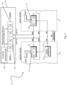
- FIG. 2 shows the communication network 14 schematically
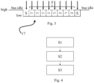
- figure 3 shows schematically a data packet exchanged in the network 14 of figure 2 using the method shown in figure 4
- the network also comprises a master device 10, a slave device 11 and a monitoring device 16 like the prior art network 14' of figure 1 , wherein the corresponding parts of the network 14 are indicated by the same references as in the prior art network 14' figure 1 but without the apostrophe.
- the description given above with respect to figure 1 is also correct for the network 14 shown in figure 2 unless stated otherwise.
- the network 14 comprises a master data processing unit 10 and a slave data processing unit 11 being connected to the master data processing unit 10 via its SPI.
- the slave data processing unit 11 is connected to the master data processing unit via a slave select line labelled by SS for indicating that data will be sent from the master data processing unit 10 to the slave data processing unit 11, a serial clock line labelled by SCK for synchronizing a sampling time of the master data processing unit 10 and a sampling time of the slave data processing unit 11, a master-out-slave-in data line labelled by MOSI for data output from the master data processing unit 10 to the slave data processing unit 11, and a master-in-slave-out data line labelled by MISO for data output from the slave data processing unit 11 to the master data processing unit 10.
- SS slave select line
- SCK serial clock line labelled by SCK
- MOSI master-out-slave-in data line labelled by MOSI
- MISO master-in-slave-out data line labelled by MISO for data output from the slave data processing unit 11 to the master data processing unit 10.
- the network 14 comprises a monitoring device/data processing unit 16 being connected to the master data processing unit 10 and to the slave data processing unit 11. Therefore, the monitoring data processing unit 16 comprises an asynchronous serial communication interface.
- the asynchronous serial communication interface of the monitoring device 16 comprises two input ports labelled by UART Rx, respectively, and two shift registers 161, 162 connected at an input side thereof to one of the input ports of the monitoring device 16, respectively.
- One of the input ports labelled by UART Rx is connected to the master-out-slave-in data line labelled by MOSI and the other one of the input ports labelled UART Rx is connected to the master-in-slave-out data line labelled by MISO.
- MISO master-in-slave-out data line
- the asynchronous serial communication interface of the monitoring device 16 also comprises a clock generator 163 (similar to the clock generator 13 of the master device 10) connected to a respective clock input of both shift registers 161, 162 of the monitoring device 16. Both shift registers 161, 162 of the monitoring device 16 have a data path for retrieving received data from the respective shift register 161, 162.
- the master device 10 indicates the start of a communication cycle including sending data from the master device 10 to the slave device 11 and vice versa using the slave select line labelled by SS, e.g., by pulling the slave select line labelled by SS from the idle/high state (i.e., 1) to the low state (i.e., 0).
- a second step S2 of the method the master and the slave device 10, 11 start sending a data packet 17 (optionally pre-) loaded into their respective shift register 12, 15 via the master-out-slave-in data line labelled by MOSI and the master-in-slave-out data line labelled by MISO (so-called duplex communication mode). More specifically, in the second step S2 sending the data from the master data processing unit 10 to the slave data processing unit 11 is done using the master-out-slave-in data line labelled by MOSI and sending data from the slave data processing unit 11 to the master data processing unit 10 is done using the master-in-slave-out data line labelled by MISO.
- the data packet 17 is shown in detail in figure 3 and comprises a start bit labelled by S (e.g., low/zero) and a stop bit (e.g., high/one) labelled by E framing/accommodating in-between a data byte labelled with F comprising eight data bits labelled with F1 - F8 (there might be more or less than eight data bits, but the data packet should contain a fixed/predefined number of data bits).
- the data (packet) 17 sent from the master data processing unit 10 to the slave data processing unit 11 and the data (packet) 17 sent from the slave data processing unit 11 to the master data processing unit 10 is framed by the start bit labelled by S as a first bit and the stop bit labelled with E as a last bit of the sent data (packet) 17.
- the master device 10 and the slave device 11 send the bits of the data packet 17 one by one starting with the start bit labelled by S, followed by the data bits labelled by F1- F8, and at the end the stop bit labelled with E.
- the bus device 10 configures its clock generator 13, using a frequency supported by the slave device 11, typically up to a few MHz, and by the monitoring device 16. Here, a predefined frequency may be used.
- the master device 10 selects the slave device 11 with a logic level 0 on the select line labelled by SS. If a waiting period is required, such as for an analog-to-digital conversion, the master device 10 waits for at least that period of time before issuing clock cycles using its clock generator 13 and the serial clock line labelled by SCK.
- the master device 10 sends a bit on the master-out-slave-in data line labelled by MOSI and the slave device 11 reads it, while the slave device 11 sends a bit on the master-in-slave-out data line labelled by MISO and the master device 10 reads it. This sequence may be maintained even when only one-directional data transfer is intended.
- the data transmission between the master and the slave device 10, 11 involves the two shift registers 12, 15 of the master and the slave device 10, 11 both having some given word-size, such as ten bits, one in the master and one in the slave device 10, 11; which are connected in a virtual ring topology by the master-out-slave-in data line labelled by MOSI and the master-in-slave-out data line labelled by MISO. Data is shifted out with the most significant bit first, here the start bit labelled with S. On the clock edge, both, the master and slave device 10, 11, shift out a bit and output it on the respective data (transmission) line (i.e., MISO and MOSI) to the counterpart.
- some given word-size such as ten bits
- each receiver 10, 11 On the next clock edge, at each receiver 10, 11 the bit is sampled from the transmission line and set as a new least-significant bit of the respective shift register 12, 15. After all the register bits have been shifted out and in, the master and slave device 10, 11 have exchanged register values. If more data needs to be exchanged, the shift registers 12, 15 are reloaded and the process repeats. Transmission may continue for any number of clock cycles.
- the master device 10 stops toggling the clock signal, and typically deselects the slave device 11 using the slave select line labelled by SS.
- the master device 10 In addition to setting the clock frequency, the master device 10 also configures a clock polarity and phase with respect to the data.
- SPI there are generally two options available, i.e., CPOL and CPHA (for clock polarity and clock phase).
- the timing is further described below and applies to both the master and the slave device 10, 11.
- CPOL determines the polarity of the clock.
- the polarities can be converted with an inverter.
- CPHA determines the timing (i.e., phase) of the data bits relative to the clock pulses.
- the "out" side holds the data valid until the leading edge of the following clock cycle.
- the slave holds the MISO line valid until slave select is deactivated.
- An alternative way of considering it is to say that a CPHA 1 cycle consists of a half cycle with the clock asserted, followed by a half cycle with the clock idle.
- the MOSI and MISO signals are usually stable (at their reception points) for the half cycle until the next clock transition.
- SPI master and slave devices 10, 11 may well sample data at different points in that half cycle. This adds more flexibility to the communication channel between the master and slave device 10, 11.
- the above ensures that the master and the slave device 10, 11 sample the received data signal at the correct point in time, i.e., they use a synchronized sampling time (indicated by the arrows shown in figure 3 ).
- the monitoring device 16 which may be considered as a man-in-the-middle device, also receives the bits labelled by S, F1-F8, and E send via the master-in-slave-out data line labelled by MISO and the master-out-slave-in data line labelled by MOSI at its respective input port labelled by UART Rx. Since the monitoring device 16 comprises the UART interface (asynchronous communication interface), the monitoring device 16 is not connected to the serial clock line labelled by SCK and thus does not receive the clock signal from the master device 10. Moreover, the monitoring device 16 does also not receive the slave/chip select signal from the master device 10 because it is not connected to the slave select line labelled by SS.
- UART interface asynchronous communication interface
- each data packet send from the master to the slave device 10, 11 and vice versa comprises the start bit labelled by S
- the monitoring device 16 can recognize a start of the above-described transmission cycle without getting the chip select signal.
- the monitoring device 16 recognizes the beginning of the data sent from the master data processing unit 10 to the slave data processing unit 11 via the master-out-slave-in data line labelled by MOSI using the start bit labelled by S and the end of the data sent from the master data processing unit 10 to the slave data processing unit 11 via the master-out-slave-in data line labelled by MOSI using the stop bit labeled by E.
Landscapes
- Engineering & Computer Science (AREA)
- Theoretical Computer Science (AREA)
- Physics & Mathematics (AREA)
- General Engineering & Computer Science (AREA)
- General Physics & Mathematics (AREA)
- Computer Networks & Wireless Communication (AREA)
- Signal Processing (AREA)
- Environmental & Geological Engineering (AREA)
- Small-Scale Networks (AREA)
- Dc Digital Transmission (AREA)
- Synchronisation In Digital Transmission Systems (AREA)
- Communication Control (AREA)
- Information Transfer Systems (AREA)
Claims (3)
- Kommunikationsverfahren für ein Kommunikationsnetzwerk (14) eines Fahrzeugs, wobei das Netzwerk umfasst:eine Master-Datenverarbeitungseinheit (10),eine Slave-Datenverarbeitungseinheit (11), die über eine synchrone serielle Kommunikationsschnittstelle mit der Master-Datenverarbeitungseinheit (10) verbunden ist, undeine Überwachungsdatenverarbeitungseinheit (16), die eine asynchrone serielle Kommunikationsschnittstelle umfasst,wobei die Slave-Datenverarbeitungseinheit (11) über eine Slave-Auswahlleitung (SS) mit der Master-Datenverarbeitungseinheit (10) zum Anzeigen, dass Daten (17) von der Master-Datenverarbeitungseinheit (10) an die Slave-Datenverarbeitungseinheit (11) und/oder von der Slave-Datenverarbeitungseinheit (11) an die Master-Datenverarbeitungseinheit (10) gesendet werden, über eine serielle Taktleitung (SCK) zur Synchronisation einer Abtastzeit der Master-Datenverarbeitungseinheit (10) und einer Abtastzeit der Slave-Datenverarbeitungseinheit (11), über eine Master-Out-Slave-In-Datenleitung (MOSI) zur Datenausgabe von der Master-Datenverarbeitungseinheit an die Slave-Datenverarbeitungseinheit und über eine Master-in-Slave-Out-Datenleitung (MISO) zur Datenausgabe von der Slave-Datenverarbeitungseinheit an die Master-Datenverarbeitungseinheit verbunden ist, undwobei die von der Master-Datenverarbeitungseinheit (10) an die Slave-Datenverarbeitungseinheit (11) und/oder von der Slave-Datenverarbeitungseinheit (11) an die Master-Datenverarbeitungseinheit (10) gesendeten Daten (17) von einem Startbit (S) als einem ersten Bit und einem Stoppbit (E) als einem letzten Bit der gesendeten Daten (17) eingerahmt werden,wobei das Verfahren umfasst:Anzeigen, dass die Daten (17) von der Master-Datenverarbeitungseinheit (10) an die Slave-Datenverarbeitungseinheit (11) und/oder von der Slave-Datenverarbeitungseinheit (11) an die Master-Datenverarbeitungseinheit (10) unter Verwendung der Slave-Auswahlleitung (SS) gesendet werden,Synchronisieren der Abtastzeit der Master-Datenverarbeitungseinheit (10) mit der Abtastzeit der Slave-Datenverarbeitungseinheit (11) unter Verwendung der seriellen Taktleitung (SCK) nach und/oder während des Anzeigens, dass die Daten (17) gesendet werden, undSenden der Daten (17) von der Master-Datenverarbeitungseinheit (10) an die Slave-Datenverarbeitungseinheit (11) unter Verwendung der Master-Out-Slave-In-Datenleitung (MO-SI) und/oder von der Slave-Datenverarbeitungseinheit (11) an die Master-Datenverarbeitungseinheit (10) unter Verwendung der Master-In-Slave-Out-Datenleitung (MI-SO), nach und/oder während des Synchronisierens der Abtastzeit der Master-Datenverarbeitungseinheit (10) mit der Abtastzeit der Slave-Datenverarbeitungseinheit (11),wobeidie Überwachungsdatenverarbeitungseinheit (16) über die asynchrone serielle Kommunikationsschnittstelle mit der Master-Out-Slave-In-Datenleitung (MOSI) und mit der Master-In-Slave-Out-Datenleitung (MISO) verbunden ist,die Überwachungsdatenverarbeitungseinheit (16) den Beginn der von der Master-Datenverarbeitungseinheit (10) an die Slave-Datenverarbeitungseinheit (11) über die Master-Out-Slave-In-Datenleitung (MOSI) gesendeten Daten (17) anhand des Startbits (S) und das Ende der von der Master-Datenverarbeitungseinheit (10) an die Slave-Datenverarbeitungseinheit (11) über die Master-Out-Slave-In-Datenleitung (MOSI) gesendeten Daten (17) unter Verwendung des Stoppbits (E) und/oder den Beginn der Daten (17), die von der Slave-Datenverarbeitungseinheit (11) an die Master-Datenverarbeitungseinheit (10) über die Master-In-Slave-Out-Datenleitung (MISO) gesendet werden, unter Verwendung des Startbits (S) und das Ende der Daten (17), die von der Slave-Datenverarbeitungseinheit (11) an die Master-Datenverarbeitungseinheit (10) über die Master-In-Slave-Out-Datenleitung (MISO) gesendet werden, unter Verwendung des Stoppbits (E) erkennt.
- Kommunikationsnetzwerk (14) für ein Fahrzeug, wobei das Netzwerk umfasst:eine Master-Datenverarbeitungseinheit (10),eine Slave-Datenverarbeitungseinheit (11), die über eine synchrone serielle Kommunikationsschnittstelle mit der Master-Datenverarbeitungseinheit (10) verbunden ist, undeine Überwachungsdatenverarbeitungseinheit (16), die eine asynchrone serielle Kommunikationsschnittstelle umfasst,wobei die Slave-Datenverarbeitungseinheit (11) über eine Slave-Auswahlleitung (SS) mit der Master-Datenverarbeitungseinheit (10) zum Anzeigen, dass Daten (17) von der Master-Datenverarbeitungseinheit (10) an die Slave-Datenverarbeitungseinheit (11) und/oder von der Slave-Datenverarbeitungseinheit (11) an die Master-Datenverarbeitungseinheit (10) gesendet werden, eine serielle Taktleitung (SCK) zum Synchronisieren einer Abtastzeit der Master-Datenverarbeitungseinheit (10) und einer Abtastzeit der Slave-Datenverarbeitungseinheit (11), eine Master-Out-Slave-In-Datenleitung (MOSI) für Daten (17), die von der Master-Datenverarbeitungseinheit an die Slave-Datenverarbeitungseinheit (11) und über eine Master-in-Slave-Out-Datenleitung (MISO) zur Datenausgabe von der Slave-Datenverarbeitungseinheit an die Master-Datenverarbeitungseinheit verbunden ist,wobei die Master-Datenverarbeitungseinheit (10) eingerichtet ist, die von der Master-Datenverarbeitungseinheit (10) an die Slave-Datenverarbeitungseinheit (11) gesendeten Daten (17) mit einem Startbit (S) als einem ersten Bit und einem Stoppbit (E) als einem letzten Bit der gesendeten Daten (17) einzurahmen, und/oder wobei die Slave-Datenverarbeitungseinheit (11) eingerichtet ist, die von der Slave-Datenverarbeitungseinheit (11) an die Master-Datenverarbeitungseinheit (10) gesendeten Daten (17) mit einem Startbit (S) als einem ersten Bit und einem Stoppbit (E) als einem letzten Bit der gesendeten Daten (17) einzurahmen,wobei die Master-Datenverarbeitungseinheit (10) eingerichtet ist anzuzeigen, dass die Daten (17) von der Master-Datenverarbeitungseinheit (10) an die Slave-Datenverarbeitungseinheit (11) und/oder von der Slave-Datenverarbeitungseinheit (11) an die Master-Datenverarbeitungseinheit (10) unter Verwendung der Slave-Auswahlleitung (SS) gesendet werden,wobei die Master-Datenverarbeitungseinheit (10) eingerichtet ist, um die Abtastzeit der Master-Datenverarbeitungseinheit (10) mit der Abtastzeit der Slave-Datenverarbeitungseinheit (11) unter Verwendung der seriellen Taktleitung (SCK) zu synchronisieren, nachdem und/oder während des Anzeigens, dass die Daten (17) gesendet werden,wobei die Master-Datenverarbeitungseinheit (10) eingerichtet ist, die Daten (17) von der Master-Datenverarbeitungseinheit (10) an die Slave-Datenverarbeitungseinheit (11) unter Verwendung der Master-Out-Slave-In-Datenleitung (MOSI) nach und/oder während der Synchronisation der Abtastzeit der Master-Datenverarbeitungseinheit (10) mit der Abtastzeit der Slave-Datenverarbeitungseinheit (11) zu senden, undwobei die Slave-Datenverarbeitungseinheit (10) eingerichtet ist, die Daten (17) von der Slave-Datenverarbeitungseinheit (10) an die Master-Datenverarbeitungseinheit (11) unter Verwendung der Master-In-Slave-Out-Datenleitung (MISO) nach und/oder während der Synchronisation der Abtastzeit der Master-Datenverarbeitungseinheit (10) mit der Abtastzeit der Slave-Datenverarbeitungseinheit (11) zu senden,wobeidie Überwachungsdatenverarbeitungseinheit (16) über die asynchrone serielle Kommunikationsschnittstelle mit der Master-Out-Slave-In-Datenleitung (MOSI) und mit der Master-In-Slave-Out-Datenleitung (MISO) verbunden ist,die Überwachungsdatenverarbeitungseinheit (16) eingerichtet ist, den Beginn der von der Master-Datenverarbeitungseinheit (10) an die Slave-Datenverarbeitungseinheit (11) über die Master-Out-Slave-In-Datenleitung (MOSI) gesendeten Daten (17) unter Verwendung des Startbits (S) und das Ende der von der Master-Datenverarbeitungseinheit (10) an die Slave-Datenverarbeitungseinheit (11) über die Master-Out-Slave-In-Datenleitung (MOSI) gesendeten Daten unter Verwendung des Stoppbits (E) zu erkennen und den Beginn der von der Slave-Datenverarbeitungseinheit (11) an die Master-Datenverarbeitungseinheit (10) über die Master-in-Slave-Out-Datenleitung (MISO) gesendeten Daten (17) unter Verwendung des Startbits (S) und das Ende der Daten, die von der Slave-Datenverarbeitungseinheit (11) an die Master-Datenverarbeitungseinheit (10) über die Master-In-Slave-Out-Datenleitung (MISO) gesendet werden, unter Verwendung des Stoppbits (E) zu erkennen.
- Fahrzeug, dadurch gekennzeichnet, dass das Fahrzeug das Netzwerk (14) nach Anspruch 2 umfasst.
Priority Applications (6)
| Application Number | Priority Date | Filing Date | Title |
|---|---|---|---|
| EP22151442.5A EP4213031B1 (de) | 2022-01-13 | 2022-01-13 | Verfahren und vorrichtung zur überwachung einer synchronen seriellen master/slave-verbindung unter verwendung einer asynchronen schnittstelle |
| CN202280088674.4A CN118541679A (zh) | 2022-01-13 | 2022-11-23 | 用于车辆的通信网络的通信方法和通信网络 |
| JP2024538117A JP2025503494A (ja) | 2022-01-13 | 2022-11-23 | 車両の通信ネットワーク用の通信方法及び通信ネットワーク |
| PCT/EP2022/082938 WO2023134911A1 (en) | 2022-01-13 | 2022-11-23 | Communication method for a communication network of a vehicle and communication network |
| US18/725,691 US20250173303A1 (en) | 2022-01-13 | 2022-11-23 | Communication Method for a Communication Network of a Vehicle and Communication Network |
| KR1020247026081A KR20240124420A (ko) | 2022-01-13 | 2022-11-23 | 차량의 통신 네트워크를 위한 통신 방법 및 통신 네트워크 |
Applications Claiming Priority (1)
| Application Number | Priority Date | Filing Date | Title |
|---|---|---|---|
| EP22151442.5A EP4213031B1 (de) | 2022-01-13 | 2022-01-13 | Verfahren und vorrichtung zur überwachung einer synchronen seriellen master/slave-verbindung unter verwendung einer asynchronen schnittstelle |
Publications (2)
| Publication Number | Publication Date |
|---|---|
| EP4213031A1 EP4213031A1 (de) | 2023-07-19 |
| EP4213031B1 true EP4213031B1 (de) | 2025-02-26 |
Family
ID=79601638
Family Applications (1)
| Application Number | Title | Priority Date | Filing Date |
|---|---|---|---|
| EP22151442.5A Active EP4213031B1 (de) | 2022-01-13 | 2022-01-13 | Verfahren und vorrichtung zur überwachung einer synchronen seriellen master/slave-verbindung unter verwendung einer asynchronen schnittstelle |
Country Status (6)
| Country | Link |
|---|---|
| US (1) | US20250173303A1 (de) |
| EP (1) | EP4213031B1 (de) |
| JP (1) | JP2025503494A (de) |
| KR (1) | KR20240124420A (de) |
| CN (1) | CN118541679A (de) |
| WO (1) | WO2023134911A1 (de) |
Family Cites Families (9)
| Publication number | Priority date | Publication date | Assignee | Title |
|---|---|---|---|---|
| US4816996A (en) | 1987-07-24 | 1989-03-28 | Motorola, Inc. | Queued serial peripheral interface for use in a data processing system |
| CN101140558A (zh) * | 2006-09-05 | 2008-03-12 | 深圳迈瑞生物医疗电子股份有限公司 | 嵌入式系统及其通信方法 |
| EP2570931A1 (de) * | 2011-09-14 | 2013-03-20 | VEGA Grieshaber KG | Verfahren zur asynchron-seriellen Datenübertragung mittels einer synchron-seriellen Schnittstelle |
| DE102013210064A1 (de) * | 2013-05-29 | 2014-12-04 | Robert Bosch Gmbh | Verfahren zur Bereitstellung einer generischen Schnittstelle sowie Mikrocontroller mit generischer Schnittstelle |
| CN108475241B (zh) * | 2016-09-29 | 2021-01-05 | 华为技术有限公司 | 一种基于spi的数据传输方法及装置 |
| US10320528B2 (en) * | 2017-04-21 | 2019-06-11 | Silicon Laboratories Inc. | Fault tolerant communication channel |
| GB2587001B (en) * | 2019-09-11 | 2023-07-19 | Idex Biometrics Asa | Two-wire host interface |
| US11210260B1 (en) * | 2020-07-29 | 2021-12-28 | Astec International Limited | Systems and methods for monitoring serial communication between devices |
| JP2024072370A (ja) * | 2022-11-16 | 2024-05-28 | ローム株式会社 | 半導体装置、および通信システム |
-
2022
- 2022-01-13 EP EP22151442.5A patent/EP4213031B1/de active Active
- 2022-11-23 JP JP2024538117A patent/JP2025503494A/ja active Pending
- 2022-11-23 WO PCT/EP2022/082938 patent/WO2023134911A1/en not_active Ceased
- 2022-11-23 US US18/725,691 patent/US20250173303A1/en active Pending
- 2022-11-23 CN CN202280088674.4A patent/CN118541679A/zh active Pending
- 2022-11-23 KR KR1020247026081A patent/KR20240124420A/ko active Pending
Also Published As
| Publication number | Publication date |
|---|---|
| EP4213031A1 (de) | 2023-07-19 |
| JP2025503494A (ja) | 2025-02-04 |
| WO2023134911A1 (en) | 2023-07-20 |
| CN118541679A (zh) | 2024-08-23 |
| KR20240124420A (ko) | 2024-08-16 |
| US20250173303A1 (en) | 2025-05-29 |
Similar Documents
| Publication | Publication Date | Title |
|---|---|---|
| US8195857B2 (en) | Coupling devices, system comprising a coupling device and method for use in a system comprising a coupling device | |
| CN103210384B (zh) | 用于在处理器模块之间传输数据的方法和电路装置 | |
| EP2221731B1 (de) | Bidirektionale Verbindungsschnittstelle mit geringer Leistung, geringer Pinzahl und doppelter Datenrate | |
| US9336167B2 (en) | I2C controller register, control, command and R/W buffer queue logic | |
| EP0258872B1 (de) | Serielles Datenübertragungssystem | |
| US20050254518A1 (en) | Communication message conversion device, communication method and communication system | |
| US20040205267A1 (en) | Bridge for removing master-induced stalls on a data bus | |
| CN105677598B (zh) | 基于i2c接口快速读取多个mems传感器数据的模块和方法 | |
| EP4323880B1 (de) | I2c-busarchitektur mit gemeinsamem takt und zugeordneten datenleitungen | |
| KR19990022324A (ko) | 주변 소자 상호연결 버스상의 버스트 전송 시스템및 방법 | |
| EP2725500A1 (de) | Serielle Kommunikationsschaltung, integrierte Schaltvorrichtung, Vorrichtung zur Messung physikalischer Größen, elektronische Vorrichtung, ein sich bewegendes Objekt und serielles Kommunikationsverfahren | |
| CN102088386A (zh) | 一种电路系统主从互联模块的串行总线 | |
| US20090271557A1 (en) | Non-volatile memory storage device with high transmission rate | |
| KR20210075878A (ko) | I2c와의 하위 호환성을 촉진하는 i3c 허브 | |
| US10050764B2 (en) | Method for communicating data, communication controller and circuit arrangement | |
| US8458389B2 (en) | Apparatus and method for converting protocol interface | |
| EP4213031A1 (de) | Verfahren und vorrichtung zur überwachung einer synchronen seriellen master/slave-verbindung unter verwendung einer asynchronen schnittstelle | |
| TWI727581B (zh) | 資料傳輸系統 | |
| JPH11502643A (ja) | シリアルデータバスシステムにおけるエラーの認識及び除去 | |
| EP0637156A1 (de) | Speicherschnittstellesystem | |
| Wu et al. | The research and implementation of interfacing based on PCI express | |
| EP4332784B1 (de) | Halbleiterbauelement und kommunikationsverfahren in dem halbleiterbauelement | |
| CN217880048U (zh) | 车载摄像头数据分析系统 | |
| CN118511485A (zh) | 车载电气系统的控制装置 | |
| CN119728338A (zh) | 一种基于SocketCAN通信协议的ADAS部署方法 |
Legal Events
| Date | Code | Title | Description |
|---|---|---|---|
| PUAI | Public reference made under article 153(3) epc to a published international application that has entered the european phase |
Free format text: ORIGINAL CODE: 0009012 |
|
| STAA | Information on the status of an ep patent application or granted ep patent |
Free format text: STATUS: THE APPLICATION HAS BEEN PUBLISHED |
|
| AK | Designated contracting states |
Kind code of ref document: A1 Designated state(s): AL AT BE BG CH CY CZ DE DK EE ES FI FR GB GR HR HU IE IS IT LI LT LU LV MC MK MT NL NO PL PT RO RS SE SI SK SM TR |
|
| STAA | Information on the status of an ep patent application or granted ep patent |
Free format text: STATUS: REQUEST FOR EXAMINATION WAS MADE |
|
| 17P | Request for examination filed |
Effective date: 20240119 |
|
| RBV | Designated contracting states (corrected) |
Designated state(s): AL AT BE BG CH CY CZ DE DK EE ES FI FR GB GR HR HU IE IS IT LI LT LU LV MC MK MT NL NO PL PT RO RS SE SI SK SM TR |
|
| GRAP | Despatch of communication of intention to grant a patent |
Free format text: ORIGINAL CODE: EPIDOSNIGR1 |
|
| STAA | Information on the status of an ep patent application or granted ep patent |
Free format text: STATUS: GRANT OF PATENT IS INTENDED |
|
| RIC1 | Information provided on ipc code assigned before grant |
Ipc: H04L 43/0823 20220101ALI20240806BHEP Ipc: H04L 43/024 20220101ALI20240806BHEP Ipc: G06F 13/42 20060101AFI20240806BHEP |
|
| INTG | Intention to grant announced |
Effective date: 20240910 |
|
| GRAS | Grant fee paid |
Free format text: ORIGINAL CODE: EPIDOSNIGR3 |
|
| GRAA | (expected) grant |
Free format text: ORIGINAL CODE: 0009210 |
|
| STAA | Information on the status of an ep patent application or granted ep patent |
Free format text: STATUS: THE PATENT HAS BEEN GRANTED |
|
| AK | Designated contracting states |
Kind code of ref document: B1 Designated state(s): AL AT BE BG CH CY CZ DE DK EE ES FI FR GB GR HR HU IE IS IT LI LT LU LV MC MK MT NL NO PL PT RO RS SE SI SK SM TR |
|
| REG | Reference to a national code |
Ref country code: GB Ref legal event code: FG4D |
|
| REG | Reference to a national code |
Ref country code: CH Ref legal event code: EP |
|
| REG | Reference to a national code |
Ref country code: DE Ref legal event code: R096 Ref document number: 602022010960 Country of ref document: DE |
|
| REG | Reference to a national code |
Ref country code: IE Ref legal event code: FG4D |
|
| REG | Reference to a national code |
Ref country code: NL Ref legal event code: MP Effective date: 20250226 |
|
| PG25 | Lapsed in a contracting state [announced via postgrant information from national office to epo] |
Ref country code: RS Free format text: LAPSE BECAUSE OF FAILURE TO SUBMIT A TRANSLATION OF THE DESCRIPTION OR TO PAY THE FEE WITHIN THE PRESCRIBED TIME-LIMIT Effective date: 20250526 |
|
| PG25 | Lapsed in a contracting state [announced via postgrant information from national office to epo] |
Ref country code: FI Free format text: LAPSE BECAUSE OF FAILURE TO SUBMIT A TRANSLATION OF THE DESCRIPTION OR TO PAY THE FEE WITHIN THE PRESCRIBED TIME-LIMIT Effective date: 20250226 |
|
| PG25 | Lapsed in a contracting state [announced via postgrant information from national office to epo] |
Ref country code: PL Free format text: LAPSE BECAUSE OF FAILURE TO SUBMIT A TRANSLATION OF THE DESCRIPTION OR TO PAY THE FEE WITHIN THE PRESCRIBED TIME-LIMIT Effective date: 20250226 |
|
| PG25 | Lapsed in a contracting state [announced via postgrant information from national office to epo] |
Ref country code: ES Free format text: LAPSE BECAUSE OF FAILURE TO SUBMIT A TRANSLATION OF THE DESCRIPTION OR TO PAY THE FEE WITHIN THE PRESCRIBED TIME-LIMIT Effective date: 20250226 |
|
| REG | Reference to a national code |
Ref country code: LT Ref legal event code: MG9D |
|
| PG25 | Lapsed in a contracting state [announced via postgrant information from national office to epo] |
Ref country code: IS Free format text: LAPSE BECAUSE OF FAILURE TO SUBMIT A TRANSLATION OF THE DESCRIPTION OR TO PAY THE FEE WITHIN THE PRESCRIBED TIME-LIMIT Effective date: 20250626 Ref country code: NO Free format text: LAPSE BECAUSE OF FAILURE TO SUBMIT A TRANSLATION OF THE DESCRIPTION OR TO PAY THE FEE WITHIN THE PRESCRIBED TIME-LIMIT Effective date: 20250526 |
|
| PG25 | Lapsed in a contracting state [announced via postgrant information from national office to epo] |
Ref country code: NL Free format text: LAPSE BECAUSE OF FAILURE TO SUBMIT A TRANSLATION OF THE DESCRIPTION OR TO PAY THE FEE WITHIN THE PRESCRIBED TIME-LIMIT Effective date: 20250226 |
|
| PG25 | Lapsed in a contracting state [announced via postgrant information from national office to epo] |
Ref country code: HR Free format text: LAPSE BECAUSE OF FAILURE TO SUBMIT A TRANSLATION OF THE DESCRIPTION OR TO PAY THE FEE WITHIN THE PRESCRIBED TIME-LIMIT Effective date: 20250226 |
|
| PG25 | Lapsed in a contracting state [announced via postgrant information from national office to epo] |
Ref country code: PT Free format text: LAPSE BECAUSE OF FAILURE TO SUBMIT A TRANSLATION OF THE DESCRIPTION OR TO PAY THE FEE WITHIN THE PRESCRIBED TIME-LIMIT Effective date: 20250626 Ref country code: LV Free format text: LAPSE BECAUSE OF FAILURE TO SUBMIT A TRANSLATION OF THE DESCRIPTION OR TO PAY THE FEE WITHIN THE PRESCRIBED TIME-LIMIT Effective date: 20250226 |
|
| PG25 | Lapsed in a contracting state [announced via postgrant information from national office to epo] |
Ref country code: GR Free format text: LAPSE BECAUSE OF FAILURE TO SUBMIT A TRANSLATION OF THE DESCRIPTION OR TO PAY THE FEE WITHIN THE PRESCRIBED TIME-LIMIT Effective date: 20250527 Ref country code: BG Free format text: LAPSE BECAUSE OF FAILURE TO SUBMIT A TRANSLATION OF THE DESCRIPTION OR TO PAY THE FEE WITHIN THE PRESCRIBED TIME-LIMIT Effective date: 20250226 |
|
| REG | Reference to a national code |
Ref country code: AT Ref legal event code: MK05 Ref document number: 1771336 Country of ref document: AT Kind code of ref document: T Effective date: 20250226 |
|
| PG25 | Lapsed in a contracting state [announced via postgrant information from national office to epo] |
Ref country code: SE Free format text: LAPSE BECAUSE OF FAILURE TO SUBMIT A TRANSLATION OF THE DESCRIPTION OR TO PAY THE FEE WITHIN THE PRESCRIBED TIME-LIMIT Effective date: 20250226 |
|
| PG25 | Lapsed in a contracting state [announced via postgrant information from national office to epo] |
Ref country code: SM Free format text: LAPSE BECAUSE OF FAILURE TO SUBMIT A TRANSLATION OF THE DESCRIPTION OR TO PAY THE FEE WITHIN THE PRESCRIBED TIME-LIMIT Effective date: 20250226 |
|
| PG25 | Lapsed in a contracting state [announced via postgrant information from national office to epo] |
Ref country code: DK Free format text: LAPSE BECAUSE OF FAILURE TO SUBMIT A TRANSLATION OF THE DESCRIPTION OR TO PAY THE FEE WITHIN THE PRESCRIBED TIME-LIMIT Effective date: 20250226 |
|
| PG25 | Lapsed in a contracting state [announced via postgrant information from national office to epo] |
Ref country code: AT Free format text: LAPSE BECAUSE OF FAILURE TO SUBMIT A TRANSLATION OF THE DESCRIPTION OR TO PAY THE FEE WITHIN THE PRESCRIBED TIME-LIMIT Effective date: 20250226 |
|
| PG25 | Lapsed in a contracting state [announced via postgrant information from national office to epo] |
Ref country code: EE Free format text: LAPSE BECAUSE OF FAILURE TO SUBMIT A TRANSLATION OF THE DESCRIPTION OR TO PAY THE FEE WITHIN THE PRESCRIBED TIME-LIMIT Effective date: 20250226 Ref country code: CZ Free format text: LAPSE BECAUSE OF FAILURE TO SUBMIT A TRANSLATION OF THE DESCRIPTION OR TO PAY THE FEE WITHIN THE PRESCRIBED TIME-LIMIT Effective date: 20250226 |
|
| PG25 | Lapsed in a contracting state [announced via postgrant information from national office to epo] |
Ref country code: RO Free format text: LAPSE BECAUSE OF FAILURE TO SUBMIT A TRANSLATION OF THE DESCRIPTION OR TO PAY THE FEE WITHIN THE PRESCRIBED TIME-LIMIT Effective date: 20250226 |
|
| PG25 | Lapsed in a contracting state [announced via postgrant information from national office to epo] |
Ref country code: SK Free format text: LAPSE BECAUSE OF FAILURE TO SUBMIT A TRANSLATION OF THE DESCRIPTION OR TO PAY THE FEE WITHIN THE PRESCRIBED TIME-LIMIT Effective date: 20250226 |
|
| REG | Reference to a national code |
Ref country code: DE Ref legal event code: R097 Ref document number: 602022010960 Country of ref document: DE |
|
| PLBE | No opposition filed within time limit |
Free format text: ORIGINAL CODE: 0009261 |
|
| STAA | Information on the status of an ep patent application or granted ep patent |
Free format text: STATUS: NO OPPOSITION FILED WITHIN TIME LIMIT |
|
| 26N | No opposition filed |
Effective date: 20251127 |
|
| PGFP | Annual fee paid to national office [announced via postgrant information from national office to epo] |
Ref country code: GB Payment date: 20260122 Year of fee payment: 5 |
|
| PGFP | Annual fee paid to national office [announced via postgrant information from national office to epo] |
Ref country code: DE Payment date: 20260121 Year of fee payment: 5 |
|
| PGFP | Annual fee paid to national office [announced via postgrant information from national office to epo] |
Ref country code: IT Payment date: 20260130 Year of fee payment: 5 |
|
| PGFP | Annual fee paid to national office [announced via postgrant information from national office to epo] |
Ref country code: FR Payment date: 20260128 Year of fee payment: 5 |